Fairchild Semiconductor H11B815 Datasheet

4-PIN PHOTODARLINGTON
OPTOCOUPLER
H11B815
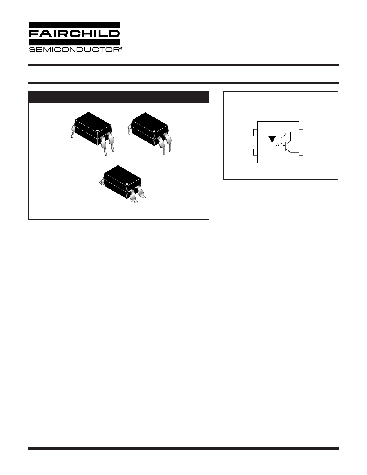
PACKAGE
4
1
4
4
CATHODE
1
1
SCHEMATIC
1
2
4
COLLECTORANODE
3EMITTER
DESCRIPTION
The H11B815 consists of a gallium arsenide infrared emitting diode driving a silicon Darlington phototransistor in a 4-pin dual
in-line package.
FEATURES
• Compact 4-pin package
• Current Transfer Ratio: 600% minimum (at I
• High isolation voltage between input and output (5300 VRMS)
• UL recognized (File # E90700)
= 1 mA)
F
APPLICATIONS
•Power Supply Monitors
• Relay Contact Monitor
•Telephone/Telegraph Line Receiver
•Twisted Pair Line Receiver
• Digital Logic/Digital Logic
© 2002 Fairchild Semiconductor Corporation
Page 1 of 9
3/26/03

4-PIN PHOTODARLINGTON
OPTOCOUPLER
H11B815
ABSOLUTE MAXIMUM RATINGS
(No derating required up to 85°C)
Parameter Symbol Value Units
TOTAL DEVICE
Storage Temperature
Operating Temperature
Lead Solder Temperature
Total Device Power Dissipation @ T
= 25°C P
A
T
T
T
STG
OPR
SOL
D
-55 to +150 °C
-55 to +100 °C
260 for 10 sec °C
250 mW
EMITTER
I
V
F
P
I
F
R
(pk)
D
80 mA
6V
1A
140 mW
DC/Average Forward Input Current
Reverse Input Voltage
Forward Current - Peak (1µs pulse, 300pps)
LED Power Dissipation @ T
= 25°C
A
Derate above 25°C 1.33 mW/°C
DETECTOR
Collector-Emitter Voltage
Emitter-Collector Voltage
Continuous Collector Current
Detector Power Dissipation @ T
= 25°C
A
Derate above 25°C 2.0 mW/°C
V
V
CEO
ECO
I
C
P
D
35 V
6V
200 mA
200 mW
(T
ELECTRICAL CHARACTERISTICS
= 25°C Unless otherwise specified.)
A
INDIVIDUAL COMPONENT CHARACTERISTICS
Parameter Test Conditions Symbol Min Typ** Max Unit
EMITTER
= 20 mA) V
Input Forward Voltage
Reverse Leakage Current
DETECTOR
Collector-Emitter Breakdown Voltage
Emitter-Collector Breakdown Voltage
Collector-Emitter Dark Current
Capacitance
© 2002 Fairchild Semiconductor Corporation
(I
F
(V
= 6.0 V) I
R
(I
= 1.0 mA, I
C
(I
= 100 µA, I
E
(V
= 10 V, I
CE
(V
= 0 V, f = 1 MHz) C
CE
= 0) BV
F
= 0) BV
F
= 0) I
F
Page 2 of 9
F
R
CEO
ECO
CEO
CE
35 60 V
68 V
1.2 1.50 V
0.001 10 µA
0.005 1 µA
8pF
3/26/03

Ω
4-PIN PHOTODARLINGTON
OPTOCOUPLER
H11B815
TRANSFER CHARACTERISTICS
DC Characteristic Test Conditions Symbol Min Typ** Max Units
(I
Current Transfer Ratio, Collector-Emitter
Saturation Voltage
Rise Time (non saturated)
Fall Time (non saturated)
(I
= 10 mA, V
C
(I
= 10 mA, V
C
= 1 mA, V
F
= 20 mA, I
(I
F
= 2 V, R
CE
= 2 V, R
CE
= 2 V)
CE
= 5 mA) V
C
= 100V) t
L
= 100V) t
L
CTR 600 7,500 %
CE(sat)
r
f
0.8 1.0 V
300 µs
250 µs
ISOLATION CHARACTERISTICS
Characteristic Test Conditions Symbol Min Typ** Max Units
(I
Input-Output Isolation Voltage
Isolation Resistance
Isolation Capacitance
** All typicals at TA = 25°C
[ 1 µA, 1 min.) V
I-O
(V
= 500 VDC) R
I-O
(V
= &, f = 1 MHz) C
I-O
ISO
ISO
ISO
5300 Vac(rms)
11
10
0.5 pf
© 2002 Fairchild Semiconductor Corporation
Page 3 of 9
3/26/03
 Loading...