

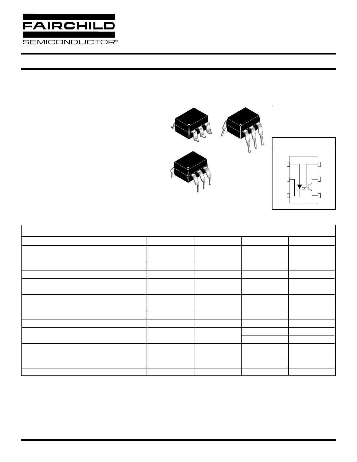
DESCRIPTION
The H11AG series consists of a Gallium-AluminumArsenide IRED emitting diode coupled with a silicon
phototransistor in a dual in-line package. This device
provides the unique feature of the high current transfer
ratio at both low output voltage and low input current.
This makes it ideal for use in low power logic circuits,
telecommunications equipment and portable electronics
isolation applications.
PHOTOTRANSISTOR OPTOCOUPLERS
H11AG1 H11AG2 H11AG3
APPLICATIONS
• CMOS driven solid state reliability
• Telephone ring detector
• Digital logic isolation
FEATURES
• High efficiency low degradation liquid epitaxial IRED
• Logic level compatible, input and output currents, with
CMOS and LS/TTL
• High DC current transfer ratio at low input currents
• Underwriters Laboratory (UL) recognized File #E90700
6
1
6
1
6
1
SCHEMATIC
Parameters Symbol Device Value Units
TOTAL DEVICE
T
STG
All -55 to +150 °C
Storage Temperature
Operating Temperature T
OPR
All -55 to +100 °C
Lead Solder Temperature T
SOL
All 260 for 10 sec °C
Total Device Power Dissipation @ 25°C (LED plus detector)
P
D
All
260 mW
Derate Linearly From 25°C 3.5 mW/°C
EMITTER
I
F
All 50 mA
Continuous Forward Current
Reverse Voltage V
R
All 6 V
Forward Current - Peak (1 µs pulse, 300 pps) IF(pk) All 3.0 A
LED Power Dissipation 25°C Ambient
P
D
All
75 mW
Derate Linearly From 25°C 1.0 mW/°C
DETECTOR
Detector Power Dissipation @ 25°C
P
D
All
150 mW
Derate Linearly from 25°C 2.0 mW/°C
Continuous Collector Current All 50 mA
2001 Fairchild Semiconductor Corporation
DS300213 1/28/02 1 OF 8 www.fairchildsemi.com
ABSOLUTE MAXIMUM RATINGS
ANODE
1
CATHODE
2
3
N/C
6
BASE
5COL
4 EMITTER
Parameters Test Conditions Symbol Device Min Typ Max Units
EMITTER
Input Forward Voltage I
F
= 1 mA
V
F
All
1.5 V
Reverse Leakage Current
V
R
= 5 V, TA= 25°C
I
R
All 10 µA
V
R
= 5 V, TA= 70°C
I
R
All 100 µA
Capacitance V = 0, f = 1.0 MHz
C
J
All 100 pF
DETECTOR
Breakdown Voltage
Collector to Emitter I
C
= 1.0 mA, IF= 0 BV
CEO
All 30
V
Collector to Base IC= 100 µA, IF= 0 BV
CBO
All 70 V
Emitter to Collector IC= 100 µA, IF= 0 BV
ECO
All 7 V
Leakage Current
Collector to Emitter V
CE
= 10 V, IF= 0 I
CEO
All 5 10
µA
Capacitance
V
CE
= 10 V, f = 1 MHz C
CE
All 2
pF
INDIVIDUAL COMPONENT CHARACTERISTICS
ELECTRICAL CHARACTERISTICS
(TA= 0-70°CUnless otherwise specified.)
DC Characteristics Test Conditions Symbol Device Min Typ Max Units
H11AG1 300
I
F
= 1 mA, VCE= 5 V CTR H11AG2 200
H11AG3 100
H11AG1 100
Current Transfer Ratio
I
F
= 1 mA, VCE= 0.6 V CTR
H11AG2 50
%
H11AG3 20
IF= 0.2 mA, VCE= 1.5 V CTR
H11AG1 100
H11AG2 50
Saturation Voltage
I
F
= 2.0 mA, IC= 0.5 mA
V
CE(SAT)
All .40 V
AC Characteristics Test Conditions Symbol Device Min Typ Max Units
Non-Saturated Switching Times
Turn-On Time R
L
= 100 Ω, IF= 1 mA, VCC= 5 V
t
on
All 5 µS
Turn-Off Time R
L
= 100 Ω, IF= 1 mA, VCC= 5 V
t
off
All 5 µS
TRANSFER CHARACTERISTICS
(TA= 25°C Unless otherwise specified.)
www.fairchildsemi.com 2 OF 8 1/28/02 DS300213
Parameters Test Conditions Symbol Min Typ Max Units
Input-Output Isolation Voltage I
I-0
≤ 1 µA, t = 1 min. V
ISO
5300 Vac(rms)
ISOLATION CHARACTERISTICS
PHOTOTRANSISTOR OPTOCOUPLERS
H11AG1 H11AG2 H11AG3
DS300213 1/28/02 3 OF 8 www.fairchildsemi.com
PHOTOTRANSISTOR OPTOCOUPLERS
H11AG1 H11AG2 H11AG3
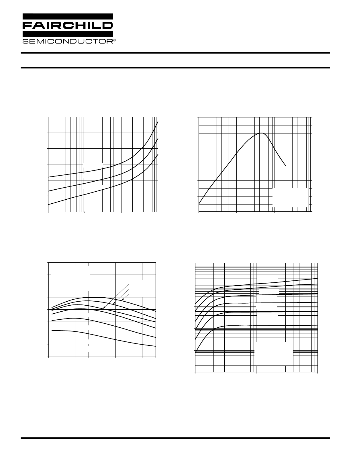
Figure 1. LED Forward Voltage vs. Forward Current
2.0
1.8
)
V
(
E
1.6
G
A
T
L
O
V
1.4
D
R
A
W
R
O
1.2
F
-
F
V
T
= -55oC
A
= 25
T
A
= 100oC
T
A
o
C
1.0
0.8
0.1 1 10 100
IF - LED FORWARD CURRENT (mA)
Figure 3. Normalized CTR vs. Temperature
1.6
NORMALIZED TO:
= 5mA
I
1.4
F
V
= 5V
CE
1.2
E
C
R
T
1.0
C
D
E
Z
I
0.8
L
A
M
R
0.6
O
N
0.4
0.2
0.0
-60 -40 -20 0 20 40 60 80 100
o
T
= 25
C
A
I
= 1mA
F
I
= 0.5mA
F
IF = 0.2mA
T
- AMBIENT TEMPERATURE -
A
o
C
= 10mA
I
F
IF = 2mA
= 5mA
I
F
Figure 2. Normalized Current Transfer Ratio vs. Forward Current
1.2
1.0
E
C
0.8
R
T
C
D
E
0.6
Z
I
L
A
M
R
O
0.4
N
NORMALIZED TO:
= 5mA
I
0.2
F
= 5V
V
CE
= 25
T
A
0.1 1 10 100
IF - FORWARD CURRENT - mA
Figure 4. Normalized Collector vs. Collector - Emitter Voltage
10
T
N
E
R
R
1
U
C
R
E
T
T
I
M
E
0.1
R
O
T
C
E
L
L
0.01
O
C
-
E
C
I
D
E
0.001
Z
I
L
A
M
R
O
N
0.0001
0.1 1 10
V
- COLLECTOR - EMITTER VOLTAGE - V
CE
I
= 10mA
F
= 5mA
I
F
I
= 2mA
F
I
= 1mA
F
IF = 0.5mA
I
= 0.2mA
F
NORMALIZED TO:
= 5mA
I
F
V
= 5V
CE
= 25oC
T
A
o
C

www.fairchildsemi.com 4 OF 8 1/28/02 DS300213
PHOTOTRANSISTOR OPTOCOUPLERS
H11AG1 H11AG2 H11AG3
Figure 5. Normalized Collector Base Photocurrent Ratio vs. Forward Current
T
N
30
E
R
R
U
C
O
25
T
O
H
P
E
20
S
A
B
R
O
T
15
C
E
L
L
O
C
10
B
C
I
D
E
5
Z
I
L
A
M
R
0
O
N
0 102030405060708090100
NORMALIZED TO:
= 5mA
I
F
V
= 5V
CB
o
T = 25
C
A
IF - FORWARD CURRENT - mA
Figure 7. Collector-Emitter Dark Current vs. Ambient Temperature
10000
Figure 6. Normalized Collector - Base Current vs. Temperature
10
T
N
E
R
R
U
1
C
E
S
A
B
R
O
T
0.1
C
E
L
L
O
C
D
E
Z
I
0.01
L
A
M
R
O
N
NORMALIZED TO:
= 5mA
I
F
= 5V
V
CB
= 25oC
T
A
0.001
-60 -40 -20 0 20 40 60 80 100
TA - AMBIENT TEMPERATURE - oC
= 10mA
I
F
IF = 5mA
IF = 2mA
IF = 1mA
I
= 0.5mA
F
IF = 0.2mA
IF = 0mA
V
= 10V
CE
1000
)
A
n
(
T
N
100
E
R
R
U
C
K
R
10
A
D
-
O
E
C
I
1
0.1
0 102030405060708090100
TA - AMBIENT TEMPERATURE (oC)

The H1 1AG1’s superior performance at low input currents allows standard CMOS logic circuits to directly operate a 25A solid state relay.
Circuit operation is as follows: power switching is provided by the SC160B, 25A triac. Its gate is controlled by the C203B via the DT230H
rectifier bridge. The C203B turn-on is inhibited by the 2N4256 when line voltage is above 12V and/or the H1 1AG is off. False trigger and
dv/dt protection are provided by the combination of the MOV varistor and RC snubber network.
The H11AG1 uses less input power than the neon bulb traditionally used to monitor telephone and line voltages. Additionally. response
time can be tailored to ignore telephone dial tap, switching transients and other undesired signals by modifying the value of C2. The high
impedance to line voltage also can simply board layout spacing requirements.
INPUT R
1
C
1
Z
40-90 VRMS 75 K 0.1 µF
109K
20 Hz 1/10 W 100 V
95-135 VRMS 180 K 12 ηF
285K
60 Hz 1/10 W 200 V
200-280 VRMS 390 K 6.80 ηF
550K
50/60 Hz 1/4 W 400 V
DC component of input voltage is ignored due to C1
DS300213 1/28/02 5 OF 8 www.fairchildsemi.com
PHOTOTRANSISTOR OPTOCOUPLERS
H11AG1 H11AG2 H11AG3
+5V
CMOS
CONTROL
15K
≥ 0.16mA
H11AG1
22K
1.5MΩ
2N4256
150pF
75KΩ 47Ω
C203D
47Ω
SC160B
DT230H
(4)
0.1
≤ 25A
LOAD
120V
60Hz
SUPPLY
V130LA20A
Figure 8. CMOS Input, 3KW, Zero Voltage Switching Solid State Relay
3V ≤ VCC ≤ 10V
47KΩ
AC
INPUT
VOLT AGE
R
C
1
1N148
1
H11AG1
4.7MΩ
C
0.1
4093 or
74HC14
4.7KΩ
2
Figure 9. Telephone Ring Detector/A.C. Line CMOS Input Isolator

Lead Coplanarity : 0.004 (0.10) MAX
0.270 (6.86)
0.240 (6.10)
0.350 (8.89)
0.330 (8.38)
0.300 (7.62)
TYP
0.405 (10.30)
MAX
0.315 (8.00)
MIN
0.016 (0.40) MIN
2
5
PIN 1
ID.
0.016 (0.41)
0.008 (0.20)
0.100 (2.54)
TYP
0.022 (0.56)
0.016 (0.41)
0.070 (1.78)
0.045 (1.14)
0.200 (5.08)
0.165 (4.18)
4
3
0.020 (0.51)
MIN
1
6
0.100 (2.54)
TYP
0.020 (0.51)
MIN
0.350 (8.89)
0.330 (8.38)
0.270 (6.86)
0.240 (6.10)
PIN 1
ID.
0.022 (0.56)
0.016 (0.41)
0.070 (1.78)
0.045 (1.14)
0.200 (5.08)
0.135 (3.43)
0.300 (7.62)
TYP
0° to 15°
0.154 (3.90)
0.100 (2.54)
SEATING PLANE
0.016 (0.40)
0.008 (0.20)
SEATING PLANE
0.016 (0.40)
0.008 (0.20)
0.070 (1.78)
0.045 (1.14)
0.350 (8.89)
0.330 (8.38)
0.154 (3.90)
0.100 (2.54)
0.200 (5.08)
0.135 (3.43)
0.004 (0.10)
MIN
0.270 (6.86)
0.240 (6.10)
0.400 (10.16)
TYP
0° to 15°
0.022 (0.56)
0.016 (0.41)
0.100 (2.54) TYP
NOTE
All dimensions are in inches (millimeters)
0.070 (1.78)
0.060 (1.52)
0.030 (0.76)
0.100 (2.54)
0.295 (7.49)
0.415 (10.54)
Package Dimensions (Surface Mount)Package Dimensions (Through Hole)
Package Dimensions (0.4”Lead Spacing) Recommended Pad Layout for
Surface Mount Leadform
www.fairchildsemi.com 6 OF 8 1/28/02 DS300213
PHOTOTRANSISTOR OPTOCOUPLERS
H11AG1 H11AG2 H11AG3

S .S Surface Mount Lead Bend
SD .SD Surface Mount; Tape and reel
W.W0.4” Lead Spacing
300 .300 VDE 0884
300W .300W VDE 0884, 0.4” Lead Spacing
3S .3S VDE 0884, Surface Mount
3SD .3SD VDE 0884, Surface Mount, Tape & Reel
Option
Order Entry Identifier
Description
4.0 ± 0.1
Ø1.55 ± 0.05
User Direction of Feed
4.0 ± 0.1
1.75 ± 0.10
7.5 ± 0.1
16.0 ± 0.3
12.0 ± 0.1
0.30 ± 0.05
13.2 ± 0.2
4.85 ± 0.20
0.1 MAX
10.30 ± 0.20
9.55 ± 0.20
Ø1.6 ± 0.1
Carrier Tape Specifications (“D” Taping Orientation)
NOTE
All dimensions are millimeters
DS300213 1/28/02 7 OF 8 www.fairchildsemi.com
PHOTOTRANSISTOR OPTOCOUPLERS
H11AG1 H11AG2 H11AG3

DISCLAIMER
FAIRCHILD SEMICONDUCTOR RESERVES THE THE RIGHT TO MAKE CHANGES WITHOUT FURTHER NOTICE
TO ANY PRODUCTS HEREIN TO IMPROVE RELIABILITY, FUNCTION OR DESIGN. FAIRCHILD DOES NOT
ASSUME ANY LIABILITY ARISING OUT OF THE APPLICATION OR USE OF ANY PRODUCT OR CIRCUIT
DESCRIBED HEREIN; NEITHER DOES IT CONVEY ANY LICENSE UNDER ITS PATENT RIGHTS, NOR THE
RIGHTS OF OTHERS.
LIFE SUPPORT POLICY
FAIRCHILD’S PRODUCTS ARE NOT AUTHORIZED FOR USE AS CRITICAL COMPONENTS IN LIFE SUPPORT
DEVICES OR SYSTEMS WITHOUT THE EXPRESS WRITTEN APPROVAL OF THE PRESIDENT OF FAIRCHILD
SEMICONDUCTOR CORPORATION. As used herein:
1. Life support devices or systems are devices or
systems which, (a) are intended for surgical
implant into the body,or (b) support or sustain life,
and (c) whose failure to perform when properly
used in accordance with instructions for use provided
in labeling, can be reasonably expected to result in a
significant injury of the user.
2. A critical component in any component of a life support
device or system whose failure to perform can be
reasonably expected to cause the failure of the life
support device or system, or to affect its safety or
effectiveness.
www.fairchildsemi.com 8 OF 8 1/28/02 DS300213
PHOTOTRANSISTOR OPTOCOUPLERS
H11AG1 H11AG2 H11AG3
 Loading...