

Fairchild Semiconductor CD4023BCSJX, CD4023BCSJ, CD4023BCN, CD4023BCMX, CD4023BCM Datasheet
© 2000 Fairchild Semiconductor Corporation DS005956 www.fairchildsemi.com
October 1987
Revised August 2000
CD4023BC Buffered Triple 3-Input NAND Gate
CD4023BC
Buffered Triple 3-Input NAND Gate
General Description
These triple gates are monolithic complementary MOS
(CMOS) integrated circuits constructed with N- and Pchannel enhancement mode transistors. They have eq ual
source and sink current capabilities and confo rm to standard B series output drive. The devices also ha ve buffered
outputs which improve tra nsfe r ch ar acte risti cs b y pr ovid ing
very high gain. All inputs are protected against static discharge with diodes to V
DD
and VSS.
Features
■ Wide supply voltage range: 3.0V to 15V
■ High noise immunity: 0.45 V
DD
(typ)
■ Low power TTL compatibility:
fan out of 2 driving 74L or 1 driving 74LS
■ 5V–10V–15V parametric ratings
■ Symmetrical output characteristics
■ Maximum input leakage 1
µA at 15V over full
temperature range
Ordering Code:
Devices also availab le in Tape and Reel. Specify by appending th e s uffix let t er “X” tot he ordering code.
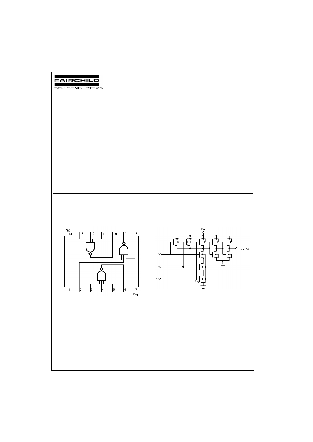
Connection Diagram
Top View
Block Diagram
1
/3 Device Shown
*All Inputs Protected by Standard CMOS Input Protection Circuit.
Order Number Package Number Package Description
CD4023BCM M14A 14-Lead Small Outline Integrated Circuit (SOIC), JEDEC MS-120, 0.150 Narrow
CD4023BCS M14D 14-Lead Small Outline Package (SOP), EIAJ TYPE II, 5.3mm Wide
CD4023BCN N14A 14-Lead Plastic Dual-In-Line Package (PDIP), JEDEC MS-001, 0.300 Wide
www.fairchildsemi.com 2
CD4023BC
Absolute Maximum Ratings(Note 1)
(Note 2)
Recommended Operating
Conditions
Note 1: “Absolute Maximum Ratings” are those values beyond which the
safety of the device cannot be guaranteed; they are not meant to imply that
the devices should be operated at these limits. The table of “Recom-
mended Operating Conditions” and “Electrical Characteristics” provides
conditions for actua l device operation.
Note 2: V
SS
= 0V unless otherwise specified.
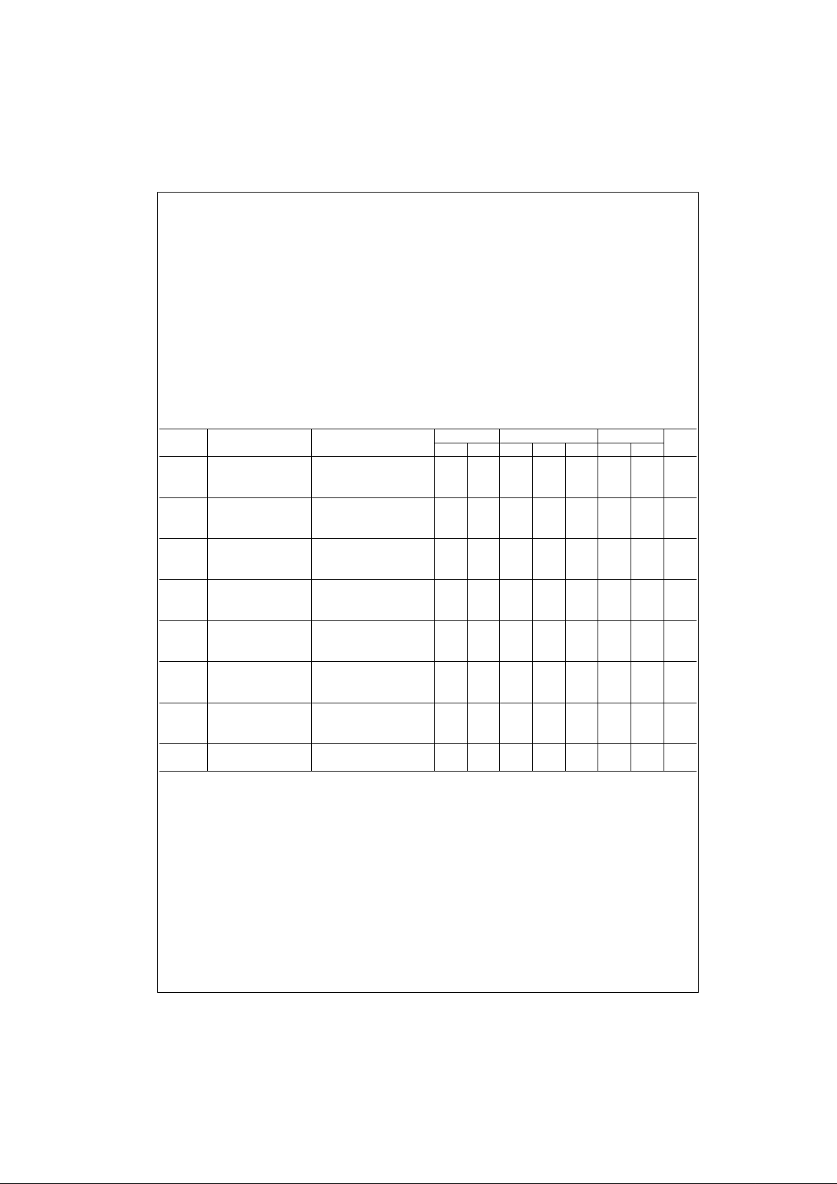
DC Electrical Characteristics (Note 3)
Note 3: VSS = 0V unless otherwise s pec if ied.
Note 4: I
OH
and IOL are tested one out put at a time.
DC Supply Voltage (VDD) −0.5 VDCto +18 V
DC
Input Voltage (VIN) −0.5 VDCto V
DD
+0.5 V
DC
Storage Temp. Range (TS) −65°C to +150°C
Power Dissipation (P
D
)
Dual-In-Line 700 mW
Small Outline 500 mW
Lead Temperature (T
L
)
(Soldering, 10 seconds) 260
°C
DC Supply Voltage (V
DD
)5 V
DC
to 15 V
DC
Input Voltage (VIN)0 V
DC
to VDD V
DC
Operating Temperature Range (TA) −40°C to +85°C
Symbol Parameter Conditions
−40°C +25°C +85°C
Units
Min Typ Min Typ Max Min Max
I
DD
Quiescent Device Current VDD = 5V 1.0 0.004 1.0 7.5
µAVDD = 10V 2.0 0.005 2.0 15
VDD = 15V 4.0 0.006 4.0 30
V
OL
LOW Level Output Voltage VDD = 5V 0.05 0 0.05 0.05
VVDD = 10V 0.05 0 0.05 0.05
VDD = 15V 0.05 0 0.05 0.05
V
OH
HIGH Level Output Voltage VDD = 5V 4.95 4.95 5 4.95
VVDD = 10V 9.95 9.95 10 9.95
VDD = 15V 14.95 14.95 15 14.95
V
IL
LOW Level Input Voltage VDD=5V, VO=4.5V 1.5 2 1.5 1.5
VVDD=10V, VO=9.0V |IO|<1µA 3.0 4 3.0 3.0
VDD=15V, VO=13.5V 4.0 6 4.0 4.0
V
IH
HIGH Level Input Voltage VDD=5V, VO=0.5V 3.5 3.5 3 3.5
VV
DD
=10V, VO=1.0V |IO|<1µA 7 .0 7.0 6 7.0
VDD=15V, VO=1.5V 11.0 11.0 9 11.0
I
OL
LOW Level Output Current VDD=5V, VO = 0.4V 0.52 0.44 0.88 0.36
mA(Note 4) V
DD
= 10V, VO = 0.5V 1.3 1.1 2.2 0.90
VDD = 15V, VO = 1.5V 3.6 3.0 8 2.4
I
OH
HIGH Level Output Current VDD = 5V, VO = 4.6V −0.52 −0.44 −0.88 −0.36
mA(Note 4) V
DD
= 10V, VO = 9.5V −1.3 −1.1 −2.2 −0.90
VDD = 15V, VO = 13.5V −3.6 −3.0 −8 −2.4
I
IN
Input Current VDD = 15V, VIN = 0V −0.3 −10−5−0.3 −1.0
µA
VDD = 15V, VIN = 15V 0.3 10−50.3 1.0
 Loading...