

Fairchild Semiconductor CD4022BCN, CD4022BCMX, CD4022BCM Datasheet
October 1987
Revised January 1999
CD4017BC • CD4022BC
Decade Counter/Divider with 10 Decoded Outputs •
Divide-by-8 Counter/Divider with 8 Decoded Outputs
CD4017BC • CD4022BC Decade Counter/Divider with 10 Decoded Outputs • Divide-by-8 Counter/Di vider with 8
Decoded Outputs
General Description
The CD4017BC is a 5- sta ge divi d e-by-10 J ohn son co unt er
with 10 decoded outputs and a carry out bit.
The CD4022BC is a 4-stage divide-by-8 Johnso n counter
with 8 decoded outputs and a carry-out bit.
These counters are cleared to their zero count by a lo gical
“1” on their reset line. These counters are advanced on the
positive edge of the clock signal when the clock enable signal is in the logical “0” state.
The configuration of the CD4 017BC and CD4022BC permits medium speed operation and assures a hazard free
counting sequence. The 10/8 decoded outputs are normally in the logical “0” st ate and go to the log ical “1” state
only at their respective time slot. Each decoded output
remains high for 1 full clock cycle. The carr y-out signal
completes a full cycle for every 10/8 clock input cycle s a nd
is used as a ripple carry signal to any succeeding stages.
Features
■ Wide supply voltage range: 3.0V to 15V
■ High noise immunity: 0.45 V
■ Low power Fan out of 2 driving 74L
TTL compatibility: or 1 driving 74LS
■ Medium speed operation: 5.0 MHz (typ.)
with 10V V
■ Low power: 10 µW (typ.)
■ Fully static operation
DD
DD
(typ.)
Applications
• Automotive
• Instrumentation
• Medical electronics
• Alarm systems
• Industrial electronics
• Remote metering
Ordering Code:
Order Number Package Number Package Description
CD4017BCM M16A 16-Lead Small Outline Integrated Circuit (SOIC), JEDEC MS-012, 0.150” Narrow
CD4017BCSJ M16D 16-Lead Small Outline Package (SOP), EIAJ TYPE II, 5.3mm Wide
CD4017BCN N16E 16-Lead Plastic Dual-In-Line Package (PDIP), JEDEC MS-001, 0.300” Wide
CD4022BCM M16A 16-Lead Small Outline Integrated Circuit (SOIC), JEDEC MS-012, 0.150” Narrow
CD4022BCN N16E 16-Lead Plastic Dual-In-Line Package (PDIP), JEDEC MS-001, 0.300” Wide
Devices also available in Tape and Reel. Specify by appending the suffix letter “X” to t he ordering code.
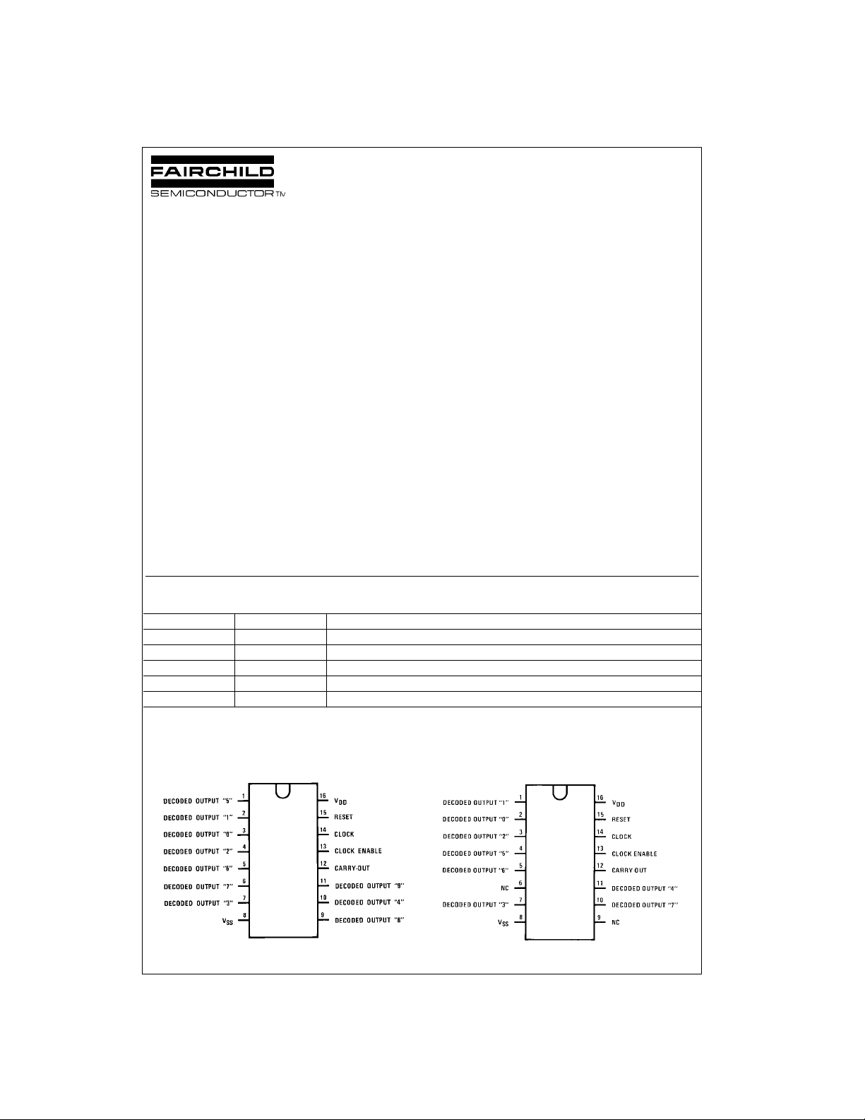
Connection Diagrams
Pin Assignments for DIP, SOIC and SOP
CD4017B
Top View
© 1999 Fairchild Semiconductor Corporation DS005950.prf www.fairchildsemi.com
Pin Assignments for DIP and SOIC
CD4022B
Top Vi ew
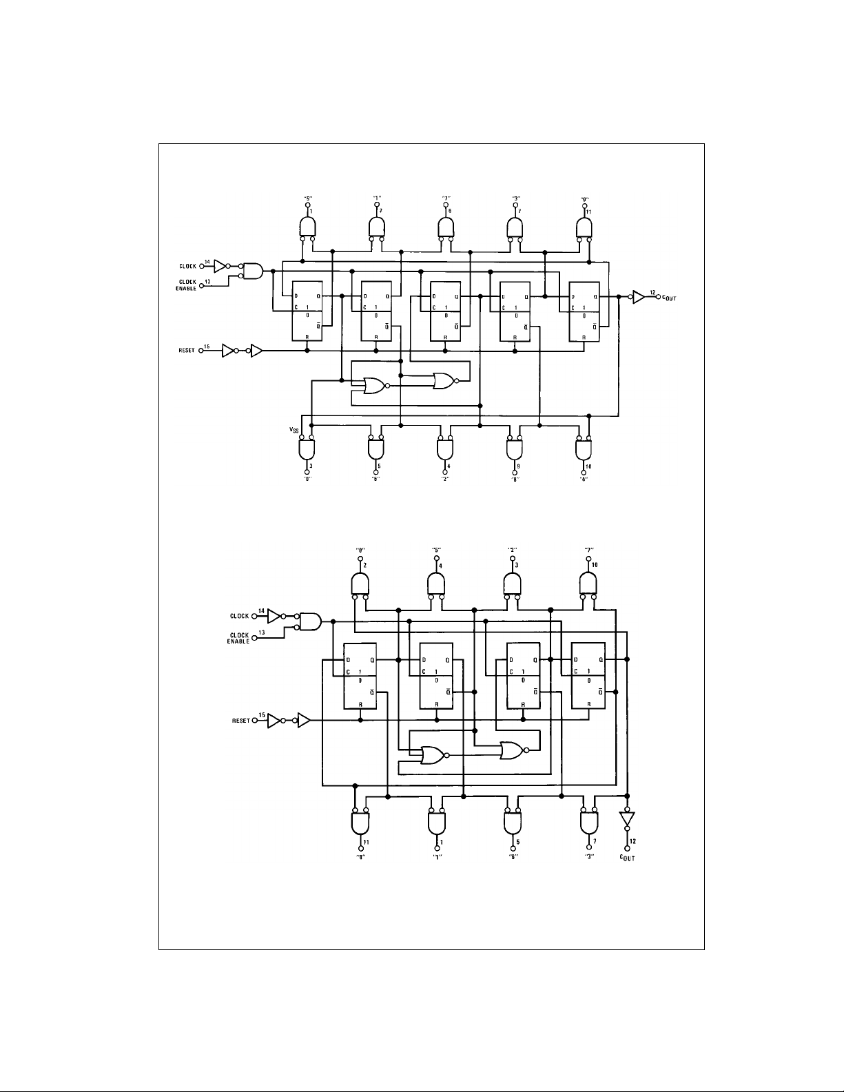
Logic Diagrams
CD4017BC • CD4022BC
Terminal No. 8 = GND
Terminal No. 16 = V
DD
CD4017B
CD4022B
Terminal No. 16 = V
Terminal No. 8 = GND
DD
www.fairchildsemi.com 2
Absolute Maximum Ratings(Note 1)
(Note 2)
DC Supply Voltage (VDD) −0.5 VDC to +18 V
Input Voltage (VIN) −0.5 VDC to VDD +0.5 V
Storage Temperature (TS) −65°C to +150°C
Power Dissipation (P
)
D
Dual-In-Line 700 mW
Small Outline 500 mW
Lead Temperature (T
)
L
(Soldering, 10 seconds ) 260°C
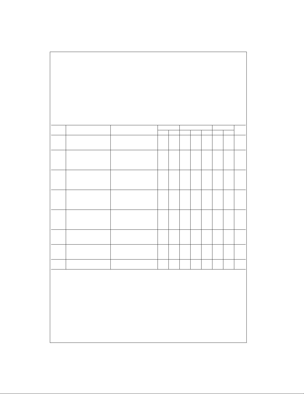
DC Electrical Characteristics (Note 2)
Symbol Parameter Conditions
I
V
V
V
V
I
I
I
Quiescent Device VDD = 5V 20 0.5 20 150 µA
DD
Current VDD = 10V 40 1.0 40 300 µA
LOW Level |IO| < 1.0 µA
OL
Output Voltage VDD = 5V 0.05 0 0.05 0.05 V
HIGH Level |IO| < 1.0 µA
OH
Output Voltage VDD = 5V 4.95 4.95 5 4.95 V
LOW Level |IO| < 1.0 µA
IL
Input Voltage VDD = 5V, VO = 0.5V or 4.5V 1.5 1.5 1.5 V
HIGH Level |IO| < 1.0 µA
IH
Input Voltage VDD = 5V, VO = 0.5V or 4.5V 3.5 3.5 3.5 V
LOW Level Output VDD = 5V, VO = 0.4V 0.52 0.44 0.88 0.36 mA
OL
Current (Note 3) VDD = 10V, VO = 0.5V 1.3 1.1 2.25 0.9 mA
HIGH Level Output VDD = 5V, VO = 4.6V −0.2 −0.16 −0.36 −0.12 mA
OH
Current (Note 3) VDD = 10V, VO = 9.5V −0.5 −0.4 −0.9 −0.3 mA
Input Current VDD = 15V, VIN = 0V −0.3 −10−5−0.3 −1.0 µA
IN
Note 3: IOL and IOH are tested one output at a ti m e.
VDD = 15V 80 5.0 80 600 µA
VDD = 10V 0.05 0 0.05 0.05 V
VDD = 15V 0.05 0 0.05 0.05 V
VDD = 10V 9.95 9.95 10 9.95 V
VDD = 15V 14.95 14.95 15 14.95 V
VDD = 10V, VO = 1.0V or 9.0V 3.0 3.0 3.0 V
VDD = 15V, VO = 1.5V or 13.5V 4.0 4.0 4.0 V
VDD = 10V, VO = 1.0V or 9.0V 7.0 7.0 7.0 V
VDD = 15V, VO = 1.5V or 13.5V 11.0 11.0 11.0 V
VDD = 15V, VO = 1.5V 3.6 3.0 8.8 2.4 mA
VDD = 15V, VO = 13.5V −1.4 −1.2 −3.5 −1.0 mA
VDD = 15V, VIN = 15V 0.3 10−50.3 1.0 µA
Recommended Operating
Conditions
DC Supply Voltage (V
DC
Input Voltage (VIN) 0 to VDD V
DC
Operating Temperature Range (TA) −40°C to +85°C
Note 1: “Absolute Maximum Rat ings” are tho se values beyond which the
safety of the device cannot be guaranteed, they are not meant to imply that
the devices should be operated at these limits. The table of “Recommended Operating Conditions” and “Electrical Characteristics” provides
conditions for actual device o peration.
= 0V unless otherw is e s pecified.
Note 2: V
SS
−40°C +25°+85°C
Min Max Min Typ Max Min Max
(Note 2)
) +3 VDC to +15 V
DD
CD4017BC • CD4022BC
DC
DC
Units
3 www.fairchildsemi.com
 Loading...