Fairchild Semiconductor CD4020BCC2, CD4019BCSJX, CD4019BCSJ, CD4019BCN, CD4019BCMX Datasheet
...
October 1987
Revised January 1999
CD4019BC Quad AND-OR Select Gate
© 1999 Fairchild Semiconductor Corporation DS005952.prf www.fairchildsemi.com
CD4019BC
Quad AND-OR Select Gate
General Description
The CD4019BC is a complementar y MOS quad AND-OR
select gate. Low power and high noise margin over a wide
voltage range is possible through implementation of N- and
P-channel enhancement m ode transistors. These comp lementary MOS (CMOS) transistors provide the building
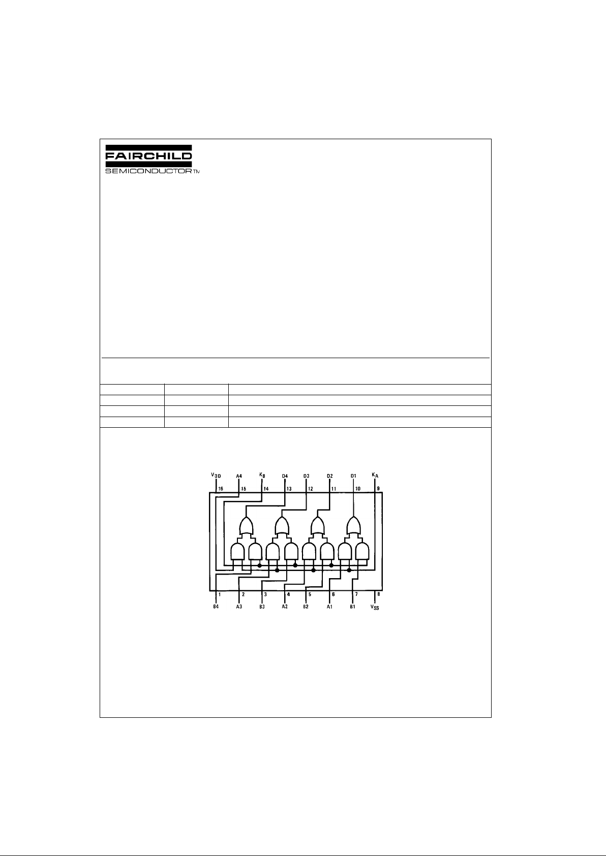
blocks for the 4 “AND-OR select” gate configuration s, each
consisting of two 2-input AND gates driving a single 2-input
OR gate. Selection is accompl ished by control bi ts K
A
and
K
B
. All inputs are protecte d against static discharge dam-
age.
Features
■ Wide supply voltage range: 3.0V to 15V
■ High noise immunity: 0.45 V
DD
(typ.)
■ Low power TTL compatibility: Fan out of 2 driving 74L
or 1 driving 74LS
Applications
• AND-OR select gating
• Shift-right/shift-left registers
• True/complement selection
• AND/OR/EXCLUSIVE-OR selection
Ordering Code:
Devices also available in Tape and Reel. Specify by appending the suffix letter “X” to t he ordering code.
Connection Diagram
Pin Assignments for DIP, SOIC and SOP
Top View
Order Number Package Number Package Description
CD4019BCM M16A 16-Lead Small Outline Integrated Circuit (SOIC), JEDEC MS-012, 0.150” Narrow
CD4019BCSJ M16D 16-Lead Small Outline Package (SOP), EIAJ TYPE II, 5.3mm Wide
CD4019BCN N16E 16-Lead Plastic Dual-In-Line Package (PDIP), JEDEC MS-001, 0.300” Wide

www.fairchildsemi.com 2
CD4019BC
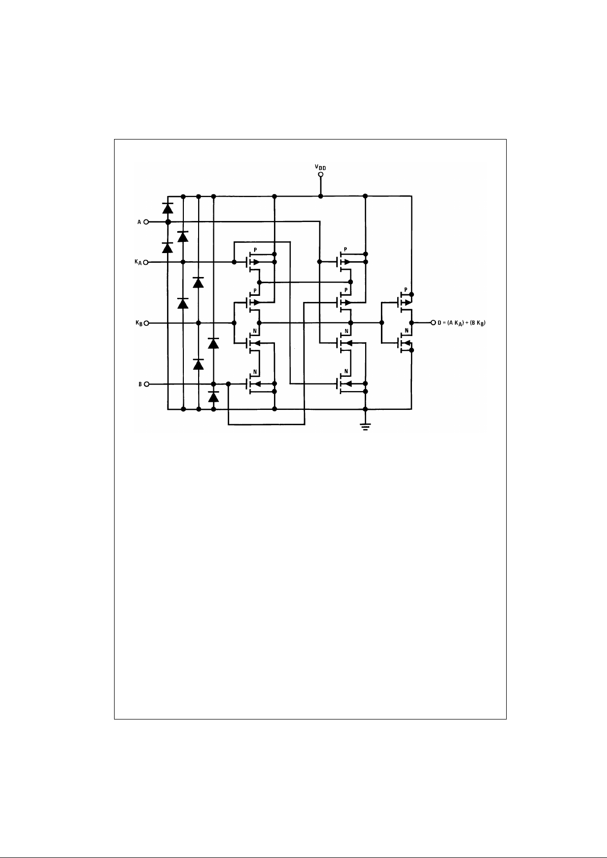
Schematic Diagram
Schematic diagram for 1 of 4 identical stages
 Loading...