

Fairchild Semiconductor BCW66G Datasheet
BCW66G
NPN General Purpose Amplifier
• This device is designed for general purpose amplifier applications at
collector currents to 500mA.
• Sourced from process 13.
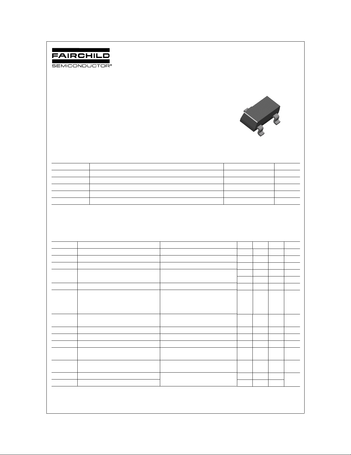
3
2
SOT-23
1
Mark: EG
1. Base 2. Emitter 3. Collector
BCW66G
Absolute Maximum Ratings * T
=25°C unless otherwise noted
C
Symbol Parameter Value Units
V
CEO
V
CBO
V
EBO
I
C
, T
T
J
STG
* These ratings are limiting values above which the serviceability of any semiconductor device may be impaired.
NOTES:
1. These ratings are based on a maximum junction temperature of 150degrees C.
2. These are steady state limits. The factory should be consulted on applications involving pulsed or low duty cycle operations.
Electrical Characteristics
Collector-Emitter Voltage 45 V
Collector-Base Voltage 75 V
Emitter-Base Voltage 5 V
Collector Current - Continuous 1 A
Operating and Storage Junction Temperature Range - 55 ~ +150 °C
TC=25°C unless otherwise noted
Symbol Parameter Test Condition Min. Typ. Max. Units
BV
CBO
BV
CEO
BV
EBO
I
CES
I
EBO
h
FE
(sat) Collector-Emitter Saturation Voltage IC = 100mA, IB = 10mA
V
CE
V
(sat) Base-Emitter Saturation Voltage IC = 500mA, IB = 50mA 2 V
BE
C
obo
C
ibo
f
T
Collector-Base Breakdown Voltage IC = 10µA75V
Collector-Emitter Breakdown Voltage IC = 10mA 45 V
Emitter-Base Breakdown Voltage IE = 10µA5V
Collector Cut-off Current VCB = 45V, IE = 0
= 45V, IE = 0
V
CB
= 150°C
T
A
20 nA
20 µA
Emitter Cut-off Current VEB = 4V 20 nA
DC Current Gain VCE = 10V, IC = 100µA
= 1V, IC = 10mA
V
CE
= 1V, IC = 100mA
V
CE
V
= 2V, IC = 500mA
CE
50
110
160
60
400
0.3
= 500mA, IB = 50mA
I
C
0.7
Output Capacitance VCB = 10V, f = 1MHz 12 pF
Input Capacitance VEB = 0.5V, f = 1MHz 80 pF
Current gain Bandwidth Product VCE = 10V, IC = 20mA,
100 MHz
f = 100MHz
NF Noise Figure V
= 5V, IC = 0.2mA, RS = 1kΩ,
CE
10 dB
f = 1KHz, BW = 200Hz
t
on
t
off
Turn-On Time IB1 = IB2 = 15mA
= 150mA, RL = 150Ω
I
Turn-Off Time 400
C
100 ns
V
©2002 Fairchild Semiconductor Corporation Rev. A1, August 2002

Thermal Characteristics
Symbol Parameter Min. Typ. Max. Units
P
D
R
θJA
Total Device Dissipation
Derate above 25°C
Thermal Resistance, Junction to Ambient 357 °C/W
350
2.8mWmW/°C
BCW66G
©2002 Fairchild Semiconductor Corporation Rev. A1, August 2002
 Loading...