

Page 1
e
SERVICE MANUAL
MODEL JP E3 E2 EK EA E1 E1K E1C
Ver. 7
Please refer to the
MODIFICATION NOTICE.
RCD-M39
RCD-M39DAB
P P P
P
CD RECEIVER
• The part list can be found in a separate le.See the part list in Excel format.
For purposes of improvement, specications and design are subject to change without notice.
•
Please use this service manual with referring to the operating instructions without fail.
•
Some illustrations using in this service manual are slightly different from the actual set.
•
e
D&M Holdings Inc.
S0603-0V07DM/DG1212
Copyright 2012 D&M Holdings Inc. All rights reserved.
WARNING: Violators will be prosecuted to the maximum extent possible.
Page 2

CONTENTS
ABOUT THIS MANUAL
What you can do with this manual ............................................3
Using Adobe Reader (Windows version) ..................................4
NOTE FOR SCHEMATIC DIAGRAM
Specications
CAUTION IN SERVICING
Initializing STEREO CD RECEIVER .......................................10
Support for Asia-Pacic tropical climate regions .....................10
DISASSEMBLY
About the photos used for "descriptions in the
DISASSEMBLY" section .........................................................12
1. LOADER PANEL ASSY .......................................................12
2. FRONT PANEL ASSY .........................................................13
3. CD MECHA .........................................................................14
4. HEAT SINK SUB ASSY .......................................................15
5. REAR PANEL ASSY ............................................................17
6. POWER UNIT ASSY ...........................................................19
7. MCU PCB UNIT ASSY ........................................................19
8. TRANS ................................................................................19
Note Handling and Replacement of the Laser pick-up
1. Protection of the LD .............................................................20
2. Precautions when handling the laser CD mechanism .........20
3. Cautions on assembling and adjustment ............................20
4. Determining whether the laser pick-up is defective .............20
Service Mode
How to input ...........................................................................21
1. Version display mode ..........................................................21
2. VFD checking mode ............................................................21
3. Cold start mode (initialization) .............................................22
4. CD test mode ......................................................................22
5. CD heat run mode ...............................................................26
6. Accumulated laser on time display mode ............................28
VERSION UPGRADE PROCEDURE OF FIRMWARE
1. ABOUT REPLACE THE MICROPROCESSOR
WITH A NEW ONE ..................................................................29
2. UPDATE MODE ..................................................................29
TROUBLE SHOOTING
1. VFD dosen't light .................................................................45
2. No Sound, Noise generated ................................................46
MEASURING METHOD AND WAVEFORMS
1. MCUCD PCB : TEST POINT ..............................................50
2. INPUT PCB : TEST POINT ................................................51
3. WAVEFORMS .....................................................................52
...........................................................................9
..........................................................................21
.............................................................3
.........................................7
........................................................10
........................................................................11
.......20
............29
............................................................45
..........................50
BLOCK DIAGRAM
CurrentBLOCK DIAGRAM
LEVEL DIAGRAM
WIRING DIAGRAM
PRINTED WIRING BOARDS
AMP ........................................................................................59
POWER ..................................................................................59
FRONT ...................................................................................60
SPEAKER ..............................................................................60
CONNECTOR ........................................................................61
CONNETER ...........................................................................61
CONNETER ...........................................................................61
MCU .......................................................................................62
DIGITAL INPUT ......................................................................63
DC-DC ....................................................................................63
REGULATOR .........................................................................63
DAB ........................................................................................63
SCHEMATIC DIAGRAMS (1/3)
MCU&CD ................................................................................64
DIGITAL INPUT .......................................................................65
POWER & AMP ......................................................................66
EXPLODED VIEW
EXPLODED VIEW OF CD MECHANISM UNIT
PARTS LIST OF EXPLODED VIEW
PARTS LIST OF CD MECHANISM UNIT
PACKING VIEW
PARTS LIST OF PACKING & ACCESSORIES
SEMICONDUCTORS
1. IC's ......................................................................................72
2. FL DISPLAY.........................................................................91
PARTS LIST OF PCB UNIT
...................................................................55
.....................................................56
....................................................................57
..................................................................58
...................................................59
...............................................64
...................................................................67
.......................68
.......................................69
...............................70
.......................................................................71
.......................71
...............................................................72
.....................................................94
2
Page 3
ABOUT THIS MANUAL
Read the following information before using the service manual.
What you can do with this manual
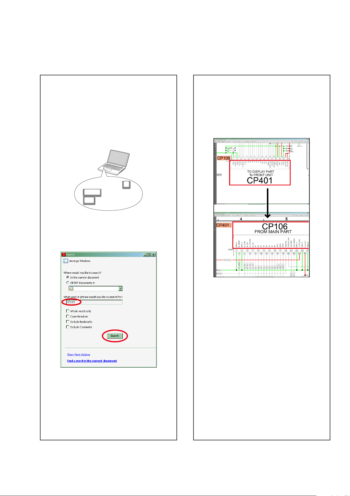
Search for a Ref. No. (phrase)
(Ctrl+Shift+F)
You can use the search function in Acrobat Reader to
search for a Ref. No. in schematic diagrams, printed
wiring board diagrams, block diagrams, and parts lists.
1.Press
2.Enter the Ref. No. you want to search for in the
Ctrl+Shift+F
on the keyboard.
• The Search window appears.
F
Shift
Ctrl
Search window, and then click the
• A list of search results appears.
Search
button.
Jump to the target of a schematic diagram
connector
Click the Ref. No. of the target connector in the red box
around a schematic diagram connector.
• The screen jumps to the target connector.
3.Click an item on the list.
• The screen jumps to the page for that item, and
the search phrase is displayed.
• Page magnification stays the same as before the
jump.
3
Page 4
Using Adobe Reader (Windows version)
Add notes to this data (Sign)
The Sign function lets you add notes to the data in this
manual.
Save the le once you have nished adding notes.
[Example using Adobe Reader X]
On the "
View
" menu, click "
• The Sign pane appears.
[Example using Adobe Reader 9]
On the "
Document
" menu, click "
Sign
".
Sign
".
Magnify schematic / printed wiring board
diagrams - 1
(Ctrl+Space, mouse operation)
Ctrl+Space
Press
mouse to select the area you want to view.
• The selected area is magnied.
• When you want to move the area shown, hold down
Space
and drag the mouse.
• When you want to show a full page view, press
Ctrl+0
on the keyboard.
on the keyboard and drag the
0
Ctrl Space
Print a magnied part of the manual
The Properties dialog box and functions will vary depending on your printer.
1. Drag the mouse to magnify the part you want to print.
2. On the "
File
" menu, click "
3. Congure the following settings in the Print dialog box.
Print
".
• Properties
Click this button and check that the printer is set to a
suitable paper size.
• Page to print
Select the following checkbox.
More Options
"
• Page Sizing & Handling
Select the following checkbox.
"
Size
Size Options
" / "
Current View
" : "
" : "
Fit
"
"
4. Click the
Print
button to start printing.
4
Page 5
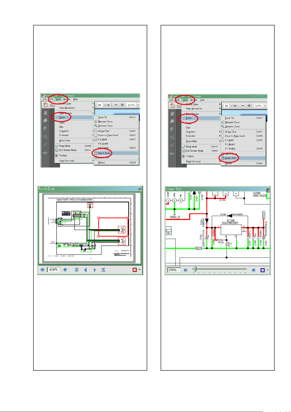
Magnify schematic / printed wiring board
diagrams - 2
(Pan & Zoom function)
The Pan & Zoom function lets you see which part of a
magnied diagram is being shown in a separate window.
Magnify schematic / printed wiring board
diagrams - 3
(Loupe Tool function)
The Loupe Tool function lets you magnify a specific
part of a diagram in a separate window.
[Example using Adobe Reader X]
On the "
Pan & Zoom
"
• The Pan & Zoom window appears on the screen.
View
" menu, point to "
".
Zoom
", and then click
[Example using Adobe Reader X]
On the "
Loupe Tool
"
• The Loupe Tool window appears on the screen.
View
" menu, point to "
".
Zoom
", and then click
[Example using Adobe Reader 9]
On the "
then click "
Tools
" menu, point to "
Pan & Zoom Window
Select & Zoom
[Example using Adobe Reader 9]
", and
".
On the "
then click "
5
Tools
" menu, point to "
Loupe Tool Window
Select & Zoom
".
", and
Page 6

SAFETY PRECAUTIONS
The following check should be performed for the continued protection of the customer and service technician.
LEAKAGE CURRENT CHECK
Before returning the unit to the customer, make sure you make either (1) a leakage current check or (2) a line to chassis
resistance check. if the leakage current exceeds 0.5 milliamps, or if the resistance from chassis to either side of the
power cord is less than 460 kohms, the unit is defective.
Be sure to test for leakage current with the AC plug in both polarities, in addition, in each power ON, OFF and STANDBY
mode, if applicable.
CAUTION
Please heed the points listed below during servicing and inspection.
◎Heed the cautions!
Spots requiring particular attention when servicing, such
as the cabinet, parts, chassis,etc., have cautions indicated
on labels. be sure to heed these causions and the
cautions indicated in the handling instructions.
◎Caution concerning electric shock!
(1) An AC voltage is impressed on this set, so touching
internal metal parts when the set is energized could
cause electric shock. Take care to avoid electric
shock, by for example using an isolating transformer
and gloves when servicing while the set is energized,
unplugging the power cord when replacing parts, etc.
(2) Tere are high voltage parts inside. Handle with extra
care when the set is energized.
◎ Caution concerning disassembly and
assembly!
Through great care is taken when manufacturing parts
from sheet metal, there may in some rare cases be burrs
on the edges of parts which could cause injury if ngers
are moved across them. Use gloves to protect your hands.
◎Only use designated parts!
The set's parts have specific safety properties (fire
resistance, voltage resistance, etc.). For replacement
parts, be sure to use parts which have the same
poroperties. In particular, for the important safety parts
that are marked z on wiring diagrams and parts lists, be
sure to use the designated parts.
◎ Be sure to mount parts and arrange the wires
as they were originally!
For safety seasons, some parts use tape, tubes or other
insulating materials, and some parts are mounted away
from the surface of printed circuit boards. Care is also
taken with the positions of the wores omsode amd clamps
are used to keep wires away from heating and high
voltage parts, so be sure to set everything back as it was
originally.
◎Inspect for safety after servicing!
Check that all screws, parts and wires removed or
disconnected for servicing have been put back in their
original positions, inspect that no parts around the area
that has been serviced have been negatively affected,
conduct an inslation check on the external metal
connectors and between the blades of the power plug,
and otherwise check that safety is ensured.
(Insulation check procedure)
Unplug the power cord from the power outlet, disconnect
the antenna, plugs, etc., and turn the power switch on.
Using a 500V insulation resistance tester, check that the
inplug and the externally exposed metal parts (antenna
terminal, headphones terminal, input terminal, etc.) is
1MΩ or greater. If it is less, the set must be inspected and
repaired.
CAUTION
Concerning important safety
parts
Many of the electric and structural parts used in the set
have special safety properties. In most cases these
properties are difficult to distinguish by sight, and using
replacement parts with higher ratings (rated power and
withstand voltage) does not necessarily guarantee that
safety performance will be poreserved. Parts with safety
properties are indicated as shown below on the wiring
diagrams and parts lists is this service manual. Be sure to
replace them with parts with the designated part number.
(1) Schematic diagrams ......Indicated by the z mark.
(2) Parts lists ......Indicated by the z mark.
Using parts other than the designated
parts could result in electric shock, res
or other dangerous situations.
6
Page 7

NOTE FOR SCHEMATIC DIAGRAM
NOTE FOR PARTS LIST
WARNING:
Parts indicated by the z mark have critical characteristics. Use ONLY replacement parts recommended by the manufacturer.
CAUTION:
Before returning the set to the customer, be sure to carry out either (1) a leakage current check or (2) a line to chassis resistance check. If
the leakage current exceeds 0.5 milliamps, or if the resistance from chassis to either side of the power cord is less than 460 kohms, the set
is defective.
WARNING:
DO NOT return the set to the customer unless the problem is identied and remedied.
NOTICE:
ALL RESISTANCE VALUES IN OHM. k=1,000 OHM / M=1,000,000 OHM
ALL CAPACITANCE VALUES ARE EXPRESSED IN MICRO FARAD, UNLESS OTHERWISE INDICATED. P INDICATES MICRO-MICRO
FARAD. EACH VOLTAGE AND CURRENT ARE MEASURED AT NO SIGNAL INPUT CONDITION. CIRCUIT AND PARTS ARE SUBJECT
TO CHANGE WITHOUT PRIOR NOTICE.
NOTE FOR PARTS LIST
1.
Parts for which "nsp" is indicated on this table cannot be supplied.
2.
When ordering of part, clearly indicate "1" and "I" (i) to avoid mis-supplying.
3.
Ordering part without stating its part number can not be supplied.
4.
Part indicated with the mark "★" is not illustrated in the exploded view.
5.
Not including General-purpose Carbon Film Resistor in the P.W.Board parts list. (Refer to the Schematic Diagram for those parts.)
6.
Not including General-purpose Carbon Chip Resistor in the P.W.Board parts list. (Refer to the Schematic Diagram for those parts.)
WARNING:
Parts marked with this symbol z have critical characteristics. Use ONLY replacement parts recommended by the manufacturer.
7
Page 8
m
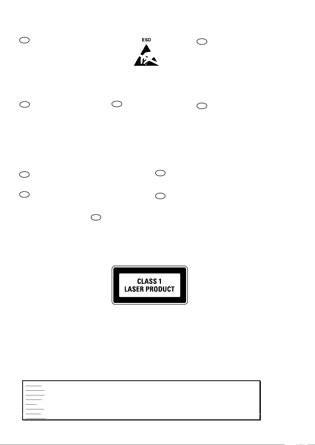
WARNING AND LASER SAFETY INSTRUCTIONS
GB
WARNING
All ICs and many other semi-conductors are
susceptible to electrostatic discharges (ESD).
Careless handling during repair can reduce
life drastically.
When repairing, make sure that you are
connected with the same potential as the
mass of the set via a wrist wrap with
resistance.
Keep components and tools also at this
potential.
F
ATTENTION
D
WARNUNG
I
WAARSCHUWING
AVVERTIMENTO
NL
Alle IC’s en vele andere halfgeleiders zijn
gevoelig voor elektrostatische ontladingen
(ESD).
Onzorgvuldig behandelen tijdens reparatie
kan de levensduur drastisch doen
verminderen.
Zorg ervoor dat u tijdens reparatie via een
polsband met weerstand verbonden bent met
hetzelfde potentiaal als de massa van het
apparaat.
Houd componenten en hulpmiddelen ook op
ditzelfde potentiaal.
Tous les IC et beaucoup d’autres semiconducteurs sont sensibles aux décharges
statiques (ESD).
Leur longévité pourrait être considérablement
écourtée par le fait qu’aucune précaution
n’est prise a leur manipulation.
Lors de réparations, s’assurer de bien être
relié au même potentiel que la masse de
l’appareil et enfiler le bracelet serti d’une
résistance de sécurité.
Veiller a ce que les composa
outils que l’on utilise soient également a ce
potentiel.
nts ainsi que les
GB
Safety regulations require that the set be restored to its original condition
and that parts which are identical with those specified be used.
NL
Veiligheidsbepalingen vereisen, dat het apparaat in zijn oorspronkelijke
toestand wordt terug gebracht en dat onderdelen, identiek aan de
gespecifieerde worden toegepast.
Alle IC und viele andere Halbleiter sind
empfindlich gegen elektrostatische
Entladungen (ESD).
Unsorgfältige Behandlung bei der Reparatur
kann die Lebensdauer drastisch vermindern.
Sorgen sie dafür, das Sie im Reparaturfall
über ein Pulsarmband mit Widerstand mit
dem Massepotential des Gerätes verbunden
sind.
Halten Sie Bauteile und Hilfsmittel ebenfalls
auf diesem Potential.
D
Bei jeder Reparatur sind die geltenden Sicherheitsvorschriften zu beachten.
Der Originalzustand des Gerats darf nicht verandert werden
Fur Reparaturen sind Original-Ersatzteile zu verwenden.
I
Le norme di sicurezza esigono che l’apparecchio venga rimesso nelle
condizioni originali e che siano utilizzati pezzi di ricambiago idetici a quelli
specificati.
Tutti IC e parecchi semi-conduttori sono
sensibili alle scariche statiche (ESD).
La loro longevita potrebbe essere fortemente
ridatta in caso di non osservazione della piu
grande cauzione alla loro manipolazione.
Durante le riparazioni occorre quindi essere
collegato allo stesso potenziale che quello
della massa dell’apparecchio tramite un
braccialetto a resistenza.
Assicurarsi che i componenti e anche gli
utensili con quali si lavora s
questo potenziale.
iano anche a
.
F
“Pour votre sécurité, ces documents
doivent être utilisés par des
spécialistes agrées, seu ls habilités à
réparer votre appareil en panne.”
Les normes de sécurité exigent que l’appareil soit remis a l’état d’origine et
que soient utilisées les pièces de rechange identiques à celles spécifiées.
LASER SAFETY
This unit employs a laser. Only a qualified service person should remove the cover or attempt to service t
device, due to possible eye injury.
his
USE OF CONTROLS OR ADJUSTMENTS OR PERFORMANCE OF PROCEDURE OTHER THAN THOSE
SPECIFIED H
EREIN MAY RESULT IN HAZARDOUS RADIATION EXPOSURE.
AVOID DIRECT EXPOSURE TO BEAM
WARNING
The use of optical instruments with this product will increase eye hazard.
Repair handling should take place as much as possible with a disc loaded inside the player
WARNING LOCATION: INSIDE ON LASER COVERSHIELD
CAUTION VISIBLE AND INVISIBLE LASER RADIATION WHEN OPEN AVOID EXPOSURE TO BEAM
ADVARSEL SYNLIG OG USYNLIG LASERSTRÅLING VED ÅBNING UNDGÅ UDS
ADVARSEL SYNLIG OG USYNLIG LASERSTRÅLING NÅR DEKSEL Å PNES UNNGÅ EKSPONERING FOR STRÅLEN
VARNING SYNLIG OCH OSYNLIG LASERSTRÅLNING NÄR DENNA DEL ÄR ÖPPNAD BETRAKTA EJ STRÅLEN
VARO! AVATT AESSA OLET ALTTIINA NÄKYVÄLLE JA NÄKYMÄTTÖMÄLLE LASER SÄ
VORSICHT SICHTBARE UND UNSICHTBARE LASERSTRAHLUNG WENN ABDECKUNG GEÖFFNET NICHT DEM STRAHL AUSSETSEN
DANGER VISIBLE AND INVISIBLE LASER RADIATION WHEN OPEN AVOID DIRECT EXPOSURE TO BEAM
ATTENTION RAYONNEMENT LASER VISIBLE ET INVISIBLE EN CAS D'OUVERTURE EXPOSITION DANGEREUSE AU FAISCEAU
Æ
TTELSE FOR STRÅLING
TEILYLLE. ÄLÄ KATSO SÄTEESEEN
030804ec
8
Page 9
SPECIFICATIONS
n Audio section
Power amplifer
Rated output:
30 W + 30 W (6 Ω, 1 kHz T.H.D 10 %)
n Tuner section
Receiving range (E2,EK model):
FM: 87.50 MHz – 108.00 MHz
DAB (EK model): BAND3 170 MHz – 240 MHz
Receiving range (E3 model):
FM: 87.50 MHz – 107.90 MHz
Usable sensitivity:
FM: 1.2 μV/75 Ω
DAB (EK model): –93 dBm/50 Ω
FM stereo separation: 35dB(1kHz)
n CD section
Playback frequency response: 2Hz ~ 20kHz
Wow & flutter: Below measurable limits (± 0.001%)
Sampling frequency: 44.1kHz
DIMENSION
n Clock/Timer section
Clock method: Crystal oscillator (Within 1 – 2 minutes per month)
Timer: Everyday/Once timer: One each
Sleep timer: 90 minutes, maximum
n General
Power supply (E2,EK model): AC 230 V, 50/60 Hz
Power supply (E3 model): AC 120 V, 60 Hz
Power consumption: 70 W
Approx. 0.3 W (standby)
25.0
129.1
130.0
210.0
152.0 29.029.0
30.0
272.0
8.5 106.5
11.0
308.0
115.0
199.045.0 28.0
9
Page 10
CAUTION IN SERVICING
Initializing STEREO CD RECEIVER
STEREO CD RECEIVER initialization should be performed when the μcom, peripheral parts of μcom, and Digital PCB.
are replaced.
1. Turn off the power using "Power operation (X)" button, unplug the power cord.
2. Plug the power cord into a power outlet while pressing "8 / –" and "SOURCE" button simultaneously.
Initialize.
*
NOTE: All user settings will be lost and this factory setting will be recovered when this initialization mode.
So make sure to memorize your setting for restoring after the initialization.
8 / -
Power operation (X) SOURCE
Support for Asia-Pacic tropical climate regions
Before selling this product, purchase and attach the tropical standard supporting part.
For this part, see the part list on page 67.
For where to attach the part, see the exploded view.
10
Page 11
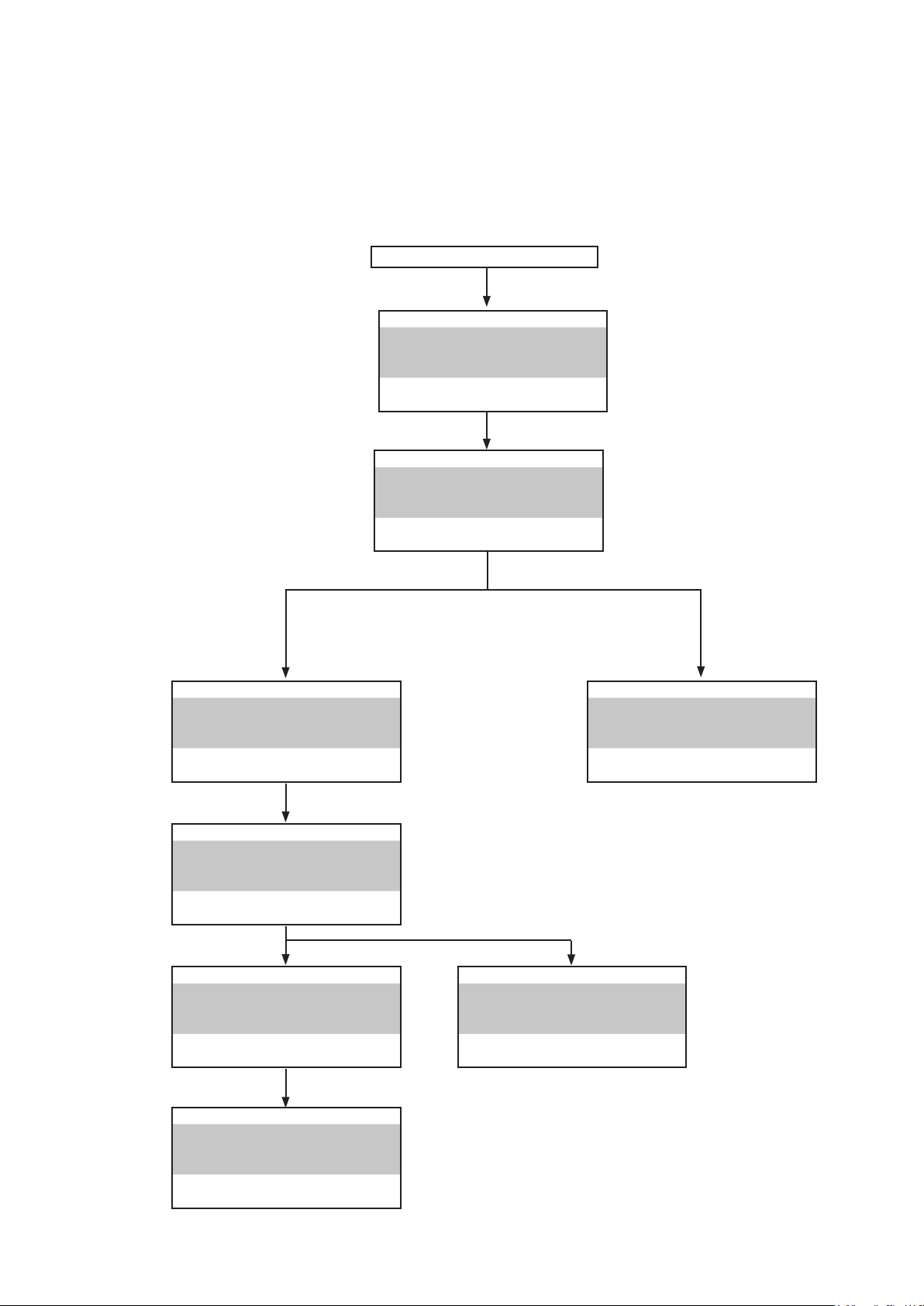
DISASSEMBLY
• Disassemble in order of the arrow of the gure of following ow.
• In the case of the re-assembling, assemble it in order of the reverse of the following ow.
• In the case of the re-assembling, observe "attention of assembling" it.
• If wire bundles are untied or moved to perform adjustment or parts replacement etc., be sure to rearrange them neatly
as they were originally bundled or placed afterward.
Otherwise, incorrect arrangement can be a cause of noise generation.
TOP COVER
LOADER PANEL ASSY
"DISASSEMBLY
Refer to
1. LOADER PANEL ASSY"
"EXPLODED VIEW"
and
LOADER PANEL
(Ref. No. of EXPLODED VIEW : 3)
FRONT PANEL ASSY
"DISASSEMBLY
Refer to
2. FRONT PANEL SUB ASSY"
"EXPLODED VIEW"
and
FRONT PANEL
(Ref. No. of EXPLODED VIEW : 6)
HEAT SINK SUB ASSY
"DISASSEMBLY
Refer to
4. HEAT SINK SUB ASSY"
"EXPLODED VIEW"
and
HEAT SINK
(Ref. No. of EXPLODED VIEW : 18)
REAR PANEL ASSY
"DISASSEMBLY
Refer to
5. REAR PANEL ASS'Y"
"EXPLODED VIEW"
and
REAR PANEL
(Ref. No. of EXPLODED VIEW : 21)
POWER UNIT ASSY
"EXPLODED VIEW"
Refer to
6. POWER UNIT ASS'Y"
"EXPLODED VIEW"
and
POWER UNIT
(Ref. No. of EXPLODED VIEW : P1)
TRANS
"EXPLODED VIEW"
Refer to
8. TRANS"
"EXPLODED VIEW"
and
TRANS
(Ref. No. of EXPLODED VIEW : P6)
Refer to
and
CD MECHA
(Ref. No. of EXPLODED VIEW : P8)
MCU PCB UNIT ASSY
"EXPLODED VIEW"
Refer to
7. MCU PCB UNIT ASSY"
"EXPLODED VIEW"
and
MCU PCB UNIT
(Ref. No. of EXPLODED VIEW : P3)
CD MECHA ASS'Y
"DISASSEMBLY
3. CD MECHA ASS'Y"
"EXPLODED VIEW"
11
Page 12
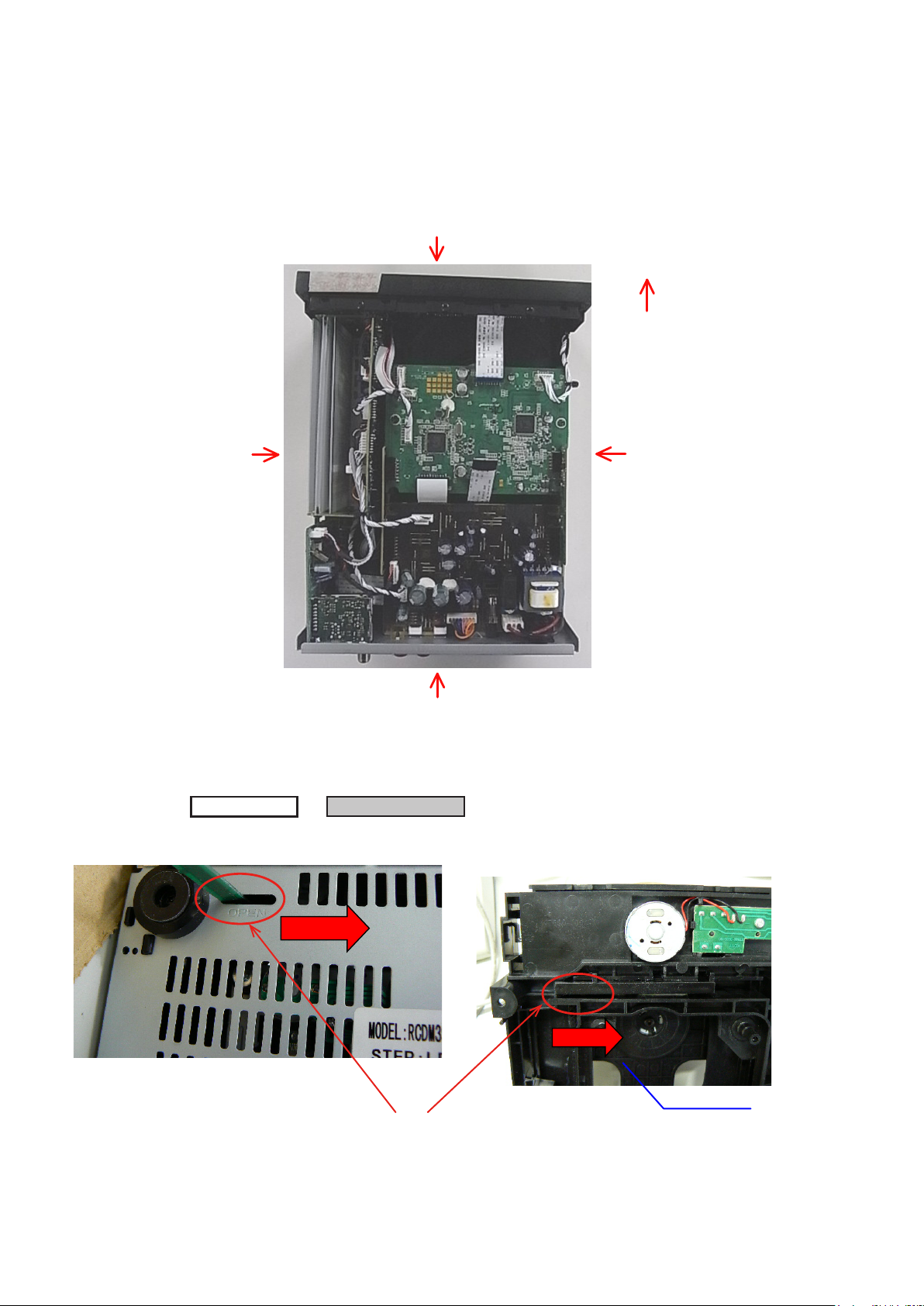
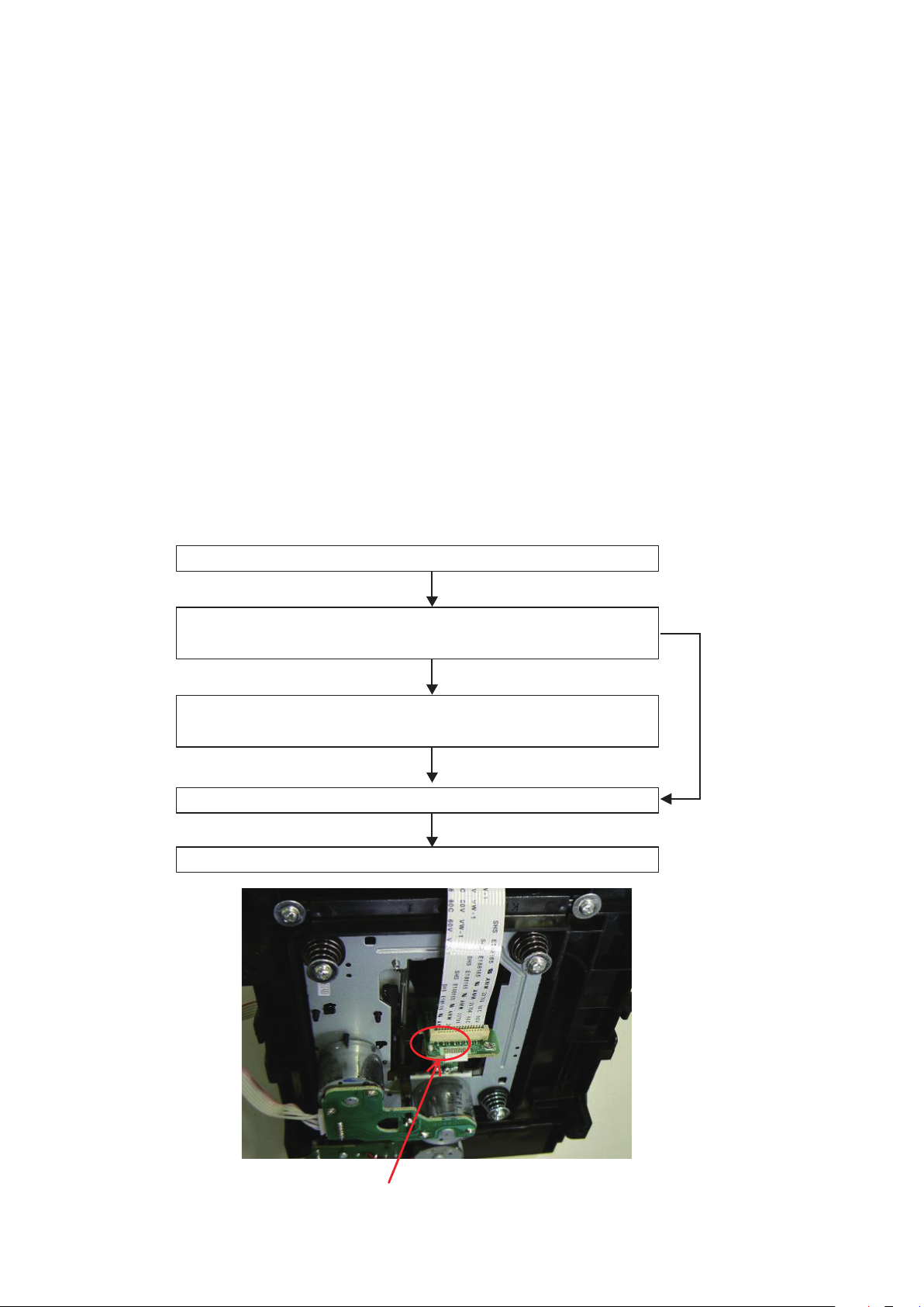
About the photos used for "descriptions in the DISASSEMBLY" section
• The direction from which the photographs used herein were photographed is indicated at "Direction of photograph: ***"
at the left of the respective photographs.
• Refer to the table below for a description of the direction in which the photos were taken.
• Photographs for which no direction is indicated were taken from above the product.
• The photograph is RCD-M39 model.
The viewpoint of each photograph
(Photografy direction)
[View from above]
Direction of photograph: C
Direction of photograph: B
Front side
Direction of photograph: D
1. LOADER PANEL ASSY
Proceeding : TOP COVER
(1) Detach the LOADER PANEL.
You can slide in the arrow direction to pull out the TRAY.
Direction of photograph: A
LOADER PANEL
→
CD MECHA
12
Page 13
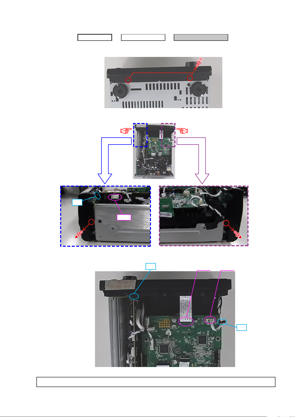
2. FRONT PANEL ASSY
Proceeding : TOP COVER
(1) Remove the screws.
View from bottom
(2) Disconnect the connector wire, then remove the screws.
Direction of
photograph: C
LOADER PANEL
→
FRONT PANEL ASSY
→
Direction of
photograph: D
cut
CWAJ
(3) Cut the wire clamp band, then disconnect the connector wires.
cut
Direction of photograph: B
CWMF FCMA
cut
Please refer to "EXPLODED VIEW" for the disassembly method of each PCB included in FRONT PANEL ASSY.
13
Page 14
3. CD MECHA
Proceeding : TOP COVER
CD MECHANISM ASS'Y
→
(1) Remove the screws.
Direction of photograph: D
(2) Pull out the TRAY.
LOADER PANEL
→
FRONT PANEL ASS'Y
→
You can slide in the arrow direction to pull out the TRAY.
(3) Cut the wire clamp band, then disconnect the connector wires. Remove the screws.
PMSN
Direction of photograph: B
PMMO
CD MECHA
PMUP
FCMC
CMMD
14
cut
Page 15
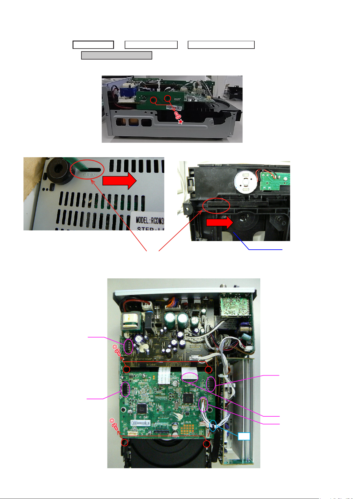
4. HEAT SINK SUB ASSY
Proceeding : TOP COVER
HEAT SINK SUB ASSY
→
(1) Cut the wire clamp band, then disconnect the connector wires.
Direction of photograph: B
LOADER PANEL
→
→
FRONT PANEL ASS'Y
CWSQ
CWIL
CBSK
cut
(2) Remove the screws.
Direction of photograph: C
CMMD
cut
15
Page 16
(3) Remove the screws.
View from bottom
(4) Disconnect the connector wires.
CBAM
Direction of photograph: C
HEAT SINK SUB ASSY
Please refer to "EXPLODED VIEW" for the disassembly method of each PCB included in HEAT SINK SUB ASSY.
16
Page 17
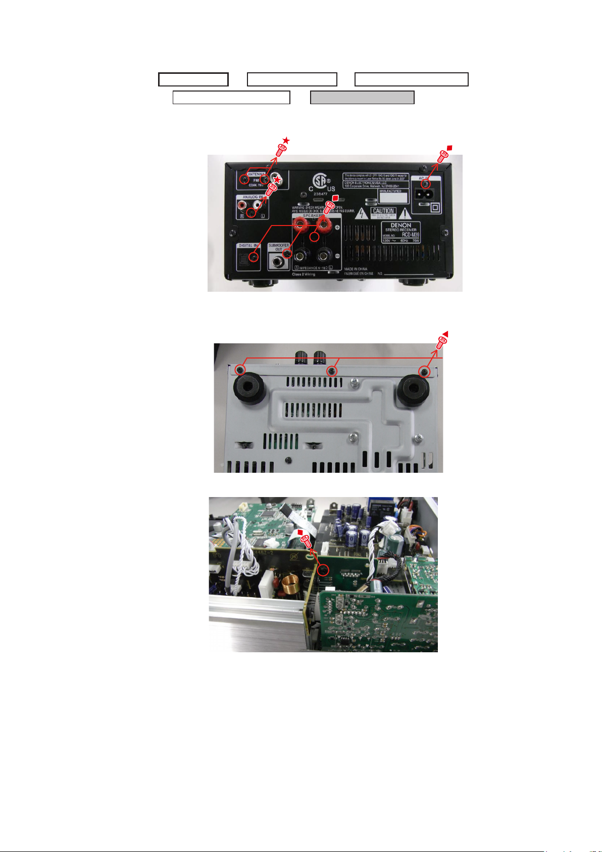
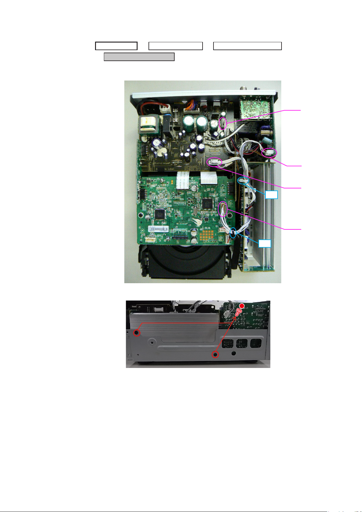
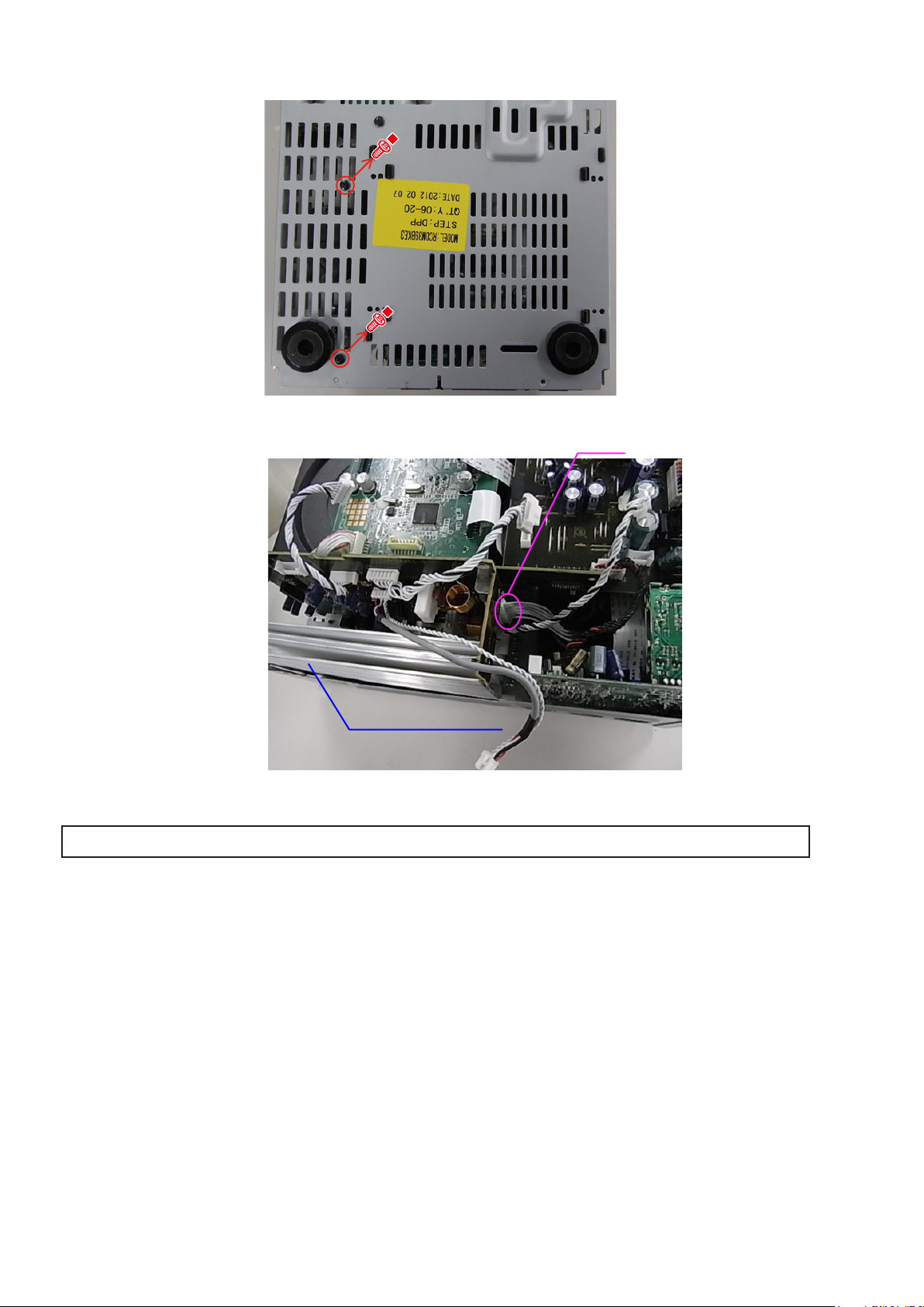
5. REAR PANEL ASSY
Proceeding : TOP COVER
HEAT SINK SUB ASSY
→
(1) Remove the screws.
Direction of photograph: A
(2) Remove the screws.
LOADER PANEL
→
FRONT PANEL ASS'Y
→
REAR PANEL ASSY
→
View from bottom
(3) Remove the screws.
Direction of photograph: C
17
Page 18
(4) Disconnect the connector wire, then remove the screws.
CN91
PMSE
Direction of photograph: B
FCMC
(5) Remove the screws.
Direction of photograph: D
Please refer to "EXPLODED VIEW" for the disassembly method of each PCB included in REAR PANEL SUB ASSY.
18
Page 19
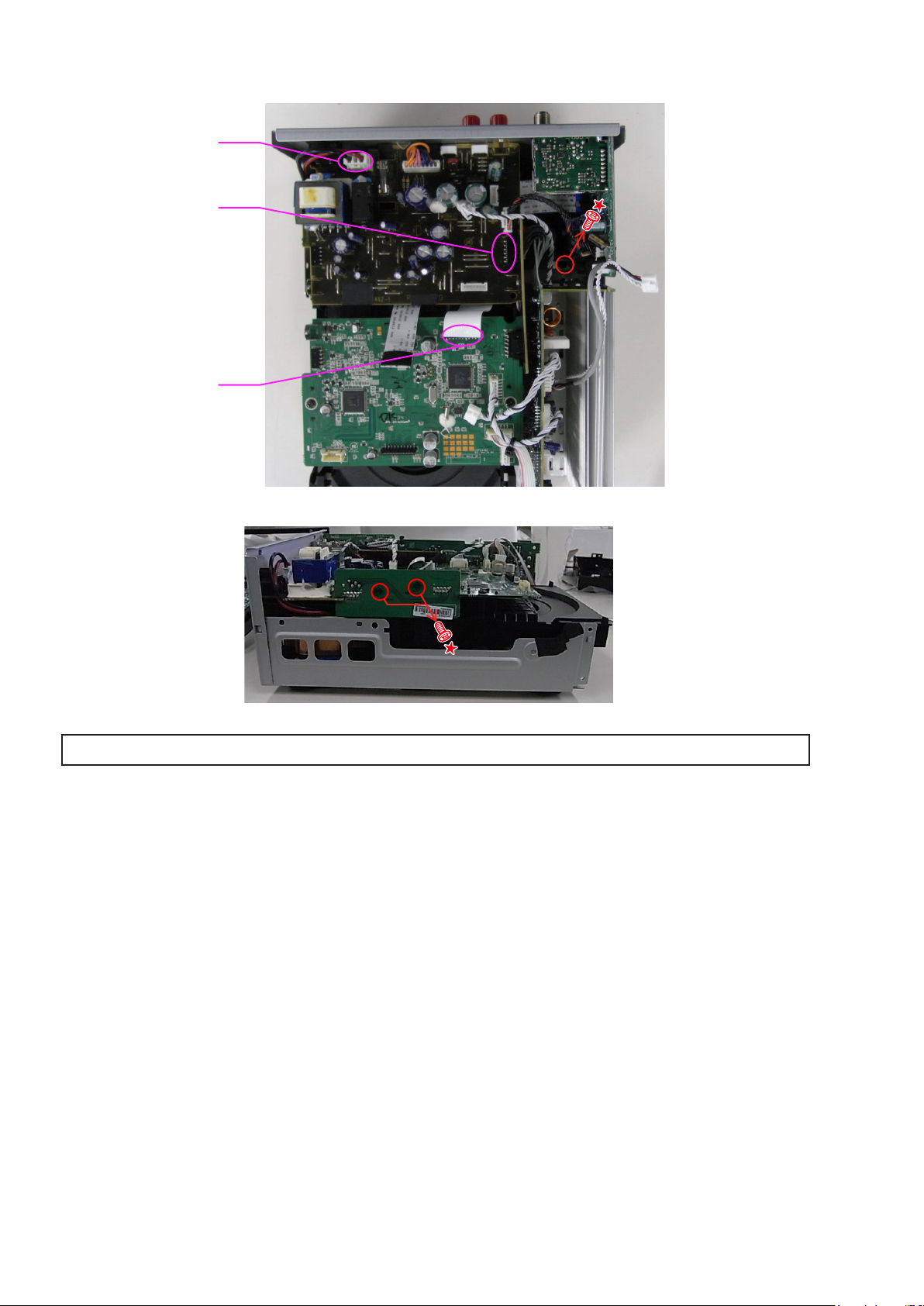
6. POWER UNIT ASSY
→
Proceeding : TOP COVER
HEAT SINK SUB ASSY
→
Please refer to "EXPLODED VIEW" for the disassembly method of POWER UNIT.
LOADER PANEL
→
REAR PANEL ASSY
→
FRONT PANEL ASS'Y
→
7. MCU PCB UNIT ASSY
Proceeding : TOP COVER
HEAT SINK SUB ASSY
→
Please refer to "EXPLODED VIEW" for the disassembly method of MCU PCB UNIT.
LOADER PANEL
→
REAR PANEL ASSY
→
FRONT PANEL ASS'Y
→
8. TRANS
Proceeding : TOP COVER
HEAT SINK SUB ASSY
→
TRANS
LOADER PANEL
→
REAR PANEL ASSY
→
FRONT PANEL ASS'Y
→
POWER UNIT ASSY
→
MCU PCB UNIT ASSY
→
POWER UNIT ASSY
→
Please refer to "EXPLODED VIEW" for the disassembly method of TRANS.
19
Page 20
NOTE HANDLING AND REPLACEMENT OF THE LASER PICK-UP
1. Protection of the LD
Short a part of the LD circuit by soldering. After connection to a circuit, remove the short solder.
2. Precautions when handling the laser CD mechanism
• Handle the laser pick-up so that it is not exposed to dust.
• Do not leave the laser pick-up bare. Be sure to cover it.
• If dust adheres on lens of the pick-up, blow it off with a blower brush.
• Do not shock the laser pick-up.
• Do not watch the light of the laser pick-up.
3. Cautions on assembling and adjustment
• Be sure that to the bench, jig, head of soldering iron (with ceramic) and measuring instruments are well grounded.
• Workers who handle the laser pick-up must be grounded.
• The nished mechanism (prior to anchoring in the set) should be protected against static electricity and dust. The
mechanism must be stored that damaging outside forces are not received.
• When carrying the nished mechanism, hold it by the chassis body
• For proper operation, storage and operating environment should not contain corrosive gases. For example H2S, SO2,
NO2, CI2 etc. In addition storage environment should not have materials that emit corrosive gases especially from
silicic, cyanic, formalin and phenol group. I the mechanism or the set, existence of corrosive gases may cause no
rotation in motor.
4. Determining whether the laser pick-up is defective
Disc no read, unsteady playback, etc.
Measure the waveform at RFO on "MCU CD PCB wRFO".
(For measuring points and waveforms, Rrfer to 50 page.)
Range between 0.4 and 1.1(Vp-p)
Laser drive current (Iop) check
(For how to check, see 4. CD test mode, 4.7.Laser current is display.)
Laser current (IOP) memorizing after replacement
Present value exceeds the initial value
by 1.5 times
Traverse Unit replacing
NO
Protective soldering place for laser diode.
20
Page 21
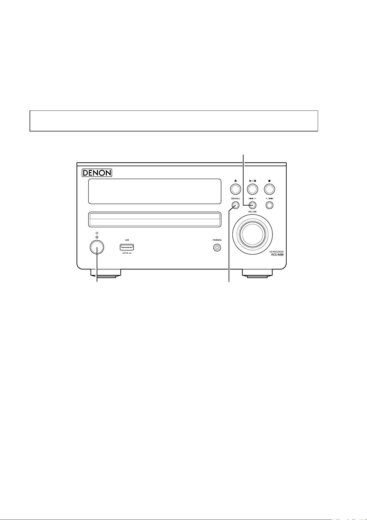
SERVICE MODE
How to input
Plug AC cord into power outlet while pressing both the button A and the button B at the same time.
No. Mode Button A Button B
1 Version display mode
2 VFD checking mode
3 Cold start mode (initialization) SOURCE
4 CD test mode SOURCE
5 CD heat run mode
6 Accumulated laser on time display mode
7 Displaying the protection history mode SOURCE
2 8
5
2
2
Power operation (X)
Power operation (X)
Power operation (X)
1. Version display mode
(1) Plug AC cord into power outlet while pressing "2" and "8 / –" button same time on Main Unit.
(2) Press the "SDB/TONE" button to the display the 2nd item information on the Display.
Main µ-com Ver.】→【USB µ-com Ver.】→【Main µ-com Ver.】→
【
Main µ-com Ver.
【
】
V e r 1 2 0 6 0 8 0 2 v E 2
8
+ /
+ /
/ –
/ –
9
9
・・・
USB µ-com Ver.
【
】
U S B V E R
2 0 1 2 0 5 2 4 0 1
(3) Unplug AC cord to clear this mode.
2. VFD checking mode
(1) Plug AC cord into power outlet while pressing "Power operation (X)" and "5" button same time on Main Unit.
(2) All segment of VFD is turning on and off every one second. MUTING ON
(3) Unplug AC cord to clear this mode.
.
21
Page 22
3. Cold start mode (initialization)
(1) Plug AC cord into power outlet while pressing "SOURCE" and "8 / -" button same time on Main Unit.
Initialize.
I N I T I A L I Z E
Default
SOURCE DISC
TUNER BAND EK:DAB, otherFM
TUNER frequency Minimum reception frequency
TUNER PRESET 0
Set -/+ PRESET
SDB OFF
BASS 0
TREBLE 0
BLANCE CENTER
DIMMER 100%
VOLUME 8
Clock E3:AM12:00, Other:0:00
ALARM SOURCE DISC
ALARM ON E3:AM12:00, Other:0:00
ALARM OFF E3:AM12:00, Other:0:00
SPK OPTIMISE ON
iPod MODE REMOTE
AUTO STANDBY E2/EK:ON, E3:OFF
DAB Module (EK) Initialzed Module
Protection memory NO PROTECT
The following settings are not initialized.
※
• Laser ON TIME and Laser Current
• Power supply abnormal ag
(2) After initialization, the unit will start in normal mode (Power On).
4. CD test mode
(1) Plug AC cord into power outlet while pressing "Power operation (X)" and "SOURCE" button same time on Main Unit.
" 1 3 "
0 0 C D T E S T M O D E
(2) Move the slide to the initially set position (10 mm towards the outside from the innermost position).
(3) Check by performing key input. Refer to 4.2
q
~
4.2y.
(4) Cancel the mode by turning the power back on.
Do not push the button without the explanation.
※
4.1 Disc loading
(1) Press the "5" button to open the tray.
(2) Set a disc on the tray, then press the "5" button again to close the tray.
(3) Move the slide to the initially set position (10 mm towards the outside from the innermost position) and stop in this
status.
(
1, 3
ashing
)
22
Page 23
4.2 Servo check
• Press the "5" button. Execute the following steps.
Press "1/3" button continuously for over 1second to switch directly to SUB CODE readout in step t.
※
LD ON (with servo still stopped)
q
" 1 3 "
0 1 L D O N
FOCUS ON (disc rotation, tracking off)
w
If no disc loaded, retry then stop.
z
" 1 3 "
0 2 F o c u s O N
CLV ON
e
" 1 3 "
0 3 C L V O N
TRACKING ON
r
" 1 3 "
(
1, 3
(
1, 3
(
1, 3
ashing
ashing
ashing
)
)
)
0 4 T r a c k i n g O N
SUB CODE readout (playback sound output)
t
" 1 3 "
0 5 @ @
When display is as in t and the "1/3" button is pressed, conduct BER (Block Error Rate) display for 2 seconds.
y
" 1 3 "
Tr
ashing / @@:T.No / XX:XX:Time
(
1, 3
X X : X X
(
1, 3
ashing
)
)
E R R # # # # # #
ashing / ######:B.E.R
(
1, 3
)
23
Page 24
4.3 Pickup movement
(1) In the stop mode, pickup moves in REV (inwards) or FWD (outwards) direction when "8 / -" or "+ / 9" button
pressed.
(2) When "8 / -" button pressed, move to stop operation after detection that inner switch has turned on.
(3) Pickup movement stops when button released.
4.4 Stop
(1) When "2" button is pressed, play operation and servo stop.
(2) After stopping, conduct reading of auto adjust values.
4.5 All servo on
• Press and hold the "SOURCE" button for 5 seconds and longer to turn on all servos. The system is automatically
adjusted and the playback operation starts. (Playback sound output)
" 1 3 "
@ @
Tr
ashing / @@:T.No / XX:XX:Time
(
1, 3
X X : X X
)
4.6 Adjustment value display
(1) When "DIRECT" button is pressed, the adjustment values are displayed in the following order.
FOCUS BALANCE
q
" 1 3 "
X X X X
F O C U S B A L A N C E
FOCUS GAIN
w
" 1 3 "
ashing / XXXX:Adjustment value
(
1, 3
)
X X X X
F O C U S G A I N
TRACKING BALANCE
e
" 1 3 "
ashing / XXXX:Adjustment value
(
1, 3
)
X X X X
T R A C K I N G B A R A N C E
TRACKING GAIN
r
" 1 3 "
ashing / XXXX:Adjustment value
(
1, 3
)
X X X X
T R A C K I N G G A I N
FOCUS OFFSET
t
" 1 3 "
ashing / XXXX:Adjustment value
(
1, 3
)
X X X X
F O C U S O F F S E T
TRACKING OFFSET
y
" 1 3 "
ashing / XXXX:Adjustment value
(
1, 3
)
X X X X
T R A C K I N G O F F S E T
ashing / XXXX:Adjustment value
(
1, 3
)
24
Page 25
RFRP
u
" 1 3 "
X X X X
R F R P
2) Press the "2" button, "4. CD test mode (1)" display reappears.
(
If auto adjustment is not completed, proper values are not displayed.
※
4.7 Laser current is display
(1) When the "2" button is pressed for over 1 second while the RCD-M39 is in the stop mode(Display of "4. CD test
mode (1)"), the laser turns on and the laser current is measured.
" 1 3 "
ashing / XXXX:Adjustment value
(
1, 3
)
S / C : X X m A / Y Y m A
L A S E R C U R R E N T
• The rst current value is measured 3 seconds after the laser turns on.
• The current value is updated every 3 seconds.
• The laser drive current undergoes A/D conversion for calculation. Decimal values are discarded.
2) Press the "2" button, "4. CD test mode (1)" display reappears.
(
ashing / XX:Stored data(stored in the EEPROM) / YY:Current value
(
1, 3
Stored data is not cleared, initialazation of "3. Cold start mode".
※
)
4.7.1 Overwriting the stored data
(1) When the "1/3" button is pressed for over 5 seconds while the laser current is displayed, the current value is
stored in the EEPROM (overwriting the stored data).
" 1 3 "
S T O R E D
L A S E R C U R R E N T
(2) Press the "
(3) Once rewriting is completed, the display in No.4.7(1) reappears.
Rewriting is performed upon shipment from the factory and when the mechanism is replaced.
※
" button, the initial value is stored in the EEPROM.
1/3
(
1, 3
ashing
)
25
Page 26
5. CD heat run mode
(1) Plug AC cord into power outlet while pressing "2" and "+ / 9" button same time on Main Unit. (Be sure to insert
the CD before this operation)
1
3
C D 1 1
(
1, 3
Tr
lit / Normal display except when 1, 3 lit
4 2 : 5 2
.)
(2) Switches to mode according to button input. See No.5.1 and No.5.2.
(3) If an error occurs, display the error and stop operation at that point. Number of operations held. See No.5.3 to
No.5.5.
(4) Heat run no. cleared when "2" button pressed.
(5) Mode canceled and tray opened after "5" button pressed.
(6) Press the "Power operation (X)" button to clear this mode too.
5.1 Normal heat run mode
• After CD heat run mode has started, re-read TOC and press the "1/3" button. (Be sure to nish reading the TOC
before push "1/3" button) Count this as the 0th heat run repetition.
Play from the rst to last track on disc.
q
If disc being used has less than 20 tracks, play all tracks. If disc has 21 or more tracks, skip to nal track after
w
playback of rst track has nished.
After disc playback has nished, move pickup to innermost position and open tray.The heat run repetition no. is
e
incremented (increased by 1) when the tray is opened.
When loader open status detected, close tray again, re-read TOC and start playback from the rst track on the
r
disc.
Conduct q to r repeatedly.
t
During playback is display
【
1
3
】
C D 0 1
Number of heat run is display (No.5.1 e)
【
1
3
(
1, 3
Tr
lit / Normal display except when 1, 3 lit
0 1 : 4 7
】
.)
C D X X X X
5.2 Automatic mounting mode
(1) After CD heat run mode has started, re-read TOC and press the "2" buton once in the stop mode.
(2) TOC reading ⇒ Search for rst track on disc ⇒ tray open ⇒ tray close ⇒ TOC reading ⇒ repeat. No. heat run
repetitions displayed on time display section.
(3) Increment the heat run repetition no. at the point when the loader has nished opening.
When the tray is open
【
1
3
】
lit / XXXX:No. of heat run repetitions
(
1, 3
)
C D X X X X
When the tray is closed
【
1
3
】
lit / XXXX:No. of heat run repetitions
(
1, 3
)
C L O S E
26
(
1, 3
lit
)
Page 27
When TOC is read
【
1
3
】
R E A D I N G
(
5.3 Error display
1
3
1, 3
lit)
C D E X - X X
Error code
E1-00 Disc cannot be detected
E1-01 Tracking offset adjustment not possible
E1-02 Focus offset adjustment not possible
E2-00 Focus servo dropped during playback.
E2-01 Focus servo dropped during searching.
E2-03 Focus servo dropped during TOC reading.
E2-06 Focus servo dropped during manual search.
E2-10 Subcode can no longer be read during playback
E2-11 Subcode can no longer be read during searching
E2-12 Subcode can no longer be read during TOC reading
E2-14 Subcode cannot be read during pause
E2-15 Subcode cannot be read during manual search
lit / X-XX:Error cord
(
1, 3
)
E3-00 TOC could not be read within specied time
E3-01 PVD/SVD analysis could not be completed within specied time
E4-04 Search time out
E4-05 Error in communications with CD decoder
E5-00 Inner switch not on
E6-00 Inner switch not off
E9-00 Tray is not opened by the specied time.
E9-01 Other error
Number of heat runs performed when error occurred
【
】
(1) Press the "+/9" button while the error is displayed.
(2) No. heat runs is displayed for 5 seconds, the error display reappears.
1
3
C D X X X X
【
lit / XXXX:Number of heat runs repeated when error occurred
(
1, 3
Track no. and elapsed time when error occurred
】
)
(1) Press the "8/ -" button while the error is displayed.
(2) The track no. and time when the error occurred is displayed for 5 seconds, then error display reappears.
1
3
C D 0 1
lit / mm:ss:Number of heat runs repeated when error occurred
(
1, 3
Tr
m m : s s
)
27
Page 28

6. Accumulated laser on time display mode
(1) Plug AC cord into power outlet while pressing "Power operation (X)" and "2" button same time on Main Unit.
X X X X X h o u r
L A S E R O N T I M E
• The laser drive times are added and the result is displayed.
• One count corresponds to 10 minutes. (Valuesunder 10 minutes are discarded.)
• Count values are stored in the EEPROM every 10 minutes.
• The accumulated laser on time is displayed in hours.
• The count values are not cleared, even when the set is initialazation(3. Cold start mode).
• Minimum display specication.
• No. digits stored in EPROM: 4, 0xFFFF
• No. digits displayed: 5
• When the time exceeds 10922 hours, the stored data is not updated and the value is xed to 0xFFFF.
(The display is xed to 10922 hours.)
(2) Unplug AC cord to clear this mode.
6.1 Count value is reset
(1) When the "1/3" button is pressed for over 5 seconds while the acumulated laser on time is displayed, the count
value is reset.
C L E A R
L A S E R O N T I M E
(2) After resetting is completed, the display in "6. Accumulated laser on time display mode(1)" (00000 hours on the top
line) reappears.
Count value is reset upon shipment from the factory and when the mechanism is replaced.
※
7. Displaying the protection history mode
(1) Plug AC cord into power outlet while pressing "SOURCE" and "+/
(2) The last protection incident.
(3) Unplug AC cord to clear this mode too.
No protection incident
【
】
" button same time on Main Unit.
9
P R O T E C T I O N :
N O P R O T E C T
The last protection incident was AMP protection
【
】
P R O T E C T I O N :
A M P
The last protection incident was Power protection
【
】
P R O T E C T I O N :
P O W E R
7.1 Clearing the protection history
(1) Start up the error (protection history display) mode, display the error, then press and hold in the "1/3" button over 5
seconds.
Display of Clearing
【
】
P R O T E C T I O N :
C L E A R
Protection history reset by initialazation (3. Cold start mode), too.
※
28
Page 29

VERSION UPGRADE PROCEDURE OF FIRMWARE
1. ABOUT REPLACE THE MICROPROCESSOR WITH A NEW ONE
When replaced of the U-PRO (Microprocessor) or the Flash ROM, conrm contents of the following.
PWB Name Ref. No. Description
MCU IC11 TMPM330FYFG
MCU IC11 CVIT5CN5
MCU IC41 TMP92FD28FG
After replaced
A
: Mask ROM (With software). No need write-in of software to the microprocessor.
B
: Flash ROM (With software). Usually, no need write-in of software. But, when the software was updated, you
should be write-in of the new software to the microprocessor or ash ROM. Please check the software version.
C
: Empty Flash ROM (Without software). You should be write-in of the software to the microprocessor or ash ROM.
Refer to “Update procedure” or “writing procedure”, when you should be write-in the software.
2. UPDATE MODE
Software for MAIN CPU and USB CPU can be updated.
There are two mode of update, regarding to the target of software as below.
2.1. Update MAIN CPU's software to internal Flash-ROM
The target devise is internal ash ROM of CPU (IC11) on CUP12448 (MCU PCB).
The updating of software takes about 30 seconds.
After
replaced
B
B
B
Remark
for E3,E2P model
for EK model
Procedure of the MAIN CPU's Update and download
NECESSARY EQUIPMENT
The following items are required for updating/downloading.
• Windows PC (OS: Windows2000 or WindowsXP) with Serial port
• RS-232C Dsub-9 pin cable (female to female/straight type)
• 8U-210100S Writing Kit
• 606050028012P / 7P FFC(1.0)L=240
• Update tool (BootTool_M330.exe)
• Update data for MAIN CPU (RCDM39_yymmdd-0z.s32)
NOTE :
The yy is two digits of year. The mm is month. The dd is date. The vv is release number.
29
Page 30

Procedure of the MAIN CPU's Update
(1) Double click the "BootTool_M330.zip" folder. Unzip the rmware to your PC.
(2) Disconnect the mains cord from the unit.
Caution :
(3) Connect the RS-232C on the DATA UPDATE KIT and the Serial Port of windows PC with RS-232C cable.
(4) Connect the 7P FFC to the rear panel of the unit from DATA UPDATE KIT.
Caution :
When you 7P FFC please disconnect the mains cord from the unit.
A FFC pin has the connection direction.
Refer to the photograph.
This side is contacts of 7P FFC.
7P FFC
For updating the MAIN microcomputer
(5) Connect the mains cord into the unit.
S706-709 LOW S702 5V
PC
30
Page 31

(6) Unzip the "BootTool_M330.zip" and double click the icon of "BootTool_M330.exe".
(7) Please conrm "Connected" on state space.
If "Connected" is not indicated, please check connection with unit or setting of ComPort or Boudlate.
Press "Connect" button.
"Connected" will be indicated.
(8) Select the Ram File and Flash File.
Press "…" button on "Ram File" and choose "OnBoard_M330.s32" le.
Press "…" button on "Flash File" and choose "RCDM39_yymmdd-0z.s32" le.
31
Page 32

(9) Press the "Start" button. The unit will start to update rmware.
Necessary time will be 30 seconds.
Check Sum
Message of updating will be finished.
Press the "Start" button.
The unit will start to update firmware.
(10) Disconnect the mains cord from the unit, and then disconnect the 7P FFC of DATA UPDATE KIT from the unit.
(11) UPDATE completion.
(12) Please check the version in "SERVICE MODE : 1. Version Display Mode" (Refer to 21 page).
32
Page 33

2.2 Update USB CPU's software to internal Flash-ROM
The target devise is internal ash ROM of CPU (IC41) on COP12284 (MCU PCB).
The updating of software takes about 30 seconds.
Procedure of the USB CPU's Update and download
NECESSARY EQUIPMENT
The following items are required for updating/downloading.
• Windows PC (OS: Windows2000 or WindowsXP) with Serial port.
• RS-232C Dsub-9 pin cable (female to female/straight type)
• 8U-210100S Writing Kit
• 606050028012P / 7P FFC(1.0)L=240
• Update tool (FlashProg.exe, other les and folders in Flash Programmer folder)
• Update data for USB CPU (Bolero_USB-20120524-01.s32)
NOTE
: The yy is two digits of year. The mm is month. The dd is date. The vv is release number.
Procedure of the UDSB CPU's Update
(1) Create the MODEL NAME folder into anywhere on your PC's hard disk.
(Ex. : RCD-M39)
(2) Put the "USB" folder into the MODEL NAME folder.
(3) Double click the "USB" folder.
RCD-M39
33
Page 34

(4) Double click the "Flash Programmer" folder.
RCD-M39
(5) Double click FlashProg_b35.exe, and launch the Flash Programmer.
RCD-M39
NOTE
: When a Flash Programmer does not launch even if double-clicked FlashProg_b35.exe, please refer to "2.3.
When a Flash Programmer did not launch".
34
Page 35

(6) The following dialog box appears several seconds later after the Flash Programmer launch.
Click OK.
NOTE
: Since Flash Programmer communicates with the unit automatically, the above dialog box appears when it fails in
communication.
(7) Click the Setup in the menu bar and select the Device.
35
Page 36

(8) Choose the TMP92FD28 in the Device, and choose the 900/H1 in the Series.
And click Object File tab.
(9) Click Browse.
36
Page 37

(10) Choose the Motorola S Format(*.s16,*.s24, *.s32) in Files of type.
Bolero_USB-2012052401.s32, and click Open.
Bolero_USB-2012052401.s32
Bolero_USB-20120524-01
(11) Click Communication tab.
RCD-M39 Bolero_USB-20120524-01
37
Page 38

(12) Choose the Serial port number in the COM Port.
Check the Data Rate Auto.
Input the 9.00 in the Clock.
And Click OK.
(13) Click the File in the menu bar and select the Exit.
(14) Disconnect the mains cord from the unit.
38
Page 39

(15) Connect the RS-232C on the DATA UPDATE KIT and the Serial Port of windows PC with RS-232C cable.
(16) Connect the 7P FFC to the rear panel of the unit from DATA UPDATE KIT.
Caution
: A FFC pin has the connection direction.
Refer to the photograph
7P FFC
For updating the USB microcomputer
.
This side is contacts of 7P FFC.
S706-709 LOW S702 5V
PC
(17) Connect the mains cord into the unit.
(18) Press the "Power operation (X)" button to turn on the unit.
(19) Double click FlashProg_b35.exe, and launch the Flash Programmer again.
(20) The Flash Programmer communicates automatically.
When communication succeeds between a unit and a program, a dialog box saying "Erase All data in this device?
(Y/N)" appears.
Click Yes.
39
Page 40

(21) Click OK.
(22) Click P (Program) to start update.
(23) Software is written into the microprocessor.
The writing of software takes about 30 seconds.
40
Page 41

(24) If the software is updated successfully, a dialog box saying "R006: Programming completed successfully." appears.
Click OK.
(25) Click the File in the menu bar and select the Exit.
(26) Press the "Power operation (X)" button to turn off the unit.
(27) Disconnect the mains cord from the unit, and then disconnect the 7P FFC of DATA UPDATE KIT from the unit.
(28) UPDATE completion
(29) Please check the version in "SERVICE MODE : 1. Version Display Mode". (Refer to 21 page)
41
Page 42

2.3. When a Flash Programmer did not launch
(1) Open the FlashProg.ini in the Flash Programmer folder by text editor. (EX.: Notepad, etc)
(2) Delete the text "OpenFile=C:\...(your PC setting)...\???.s32".
42
Page 43

(3) Save the FlashProg.ini.
43
Page 44

(4) Close the text editor.
(5) Probably you can launch the Flash Programmer. Go to the "Procedure of the UDSB CPU's Update "step 5.
44
Page 45

TROUBLE SHOOTING
1. VFD dosen't light
Check Power Supply Voltages for System µ-com.
MCU_CD B'D
• ST+3.9V, [PMSN] : 1pin
• [D109] cathode
OK
Check Reset signal for System µ-com.
MCU_CD B'D
• [IC11] : 82pin RESET
"H" level O.K.?
OK
Check Oscillation waveform.
MCU_CD_B'D
• [IC11] : 72pin
10MHz OK?
OK
Check Power On Signal.
MCU_CD B'D
• [IC11]:86pin P_DWN
"H" level OK?
OK
Check Power Supply Voltages for VFD.
FRONT B'D
• [FL81] : 38pin HV
• [FL81] : 37pin VDD
• [FL81] : 1pin F1-43pin F2
NG
NG
NG
NG
NG
Check Soldering.
• [PMSN] : 1pin
• SUB TRANS B'D
Check Soldering.
• [IC11] on MCU_CD B'D
Check Soldering.
• [X101] on MCU_CD B'D
Check Soldering.
• [PMMO] : 2pin on MCU_CD B'D
• SUB TRANS B'D
Check Soldering.
• FRONT B'D [CBFJ] : 3pin +VKK
• FRONT B'D [CBFJ] : 2pin FL1 / 1pin FL2
• FRONT B'D [FCFA] : 1pin VFD+3.3V
• POWER B'D [CBSK] : 2pin FL1 / 1pin FL2
• POWER B'D [CBSK] : 3pin VFD3.3V
• MCU_CD B'D [FCMA] : 1pin VFD+3.3V
Check Parts
• POWER B'D
Q909,D910,D909,D911,D912 OK?
Check Reset Signal for VFD.
FRONT B'D
• [FL81] : 35pin/RST
"H" level O.K.?
Check VFD dirive Signal.
FRONT B'D
• [FL81] : 32,33,34pin DA,CP,CS
END
OK
OK
NG
NG
Check Soldering.
• FRONT B'D [FCFA] : 3pin VFD_RST
• MCU_CD B'D [FCMA] : 3pin VFD_RST
• [IC11] on MCU_CD B'D
Check Soldering.
• FRONT B'D [FCFA] : 4,5,6pin
VFD_CE,VFD_CLK,VFD_DI
• MCU_CD B'D [FCMA] : 4,5,6pin
VFD_CE,VFD_CLK,VFD_DI
• [IC11] on MCU_CD B'D
45
Page 46

2. No Sound, Noise generated
2.1. CD PLAY
Check Power Supply Voltages for CD.
MCU_CD B'D
• [PMUP] : 1,2pin +8VM
• [PMMO] : 6,7pin USB_5V
POWWER B'D
• [PMSN] : 6pin DC_9V
OK
NG
Check Soldering.
• MCU_CD B'D [PMUP] : 1,2pin +8VM
[PMMO] : 7pin USB_5V
• POWER B'D
Check Parts
• [IC71]
Check Power Supply Voltages for CD.
MCU_CD B'D
• D+3.3V [IC22]: 2pi 3.3V OK?
• +1.5V [IC23] : 2pi 1.5V OK?
OK
Check Power Supply Voltages for DAC.
INPUT B'D
• [IC57] :1,8,20pin 3.3V OK?
• [IC54] :2pin 3.3V OK?
OK
Check Reset signal for CD.
MCU_CD B'D
• [IC21] : 69pin /RST "H" level O.K.?
• [IC41] : 61pin DSP_RST "H" level O.K.?
• [IC11] : 58pin CD_DSP_RST "H" level O.K.?
OK
Check Oscillation waveform.
MCU_CD B'D
• [IC21] : 49pin XO
16.9344MHz OK?
OK
NG
NG
NG
NG
Check Soldering.
• [IC22] on MCU_CD B'D
• [IC23] on MCU_CD B'D
Check Parts
• [IC22],[IC23]
Check Soldering.
• [CBIB] : 1pin SW+5V
• POWER B'D
Check Soldering.
• [IC11] : 58pin CD_DSP_RST on MCU_CD B'D
• [IC41] : 61pin DSP_RST on MCU_CD B'D
Check Soldering.
• [X201] on MCU_CD B'D
Check Oscillation waveform.
MCU_CD B'D
• [IC41]:73pin X2
9.0MHz OK?
OK
Check Clock Signal for DAC.
INPUT B'D
• [IC57]:12pin SCK
12.288MHz OK?
OK
Check controll signal for DAC.
INPUT B'D
• [IC57] : 17pin XSMT (Mute) "H" OK?
OK
NG
NG
NG
Check Soldering.
• [X401] on MCU_CD B'D
Check Soldering.
• [IC21] on MCU_CD B'D
• [FCMC] on MCU_CD B'D
• [FCIC] on INPUT B'D
Check Soldering.
• [IC11] on MCU_CD B'D
• [FCMC] : 8pin DAC_XSMT
• [FCIC] 8pin DAC_XSMT
46
Page 47

Check Digital Audio Data and Clock for DAC.
INPUT B'D
• [IC57] : 13,14,15,pin
BCK,DIN,LRCK
OK
NG
Check Soldering.
• [IC21] on MCU_CD B'D
• [IC51] : (DIR) on INPUT B'D
Check Analog Audio Data output from DAC.
INPUT B'D
• [IC57] : 6,7pin on INPUT B'D
OK
Check Analog Audio Data input for FUNCTION IC.
INPUT B'D
• [IC53] input 2,31pin
DAC_L , DA_R
OK
z
Check control signal for FUNCTION IC.
INPUT B'D
• [IC53] : 10,11,12pin
V_DATA,V_CLK,V_CE
OK
Check Analog Audio Data output from FUNCTION & PRE AMP.
• [IC53] : 8,25pin L_OUT,R_OUT
• [IC62] : 1,7 pin
OK
Check audio function mute signal.
INPUT B'D
• [Q608] : "H" level O.K.?
OK
NG
NG
NG
NG
NG
Check Soldering.
• [IC57] : 6,7pin on INPUT B'D
Check Soldering.
• [IC53] on INPUT B'D
Check Soldering.
• [IC11] on MCU_CD B'D
• [FCMC] : 12,13,14pin on MCU B'D
F_V_DATA,F_V_CLK,F_V_CE
• [FCIC] : 12,13,14pin on MCU B'D
F_V_DATA,F_V_CLK,F_V_CE
Check Soldering.
• [IC53] on INPUT B'D
• [IC62] on INPUT B'D
Check Soldering.
• [Q106],[112] on INPUT B'D
• [WF11] : 10pin F_MU on INPUT B'D
• [IC11],[Q103] on MCU_CD B'D
• [WN11] on MCU_CD B'D
Check Analog Audio Data input for POWER AMP.
AMP B'D
• [IC71] : 15(Lch),11(Rch)
OK
Check Analog Audio Data output for POWER AMP to SPEAKER.
AMP B'D
• [IC71] : (6,7:Lch) (4,5:Rch)
OK
Check SPEAKER RELAY control signal.
SPEAKER B'D
• [D706] : ANODE -12V O.K.?
OK
SPEAKER B'D
• [JK71]
END
NG
NG
NG
NG
Check Soldering.
• [CWIL] : 3,1pin on INPUT B'D
VOL_L,VOL_R
• [CBAL] on AMP B'D
Check Soldering.
• [IC71] : 6,7,4,5pin
• [CBAM] : (3,4:Lch)(1,2:Rch)
Check Soldering.
• [CBOM] : 11pin on SPEAKER B'D
• [CBAM] on AMP B'D
• [Q712],[Q713] OK? on AMP B'D
• [CBAD] : 5pin SP_ON on AMPB'D
• [CWMD],[IC11] on MCU_CD B'D
• [CBOM] on SPEAKER B'D
47
Page 48

2.2. DAB TUNER-in (EK model)
Check Power Supply Voltages for DAB TUNER UNIT.
INPUT B'D
• SW+5V
• DAB+3.3V (PFD1:2pin)
• DAB+1.5V (PFD1:1pin)
OK
Check controll signal for DAB TUNER.
INPUT B'D
• [PFD1] : 15,16pin
DAB_DATA , DAB_CLK
OK
Check Analogl Audio Data output from DAB TUNER.
INPUT B'D
• [DAB TUNER] output
[PFD1] : 24pin SPDIF
OK
Check Audio Data intput from FUNCTION IC.
INPUT B'D
• [IC51] : (DIR) 28pin
OK
NG
NG
NG
NG
Check Soldering.
• [CBIB] : 1pin SW+5V on INPUT B'D
• POWER B'D
• [IC55],[IC56] on INPUT B'D
Check Part
• [IC55],[IC56] on INPUT B'D
Check Soldering.
• [FCIC] : 16,17pin on INPUT B'D
• [FCMC] on MCU_CD B'D
• [IC11] on MCU_CD B'D
Check Soldering.
• [PFD1] on INPUT B'D
Check Soldering.
• [IC51] on INPUT B'D
to CD PLAY TOP
2.3. FM TUNER-in (E2, E3 model)
Check Power Supply Voltages for PREAMP & POWER AMP.
• INPUT B'D : +12V,-12V
• AMP B'D : +34V,-34V
OK
Check Power Supply Voltages for AM/FM TUNER.
INPUT_CD B'D
• [CBIB] : 1pin SW+5V
OK
Check Analog Audio Data output from TUNER PACK.
INPUT B'D
• TU_Pack (TM51) : 1pin TU_L , 2pin TU_R
OK
NG
NG
NG
Check Soldering.
• [CBIB] : 4,7pin +12V,-12V on INPUT B'D
• [CBAM] : 5,6,9,10pin +34V, -34V on AMP B'D
• POWER B'D
• SPEAKER B'D
Check Soldering.
• [CBIB] on INPUT B'D
• POWER B'D
Check Soldering.
• TU_Pack (TM51)
Check Analog Audio Data input for FUNCTION IC.
INPUT B'D
• [IC53] : 3,30pin TU_L , TU_R
OK
to CD PLAY z Mark
NG
48
Check Soldering.
• [IC63] on INPUT B'D
Page 49

2.4. iPod/USB PLAY
Check Power Supply Voltages for USB UNIT.
FRONT B'D
• [JK83 ] :1pin USB+5V
MCU_CD B'D
• [IC43] : 1pin +5VD_USB
• [PMMO] : 6,7pin USB_5V
USB_DC_TO_DC B'D
• [PMUO] : 6,7pin USB_5V
OK
Check Data input from USB UNIT
FRONT B'D
• [JK83] : 2,3pin +D,-D
OK
Refer to 2.1. CD PLAY
NG
NG
Check Soldering.
• [CBFF] : 1pin USB+5V on FRONT B'D
• [CWMF] on MCU_CD B'D
• [PFUN] : 6pin DC_9V on USB_DC_TO_DC B'D
• POWER B'D
Check Part
• [IC43] on MCU_CD B'D
• [IC32] on USB_DC_TO_DC B'D
Check Soldering.
• [CBFF] : 2,3pin +D,-D on FRONT B'D
• [CWMF],[IC41] on MCU_CD B'D
49
Page 50

MEASURING METHOD AND WAVEFORMS
R236
R416
R415
R237
R418
C222
C234
C202
LMSW6MGND
SLED-
SLED+
SPINDLE-
CWM2
SPINDLE+
Bar code Label
R404
R152
D101
C124
To check the waveforms, the GND (-) probe of the oscilloscope to specied reference voltage.
(Except for lnner SW, TRVSW)
NOTES
Measuring Disc: CD/TCD-784
CD-R/TCD-R082W
CD-RW/TCD-W082W
(It is better to use wires for extending between the probe and test points.)
• When watching the HF waveform, use the extending wire as short as possible.
• When HF waveform is noisy or cannot discriminate the eye-pattern, replace the Traverse Unit after measuring the lop.
• Point
q~Q7
1. MCUCD PCB : TEST POINT
is measured with the point shown below.
C246
L106
D110
D109
Q102
BK11
PMMO
D105
PMMO
98GND
GND
USB+5V
7
USB+5V
6
MCU_GND
5
PROT_V
4
PWR_ON
3
PWR_DN
2
ST+3.9V
1
C905
C420
C433
CWMF
C903
R902
Q101
R122
C113
C225
DGND
IC13
C121
R130
C233
C224
Q404
C221
R254
R210
R209
R204
C220
C217
R202
R205
C216
R208
C214
C213
C251
C237
TEI
FEI
C910
RFO
Q406
Q402
Q403
R411
A
R414
IC41
Q405
R412
C407
L401
R407
R408
C408
C231
R152
R404
R403
R402
Bar code Label
C431 C432
54321
R429
R428
GND
GNDD+D-
R431R430
C
C244
C255
C256
C257
D203
R217
C229
C230
C232
C234
R206
R221
R225
R216
C219
C242
R226
C239
VC
R236
R231
R237
RFEQO
C222
C201
C215
C212
C207
R201
C206
AGND
C208
C209
C210
C205
R415
C401
C402
C415
C417
R413
R417
R418
R419
R438
R437
R435
R133
R132
R131
D101
USB +5V
CWMF
C123
FCMA
C124
R901
DIR_OUT
FCMC
R243
FCM1
L201
L204
Q201
D202
C240
R241
R238
R239
R240
13121110987654123
C202
FCS+
LD_PD
LD_VR
LD_LD
PDIC_GND
PDIC_F
PDIC_C
PDIC_B
PDIC_A
PDIC_D
PDIC_E
TRK-14TRK+15FCS-16
R416
R458
R459
R425
R426
C421
R421
R433
IC42
R444
R434
C422
C418
R463
C132
C130
18171615141312
11
678910
N.C19
LED_RED
LED_GREEN
KEY1
KEY0
REMOTE
EX_INTERRUPT
VOL+
VOL-
HP_IN
GND
VFD_DI
ST+3.3V
GND
VFD_CLK
C901
C904
DIR_IN
D201
R242
PDIC_VCC
VFD_CE
DIR_CE
3
C248
PDIC_VC
VFD_RST
DIR_CLK
DIR_RST
FCM1
GND
DAC_FLT
12345
VFD +3.3V
DAC_FMT
FCMA
C122
DAC_DEMP
DAC_XSMT
C254
Q106
Q103
Q105
C907
C909
C304
GND
DIR_RERR
C218
R207
C305
F_V_DATA
F_V_CLK
R903
F_V_CE
R151
Q104
X101
TU_RST
DAB_DAO_TU_SDA
DAB_CLK_TU_CLK
DAB_ON_TU_CE
18171615141312111098765412
C249
C204
C250
R233
R234
P8
P4
P3
P5
C106
10Mhz
C107
C309
C308
R157
FCMC
R108
R109
R110
R111
R112
R115
R118
R116
R117
R119
C112
X102
32.768Khz
IC12
R309
R319
CUP12448Z
B'D : MCU_CD B'D
ICT
R156
R143
R146
C116
R160
R139
R140
C117
R308
C307
ADJ-1 ADJ-2IC RP
C913
R145
R144
C912
R106
R107
R103
R104
R105
R158
R159
R102
R101
R314
R313
R312
IC11
C118
R129
R127
R121
R120
C110
C120
CLM
OPM
C301
CWM2
D104
PMUP
+8VM
1
+8VM
2
GND_DRV
3
GND_DRV
4
MCU_BOOT
5
TX
6
7 RX
8 BOL_RESET
9 MCU_RESET
MCU+3.3V10
BOL_BOOT11
CWMD
CWM2
MGND
SLED-
SLED+
SPINDLE-
SPINDLE+1
234
5
CWM3
1 LOADING+
B
2
LOADING-
3
OPSW
4
MGND
CLSW5
PMUP
D108
CWMD
GND27
HP_MUTE
6
SP_ON
5
PROTECTOR
4
F_MUTE
3
SP_OPT
N.C1
C906
LMSW6
C325
CWM3
Component side
C908
GND
CD_SPDIF1819TU_INT19
R905
R232
R235
P6
P1
RN11
C103
P2
R114
C109
C111
P7
R320
Detail A Detail B
C233
C213
Q403
IC41
R254
R210
R204
R202
C214
R208
FEI
R411
C224
C221
R209
C220
TEI
RFO
C219
C215
R413
R206
C210
R221
VC
C205
R216
R226
C239
R231
RFEQO
C201
C208
C209
R225
C212
AGND
C242
C415
R417
C207
C417
C206
C402
R201
C401
RP
VC
DMO(R241)
TRO(R204)
FOO(R202)
FMO(R208)
FEI
TEI
RFO
RFEQO
i
y
r
u
e
t
w
q
A
PMMO
D105
PMMO
98GND
GND
USB+5V
7
USB+5V
6
MCU_GND
5
PROT_V
4
PWR_ON
3
PWR_DN
2
ST+3.9V
1
L401
Q406
R412
C217
R205
C216
C251
C237
Q404
Q402
Q405
R414
R407
C910
C407
Detail C
50
C301
CWM2
CWM3
1 LOADING+
2
LOADING-
3
OPSW
4
MGND
CLSW5
C905
R902
12345
C420
C433
C903
CWMF
CWM3
C
C325
C431 C432
R428
Q3Q3Q4
Q4
C DGND
R403
R402
R429
D+
D-
R431R430
Q1
Q2
o
Q0
54321
GND
GNDD+D-
LOAD+
LOAD-
OPSW
B MGND
CLSW
R435
USB +5V
CWMF
R901
Page 51

2. INPUT PCB : TEST POINT
ON/SEN
R545
C545
INPUT JACK
OPT IN
MP
JK51
L504
JK52
R532
IC51
R511
PMTQ
SPDIF
GND
L506
PCM9211
TM51
DAB_ON
DAB_DO
DAB_DI
D+5V
GND
C552
C564 C568
R533
C577
TM51
AUX
INT
C551
GND
RST
CBS8
CD_SPDIF
SEN
TU+5V
SCLK
SDA
C538
C536
R564
R565
INT
RST
DI/CLK
DO/SDA
R542
R543
R544
R546
C515
C576
C517
C507
R506
TU_L
ON/SEN
R541
R545
TU_R
R532
IC51
R511
PMTQ
R533
PCM9211
C577
X501
C502
C567C566
C502
D
C508
R506
C505
F_CE
F_CLK
C508
C531
F_CE
F_DATA
F_CLK
R501
CUP12447Z-1_MP
NJW1194
IC53
R516
R515
R514
RST
FMT
GND
CLK
RERR
DEMP
XSMT
DAC_FLT
RN51
R505
R504
R503
R502
RN53
RN52
RN54
C548
C514
C153
C509
C513
GND
RERR
DEMP
F_DATA
RN51
C514
C519
FCIC
DIR_IN
DIR_CE
R525
R509
C549
IC57
C544
XSMT
R505
RN52
C521
C532
C518
DIR_OUT
R508
R526
C572
FMT
DAC_FLT
R504
RN54
D/A INPUT _" I "
C525
C524
C540C541
C546
C547
C545
R527
C151
D506
R561
RST
CLK
R503
R502
RN53
C549
C548
C605
R611
R615
R528
C154
R535
C571
DIR_IN
DIR_CE
R525
IC57
SW+5V
C144
C528C529
CBIB
C145
R607
C610
R612
R616
IC62
R619
C621
R620
C623
DIR_OUT
R508
R509
GND
+12V
R610
C619
C618
C626
R526
GND
-12V
IC15
IC14
C609
C613
R617
C622
C540
RL61
C625
R621
C547
R629
C616
R628
C615
C620
BK61
CWIL
D507
D508
R573
GND
GND
VOL_R
GND
VOL_L
GND
F_MUTE
SP_OP_ON
CWIL
Q602
R618
C624
⑮BCK
⑯DIN
⑰ LRCK
D DGND
Component side
No. Symbol No. Symbol Reference voltage
q
w
e
r
t
y
u
i
o
Q0
Q1
Q2
Q3
Q4
Q5
Q6
Q7
TP RFEQO
TP RFO
TP FEI
R202(0Ω) FOO
TP TEI
R204(0Ω) TRO
R208(0Ω) FMO
R210(0Ω) DMO
CWM3(3) OPSW
CWM3(5) CLSW
CWM3(1) LOAD+
CWM3(2) LOAD-
CWMF(3) D+
CWMF(2) D-
IC57(13) BCK
IC57(14) DIN
IC57(15) LRCK
Ⓐ
Ⓑ
Ⓒ
Ⓓ
TP VC : q ~
CWM3(4) MGND : o ~
CWMF(5) DGND : Q3,
RN53 DGND :
i
Q2
Q4
Q5 ~ Q7
51
Page 52

3. WAVEFORMS
1.1 CD(TCD784) PLAY
1.3 CD-RW (TCDW082W) PLAY
1. DISC PLAY RF WAVEFORM (EYE-PATTERN) 2. DISC DETECTION
2.1 CD(TCD784) DETECTION
RFEQO
q
1.2 CD-R (TCDR082W) PLAY
RFEQO
q
RFO
w
FEI
e
FOO
r
TEI
t
TRO
y
FMO
u
DMO
i
2.2 CD-R (TCDR082W) DETECTION
RFO
w
FEI
e
FOO
r
TEI
t
TRO
y
FMO
u
DMO
i
1V/div
500mV/div
1V/div
1V/div
1V/div
500mV/div
1V/div
1V/div
500mV/div
1V/div
1V/div
1V/div
500mV/div
1V/div
RFEQO
q
2.3 CD-RW (TCDW082W) DETECTION
RFO
w
FEI
e
FOO
r
TEI
t
TRO
y
FMO
u
DMO
i
52
1V/div
500mV/div
1V/div
1V/div
1V/div
500mV/div
1V/div
Page 53

3. TOC READ 4. FOCUS ADJUSTMENT
3.1 CD(TCD784) READ
RFO
w
FEI
e
FOO
r
TEI
t
TRO
y
FMO
u
DMO
i
3.2 CD-R (TCDR082W) READ
RFO
w
FEI
e
FOO
r
4.1 CD(TCD784) FOCUS ADJUSTMENT
1V/div
500mV/div
1V/div
1V/div
1V/div
500mV/div
1V/div
4.2 CD-R (TCDR082W) FOCUS ADJUSTMENT
1V/div
500mV/div
1V/div
TEI
t
TRO
y
FMO
u
DMO
i
3.3 CD-RW (TCDW082W) READ
RFO
w
FEI
e
FOO
r
TEI
t
TRO
y
FMO
u
DMO
i
1V/div
1V/div
500mV/div
1V/div
4.3 CD-RW (TCDW082W) FOCUS ADJUSTMENT
1V/div
500mV/div
1V/div
1V/div
1V/div
500mV/div
1V/div
53
Page 54

5. CD Playback
LRCK
Q5
BICK
Q6
SDTI
Q7
STANDARD GND
WF12 (9)
6. USB playback
D+
Q3
D-
Q4
STANDARD GND
CN83 (5)
7. LOADER OPEN-CLOSE
OPSW
o
FCLSW
Q0
LOAD-
Q2
LOAD+
Q1
STANDARD GND
OPEN CLOSE
54
Page 55

BLOCK DIAGRAM
FL DISPLAY
FUTABA
USB
iPOD
CD
MECHA
(KT690)
16.934MHz
PICK-UP
RF_DATA
CONTROL
CD DSP
TC94A92FG
OASIS
DATA
& CLOCK
USB
D+/-
1 2 3 4
DECORDER
TMP92FD28FG
OPEN/CLOSE
LODING+/-
CD SPDIF
CONTROL
DATA & CLOCK
24.576MHz
9MHz
CONTROL
MOTOR
DRIVER
IP4001CRLTF
DIR
PCM9211
OPT SPDIF
DAB SPDIF
CONTROL
CONTROL
MCLK
BCK
LRCLK
DATA
CONTROL
AUDIO DAC
PCM5100
EEPROM
10MHz
XIN XOUT
IIC
DATA & CLOCK
MCU
TOSHIBA
(TMPM330FYFG)
DATA & CLOCK
32.768KHz
+3.3V
LINIER
NJM2845
+7V
SUB TRANS
DL133
XOUTXIN
PWR_ON
+9V
+17V
-17V
AC
MAIN TRANS
+8V
USB+5V
LINIER
KIA7808
+12V
-12V
DC TO DC
DB1230
LINIER
KIA78R12
LINIER
KIA7912
+VKK
FL1
FL2
+34V
-34V
OPT IN
FM
AM
DAB
JP ONLY
EK ONLY
I2C_SDA
I2C_SCL
iPOD CP CHIP
2.0C
DAB MODULE
GYRO SIGNAL
FM
TUNER MODULE
FM, AM/FM
KSE SILICON
TUNER ANALOG
CD/USB/DAB/OPT
AUX1 ANALOG
INPUT SEL.
TONE
NJW1194V
VOL & INPUT SEL
DATA & CLOCK & LATCH
VOL.
CONTROL
SP
OPTIMIZE
RELAY
+10dB
PRE-AMP
MUTE
HP AMP
AZ4580
MAIN-AMP
+28dB
STK433-040
MUTE
42
6
31
5
LPF
HP OUT
30W x 2ch/6ohm
SUBWOOFER
OUT
AUX1
55
Page 56

CURRENTBLOCK DIAGRAM
(DAB behavior)
No DAB)
ON / OFF control
40mA
Operating
Silicon Tuner
(continental
56
Page 57

LEVEL DIAGRAM
Ω
Ω
Ω
57
Page 58

WIRING DIAGRAM
AC230V~
AC120V~
AC100V~
INLET JACK
1
9
1
9
PFUN
USB DC TO DC B'D
CUP12447Z-2
1
9
9
PMUO PMMO
CN91
POWER TRANS
PMSN
1
CWT7
SUB TRANS
MCU & CD B'D
CUP12448Z
1
8
CWS6
POWER B'D
CUP12446Z-1
FCM1
16
1
1
1
3
CWS8
1
3
1
FCMC
CBSK
1
5
CWSQ
1
7
CWSB
1
7
11
PMSE
21
1
11
PMUP
1
11
PMCE
1
11
CONNECTOR B'D
PMCP
CUP12446Z-5
CWAK
CW08
7
1
SPEAKER B'D
CUP12446Z-4
3
1
CW09
CBOM
11
11
CBAM
1
1
INPUT B'D
CUP12447Z-1
1
5
CBRQ
REG B'D
FCIC
1
CBS8CWS7
3
1
1
21
7
PMTQ
CBIB
1
7
1
CWIL
5
DAB B'D
ONLY USE EK Ver.
1
7
PFTQ
4-Z74421PUC3-Z74421PUC
CWMF
STBY LED
POWER ON
1
16
1
7
CWMD
CBAD
1
7
5
1
CBAL
1
7
CWAJ
6
1
5
1
FCMA
21
1
CD MECHANISM
KT690
21
1
6
1
5
1
FCFA
V.F.D
CWM2
1
5
CWM3
REMOTE SENSOR
1
7
CBFJ
OPEN PLAY/PAUSE STOP
SOURCE
-SKIP +SKIP
AMP B'D
CUP12446Z-2
USB
FRONT B'D
1
5
CBFF
CUP12446Z-3
PHONES
VOLUME
58
Page 59

PRINTED WIRING BOARDS
AMP
(COMPONENT SIDE)
HP_R
GND
J742
J743
C783
BK76
C782
J739
J752
J736
J753
R791
R733
C156
C776
J713
J712
NJM4556AL
R735
IC72
R738
C777
R736
R739
R745
R744
R740
BK72
J714
BK71
R792
R737
J735
C750
R769
J718
J751
C710
FL
FL
GND
VKK
HP_L
CWAJ
J740
C702
C713
C726
R761
R702
J760
C727 C761
J719
IC71
R716
R717
POWER
(COMPONENT SIDE)
GND
J957
CBSK
GND
CWS8
GND
GND
GND
D907
D908
J902
J952
AC3.5V
CN99
IC92
C957
J912
+VKK
AC3.5V
MCU UPDATEUSB UPDATE
J908
7912
J913
J922
J923
J924
GND
J910
+12V
J903
J904
J901
J914
GND
C909
R908
-12V
BK91
J909
J905
J906
CWSQ
+14.2V
GND
C905
GND
+8V_M
+12V
CWSB
-12V
GND
GND
+12V
GND
GND
C908
J915
+8V_M
+8V_M
GND_DRV
J919
GND_DRV
MCU_BOOT
TX
RX
BOL_RST
MCU_RST
MCU_3.3V
BOL_BOOT
SW+5V
PMSE
BK92
CUP12446Z-2
J763
CWAK
J765
HP_MUTE
SP_ON
PROTECTOR
CBAD
C760
C759
C719
R726
J722
J723
F_MUTE
SP_OPT
R723
R781
C720
R722
C717
HP_MUTE2
GND
VOL_R
J729
R725
R728
C723
R730 R731
C718
VOL_L
CBAL
J746
SP_OPT
F_MUTE
R729
J724
J725
C724
J756
AC3.5V
AC3.5V
C747
C716
GND
J745
J741
C701
R758
R759
R703
R760
J728
J720
C729
J721
J749
J754
+VKK
J747
GND
R780
R724
R727
+12V
J757
C730
AMP B'D
GND
-12V
R709
D711
J731
J732
J755
R708
J726
J727
D710
BK73
C763
D708
MP
R711
R705
R704
D709
R710
C708
C765
C767
C709
J764
CN91
C950
C764
C768
L704
BK75
R707
CBAM
J734
J733
(Primary)
C766
D917
PMSN
L703
(Secondary)
R706
BK74
BK93
IN
J937
PMSN
GND
SW+5V
GND
DC9V
GND
PROT_V
PWR_ON
PWR_DN
ST+3.9V
D919
J938
C912
J939
C914
J940
From Trans
CWT7
F901 :
E3/J (USA/JPN)
T901
M 2A L 125V
C922
RL91
D902
C927
J935
J936
C929
D945
C930
GND
D914
Bar code Label
F901
Q901
J951
D913
J934
D939
MCU+3.3V
(Secondary)
CWS6
R931
E2/EK (EUR/UK)
F901:
T 1A L 250V
C935
C938
J941
C910
J950
J930
J929
C956
C951
J931
J932
J956
D904
R930
J918
D909
Q909
J921
D911
D912
C920
J954
CUP12446Z-1
POWER B'D MP
(Primary)
D903
D910
C916
C918
From
Trans
CWS6
1.AC3.5V
2.AC3.5V
J917
CN98
5.AC14.2V
4.AC8.5V
3.AC8.5V
C904
C915
C917
J953
J927
J958
8.AC15V
7.AC14.2V
6.GND
CWS7
J926
C901
D905
D906
J925
AMP
(FOIL SIDE)
C752
Q714
C781
C780
C756
Q716
R713
R715
Q712
R714
R712
C758
C704
Q710
Q713
R799
15
R764 R766
Q720
C790
POWER
(FOIL SIDE)
D701
C753
R178
Q701
Q702
C771
C772
Q706
8
C784
C786
4
C787
1
C785
R742
Q707
R743
Q709
C754
L902
C913
R942
R941
C955
R905
C705
R767
R793
R794
10
R768
Q718
1
5
R721
R755
Q711
Q717
R719
C712
Q704Q703
Q705
R720
R772
R773
C770C769
R741
Q708
C711
R718
C755
C959
C958
C902 C903
C911
D935
L901
C944
Q906
R910
R906
D928
D929
R907
C947
R919
R909
R901
D930
R902
C907
C906
Q908
D936
D934
Q907
D932
R917
R918
D933
R911
R904
R912
D931
R934
R916
Q913
R915
D947
Q910
R933
D938
R913
C939
R914
D943
C919
(Secondary)
(Primary)
D937
R924
R928
D940
R929
Q902
C934
R903
D901
Q903
D923
R932
D942
R921
R925
D946
D925
Q912
D922
IC91
Q911
C925 C926
D915
R920
C952
D916
C953
(Primary)
(Secondary)
D941
C928
C954
C945
鉛フリー半田
半田付けには、鉛フリー半田 (Sn-Ag-Cu) を使用してください。
Lead-free Solder
When soldering, use the Lead-free Solder (Sn-Ag-Cu).
59
Page 60

FRONT
(COMPONENT SIDE)
SPEAKER
(COMPONENT SIDE)
FCFA
1. VFD+3.3V
2. GND
3. VFD_RST
4. VFD_CE
5. VFD_CLK
6. VFD_DI
7. ST+3.3V
8. GND
9. REMOTE
10. KEY_0
11. KEY_1
12. EX_INT.
13. VOL+
14. VOL-
15. HP_IN
16. GND
17. LED_ST
18. LED_PON
S801
ON/STANDBY
ON/STANDBY
ON/STANDBY
ON/STANDBY
ON/STANDBY
ON/STANDBY
ON/STANDBY
ON/STANDBY
ON/STANDBY
ON/STANDBY
ON/STANDBY
ON/STANDBY
ON/STANDBY
ON/STANDBY
ON/STANDBY
ON/STANDBY
BK81
J803
J846
J847
R830
FL81
D801
J837
J835
C835
J836
J838
C822
CBFF
USB
D-
USB+5V
D+
USB_GND
GND
FRONT B'D
FRONT B'D
FRONT B'D
FRONT B'D
FRONT B'D
FRONT B'D
FRONT B'D
FRONT B'D
FRONT B'D
FRONT B'D
FRONT B'D
FRONT B'D
FRONT B'D
FRONT B'D
FRONT B'D
FRONT B'D MP
JK83
J829
J830
FCFA
J844
J843
J804
J807
J806
J805
J860
J849
J832
J831
CUP12446Z-3
CUP12446Z-3
CUP12446Z-3
CUP12446Z-3
CUP12446Z-3
CUP12446Z-3
CUP12446Z-3
CUP12446Z-3
CUP12446Z-3
CUP12446Z-3
CUP12446Z-3
CUP12446Z-3
CUP12446Z-3
CUP12446Z-3
CUP12446Z-3
CUP12446Z-3
BK82
J845
J810
J842
J833
R802
J834
R831
J853
J852
J813
J839
RC81
J815
J851
C801
J841
J840
JK81
H/P OUT
C832
C825C824
J817
J823
S809
OPEN
S804
SOURCE
SOURCE
SOURCE
SOURCE
R803
CBFJ
FL
FL
VKK
PLAY/PAUSE
J821
J850
- SKIP + SKIP
J825
J826
J824
VR81
VOLUME
J828
GND
MP
GND4
-VCC
-VCC
J705
GND
GND
J791
J792
J793
+VCC
C739
+VCC
D712
SPK_ON
GND3
C736
RL71
CUP12446Z-4
Bar code Label
J708
C735
C743
J701
J702
J710
C742
CBOM
J703
C740
J704
CH_R
CH_R
CH_L
CW09
CH_L
J707
CW08
C741
GND
HP_L
HP_R
J818
J819
S803
S808
STOP/BAND
STOP/BAND
STOP/BAND
STOP/BAND
STOP/BAND
STOP/BAND
STOP/BAND
STOP/BAND
STOP/BAND
STOP/BAND
STOP/BAND
STOP/BAND
STOP/BAND
STOP/BAND
STOP/BAND
S806
STOP/BAND
S807
J822
+ SKIP
+ SKIP
+ SKIP
+ SKIP
+ SKIP
+ SKIP
+ SKIP
+ SKIP
+ SKIP
+ SKIP
+ SKIP
+ SKIP
+ SKIP
+ SKIP
+ SKIP
J820
J827
JK72
C737
JK71
C738
FRONT
(FOIL SIDE)
D807
D810
R817
R841
C816
Bar code Label
R821
R813
R829
R818
R814
R820
C815
SPEAKER
(FOIL SIDE)
C819
R834
R833
C829
C818
L807
D815
L806
C826 C823
D814
R747
C728
R763
R753
R749
R754
R762
D706
C811
L702
C791
C792
C828
C817
L805
C821
C836
R838
D813
R840
R822
R823
R839
C837C838
C745
C744
L701
R751
R752
R748
C734
D713
D714
C810
D812
D809
D806
D811
R835
C813
R819
C812
C802
R815R816
D808
L802
L801
C827
C820
C803
D804
D805
R801
Q806
R832
C804
C809
R804
C814
C808
C807
R806
R807
C806
C805
R808
R805
鉛フリー半田
半田付けには、鉛フリー半田 (Sn-Ag-Cu) を使用してください。
Lead-free Solder
When soldering, use the Lead-free Solder (Sn-Ag-Cu).
60
Page 61

CONNECTOR
(COMPONENT SIDE)
CONNETER
(COMPONENT SIDE)
CONNETER
(COMPONENT SIDE)
BOL_BOOT
MCU_3.3V
MCU_RST
BOL_RST
RX
TX
MCU_BOOT
GND_DRV
GND_DRV
+8V_M
+8V_M
PMCP
J970
J971
MP
J960
PMCE
BOL_BOOT
MCU_3.3V
MCU_RST
BOL_RST
J961
CONNECTOR B'D
RX
TX
MCU_BOOT
GND_DRV
GND_DRV
+8V_M
+8V_M
CONNECTOR
(FOIL SIDE)
CUP12446Z-6
J972
J974
J973
J975
J976
J977
CONNETER
(FOIL SIDE)
J962
J963
J964
J965
J967
J968
J969
CUP12446Z-5
BK11
CONNETER
(FOIL SIDE)
CUP12446Z-7
C993
C994
Bar code Label
C992
C996
C995
C991
C997
C998
鉛フリー半田
半田付けには、鉛フリー半田 (Sn-Ag-Cu) を使用してください。
Lead-free Solder
When soldering, use the Lead-free Solder (Sn-Ag-Cu).
61
Page 62

MCU
(FOIL SIDE)
D110
D109
BK11
IC13
C121
Q404
C217
R205
C216
PMMO
C251
C237
D105
PMMO
Q406
Q402
GND
USB+5V
USB+5V
MCU_GND
PROT_V
PWR_ON
PWR_DN
ST+3.9V
R414
Q405
R412
L401
R407
R408
C408
C231
Bar code Label
C431 C432
R428
CWMF
C905
R902
C420
C433
98GND
7
6
5
4
3
2
1
C903
Q102
C910
C407
R130
R404
R403
R402
C213
Q403
R429
R122
IC41
Q101
R254
R210
MCU
(COMPONENT SIDE)
R143
R146
R139
C112
IC12
R308
C307
ADJ-1 ADJ-2IC RP
ICT
R140
R157
R156
C913
D104
+8VM
1
+8VM
2
GND_DRV
3
R145
R144
GND_DRV
4
MCU_BOOT
5
TX
6
C912
7 RX
8 BOL_RESET
9 MCU_RESET
R106
R107
R103
R104
MCU+3.3V10
BOL_BOOT11
R105
R158
R159
R102
R101
R314
R313
R312
IC11
C118
R129
R127
C116
R160
R121
R120
C110
C120
C117
CLM
CWMD
OPM
CWM2
SLED+
SPINDLE-
SPINDLE+1
234
C301
CWM2
CWM3
1 LOADING+
2
LOADING-
3
OPSW
4
MGND
CLSW5
PMUP
SLED-
MGND
5
PMUP
R150
R149
R148
R147
D102
D103
D108
CWMD
GND27
HP_MUTE
6
SP_ON
5
PROTECTOR
4
F_MUTE
3
SP_OPT
N.C1
C906
LMSW6
C325
CWM3
C324
Q107
R316
Q109
R315
Q108
C108
R322
R128
Q302
IC31
R301
C312
R126
C102
R302
C101
R123
R125
R124
R311
R303
R113
D107
C105
R155
C114
C104
Q401
C119
C311
C326
R321
R318
R310
C310
R317
R304
R305
C302
R306
R307
C306
C252
C211
C902
C126
R906
R904
9Mhz
Q301
C303
MCU_CD_MP_CUP12448Z_A
C226
C911
X401
C245
IC22
R218
R219
R220
R222
R224
R223
R227
C241
IC23
R228
C223
IC21
R229
R230
C235
C236
C253
C404
Q410
C403
C413
C412
R422
Q409
R424
C414
C411
X201
16.9344Mhz
D401
C410
R432
R212
C409
C203
R213
R410
R401
C227C228
D106
R214
C243
R215
R211
R203
C238
C405
C406
R409
Q407
Q408
IC43
R460
R462
R461
R436
C246
L106
DAB_ON_TU_CE
F_V_CE
F_V_CLK
F_V_DATA
GND
DIR_RERR
DAC_DEMP
DAC_XSMT
DAC_FMT
DAC_FLT
DIR_RST
DIR_CLK
DIR_CE
DIR_IN
DIR_OUT
FCMC
HP_IN
LD_PD
R425
VOL-
LD_VR
VOL+
C904
L201
R241
R240
LD_LD
PDIC_GND
PDIC_F
PDIC_C
PDIC_B
PDIC_A
C421
R433
R444
R434
C422
C132
11
KEY1
KEY0
REMOTE
EX_INTERRUPT
GND
C901
R238
PDIC_D
678910
VFD_DI
ST+3.3V
R243
D201
R242
R239
PDIC_E
PDIC_VCC
VFD_CLK
VFD_CE
3
C248
PDIC_VC
FCM1
VFD_RST
GND
12345
VFD +3.3V
FCMA
C122
C907
Q106
Q103
Q105
C254
C909
C304
C218
R207
C305
R903
R151
Q104
X101
C250
C309
C308
C113
R204
R202
R431R430
C214
C225
DGND
C257
C233
C224
R206
C221
C219
R209
C220
R208
C215
TEI
FEI
RFO
C210
R411
R413
R152
54321
GND
GNDD+D-
USB +5V
R901
C256
CWMF
R221
VC
C205
R435
R216
D101
C232
C124
C229
C239
R231
RFEQO
C209
R438
R437
C230
C234
R226
C208
C201
C255
R217
C123
AGND
C212
D203
R225
C242
C415
R417
C417
C244
C207
C402
R418
R419
C206
R133
R132
R131
R236
R237
C401
R201
R415
FCMA
C222
C418
C202
R416
C240
R458
R459
L204
R421
FCM1
D202
TRK-14TRK+15FCS-16
18171615141312
N.C19
LED_GREEN
Q201
R426
IC42
LED_RED
13121110987654123
FCS+
R463
C130
GND
GND
CD_SPDIF1819TU_INT19
TU_RST
DAB_DAO_TU_SDA
DAB_CLK_TU_CLK
18171615141312111098765412
C249
C204
R232
R233
R234
P8
R235
P6
P4
P1
P3
P2
P5
C106
10Mhz
C107
R320
R905
RN11
C103
R114
C109
C111
P7
C908
FCMC
R108
R109
R110
R111
R112
R115
R118
R116
R117
R119
X102
32.768Khz
R309
R319
CUP12448Z
B'D : MCU_CD B'D
鉛フリー半田
半田付けには、鉛フリー半田 (Sn-Ag-Cu) を使用してください。
Lead-free Solder
When soldering, use the Lead-free Solder (Sn-Ag-Cu).
62
Page 63

DIGITAL INPUT
(FOIL SIDE)
C571
R535
C507
R561
C509
C513
D506
C623
R620
C572
C621
X501
C153
C544
BK61
C505
C151
C517
R501
R621
R619
C577
R506
C622
JK52
C564 C568
C515
C576
R511
C508
C514
RN54
C548
IC57
C626
C624
R546
C625
IC51
PCM9211
C618
C549
RN52
C154
R545
R527
R528
R544
RN53
IC62
R615
R543
C620
R542
R526
L504
L506
R533
C502
R611
R612
R616
R532
C545
R505
R504
R503
R502
R525
R509
R508
C547
RN51
C546
R541
R618
CD_SPDIF
DO/SDA
ON/SEN
F_CLK
F_DATA
DAC_FLT
DIR_CE
DIR_IN
DIR_OUT
C540C541
C619
R617
DI/CLK
F_CE
RERR
DEMP
XSMT
DIGITAL INPUT
(COMPONENT SIDE)
DAB
(FOIL SIDE)
PFD1
MP
R513
C503
R570
R560
C506
Q606
R623
C556
R559
R531
R626
R625
IC54
R627
C543
C152
R624
R530
R572
R529
C563
C562
C565
IC52
C510C511
C516
R507
C504
R571
R536
C570
L502
IC16
R622
R614
Q605
Q607
Q608
JK51
PMTQ
SPDIF
C538
C567C566
AUX
C551
R607
R629
GND
VOL_R
GND
VOL_L
GND
GND
DAB_ON
DAB_DO
DAB_DI
D+5V
GND
PMTQ
CUP12447Z-1_MP
C532
C145
IC14
R573
D508
D507
GND
C521
C528C529
CBIB
C144
IC15
CWIL
TM51
INT
RST
SEN
SDA
SCLK
TU+5V
TU_L
TU_R
SW+5V
+12V
-12V
TM51
D/A INPUT _" I "
GND
GND
TM51
INT
RST
SEN
SDA
SCLK
TU+5V
TU_L
TU_R
C140
C550
D112
C147
D113
D111
C552
GND
CBS8
INT
RST
GND
FMT
RST
CLK
C610
C613
R628
C615
RL61
C518
R610
R565
R514
FCIC
R515
C531
C519
R516
R564
C524
C536
Q602
IC53
NJW1194
C605
C609
C616
CWIL
SP_OP_ON
C525
F_MUTE
C149
C148
R540
PMTQ
SPDIF
GND
DAB_ON
DAB_DO
DAB_DI
D+5V
GND
R538
R539
L505
C527
C526
C146
D503
C141
C150
D504
D505
R518
C533
C534
C535
R606
R605
C607
R603
C522
C539
R601
R522
R521
R520
R519
C523
C606
D601
R517
C537
IC61
C608
R562
C573
R609
R608
C612
R604
C614
C553
R563
R602
C574
C542
C611
D502
PFTQ
GND
D+5V
DAB_DI
DAB_DO
DAB_ON
GND
SPDIF
R554
R581
R580
Q501
C599
R553
C554
C557
C555
R557
D501
C575
CUP12447Z-4
R552
IC55
R558
L503
3.3V
DAB_"T"
C560
DAB
(COMPONENT SIDE)
C569
C558
C559
C561
IC56
L501
1.2V
DC-DC
(FOIL SIDE)
L301
C320
R322
R318
C323
R319
C321
L302
C322
IC32
C315
PMUO
C319
R317
R320 R321
C314
C313
L303
REGULATOR
(FOIL SIDE)
78087812
C917
C914
R901
R902
REG_"R"
C915
C913
IC91
IC93
D945
D946
CBRQ
+12V
GND
GND
+8V
+14V
C318
C316
BK91
CUP12447Z-2_MP
C326
C317
C328
MP
CUP12447Z-3
C919
C327
USB DC to DC _"U"
C329
PFUN
RPIC ADJ-2ADJ-1ICT
DC-DC
(COMPONENT SIDE)
REGULATOR
(COMPONENT SIDE)
C918
C916
D913
D909
Bar code Label
鉛フリー半田
半田付けには、鉛フリー半田 (Sn-Ag-Cu) を使用してください。
Lead-free Solder
When soldering, use the Lead-free Solder (Sn-Ag-Cu).
63
Page 64

87654321
TO CBAD
FROM AMP B'D
CWMD
CWMD
1K
1K
470P
1SS355T
1SS355T
7654321
GND
SP_ON
F_MUTE
HP_MUTE
PROTECTOR
CD_SPDIF
Q108
Q109
RT1P144C
RT1N141C
USB_TXD
LD_CHK
USB_RXD
MSTBY
LMSW
OPSW
CLSW
OPM
CLM
+1.5V
R214 47K
100K
C906
0.1uF
C907
0.1uF
C908
0.1uF
C909
0.1uF
Q403
RT1N141C
Q404
RT1P141C
Q401
RT1P141C
Q402
RT1P141C
R151
100K
PWR_ON
MCU+3.3V
R215 0
R216 0
C255
C256
C257 22P
10K
R432
LD_CHK
PWR_ON
MCU+3.3V
1uF
C121
D109
RB160L60
60
L106
D110
RB160L60
R152
220P
C132
ST+3.9V
GND <-> GND
DGND
C229
C230
0.1uF
C231
100/6.3V
C232
C233
R221
22P
22P
KIA1117BS33
3.3V
C246
10/35V
USB/CD_T_MCU
USB_TXD
USB_RXD
BOL_RST
MCU_RESET
MCU_BOOT
BOL_BOOT
R414
OPEN
MCU_RESET
PWROB_BOL
OPEN
R412
MCU_BOOT
0.1uF
0.1uF
IC22
R410
0.1uF
0.1uF
C245
10K
RT1N141C
47K
IN
KIA1117BS15
OUT
123
1SS355T
C244 0.1uF
D203
Q405
RT1N141C
Q408
IC23
GND
OUT
IN
123
4
C223
C22
D202
C226
C228
R212
R217
R218 33
R219 33
R220 33
GND
0.1uF
C225
0.1uF
47/6.3V
1SS355T
15P
18P
C227
X201
100
R213
16.9344MHz
40
1M
DVSS3
4142434445
RO
DVDD3
DVDD3-2
LO
DVSS3-2
4647484950515253545 55657585960
XVSS3
XI
XO
XVDD3
VDD1-2
VSS
PIO0
PIO1
PIO2
100K
PIO3
AIN
BCK1
LRCK1
MS2
S0
61626364656667686970717273747576777879
C234
0.1uF
100K
R222
0
15K
15K
R225
R224
R223
D+3.3V
C242
1000P
R232
OPEN
R233
OPEN
R234
OPEN
R235
OPEN
C243
100/6.3V
CD_BUS2
R417
R416 0
R458 47K
R415 47K
C415
R459
47K
0.1uF
RESET
C401
0.1uF
STREQ
C402
0.1uF
10/16V
C403
C404
0.1uF
C417
0.1uF
C405
0.1uF
10/16V
C406
Q406
RT1N141C
R413
0
0
R411
33
R409
Q407
RT1N141C
BOL_RST
+1.5V
+VREF
FMO
DMO
0
C222
0.1uF
47/6.3V
R207
OPEN
R206
C221
0.047u
C220
0.047u
0
C219
OPEN
R254
0
R204
R208 0
R210 0
R209 0
R211 33
TUODSM
VSS
BICK
SDTI
TRO
FMO
DMO
VDD1-3
CD DSP
IC21
TC94A92FG
/RST
TEST
15K
33
R236
DSP_RST
DREQ
PG3
PG2
DVCC3A5
CP_RESET
31
3029282726
VSS4
/SRAMSTB
VDD1-2
15K
R228
10K
R237
C241
0.1uF
PIO2
TE
GA
DATAS
BCKOUT
TMP92FD28FG
MODEL OPTION
FOO
AVDD3
PDO
TMAX
VDDM1
330K
R229
C240
0.1uF
I2C_SDA
I2C_SCL
USB MCU
IC41
R407:22KRCD-M38/DAB
LRCK
BUS2/SO
BUS3/SI
BUCK
/CCE
0
R227
R226
CD_BUCK
CD_CCE
CD_BUS3
0
9998979695949392919089888786858483828180797877
100
PG1
PG0
DVSS0
PC1/INT1
PC2/INT2
PC3/INT3
DVCC3B
DVSS1B
DVCC1B
RVOUT1
RVIN0
RVIN1
RVOUT2
DVCC1A
DVSS1A
MCU_RESET
MCU_BOOT
UPDATE_LED
DVSS1
Option
25 24 23 22 21 20 19 18 17 16 15 14 13 12 11 10 9 876 5 4 321
DVCC3A1
0.1uF
C407
R408
R407
OPEN
22K
C901
ST+3.9V
0.1uF
C902
0.1uF
D101
1SS355T
C123
22K
R131
DIR_IN
DIR_OUT
0.1uF
C124
22K
R132
R133 22K
FUNCTION_TO_MCU
DIR_CE
DIR_CLK
DIR_RST
10/35V
C122
0.1uF
D+3.3V
F_V_CE
F_V_CLK
DAC_FLT
DAC_FMT
DIR_RERR
F_V_DATA
DAC_XSMT
DAC_DEMP
DAB_ON_TU_CE
DAB_CLK_TU_CLK
FCMA
FCMA
VFD+3.3V
1
GND
2
VFD_RST
3
VFD_CE
4
VFD_CLK
5
VFD_DI
6
ST+3.3V
7
GND
8
REMOTE
9
KEY0
10
KEY1
11
EX_INTERRUPT
12
VOL+
13
SHEET 03
VOL-
14
TO FRONT B'D
HP_IN
1517
GND
1618
TO FCFA
19
LED_RED
LED_GREEN
FCMC
FCMC
MCU/CD/USB B'D - M
MCU+3.3V
FRONT_T_MCU
VFD_RST
VFD_CE
VFD_CLK
VFD_DI
REMOTE
KEY0
KEY1
EX_INTERRUPT
VOL+
VOL-
HP_IN
LED_RED
LED_GREEN
VFD_RST
VFD_DI
VFD_CE
VFD_CLK
EX_INTERRUPT
LED_RED
TU_INT
TU_RST
CD_SPDIF
DAB_DAO_TU_SDA
R156 4.7K
R157 4.7K
22P
C913
C912 22P
212019181716151413121110987654321
P1
P4
P5
P3
P2
P8
RT1P141C
D+3.3V
DAB/TUNER OPTION
R157
R156
E2/E3/J
OPEN
OPEN
EK
4.7K
4.7K
RN11
R113
Q103
Q106
RT1N141C
TU_INT
R109
33
50
R110
33
5152535455565758596 0616263646566676869707172737475
R111 33
R112 33
0.1uF
0.1uF
R115
0
0.1uF
R116
1M
X101
15P
C107
NC
TU_INT
CD_BUS2
DEBUG
DEBUG
DEBUG
TEST3
D107
CD-DSP_RST
RB160L60
DEBUG
DEBUG
USB_DET
DVCC
DVSS
LED_RED
LED_GREEN
VFD_RST
VFD_DI
VFD_CE
VFD_CLK
EX_INTERRUPT
CVCC
X1
CVSS
X2
REGVSS
7677787980818283848586878889909192939495969798
33
R117
XT1
REGVCC
12P
C109
C108
0.1uF
R119
1000uF/6.3V
X102
32.768kHz
15P
C111
C112
R139 3.3K
3.3K
R140
8765
VCC
IC12
K24C16BSIRGA
A0A1A2
EEPROM
C119
0.1uF
Q104
RT1P141C
Q105
RT1P141C
USB/CD_T_MCU
CD_BUS2
CD_BUS3
CD_BUCK
P6
CD_CCE
DSP_RST
C103
C104
R114 0
C105
10MHz
C106
8765
10KX4
4321
10K
R118
33K
LED_GREEN
TO FCIC
DAB/TUNER OPTION
E2/E3/J
DAB_DAO_TU_SDA
DAB_CLK_TU_CLK
DIR_RST
DAB_ON_TU_CE
DIR_CE
TU_RST
DIR_CLK
BOL_RST
33
33
R145 33
R144
R108 33
R143
TU_CE
DIR_CE
TU_SCL
TU_RST
TU_SDA
DIR_CLK
DIR_RST
BOL_RST
HOST MCU
RCD-M39 : TMPM33OFYFG(256K)
EEPORM_CLK
EEPORM_DATA
NC
NMI
RESET
POWER-H
MODE
POWN_DOWN
XT2
P7
C110
0
0.1uF
R122
OPENC113
22P
OPEN
R121 33
R120 33
WP
SCL
GND SDA
4321
R143
OEKOO X
DIR_IN
DIR_RERR
F_V_DATA
DIR_OUT
DIR_RERR
IC11
NC
M_PWM
R155
OPEN
C114
0.1uF
R144 R145 R146
F_V_CE
F_V_CLK
F_V_CE
F_V_CLK
F_V_DATA
KEY0
TEST4NCNC
KEY0
R105 R106
X X
O OOXXX
SPK_OP
DIR_OUT
DAC_XSMT
0
USB_OC
MCU_BOOT
R104
NC
DIR_IN
USB_OC
DAC_XSMT
BOOT_MODE
KEY1
VOL-
VOL+
VER_OPTION
10K
R123
10K
R124
R125
1
VOL+
KEY
VOL-
R125
VER.
EK(UK) 33K(2.5V)
1K8(0.5V)
E2(EUR)
E3(USA)
4K7(1V)
S(JAPAN)
8K2(1.5V)
Q101
OPEN
TO PMCPTO PMUO
DAC_FMT
DAC_DEMP
R103 0
R107 33
DAC_FMT
DAC_DEMP
USB_RX
USB_TX
DAB_ON
F_MUTE
MT_STBY
CD_LIMIT-SW
CD_OPEN-SW
CD_CLOSE-SW
CD_OPEN-M
CD_CLOSE_M
HP_MUTE
REMOTE_IN
HP_IN
LD_CHK
HP_IN
FROM POWER B'D
R106 33
SP_ON
TEST1
TEST2
R126
R127
MCU_BOOT
BOL_RESET
MCU_RESET
BOL_BOOT
DAB_DAO_TU_SDA
DAB_CLK_TU_CLK
OPEN
R159
OPEN
R158
R105 33
6
2
2728293031323334353637383940414243444546474849
DAC_FLT
DAB_RX
DAB_TX
DAB_CLK
DAB_DAO
DVCC
DVSS
AVCC
VREFH
AVSS
POWER_PROT
AMP_PRT
1 2 3 4 567 8 9 10 11 12 13 14 15 16 17 18 19 20 21 22 23 24 25
NC
99
100
R160
10K
C116
0.01uF
10K
MODEL OPTION
OPEN
VERSION OPTION
D108
1SS355T
Q102
RT1P141C
1SS355T
D106
D105 1SS355T
+8VM
2
+8VM
GND_DRV
46
GND_DRV
TX
RX
810
MCU+3.3V
PMUP
PMUP
ST+3.9V
2
PWR_DN
PWR_ON
46
PROT_V
MCU_GND
USB_5V
USB_5V
8
GND
PMMO
PMMO
FROM SUB TRANS B'D
C102
0.1uF
C101
0.1uF
R128
22K
C120
0.1uF
13
GND_DRV
57
911
13
57
9
DAB_ON_TU_CE
0
R146
C118
100P
C117
R130
1K
R150 33
R149 33
R148
R147
SP_OPT
HP_MUTE_2
SPK_OP
DAC_FLT
Q107
RT1P141C
R102
R101
D+3.3VD+3.3V
R129
100K
0.1uF
REMOTE
RESET IC
OUT
VDD254
DS
3 NC
VSS
1
IC13
S80124CLMCJIJT2
D104
1SS355T
C130
47
47
D102
D103
FCM1
TO CD PICKUP
141516
FCS-
TRK-
FCS+
TRK+
LD LD
LD VR
LD PD
PDIC GND
C248
0.1uF
GND
C217
C218
R205
OPEN
0.1uF
TEI
C214
5600P
C213
0.033u
FEI
21222324252627282930313233343536373839
LDO
TEI
RFZI
MDI
RFRP
AVSS3
VRO
TNI
TPI
FPI1
FPI2
FNI1
FNI2
RVSS3
RFO
C209
AGCI
0.1uF
TSETR
RFEQO
C207
0.1uF
RFRPI
C206
4700P
RFI
SLCO
RVDD3
VCOI
1 234 5 6789 10 11 12 13 14 15 16 17 18 19 20
LPFO
LPFN
80
VCOF
C235
PVREF
0.015u
R230
15K
47K
R231
60
L204
USB_TXD
USB_RXD
0
C431
OPEN R428
C432
OPEN
R4180R419
C418
C414
0.1uF
0.01uF
DVSS5
D+ DWN
P77/X1USB
PF3/TXD[1]
PF4/RXD[1]
DVSS2
C408
USEMODEL
R444
OPEN
FC-
VC
470P
C216
R203
R202
C212
C210 OPEN
RFO
C205
C202
R201
220
C236
C239
47P
DM
AM[0]
P80/CS[0](BOOT)
DVCC3A2
0.1uF
TR-
470P
0.1uF
0.015u
RFEQO
+VREF
P74/TA[0]IN
R433
R434
GND
PDFCBADE
PICKUP_T_DSP
91
R243
TR+
FC+
GND
C126
470/16V
0
0
AGND
C211
470/16V
C208
0.01uF
2200P
C201
C203
0.1uF
0.01uF
C237
C238
47/6.3V
D+3.3V
R322
Q302
OPEN
USB_EN
USB_OC
R435
R437
OPEN
R438
10K
76
X1
7574737271706968676 6656463626160595857565554535251
DP
DVSS4
X2
DVCC3A4
P75/USBOC
AM[1]
LRCK1
DVCC3A3
DVSS3
P67
P66
P65
P64
P63
50494847464544434241403938373635343332
IC42
Ipod CP Chip
OPEN
0
C421
0.1uF
D201
C215
0.1uF
OPEN
100K
PDIC F
PDIC E
PDIC B
PDIC A
PDIC C
PDIC D
L201
10uH
1SS355T
A+3.3V
0.01uF
TRO
FCO
PD
B
D
A
C
R310
FMO
0.1uF
C310
A+3.3V
0.1uF
C307
C204
0.1uF
100/6.3V
TRO
TR+
TR-
R319
R320
Q301
OPEN
22K
R421
R425
R426
0.1uF
C411
R401
R402 33
R403 33
R404 33
0.1uF
1000P
C409
C410
GND
SDA
NC
8765
VCC
SCL
RST
C422
0.1uF
12345678910111213
PDIC VC
PDIC VCC
PDIC VCC
E
F
PICKUP_T_DSP
470
C311
C308
470/16V
GND_DRV
OPEN
OPEN
R424
47
D401
RB160
NC
PDIC VC
C254
100/6.3V
C309
Q409
RT1N141C
2.2K
2.2K
4321
NC
C326
X401
33
C249
470/16V
R241
R240 39
R239 39
R238 39
100/6.3V
0.1uF
R309
470/16V
R307
0
C304
0.1uF
C305
0.1uF
OPEN
C413
C412
9MHz
NC
9
R463
R903
A
C252
470/16V
Q201
A1504S
R904
0
R906
0
GND3
C312
0.1uF
R311
TIN-R
OPEN
TIN
VREF
VCC2
VCC2
LD_CTL
SLIN
CLO
C303
0.1uF
0
R905
0
GND <-> AGND
C911
0.1uF
SL+
SL-
IC31
IP4001CRLTF
T+
T-
15 1 6 17 18 19 20 21 22 23 24 25 26 27 28
MOTOR DRIVE
C910
0.1uF
GND <-> AGND
R429
R460
0
R461
0
R462
0
SP-
1234567891011121314
SP+
R301
FIN-R
OPEN
FIN
REB
REO
R303
MUTE
GND1
R304
OPIN
4.7K
SPIN
F+
F-
R305
GND2
NILCOPO
C302
OPEN
FC-
FC+
MOTOR_T_DSP
27
27
15K
15K
R430
R431
IN
654
GND
EN FLAG
IC43
NCP380HMU15AATBG
USB_EN
R901
0
R902
0
C903
0.1uF
C904
0.1uF
C905
GND <-> CHGND
0.1uF
GND
CHGND
LMSW
MGND
REFAW P6REFAW P5
SLED-
SLED+
R314 18K
R313 18K
R312 18K
GND_DRV
CLSW
0.1uF
C420
SPINDLE-
SPINDLE+
1 23456
CWM2
TO MECHANISM
0
C324
0.1uF
R316
GND_DRV
CHGND
D+3.3V
CWM3
LOADING+
12345
LOADING-
OPSW
MGND
CLSW
0
R315
C325
CHGND
+5VD_USB
GND_USB
0.1uF
GND_USB
C433
TO MECHANISM
0.1uF
CWMF
CWMF
12345
D-
D+
USB
TO FORNT
TO CBFF
C301
OPEN
470
R302
0
0
DMO
FCO
4.7K
R306
CLM
OPM
MSTBY
LMSW
OPSW
OUT
R436
ILIM
100K
3 2 1
USB_OC
B
C
D
CD Audio Signal
Digital Audio Signal
USB Audio Signal
E
VC
+POWER_D
+POWER_M
+POWER_MCU
0.1uF
0.1uF
C251
C250
1K
R242
39
C253
GND <-> AGND
GND_DRVGND_DRV
47K
R317
0
22K
R308
C306
OPEN
CHGND
R318
OPEN
R321
OPEN
Q410
RT1N141C
22K
R422
L401
60
18P
20P
BOL_BOOT
DSP_RST
CD_CCE
CD_BUCK
CD_BUS3
CD_BUS2
0
SCHEMATIC DIAGRAMS (1/3)
MCU&CD
STBY POWERGND POWER + POWER - STBY POWERGND POWER + POWER -
64
F
Page 65

1
3
5
7
54321
+14.2V
FROM PWR B'D
CBRQ
CBRQ
TO CWSQ
87654321
TO FCMC
JK52
RX
1 2 3
OUT
GND
C562
0.01uF
R530
R529
C565
123 4
OPEN
IC52
CVITC7WHU04FU
JSR1124 (16M)
VCC
C564
C563
0.1uF
10/16V
0
OPEN
5678
D+3.3V
0.1uF
PMTQ
2
4
6
IC54 LM1117S33
GND
OUT
60
L506
C568
+12V
+8V
GND
GND
KIA78R12PI
VIN
1 2
10K
4
R901
C914
0.1uF
N.C
R902
IN
1 2 3
C542
0.1uF
C552
D502
10/16V
L504
60
IC91
ON/OFF
3
10/16V
1SS355T
D945
1SR159
VOUT
9
GND
0.1uF
1SR15
16V/10uF
C917
C919
D909
C918
0.1uF
FCIC
FCIC
123456789101112131415161718192021
DIR_IN
DIR_CE
DIR_OUT
DIR_CLK
DIR_RST
DAC_FLT
DAC_FMT
DAC_XSMT
R531
33
DIR_CLK
DIR_CE
DAB_IN
OPT_IN
DABON_TUSEN
DABDO_TUSDA
DABDI_TUCLK
CD_SPDIF
R513
DIR_RST
C553
0.1uF
REGULATOR B'D R
D946
1SR159
IC93
KIA7808API
COMMON
C915
0.1uF
C916
0.1uF
DAC_DEMP
D+3.3V
R541
R542
R543
R544 0
R545
R546
C515
C576
1K
0.1uF
R511
A+3.3V
321 OUTIN
D913
0.1uF
1SR159
GND
DIR_RERR
C502
22/16V
0
0
0
0
0
0.1uF
0.1uF
0
C516
C913
F_V_DATA
F_V_CLK
F_V_CE
DABON_TUSEN
DABDI_TUCLK
DIR_IN
DIR_OUT
R5320R533
C503
0.1uF
MC
24
252627282930313233343536
MS
MDI
DMO
MODE
RXIN7
RXIN6
RXIN5
RXIN4
RXIN3
RXIN2
RST
RXIN1
VDDRX
GNDRX
RXIN0
3738394041424344454647
C517
22/50V
C577
0.1uF
R507
1M
X501
24.576MHz
C511
18P
TUNER_INT
TUNER_RESET
TUNER_SEN
TUNER_SDA
8 7 6 5 4 3 2 1
TM51
33
R538 33
CD_SPDIF
DABDO_TUSDA
TU_RST
TU_INT
DAC_BCK
DAC_MCK
DAC_LRCK
DAC_DATA
DVDD
TXI
C510
0
DGND
TXO
R506 1.0
AGND
R502 33
SCKO
PCM9211PTR
AGND
C507
15P
C608
8765
33
33
33
R503
R504
BCK
LRCK
IC51
FLT
VCC
0.1uF
C506
22/50V
R602
R601
0.01uF
0X4
RN51
4321
R505
MPIO_B1
1314151617181920212223
121110987654321
MPIO_B0
MPO0
MPO1
MPIO_C3
DOUT
MPIO_B2
MPIO_B3
MPIO_C2
MPIO_C1
MPIO_C0
MPIO_A3
MPIO_A2
MPIO_A1
MPIO_A0
NPCM
ERROR
VINR
VINL
VCCAD
AGNDAD
VCOM
48
680
0.1uF
22/16V
0.1uF
22/16V
R501
C514
C509
C508
C513
C505 472(C)
C504
683(C)
12K
C611
0.1uF
R608
C612
0.1uF
IC61
68K
47K
R604
B-INPUT
B+INPUT
V-
4 3 2 1
68K
47K
R603
C607
C606
0.1uF
R539
TU_INT
TU_RST
DABON_TUSEN
DABDO_TUSDA
RN52
0X4
8 7658 7658 765
4 3214 3214 321
RN54 0X4
D+5V
R572
A+3.3_AV
OPEN
R609
0
22/50V(RFO)
C614
0.01uF
8765
V+
-+
B
B OUTPUT
A
- +
A OUTPUT
A+INPUT
A-INPUT
0.1uF
R606
12K
R605
0
22/50V(RFO)
KSE SILICON LAB
TUNER MODULE
TU_L
TU_R
TUNER_SCLK
TU+5V
C550
33
0.1uF
R540
C551
470/10V
DABDI_TUCLK
L505 60
RN53
0X4
DIR_RERR
C613
AGND
C609
R607
DAB/TUNER OPTION
D+3.3V
AGND
E2/E3/J OOO OOOOO
0
R570
R559
OPEN
Filter Option
R560
OPEN
C548
C549
R508
DAC_XSMT
R509 0
DAC_FMT
DAC_LRCK
DAC_DATA
DAC_BCK
DAC_MCK
R525
DAC_FLT
R526
DAC_DEMP
F_V_DATA
F_V_CLK
F_V_CE
R535 0
C571
0.1uF
AGND
L_OUT
R_OUT
C605
C610
50V/22uF
50V/22uF
R610
100
5
RL61
4
CSL4A016ZU
100
SPK_OP_ON
R538EKR539 R540 C550 C551 C566
XXX
XXXXX
R571
OPEN
IC57
C153
PCM5100PWR
220/25V(RFO)
DVDD
024131 19181716151211
CPVDD
0.1uF
DGND
CAPP
LDOO
0.1uF
CPGND
XSMT
0
CAPM
FMT
VNEG
LRCK
OUTL
DIN
OUTR
BCK
AVDD
SCK
AGND
FLT
0
DEMP
0
R561 OPEN
C572
0.1uF
Q602
RT1N144C
R628 0
R611
C615
470
OPEN
8617
D601
1SS355T
23
C616
R612
OPEN
470
R629 0
AGND
2.2uF 6.3V
2.2uF 6.3V
9 8 7 6 5 4 3 2 1
10
R536 0
C567 L505
220/50V(RFY)
C545
C546
C570
0.1uF
C544
0
L502
C556
0.01uF
C543
OPEN
C547
0.1uF
AGND
GND
R614
R615
Digital/Analog INPUT B'D I
C567
12K
12K
10/50V
A+3.3_AV
R527
470
R528
470
AGND
C618
0.1uF
R563 OPEN
C574
C566
10/50V
C540
2200pF
2200pF
R514
100
R515
100
R516 100
R619
15K
B-INPUT
B+INPUT
V-
4 3 2 1
IC62
NJM4565
0.01uF
AUX1
CJJ4N034Z
JK51
12345
0
L R
470
R520
R522
R5640R565 0
180P
C535
+12V
8765
22/50V(RFO)
R562 0
R517 4.7K
C622
22/50V(RFO)
C626
V+
A OUTPUT
AGND
C620
AGND
4.7/50V
R519
100K
C573
180P
C537
C536
10/50V
AUX_L
IC53
12345678910111213141516
C518
22/50V
C519
100/16V
C521
10/50V
V_DATA
V_CLK
V_CE
C522
3300P
C523
0.1uF
C524
R621
470
0.01uF
R622
C623
1000pF
C624
R623
1000pF
R618
470
321
CBS8
TU_L
DAC_L
TU_R
TU_L
AUX_L
DAC_L
DAC_R
L_OUT
C541
F_VOL
180P
180P
C534
C533
C621
39P
R620
22K
-+
B
B OUTPUT
A
- +
A+INPUT
A-INPUT
C619
39P
R617
R616
22K
15K
AGND
L_CH
DAC_IN
L TU R
L AUX R
L VOUT R
47K
47K
470
R521
100K
180P
C539
C538
10/50V
AUX_R
NJW1194V
32313029282726252423222120191817
R_CH
C532
DAC_R
22/50V
TU_R
AUX_R
C531
100/16V
R_OUT
C528
C529
220/50V(RFO)
+7V
-7V
C527
3300P
C526
4.7K
0.1uF
C525
4.7/50V
R626
150K
C625
10/63V (RFO)
Q605
C2875B
3.3K
R624
3.3K
R625
150K
R627
Q606
C2875B
KIA1117BS33
IC16
GND
OUT
IN
3.3V
1 2 3
4
C151
0.1uF
C15
1SS355T
C152
D506
0.1uF
IC14
D507
OPEN
DNGADNGA
C141
D503
D504
1SS355T
1SS355T
D505
OPEN
220/50V(RFO)
IC15 LM79L08
OPEN
D112
R518
D113
1SS355T
C140
0.01uF
D111
1SS355T
Q607
RT1P144C
Q608
RT1N141C
AGNDAGND
100/50V(UTSP)
78L08
IN
GND
OUT
0.01uF
AGND
AGND
0
R573
D508
OPEN
321
C145
C146
0.1uF
220/16V(UTSP)
GNDINOUT
123
C147
C144
0.1uF
220/16V(UTSP)
CBIB
CBIB
SW+5V
C148
0.1uF
GND
+12V
GND
C149
0.1uF
-12V
AGND
C150
7 6 5 4 3 2 1
TO CWSB
VOL_G
VOL_G
F_MUTE
VOL_G
VOL_L
VOL_R
FROM POWER B'D
AGND
7654321
CWIL
TO CBAL
TO AMP B'D
CWIL
0.1uF
SPK_OP_ON
AGND
A
B
C
PFUN
PFUN
ST+3.9V
PWR_DN
PWR_ON
PROT_V
MCU_GND
DC_9V
TO PMSN
USB_5V
FROM POWER B'D
USB DC TO DC B'D U
1
2
3
4
5
6
7
8
9
STBY POWERGND POWER + POWER - STBY POWERGND POWER + POWER -
0.01uF
TO USB VOUT
C323
3.3uH/1.3A
L301
C315
0.1uF
R320
L303
X7R Series
X7R Series
CLZ9R001Z
60
C326
C327
22uF/25V
0.01uF
C328
C329
0.1uF
0.1uF
R321
C314 22uF/25V
C313
8 7 6 5
VIN
DB1230HE
OPEN
IC32
R317
OPEN
OPEN
0.01uF
30 32
C322
BS
SW
FB
VCCENSS
21
C31810V/2.2uF
C317
C316
OPEN
10V/2.2uF
22uF/25V
GND
43
C321
60
L302
1500P
R319
4.7K
R318
51K
0.01uF
C320
4.7K
R322
22uF/25V
C319
ST+3.9V
PWR_DN
PWR_ON
PROT_V
MCU_GND
USB_5V
USB_5V
GND
2
4
6
8
1
PMUO
PMUO
3
5
7
9
TO MCU B'D
29 31
28
27
6261
2523
2422
21
20
19
18
17
15
13
14
11
12
DAB Module
9
10
7
TO PMMO
8
6
5
4
3
2
1
PFD1
C559
R580 0
0.1uF
L501
60
R553
47K
R581 0
VIN
VIN
EN
100K
R552
PG
CVIDB1514AHETR
60
C558
10/16V
330uF/10V
330uF/10V
C554
5 6 7 8
IC55
IC56
LM1117S12(1.2V)
L503
3 2 1
C569
0.01uF
33
R554
C599
C557
Q501
RT1N141C
0.01uF
C575
OUT
1234
22/16V
OUT
3.3V
56K
R557
FB
1SS355T
C555
0.01uF
D501
10K
R558
GND
IN
OUT
GND
C560
C561
0.1uF
22/16V
DAB B'D T
PFTQ
13
SPDIF
2
DAB_ON
46
DAB_DATA
57
DAB_CLK
D+5V
Digital Audio Signal
Analog Audio Signal Lch
Analog Audio Signal Rch
+POWER_A
+POWER_D
+POWER_+12V
-POWER_-12V
+POWER_+8V
-POWER_+8V
D
E
SCHEMATIC DIAGRAMS (2/3)
DIGITAL INPUT
F
65
Page 66

87654321
CBFF
TO CWMF
USB+5V
D+
JK83
USB GND
4 3 2 1
USB CON
CBFF
USB+5V
D-
D+
USB GND
5 4 3 2 1
GND
TO CD/MCU B'D
PHONES
CWAK
1 2 3 4 5 6 7
FROM POWER B'D
CWAJ
7 6 5 4 3 2 1
TO FRONT B'D
FRONT B'D - F
C818
D815
OPEN
1SS355T
C836
D-
0.1uF
C819
JK81
5
4
2
3
6
7
1
ALL OPEN
C782
C783
-12V
OPEN
GND
R799
+12V
GND
+VKK
AC3.5V
AC3.5V
AC3.5V
AC3.5V
+VKK
GND
HP_L
GND
HP_R
C821
USB/IPOD DIRECT
C771
0.01uF
C772
0.01uF
0.1uF
D813
1SS355T
321
TO CHASSIS GND
BR82
C822
C823
0.1uF
OPEN
10/50V
D804
C825
D805
0.1uF
BR81
C827
8 76543 2 1
C784
100P
+12V
OPEN
OPEN
R733
27K
HP_L
C770
C769
HP_R
C817
C835
L805
L806
L807
C826
OPEN
C824
0.01uF/100V
TO CHASSIS GND
B
-
C786
OPEN
-12V
1.5K
R791
100P
100P
FRONT/POWER/AMP
FL81
Part
F1
NC
R830
FL1
1.0
0.01uF
L801
L802
FL2
1 2 3 4 5 6 7
CBFJ
FL(AC)
C811
+VKK
FL1
0
R841
HP_L
HP_R
+VKK
GND
FL(AC)
D814
OPEN
1SS355T
470
R838
100/16V
220
0
0
0.01uF/100V
321
TO PMUP
NCNCNCNCNCNCNCNCNC
NC
13121110987641
415
C828
C829
0.1uF
0.1uF
CHGND
D809
D812
1SS355T
1SS355T
R815
R835
R816
1.8K
2.7K
1.5K
S804
S809
SOURCE
OPEN/CLOSE
SOURCE DIRECT
STOP/BAND
FROM AMP B'D
PMCP
PMCP
CHGND
1
+8VM
2
+8VM
3
GND_DRV
4
GND_DRV
5
MCU_BOOT MCU_BOOT
6
TX
7
RX
8
BOL_RESET
9
MCU_RESET
TO MCU B'D
10
MCU+3.3V
BOL_BOOT
11
C995
0.1uF
NX
R8171KR818
S803
C997
0.1uF
C996
CHGND
CFL16ST103GINK
CS
CP
VH
DA
TSA
TSB
OSC
VDD
/RST
LGND
PGND
353433323130
C805
100P
C806
100P
C807
100P
C808
0.1uF
C809
0.1uF
R808
33
C814
OPEN
D810
1SS355T
D806
KEY1
0
C813
0.01uF
ON/STANDBY
C998
0.01uF
CONNECTOR B'D
C991
C992
0.1uF
0.1uF
0.01uF
R802
10
C832
50V/1uF
R80633R80733R805
R804
3
3
47K
D807
D811
1SS355T
S801
1SS355T
1SS355T
R813
R829
1.5K
1.8K
S808
S807
+SKIP
PLAY/PAUSE
F2
434039383736
R831
FL2
1.0
R803
+VKK
10
0.01uF
C810
C804
0.1uF
EX_INTERRUPT
D808
1SS355T
R814
KEY0
1K
S806
C812
0.01uF
-SKIP
22K
R832
Q806
RT1N141C
C820
0.1uF
RC81
VccGNDVOUT
321
47P
C802
R80110C803
C801
0.01uF
VFD+3.3V
16V/100uF
VFD_3.3V
1
GND
VFD_RSTI
3
VFD_CE
4 2
FCFA
VFD_CLK
5
VFD_DI
6
FCFA
ST+3.3V
GND
10K
10K
R834
R833
R819
R820
VR81
ALPS VOLUME
220
R822
10K
0.01uF
R839
1.2K
C815
R821
4700P
C837
C816
4700P
REMOTE
KEY0
KEY1
EX_INTERRUPT
2.7K
VOLUME+
2.7K
VOLUME-
HP-IN
GND
LED_ST
LED_PON
120
R823
D801
GR
10K
0.01uF
R840
C838
7
8
9
10
11
12
13
14
16
17 15
18
19
TO FCMA
TO CD/MCU B'D
+8VM
+8VM
GND_DRV
GND_DRV
MCU_BOOT
TX
TO CD/MCU B'D
RX
BOL_RESET
MCU_RESET
MCU+3.3V
BOL_BOOT
PMSN
ST+3.9V
PWR_DN
PWR_ON
PROT_V
USB GND
DC_9V
USB GND
USB_5V
PMCE
MCU_GND
TO PFUN
1
+8VM
2
+8VM
C993
C994
0.1uF
0.1uF
3
GND_DRV
4
GND_DRV
5
6
TX
7
RX
8
BOL_RESET
9
MCU_RESET
10
MCU+3.3V
BOL_BOOT
11
B'D TO B'D CONNECTOR
PMSN
PMSE
13
2
46
57
810
911
13
2
46
57
8
9
MCU UPDATE
RX
GND
NC
BOOT
CN99
C959
0.01uF
C958
0.1uF
+8VM
C944
0.1uF
C945
0.1uF
C947
0.1uF
CHGND
C957
1000/6.3V
TX
MCU+3.3V
C954
0.1uF
TO CWIL
FROM INPUT B'D
IC72
NJM4556AL
A
HP_L
KTC2875B
KTC2875B
-
+
C785
C787
OPEN
100P
27K
27K
R772
R773
R735
27K
1.5K
R792
C776
C777
10/50V
10/50V
82
82
R736
R737
HP_R
R738
82
1K
47K
R742
R739
Q709
R740
1K
Q708
R769
82
Q707
KTC2875B
R741
47K
Q706
KTC2875B
+
VOL_G
C702
10/50V
C701
10/50V
R793
0
R794
0
RT1P144C
C156
R178
150K
10/50V
1K
R745
R744
1K
150K
R743
VOL_G
SP_OPT
F_MUTE
Q720
Q701
RT1P144C
0
R764 0
R766
D701 RB160L60
HP_MUTE2
SP_OPT
F_MUTE
1234 5 6 7
CBAD
CBAD
TO CD/MCU B'D
CBAL
CBAL
1234567
VOL_L
VOL_R
VOL_G
100
100
100
100
R722
R723
R780
R781
C717
47/50V
470P
C719
C716
47/50V
470P
C718
C753
0.1uF
C752
0.1uF
C754
0.1uF
C755
0.1uF
C756
0.1uF
CHGND
SP_ON
GND
PROTECTOR
HP_MUTE
IC71
STK433-060N
0.22Ω
1W
J720
27K
R725
C763
C764
220/35V
220/35V
R703
R702
220/35V
220/50V(RFO)
C727
220/50V(RFO)
R719
1W 100(Fusible)
C761
C729
R726
Q703
RT1P144C
15K
1W 100(Fusible)
C750
27K
R724
Q702
RT1N141C
C723
R730
220/35V
C726
5P
22K
820
R728
C720
25V/470uF
Q705
MMBT5551
Q704
MMBT5551
12K
R718
C711
15413 1312111098765421
C724
100P
100P
33K
N.C
47K
R731
C790
C730
5P
R727
22K
820
R729
C747
25V/470uF
50V/10uF
C710
0.1uF
10V/470uF
39K
R720
C712
0.1uF
POWER AMP B'D - A
27k
R717
27k
R716
47K
47K
R760
R761
C759
C760
50V/10uF
C758
1000P
47K
R758
R759
47K
R767
10K
C705
0.1uF
R768
82K
Q717
MMBT5551
1SS133MT
1SS133MT
Q718
RT1P141C
1N4003
1N4003
RT1N144C
RT1N141C
L703
R708
0.22
2.7k
R710
C708
10K
D708
R712
0.047uF
Q716
MMBT5401
D710
R714
1K
D711
R715
1K
Q714
MMBT5401
C709
10K
D709
0.047uF
R713
R711
2.7k
R709
0.22
C780
0.1uF
C781
0.1uF
270
C713
R721
47/25V
Q710
R755
270
Q711
C766
0.22uF/100V
R706
4.7
C765
0.22uF/100V
R704
1W 4.7
R705
1W 4.7
C767
0.22uF/100V
RCH
0.22uF/100V
-VCC(AMP_-22.8V)
+VCC(AMP_+22.8V)
CBAM
LCH
GND
9876 5432 1
1011
FROM SPEAKER B'D
CBOM
RCH
LCH
RL71
-VCC(AMP_-22.8V)
GND
TO AMP B'D
9876 5432 1
+VCC(AMP_+22.8V)
1011
C768
L704
R707
4.7
Q712
RT1N144C
1uF
C704
0.
Q713
RT1P141C
TO CWMD
MCU_RESET
7654321
6
R762
R763
USB UPDATE
BOOT
CN98
R919
47K
D929
Q906
RT1N141C
1SS355T
D930
1SS355T
R918
47K
D932
Q907
1SS355T
RT1N141C
R917
47K
D934
1SS355T
RT1N141C
22K
R916
D947
1SS355T
Q913
RT1N141C
C956
50V/4.7uF
IC91
NJM2845DL133
C953
D946
C914
1SS355T
10/50V
10uF/6.3V
R748
10K
47K
47K
47K
R751
R752
R749
SPEAKER B'D - O
13245
D706
1SS355T
L701
OPEN
R753
C744
0.1uF
10K (1/4W)
10K (1/4W)
R754
C745
0.1uF
L702
10K (1/4W)
10K (1/4W)
OPEN
CW09
GND
MCU+3.3V
NC
BOL_RESET
RX
TX
7654321
R905
D928
22K
1SS355T
8.2K
R906
R909
1K
R910
100K
D931
R911
1SS355T
22K
15K
R912
D933
1SS355T
Q908
D938
1SS355T
R915
47K
R904
22K
15K
R934
123
OUT
VIN
GND
D945
1N4003SRT
D940
1SS355T
CWSB
CWSB
TO D_INPUT B'D
TO CBIB
3.9K
R747
C742
4700/35V(UTSP)
C743
4700/35V(UTSP)
321
TO REG. HEATSINK ASS'Y
C955
0.1uF
+8VM
L901
+12V
R907
100K
100K
R908
D936
1SS355T
1uF
C952
OPEN
OPEN
R942
R941
GND
GND
+12V
SW+5V
C728
1000P
1000p
C736
C735
342
1
D712
!
C792
0.01uF
C791
0.1uF
GND4
GND3
CWS8
L902
-12V
Q910
RT1N141C
C912
V/10uF
50
2.2K
R921
R920
Q911
RT1N144C
7654321
12V
GND
GND
-
D713
1SS355T
D714
1SS355T
C734
0.1uF
CHGND
C737
0.1uF/100V
0.1uF/100V
C738
1000p
C739
0.01uF/100V
C741
0.1u/250V
C740
0.01uF/100V
J791
OPEN
J792
OPEN
J793
OPEN
4.7K
Q912
MMBT5551
.01uF
C913
0
321
321
CWS7
C911
0.01uF
3.9K
C951
R914
100uF/50V(RFO)
D914
1N4003SRT
R924
10K
39K
R928
R932
47K
10K
R929
JK72
SW OUT
D
JK71
1
FLCH
FLGND
2
3
FRCH
FRGND
4
CW08
AC
GND
1 2 3
AC
78R127808
CWSQ
CWSQ
5 4 3 2 1
GND
GND
+8VM
+12V
+14.2V
TO CBRQ
POWER B'D - S
D905
D907
10K
C904
C906
R901
0.01uF
C907
0.01uF
C939
0.01uF
1N4003SRT
25V/2200uF(UTSP)
D908
1N4003SRT
10K
C905
R902
25V/1000uF(UTSP)
D909
1N4003SRT
C916
D910
100/63V
1N4003SRT
-12V
Q901
C1027Y
1K
6.8V
D901
50V/10uF
C928
0.01uF
10/50V
D923
1SS355T
D902
1N4003SRT
D922
1SS355T
C927
D941
0.68/50V
1SS355T
D915
RB160
C925
D916
C929
2200/16V
RB160
C926
0.01uF
D917
1N4003SRT
D925
R925
10
15V
D942
1SS355T
1N4003SRT
D906
1N4003SRT
TO DC-DC
R933
330
C917
100/63V
RL91
142
0.01uF
D911
D912
Q909
C1027YT
20V
20V
3
0.01uF
C902
0.01uF
C903
C915
C920
C918
50V/10uF
E2/EK:T 1A L 250V
E3/J: 2A/125V
C922
4700P
T901
SUB TRANS
!
C901
0.047uF
+14.2V
D903
21DQ10T
D904
21DQ10T
220/50V
R930
AC3.5V
56(1/4W)
AC3.5V
R931
56(1/4W)
5.6V
C938
D943
50V/10uF
AC3.5V
50V/4.7uF
AC3.5V
+VKK
GND
+12V
GND
-12V
F901
C950
OPEN
1N4003SRT
C908
220/16V(UTSP)
C909
D935
GND
1SS355T
220/16V(UTSP)
IN
OUT
213
IC92
KIA7912PI
)
C935
C919
0.01uF
2200/25V(UTSP
D937
R913
47K
1SS355T
+12V
R903
C910
D913
1N4003SRT
D939
JUMPER
D919
Q902
RT1N144C
USE Japan & USA
Q903
C930
RT1N144C
C934
0.01uF
USB Audio Signal
Analog Audio Signal Lch
Analog Audio Signal Rch
+POWER_D
+POWER_M
+POWER_+12V
-POWER_-12V
+VCC
-VCC
SCHEMATIC DIAGRAMS (3/3)
POWER & AMP
A
CWS6
AC15V
87654321
GND
-14.2V
+8.5V
FROM
+8.5V
B
POWER TRANS
POWER
TRANS
CBSK
TO AMP B'D
7 654 3 2 1
21
CWT7
FROM
C
POWER TRANS
CN91
AC IN
D
E
F
STBY POWERGND POWER + POWER - STBY POWERGND POWER + POWER -
66
Page 67

EXPLODED VIEW
f
33
34
31
S5
S4
P2b
x2
S7
x4
26
x3
26
P7
S1
P6
z
21
22
23
EK version only
S7
x3
34
S9
17
S6
32
S7
P1e
P1d
13
34
S4
x4
34
x2
34
P8
13
S4
x2
P3
26
P1b
S7
S9
S2
x2
S9
x2
S1
x3
27
x2
26
P1c
25
20
x4
x2
S7
P1b
S9
18
24
S9
S3
x2
P2c
S9
x3
P1f
P2d
29
P2a
S7
S4
x4
29
P5
P4
x2
30
13
11
S8
x2
12
28
S4
13
x4
S7
31
15
14
S9
16
x4
x4
x4
S7
7
S3
5
x3
P1a
2-2
2-3
x2
29
S9
2-1
10
4
3
Washer
Nut
S5
6
x2
2
1
WARNING:
Parts marked with this symbol have critical
characteristics.
Use ONLY replacement parts recommended by
the manufacturer.
67
Page 68

EXPLODED VIEW OF CD MECHANISM UNIT
68
WARNING:
Parts marked with this symbol have critical
characteristics.
Use ONLY replacement parts recommended by
the manufacturer.
Page 69

PARTS LIST OF EXPLODED VIEW
The part list can be found in a separate le.See the part list in Excel format.(TENTATIVE)
Parts indicated by "nsp" on this table cannot be supplied.
z
PCB ASS'Y indicated by "nsp" on this table cannot be supplied. When repairing the PCB ASS'Y, check the board parts list and order replacement parts.
z
Parts indicated by the "★" mark are not illustrated in the exploded view.
z
The parts listed below are only for maintenance. Therefore they might differ from the parts used in the unit in appearances or dimensions.
z
Personal notes:
69
Page 70

PARTS LIST OF CD MECHANISM UNIT
The part list can be found in a separate le.See the part list in Excel format.(TENTATIVE)
Parts indicated by "nsp" on this table cannot be supplied.
z
Parts indicated by the "★" mark are not illustrated in the exploded view.
z
The parts listed below are only for maintenance. Therefore they might differ from the parts used in the unit in appearances or dimensions.
z
Personal notes:
70
Page 71

PACKING VIEW
D-M39S
z
PARTS LIST OF PACKING & ACCESSORIES
The part list can be found in a separate le.See the part list in Excel format.(TENTATIVE)
Parts indicated by "nsp" on this table cannot be supplied.
z
Parts indicated by the "★" mark are not illustrated in the packing view.
z
The parts listed below are only for maintenance. Therefore they might differ from the parts used in the unit in appearances or dimensions.
z
Personal notes:
71
Page 72

SEMICONDUCTORS
Only major semiconductors are shown, general semiconductors etc. are omitted to list.
The semiconductor which described a detailed drawing in a schematic diagram are omitted to list.
1. IC's
TMP92FD28FG (MCU: IC41)
72
Page 73

TMP92FD28FG Block Diagram
73
Page 74

TMP92FD28FG Terminal Function
Pin No Port Name Port Name I/O
1 /RESET RESET I
2 PC0 N.C I Open
3 PC1 N.C I Open
4 PC2 N.C I Open
5 PC3 USB-REQ I PD - - L STREQ to Oasis(IC16)
6 DVCC3B VDD3.3V P
7 PC6 N.C O L Open
8 PC7 N.C O L Open
9 /PWE N.C O Open
10 DVSS1B DVSS1B G
11 DVCC1B DVCC1B P
12 RVOUT1 RVOUT1 O
13 RVIN RVIN P Flash version is a terminal Power supply 3.3V
14 RVIN RVIN P Flash version is a terminal Power supply 3.3V
15 RVOUT2 RVOUT2 G
16 DVCC1A DVCC1A P
17 DVSS1A DVSS1A G
18 P00 N.C O L Open
19 P01 N.C O L Open
20 P02 N.C O L Open
21 P03 MCU_RESET O L L H for HOST MCU writing
22 P04 MCU_BOOT O L L H for HOST MCU writing
23 P05 UPDATE_LED O L L H when update, LED blink
24 P06 PWR ON_BOL O L L H when update, control power on
25 P07 N.C O L Open
26 DVSS3A DVSS3A G
27 DVCC3A VDD3.3V P
28 P10 MODEL OPTION O PU/PD L L H or L RCD-M39 ALL Version "HIGH"
29 P 11 MODEL OPTION O L L L RCD-M39 ALL Version "LOW"
30 P12 N.C O L Open
31 P13 CP-RESET O H L L to Apple Chip (WWI) IC42(MFI341S2164)
32 P14 N.C O L Open
33 P15 N.C O L Open
34 P16 N.C O L Open
35 P17 N.C O L Open
36 P40 N.C O L Open
37 P41 N.C O L Open
38 P42 N.C O L Open
39 P43 N.C O L Open
40 P44 N.C O L Open
41 P45 N.C O L Open
42 P46 N.C O L Open
43 P47 N.C O L Open
44 DVSS3A DVSS3A G
45 DVCC3A VDD3.3V P
46 P50 N.C O L Open
47 P51 N.C O L Open
48 P52 N.C O L Open
49 P53 N.C O L Open
50 P54 N.C O L Open
51 P55 N.C O L Open
52 P56 N.C O L Open
53 P57 N.C O L Open
54 P60 N.C O L Open
55 P61 N.C O L Open
56 P62 N.C O L Open
57 P63 CD_BUS2 I - - H/L to Oasis (IC16)
58 P64 CD_BUS3 O L L H/L to Oasis (IC16)
59 P65 CD_BUCK O L L H/L to Oasis (IC16)
60 P66 CD-CCE O L L H/L to Oasis (IC16)
61 P67 DSP-RESET O H H L to Oasis (IC16)
62 DVSS3A GND G
63 DVCC3A VDD3.3V P
64 P70 N.C O L Open
Pull-U/D init. stby Act.
Status
Note
74
Page 75

Pin No Port Name Port Name I/O
65 P71 N.C O L Open
66 P72 N.C O L Open
67 P73 N.C O L Open
68 P74 N.C O L Open
69 P80 BOOT I PU - - L
70 P82 N.C O L Open
71 P83 LRCK1 O L L H/L to Oasis (IC16)
72 AM1 VDD3.3V P
73 X2 X2 O Oscilator connection 9MHz output
74 DVSS GND G
75 X1 X1 I Oscilator connection 9MHz input
76 DVCC3A VDD3.3V P
77 P75 USB_OC I PU - - L USB over current detection
78 P76 N.C O L Open
79 D+ USB+ I/O
80 D- USB- I/O
81 AM0 VDD3.3V P
82 P77 USB-DETECT I - - L USB Detect
83 DVSS3A GND G
84 PF0 / TXD0 N.C O L Open
85 PF1 / RXD0 N.C O L Open
86 PF2 D+ DOWN O PD L - H USB D+ LINE RESET
87 PF3 / TXD1 USB-TX O L L H/L to HOST MCU (IC11)
88 PF4 / RXD1 USB-RX I - - H/L to HOST MCU (IC11)
89 PF5 N.C O L
90 PN1 CP-SDA I/O PU L L H/L to Apple Chip (WWI) IC42(MFI341S2164)
91 PN2 CP-CLK O PU L L H/L to Apple Chip (WWI) IC42(MFI341S2164)
92 PN3 USB-BCK O L L H/L to Oasis (IC16)
93 PN4 UBS-DATA O L L H/L to Oasis (IC16)
94 PN5 USB-GATE O L L H to Oasis (IC16)
95 DVCC3A VDD3.3V P
96 PG3 N.C I Open
97 PG2 DREQ(MP3REQ) I PD - - L to Oasis (IC16)
98 PG1 N.C I PU
99 PG0 N.C I Open
100 DVSS3A GND G
Pull-U/D init. stby Act.
Status
Note
75
Page 76

TMPM330FYFG (MCU : IC11)
76
Page 77

TMPM330FYFG Block Diagram
TMPM330FYFG Terminal Function
down
Status
init. stby Act.
77
Note
Pin
Port Name Port Name I/O
No
1 PD6 AMP_PRT I Pull-up - H L AMP protect detect
2 AN11 POWER_PROT I Pull-down - L H POWER protect detect
3 AVSS G A/D converter: GND pin (0V)
4 VREFH P Reference power supply
5 AVCC P A/D converter with a power supply
6 INT4 REMOTE_IN_1 I - - - remote in
7 PK2 HP_MUTE O L L H Headphone on/off control
8 PJ5 CD_CLOSE_M O L L H CD CLOSE MOTOR IP4001(14) Mute
9 PH4 CD_OPEN_M O L L H CD OPEN MOTOR IP4001(9) Mute
10 PH5 CD_CLOSE_SW I Pull-up - O - CD CLOSE switch
11 PG7 CD_OPEN_SW I Pull-up - O - CD OPEN switch
12 TEST2 TEST pin, Set to OPEN.
13 DVSS G GND pin
14 DVCC P Power supply pin
15 PG4 CD_LIMIT_SW I Pull-up - - L CD INNER switch
16 PG5 MT_STBY O L L H motor stanby IP4001(7) Mute
17 PG6 F_MUTE O L H H function mute (INPUT B'D Q112-B)
18 TEST1 TEST pin, Set to OPEN.
19 PF7 DAB_ON_TU_CE O L L H DAB_POWER / TU_CE Control
Pull-up/
Page 78

down
Status
init. stby Act.
Note
DAC(PCM5100) Filter select : Normal latency(Low) / Low
latency(High)
DAC(PCM5100) De-emphasis control for 44.1kHz sampling
rate : Off(low) / On(High)
DAC(PCM5100) Soft mute control : Softe mute(Low) / softe
un-mute(High)
detect FLAG for NCP380 (Detect Over Current of USB
POWER)
DIR(PCM9211(23)) IN(SPI data output DIR-OUT to MCU-
IN
DIR(PCM9211(24)) Out(SPI data input) DIR-IN to MCUOUT
Pin
Port Name Port Name I/O
No
20 TXD0 USB_TX/UPDATE TX O L L - send command to bolero IC
21 RXD0 USB_RX/UPDATE RX I - - - receive data from bolero IC
22 PE2 SP_ON O L L H speaker on/off control (AMP B'D Q710-E)
23 TXD1 DAB_TX O L L - send command to DAB Module
24 RXD1 DAB_RX I - - - receive data from DAB Module
25 PE6 DAC_FLT O - L -
26 PG0 DAB_DAO_TU_SDA I/O Pull-up L L H/L DAB Module I2C Data
27 PG1 DAB_CLK_TU_CLK O Pull-up L L H/L DAB Module I2C Clock
28 PG2 DAC_FMT O - L - Audio format selection : I2S(Low) / Left justied(High)
29 PB3 DAC_DEMP O - L -
30 BOOT single boot mode I Pull-up - H L update mode select
31 PH1/TB0IN0 DAC_XSMT O - L -
32 PH2/TB1IN0 USB_OC O Pull-up
33 TXD2 SP_OP O SP OPTIMIZE ON/OFF '(Initialize ON)
34 RXD2 DIR_IN I - - -
35 PF2 F_V_CS O L L L function IC strobe (NJW1194)
36 PH3 F_V_CLK O L L - function IC clock (NJW1194)
37 PB4 F_V_DATA O L L - function IC data (NJW1194)
38 PI0 DIR_OUT O - L -
39 INT6 DIR_RERR I - - H DIR(PCM9211(1) Error detection output
40 PI1 DIR_CLK O - L - SPI clock input
41 PB5 DIR_CE O - L - SPI chip select
42 PI2 DIR_RST O - L L Reset input
43 PB6 BOL_RST O L L L Bolero (IC41) Reset
44 PF4 DAB_DAO_TU_SDA I/O tuner PLL IC data
45 PF5 DA_CLK_TU_SCL O tuner PLL IC clock
46 PF6 DAB_ON_TU_CE O tuner PLL IC chip select
47 PB7 TU_RST O tuner PLL IC reset
48 PI3 - O - - - OPEN
49 INT1 TU_INT I tuner PLL IC GPIO2
50 PK0 CD_BUS2 I - - - receive data from CD DSP (Oasis (64)pin OUT)
51 PK1 CD_BUS3 O L L - send command to CD DSP (Oasis (65)pin IN)
52 PI4 CD_BUCK O L L - communication clock with CD DSP
53 PI5 CD_CCE O L L - communication chip enable with CD DSP
54 PB0/TDO/SWV O Pull-up for DEBUG
55 PA0/TMS/SWDIO O Pull-up for DEBUG
56 PA1/TCK/SWCLK O Pull-down for DEBUG
57 TEST3 TEST pin, Set to OPEN.
58 PJ7 CD_DSP_RST O L L L CD DSP reset
59 PB1/TDI O Pull-up for DEBUG
60 PB2/TRST O Pull-up for DEBUG
61 PF3/RXIN1 - O OPEN
62 DVCC P Power supply pin
63 DVSS G GND pin
64 PA 2 LED_RED O H H L TIMER ST LED(RED) Control ”L";ON
65 PA 3 LED_GREEN O H H L Power LED (GRREN) Control "L";ON
66 PA 4 VFD_RST O L L L vfd reset
67 PA 5 VFD_DI O L L - vfd data
68 PA 6 VFD_CS O L L L vfd chip select
69 PA 7 VFD_CLK O L L - vfd clock
70 INT0 EX_INTERRUT I Pull-up - H L External Interrupt (For Key detection)
71 CVCC P Power supply pin
72 X2 oscillator(10MHz) high-speed oscillator(Output)
73 CVSS G GND pin
74 X1 oscillator(10MHz) high-speed oscillator(Input)
75 REGVSS GND pin G GND pin
76 REGVCC P Power supply pin
77 XT1 RTC oscillator(32.768KHz) low-speed oscillator(Input)
78 XT2 RTC oscillator(32.768KHz) low-speed oscillator(Output)
79 PI6/TB4IN0 - O OPEN
Pull-up/
78
Page 79

down
TC94A92FG
Pin Layout (Top View)
Status
init. stby Act.
Note
Pin
Port Name Port Name I/O
No
80 NMI P 3.3V Non-maskable interrupt
81 MODE G GND
82 RESET Reset input pin I I L MCU RESET
83 PI7 EEPROM_SCL O Pull-up L - - EEPROM clock
84 PH6 EEPROM_SDA I/O Pull-up L - - EEPROM data
85 PH7 POWER_H O L L H RL91 Control
86 PJ2 POWER_DOWN I Pull-up H H L Power down
87 PJ3/INT3 M_PWM O reserve
88 PJ4/TB6OUT - O OPEN
89 PE3/RXIN0 - O OPEN
90 TEST4 TEST pin, Set to OPEN.
91 AN0 KEY0 I Pull-up - - - key0
92 AN1 KEY1 I Pull-up - - - key1
93 PC2 - I Pull-down OPEN
94 PC3 VOL_EN1 (VOL-) I Pull-up - - - volume encoder sw1
95 PD0 VOL_EN2 (VOL+) I Pull-up - - - volume encoder sw2
96 AN5 Version Option. I - - - Version Option R128 ( EK;33k / E2;1.8k / E3;4.7k / J;8.2k )
97 PD2 HP_IN I Pull-up - O L headphone in detect
98 AN7 LD_CHK I - - check for LASER Current (A/D conversion)
99 PD4 - I Pull-down - - - OPEN
100 PD5 Model option I Pull-up - - - Model Option "H"
Pull-up/
TC94A92FG (MCU: IC16)
VDD1-1
VSS-1
/SRAMSTB
VDDM1
PVREF
VDD3
BUS0
BUS1
BUS2
BUS3
BUCK
/CCE
MS
/RST
TEST
PDo
TMAX
LPFN
LPFo
VCoF
Pio7
Pio6
Pio5
Pio4
Pio3
Pio2
Pio1
Pio0
VSS-2
VDD1-2
XVDD3XoXi
60595857565554535251504948474645444342
61 40
62 39
63 38
64 37
65 36
66 35
67 34
68 33
TC94A92FG
69 32
70 31
(Top View)
71 30
72 29
73 28
74 27
75 26
76 25
77 24
78 23
79 22
80 21
XVSS3
DVSS3LLoDVDD3L
DVDD3RRoDVSS3R
41
CDMoN3
Pio14/CDMoN2
Pio13/CDMoN1
Pio12/CDMoN0/FGiN
Pio11
Pio10
Pio9
Pio8
VDD1-3
DMo
FMoS
FMo
VSS-3
TRo
Foo
AVDD3
TEi
RFRP
RFZi
FSMoNiT
123456789
RVDD3
RFi
SLCo
RFRPi
AGCi
RFEQo
DCoFC
VCoi
1011121314151617181920
TPi
RFo
RVSS3
79
FPi2
FNi2
FNi1
TNi
FPi1
VRo
AVSS3
MDi
LDo
Page 80

TC94A92FG Block Diagram
TC94A92FG
Block Diagram
SLCo
RFi
RVDD3
RVSS3
RFRPi
AGCi
DCoFC
RFEQo
RFo
FNi2
FNi1
FPi2
FPi1
VREF
PVREF
VRo
LDo
MDi
TPi
TNi
TEi
VCoF
VCO
EFM
slicer
RF Ripple
DET.(RFRP)
Auto Gain
Cont.(AGC)
RF-EQ
DC level
DET(RFDC)
RF
Focus
Error
(FE)
Bias circuit
Reference
Voltage
gene.(VRO)
Reference
Voltage(APC)
Auto laser
Power Cont.
(APC)
Tracking
Error
(TE&SBAD)
RESiN
TMAX
LPFN
LPFo
PVREF
-
PLL
+
TMAX
PVREF
PVREF
VCoi
PDo
DSP-VCO
For
DSP
SRAM
512kbit
(4kw*128bit)
VDDM1
/SRAMSTB
SRAM
512kbit
(4kw*128bit)
Resume
TEST
/RST
MS
/CCE
BUCK / CLK / SCL
BUS3 / Si / SDA
BUS2 / So
BUS1 / MS2
BUS0 / Pio15
VDD1
VSS1
VDD3
MCU I/F
I2C
SRAM I/F
Synchronous
guarantee EFM
decoder
RFRP
4KB SRAM
RFDC
Address
FEI
Digital equalizer
ROM
RFRP
FEI
SBAD
10bit ADC
TEI
VREF
+
-
TEZI
+
Subcode
decoder
Error
Correction
CLV
circuit
Automatic adjustment
Servo
RAM
Stepping
Motor
Control
Equalizer Output Control
5bit DAC
round & limitround & limit
IP
/ATT
A3
ALU
AY AX
Y-Bus
X-Bus
C-Pointer
Y-Pointer
register
Address Calc.
2sets
General I/O
I/F
Pio8-14
X-Pointer
register
servo
Control
register
CD monitor
A1
A2
A0
MAC
MXMYMZ
register
X0/X1/X2
Y0/Y1/Y2
(24bit)
CROM
4kw
(24bit)
ERAM
4kw*11=44kw
UART
IO_CTR
Instruction
Decoder
40bit
1024w
(40bit)
PRAM
4kw*9=36kw
(40bit)
PROM
Program
Control
Bus
Switch
4kw
4kw
(24bit)
(24bit)
YRAM
XRAM
Audio outDigital out
DF
To AudioDAC
PWM
IRQ
Cont.
Intrupt
Pio7
Pio0-7
I/F
General I/O
Pio6
Pio5
Pio4
IO_CTR
Pio3
Pio2
Pio1
Pio0
VDD1
VSS1
XVDD3
For CD/DAC
Clock Gen
OSC
16.9MHz
XVSS3
DVSS3L
Lo
DVDD3L
DVDD3R
DA converter
Multi-bit ΔΣ
Ro
DVSS3R
Foo
TRo
FMo
RFZi
RFRP
AVSS3
FSMoNiT
(FEi/SBAD/RFDC)
AVDD3
DMo
FMoS
VSS1
VDD1
Pio9
Pio8
Pio11
Pio10
CDMoN0
CDMoN1
CDMoN2
CDMoN3
80
Page 81

TC94A92FG Terminal Function
TC94A92FG
1. Pin Descriptions
1.1 Pin Descriptions
And connect to GNG by
Pin
No.
1
2
3
4
5
6
7
8
9
10
11
12
13
14
15
16
17
18
19
20
Symbol I/O Description
DSP VCO - EFM and PLCK Phase difference
VCoi
RVDD3 -
SLCo
RFi
RFRPi
RFEQo
DCoFC
AGCi
RFo
RVSS3 -
FNI2
FNI1
FPI2
FPI1
TPi
TNi
VRo
AVSS3 -
MDi
LDo
O
3AI/F
O
3AI/F
I
3AI/F
I
3AI/F
O
3AI/F
O
3AI/F
I
3AI/F
O
3AI/F
I
3AI/F
I
3AI/F
I
3AI/F
I
3AI/F
I
3AI/F
I
3AI/F
O
3AI/F
I
3AI/F
O
3AI/F
signal output pin.
(DSP VCO control voltage inputr pin.)
CD-DSP-Power supply for 3.3V RF
amplifier core and PLL circuit
EFM slice level output pin
RF signal input pin
RF ripple signal input pin I
RF equalizer circuit output pin. O
RFEQo offset compensation LPF output O
RF signal AGC amplifier input pin I
RF signal generation amplifier output pin O
Grounding pin for 3.3 RF amplifier core and PLL
circuit
Main beam signal input pin.
To be connected to PIN diode C.
Main beam signal input pin.
To be connected to PIN diode A.
Main beam signal input pin.
To be connected to PIN diode D.
Main beam signal input pin.
To be connected to PIN diode B.
Sub beam signal input pin.
To be connected to PIN diode F.
Sub beam signal input pin.
To be connected to PIN diode E.
1.65 V reference voltage output pin. O
Grounding pin for 3.3V CD analog circuits.
Monitor photodiode amplifier input pin. I
Laser diode amplifier output pin O
Default Remarks
O
3 state output
-
Connect capacitor according with se
O
rvo frequency band.
I
Selectable Zin 20/10 kΩ
Connect to RFRPi by 0.1uF, to RFi by
4700pF.
Connect to Vro by more than 0.015uF
-
I
I
I
I
I
I
Connected to PVREF,
0.1uF+100uF.
-
Reference Voltage=178mVtyp.
81
Page 82

TC94A92FG
Pin
No.
Symbol I/O Description
Default Remarks
FSMoNiT
21
RFZi
22
RFRP
23
TEi
24
AVDD3 -
25
FOo
26
TRo
27
VSS-3 -
28
FMo
29
FMoS
30
DMo
31
VDD1-3
32
Pio8
33
Pio9
34
Pio10
35
Pio11
36
Pio12/
CDMoN0/
37
FGiN
Pio13/
38
CDMoN1
Pio14/
39
CDMoN2
CDMoN3
40
3AI/F
3AI/F
3AI/F
3AI/F
3AI/F
3AI/F
3AI/F
3AI/F
3AI/F
I/O
3I/F
I/O
3I/F
I/O
3I/F
I/O
3I/F
I/O
3I/F
I/O
3I/F
I/O
3I/F
I/O
3I/F
3I/F
O
O
O
O
O
O
O
O
O
Focus Error signal / Sub beam add signal
output pin(monitor pin/GND)
I
RF ripple zero-cross signal Input pin I
RF ripple signal output pin. O
Tracking error signal output pin. O
Power supply pin for 3.3 V CD analog circuits.
Focus servo equalizer output pin. O
Tracking servo equalizer output pin. O
Grounding pin for 1.5V Decoder-DSP
CD circuit
Feed servo equalizer output pin. O
Feed servo equalizer output pin.
(Stepper motor application)
Disc servo equalizer output pin O
Power supply pin for 1.5V Decoder-DSP
/CD circuit
Port 8(General Input/Output Port ) I
Port 9(General Input/Output Port ) I
Port 10(General Input/Output Port ) I
Port 11(General Input/Output Port ) I
Port 12(General Input/Output Port )
/ CD Monitor 0 / FG signal input
Port 13(General Input/Output Port )
/ CD Monitor1
Port 14(General Input/Output Port )
/ CD Monitor 2
CD Monitor3 (Default output : SBSY) O
O
Bulit-in serises R=500Ω.
Connect to VRo by
capacitor.
-
Bulit-in serises R=3.3 kΩ
Bulit-in output R=3.3 kΩ
-
Bulit-in output R=3.3 kΩ
O
Bulit-in output R=3.3 kΩ
Bulit-in output R=3.3 kΩ
-
CMOS Port
Schmitt input
Refer to [1.2 Pin Assinment Table]
CMOS Port
Schmitt input
Refer to [1.2 Pin Assinment Table]
CMOS Port
Schmitt input
Refer to [1.2 Pin Assinment Table]
CMOS Port
Schmitt input
Refer to [1.2 Pin Assinment Table]
CMOS Port
Schmitt input
I
Refer to [1.2 Pin Assinment Table]
CMOS Port
Schmitt input
I
Refer to [1.2 Pin Assinment Table]
CMOS Port
Schmitt input
I
Refer to [1.2 Pin Assinment Table]
CMOS Port
Refer to [1.2 Pin Assinment Table]
82
Page 83

TC94A92FG
Pin
Connect feedback resistor 1
No.
Symbol I/O Description
Default Remarks
DVSS3R - Grounding pin for 3.3V Muiti-Bit DAC circuit -
41
Ro
42
DVDD3R - Power supply pin for 3.3V Audio DAC circuit. -
43
DVDD3L - Power supply pin for 3.3V Audio DAC circuit. -
44
Lo
45
DVSS3L - Grounding pin for 3.3V Muiti-Bit DAC Circuit -
46
XVSS3 - Grounding pin for 3.3V clock oscillator circuit -
47
Xi
48
Xo
49
XVDD3 -
50
VDD1-2 - Power Supply pin for 1.5V Digital circuit -
51
VSS-2 - Grounding pin for 1.5V digital circuit -
52
Pio0
53
Pio1
54
Pio2
55
Pio3
56
Pio4
57
Pio5
58
Pio6
59
Pio7
60
O
3AI/F
O
3AI/F
I
3AI/F
O
3AI/F
I/O
3I/F
I/O
3I/F
I/O
3I/F
I/O
3I/F
I/O
3I/F
I/O
3I/F
I/O
3I/F
I/O
3I/F
R channel audio output pin of Audio DAC. O
L channel audio output pin of Audio DAC O
System clock Input pin I
System clock Output pin O
Power Supply pin for 3.3V clock
oscillator circuit
Port 0(General Input/Output Port ) I
Port 1(General Input/Output Port ) I
Port 2(General Input/Output Port ) I
Port 3(General Input/Output Port ) I
Port 4(General Input/Output Port ) I
Port 5(General Input/Output Port ) I
Port 6(General Input/Output Port) I
Port 7(General Input/Output Port ) I
Xtal oscillation circuit.
between Xo and Xi
MΩ
-
CMOS Port
Schmitt input
Refer to [1.2 Pin Assinment Table]
CMOS Port
Schmitt input
Refer to [1.2 Pin Assinment Table]
CMOS Port
Schmitt input
Refer to [1.2 Pin Assinment Table]
CMOS Port
Schmitt input
Refer to [1.2 Pin Assinment Table]
CMOS Port
Schmitt input
Refer to [1.2 Pin Assinment Table]
CMOS Port
Schmitt input
Refer to [1.2 Pin Assinment Table]
CMOS Port
Schmitt input
Refer to [1.2 Pin Assinment Table]
CMOS Port
Schmitt input
Refer to [1.2 Pin Assinment Table]
83
Page 84

TC94A92FG
Pin
No.
Symbol I/O Description
Default Remarks
VDD3 - Power Supply pin for 3.3V Digital circuit -
61
BUS0
62
BUS1
63
BUS2
64
BUS3
65
BUCK
66
/CCE
67
MS
68
/RST
69
Test
70
VDD1-1 - Power Supply pin for 1.5V Digital circuit -
71
VSS-1 - Grounding pin for 1.5V Digital circuit -
72
/SRAMSTB
73
VDDM1 - Power Supply for 1.5V 1Mbit SRAM circuit -
74
PDo
75
TMAX
76
LPFN
77
LPFo
78
PVREF - PLL circuit 1.65 V reference voltage pin. -
79
VCoF
80
I/O
3I/F
I/O
3I/F
I/O
3I/F
I/O
3I/F
I
3I/F
I
3I/F
I
3I/F
I
3I/F
I
3I/F
I
3I/F
O
3AI/F
O
3AI/F
I
3AI/F
O
3AI/F
O
3AI/F
Microprocessor I/F data input/output pin 0 I
Microprocessor I/F data input/output pin 1 I
Microprocessor I/F data input/output pin 2 I
Microprocessor I/F data input/output pin 3 I
Microprocessor I/F BUS clock Input pin I
Microprocessor I/F chip enable input pin I
Microprocessor I/F mode selection pin.
“H”: Parallel I/F, “L”: Serial I/F
Reset Input pin I
Test pin (”L” fixed) I
1Mbit SRAM stand by pin(/SRAMSTB="L") I
EFM and PLCK Phase difference signal output pin. O
TMAX detection result output pin O
PLL circuit LPF amplifier inversion input pin I
PLL circuit LPF amplifier Output pin O
VCO filter pin O
3A I/F : 3 V analog circuit input/output pin.
1.5 I/F : 1.5Vdigital input/output pin.
3 I/F : 3 V digital input/output pin.
CMOS Port
Schmitt input
Refer to [1.2 Pin Assinment Table]
CMOS Port
Schmitt input
Refer to [1.2 Pin Assinment Table]
CMOS Port
Schmitt input
Refer to [1.2 Pin Assinment Table]
CMOS Port
Schmitt input
Refer to [1.2 Pin Assinment Table]
Schmitt input
Refer to [1.2 Pin Assinment Table]
Schmitt input
Refer to [1.2 Pin Assinment Table]
I
Refer to [1.2 Pin Assinment Table]
Schmitt input
Connect to GND for normal operation
4-state output ( RVDD3,
RVSS3,PVREF, Hiz)
3-state output ( RVDD3, RVSS3, Hiz)
Connected to VRO. Connect to
GND by 0.1uF and 100uF.
Connect to GND by 0.01uF
84
Page 85

CVIIP4001CRLTF (MCU: IC31)
IP4001
5-CH MOTOR DRIVE IC
PIN CONNECTIONS
IP4001
5-CH MOTOR DRIVE IC
The IP4001 is a monolithic integrated circuit, and
suitable for 5-ch motor driver which drives focus
actuator, tracking actuator, sled motor, spindle motor
and Tray motor of CDP & V-CD system.
- 1ch(forward-reverse) control DC motor driver
- 4ch BTL(Balanced Transformerless) driver
- Built-in TSD (Thermal shutdown) circuit
- Built-in 5V regulator with an internal NPN TR
- Built-in mute circuit
- Built-in Tray motor speed control circuit
- Wide operating supply voltage range: 6.5V~13.2V
Device Package Operating Temp
IP4001 28SSOPH-375 -35
O
C ~ +85OC
IP4001TF 28SSOPH-375 -35
O
C ~ +85OC
DESCRIPTIONS
BLOCK DIAGRAM
ORDER INFORMATION
FEATURES
DO5+DO5-DO3-DO3+IN3CTLVCC1VCC2REFIN4AIN4DO4-PGND2
DO4+ (FIN)
28SSOP H/S
IP4001
5-CH MOTOR DRIVE IC
8 9 10 11 12 13 142 3 4 5 6 71
21 20 19 18 17 16 1527 26 25 24 23 22
28
DO1- DO1+ IN1 IN1A N/C REO MUTE SGND FWD IN2 DO2+ DO2- PGND1 REV
DO5+DO5-DO3-DO3+IN3CTLVCC1VCC2REFIN4AIN4DO4-PGND2 DO4+
(FIN)
(FIN)
PIN DESCRIPTIONS
PIN CONNECTIONS
IP4001
28
(FIN)
IP4001
21 20 19 18 17 16 1527 26 25 24 23 22
DO5+DO5-DO3-DO3+IN3CTLVCC1VCC2REFIN4AIN4DO4-PGND2 DO4+
DO1- DO1+ IN1 IN1A N/C REO MUTE SGND FWD IN2 DO2+ DO2- PGND1 REV
CVIIP4001CRLTF Block Diagram
CVIIP4001CRLTF Pin Discriptions
DO1- DO1+ IN1 IN1A N/C REO MUTE SGND FWD IN2 DO2+ DO2- PGND1 REV
D D
Level Shift
10K
Level Shift
D D
10K
10K
10K
REGULATOR
2.5V
3.3K
PWR
VCC2
TR
3.3K
20K
(FIN)
MUTE
20K
(FIN)
TSD
BIAS
8 9 10 11 12 13 142 3 4 5 6 71
21 20 19 18 17 16 1527 26 25 24 23 2228
DD
10K
Level Shift
10K
10K
10K
8 9 10 11 12 13 142 3 4 5 6 71
Level Shift
IN1
Level Shift
DD
DD
MSC
SWITCH
IN2
NO SYMBOL I/O DESCRIPTION
1 DO1 - O CH1 OUTPUT (-)
2 DO1+ O CH1 OUTPUT (+)
3 IN1 I CH1 INPUT 1
4 IN1A I CH1 INPUT 2
5 N / C - NO-CONNECTION
6 REO O
7 MUTE I
8 SGND -
9 FWD I CH5 INPUT 1
10 IN2 I CH2 INPUT
11 DO2+ O CH2 OUTPUT (+)
12 DO2 - O CH2 OUTPUT (-)
13 PGND1 - POWER GROUND 1
14 REV I CH5 INPUT 2
REGULATOR
OUTPUT
MUTE
INPUT
SIGNAL
GROUND
NO SYMBOL I/O DESCRIPTION
15 DO5+ O CH5 OUTPUT (+)
16 DO5- O CH5 OUTPUT (-)
17 DO3- O CH3 OUTPUT (-)
18 DO3+ O CH3 OUTPUT (+)
19 IN3 I CH3 INPUT
20 CTL I
21 VCC1 I
22 VCC2 I
23 REF I CH BIAS INPUT
24 IN4A I CH4 INPUT 1
25 IN4 I CH4 INPUT 2
26 DO4+ O CH4 OUTPUT (+)
27 DO4- O CH4 OUTPUT (-)
28 PGND2 - POWER GROUND 2
CH5 MOTOR SPEED
CONTROL
SUPPLY VOLTAGE 1
(CH2,CH3,CH5)
SUPPLY VOLTAGE 2
(CH1,CH4,SIGNAL,REG)
85
Page 86

NJW1194V (INPUT : IC53)
32
1
NJW1194V
Block Diagram
V+ GND V-
17
16
Ach Tone Filter
No. Pin Name
Pin Name
1
InA1
2 InA2 18 Tone_Ba1b
3 InA3 19 Tone_Tr1b
4 InA4 20 GND
5 GND 21 V -
6 D CCAP_A 22 V +
7 GND 23 A DR0
8 Out A 24 A DR1
9 V DDOUT 25 Out B
10 DA TA 26 GND
11 C LOCK 27 DCCAP_B
12 LATCH 28 GND
13 GND 29 I nB4
14 Tone_Tr1a 30 I nB3
15 Tone_Ba1a 31 I nB2
16 Tone_Ba2a 32 I nB1
ADR0
LATCH
CLOCK
ADR1
DATA
V-
No.
17 Tone_Ba2b
In A1
In A2
In A3
In A4
In B1
In B2
In B3
In B4
Bias
Control Logic
Zero Cross Detection
Out A
TONE
OutB
TONE
Bch Tone Filter
86
Page 87

PCM5100 PWR (INPUT : IC57)
TERMINAL
NAME NO.
CPVDD 1 - Charge pump power supply, 3.3V
CAPP 2 O Charge pump flying capacitor terminal for positive rail
CPGND 3 - Charge pump ground
CAPM 4 O Charge pump flying capacitor terminal for negative rail
VNEG 5 O Negative charge pump rail terminal for decoupling, -3.3V
OUTL 6 O Analog output from DAC left channel
OUTR 7 O Analog output from DAC right channel
AVDD 8 - Analog power supply, 3.3V
AGND 9 - Analog ground
DEMP 10 I De-emphasis control for 44.1kHz sampling rate
FLT 11 I Filter select : Normal latency (Low) / Low latency (High)
SCK 12 I System clock input
BCK 13 I Audio data bit clock input
DIN 14 I Audio data input
LRCK 15 I Audio data word clock input
FMT 16 I Audio format selection : I
XSMT 17 I Soft mute control : Soft mute (Low) / soft un-mute (High)
LDOO 18 - Internal logic supply rail terminal for decoupling
DGND 19 - Digital ground
DVDD 20 - Digital power supply, 3.3V
(1) Failsafe LVCMOS Schmitt trigger input
PCM510X (top view)
Table 2. TERMINAL FUNCTIONS, PCM510x
I/O DESCRIPTION
(1)
2
S (Low) / Left justified (High)
: Off (Low) / On (High)
87
Page 88

DIR PCM9211 (INPUT : IC51)
PCM9211
www.ti.com
SBAS495 –JUNE 2010
PIN CONFIGURATIONS
PT PACKAGE
LQFP-48
(TOP VIEW)
ERROR/INT0
NPCM/INT1
MPIO_A0
MPIO_A1
MPIO_A2
MPIO_A3
MPIO_C0
MPIO_C1
MPIO_C2
MPIO_C3
MPIO_B0
MPIO_B1
1
2
3
4
5
6
7
8
9
10
11
12
VINR
VINL
48 47 46
13
14
MPIO_B2
MPIO_B3
VCCAD
15 16
MPO0
AGNDAD
45
44 43
17
MPO1
VCOM
FILT
42
PCM9211
18 19 20
LRCK
DOUT
VCC
BCK
AGND
40 39 38
41
SCKO
XTO
21 22
DGND
XTI
23
DVDD
GNDRX
RXIN0
37
24
MDI/SDA
MDO/ADR0
VDDRX
36
RXIN1
35
RST
34
RXIN2
33
RXIN3
32
RXIN4/ASCKIO
31
RXIN5/ABCKIO
30
RXIN6/ALRCKIO
29
RXIN7/ADIN0
28
MODE
27
MS/ADR1
26
MC/SCL
25
PIN FUNCTIONS
PIN
NO. NAME I/O TOLERANT DESCRIPTION
1 ERROR/INT0 O No DIR Error detection output / Interrupt0 output
2 NPCM/INT1 O No DIR Non-PCM detection output / Interrupt1 output
3 MPIO_A0 I/O Yes Multipurpose I/O, Group A
4 MPIO_A1 I/O Yes Multipurpose I/O, Group A
5 MPIO_A2 I/O Yes Multipurpose I/O, Group A
6 MPIO_A3 I/O Yes Multipurpose I/O, Group A
7 MPIO_C0 I/O Yes Multipurpose I/O, Group C
8 MPIO_C1 I/O Yes Multipurpose I/O, Group C
9 MPIO_C2 I/O Yes Multipurpose I/O, Group C
10 MPIO_C3 I/O Yes Multipurpose I/O, Group C
11 MPIO_B0 I/O Yes Multipurpose I/O, Group B
12 MPIO_B1 I/O Yes Multipurpose I/O, Group B
13 MPIO_B2 I/O Yes Multipurpose I/O, Group B
14 MPIO_B3 I/O Yes Multipurpose I/O, Group B
15 MPO0 O No Multipurpose output 0
5-V
(1)
(1)
(1)
(1)
(1)
(1)
(1)
(1)
(1)
(1)
(1)
(1)
88
Page 89

PCM9211
SBAS495 –JUNE 2010
www.ti.com
PIN FUNCTIONS (continued)
PIN
5-V
NO. NAME I/O TOLERANT DESCRIPTION
16 MPO1 O No Multipurpose output 1
17 DOUT O No Main output port, serial digital audio data output
18 LRCK O No Main output port, LR clock output
19 BCK O No Main output port, Bit clock output
20 SCKO O No Main output port, System clock output
21 DGND – – Ground, for digital
22 DVDD – – Power supply, 3.3 V (typ.), for digital
23 MDO/ADR0 I/O Yes Software control I/F, SPI data output / I2C slave address setting0
24 MDI/SDA I/O Yes Software control I/F, SPI data input / I2C data input/output
25 MC/SCL I Yes Software control I/F, SPI clock input / I2C clock input
(2)
26 MS/ADR1 I Yes Software control I/F, SPI chip select / I2C slave address setting1
(2)
(2)(3)
(2)
27 MODE I No Control mode setting, (see the Serial Control Mode section, Control Mode Pin Setting)
28 RXIN7/ADIN0 I Yes Biphase signal, input 7 / AUXIN0, serial audio data input
29 RXIN6/ALRCKI0 I Yes Biphase signal, input 6 / AUXIN0, LR clock input
30 RXIN5/ABCKI0 I Yes Biphase signal, input 5 / AUXIN0, bit clock input
31 RXIN4/ASCKI0 I Yes Biphase signal, input 4 / AUXIN0, system clock input
32 RXIN3 I Yes Biphase signal, input 3
33 RXIN2 I Yes Biphase signal, input 2
34 RST I Yes Reset Input, active low
(2)
(2)
(2)(4)
(2)
(2)
(2)
(2)
35 RXIN1 I Yes Biphase signal, input 1, built-in coaxial amplifier
36 VDDRX – – Power supply, 3.3 V (typ.), for RXIN0 and RXIN1.
37 RXIN0 I Yes Biphase signal, input 0, built-in coaxial amplifier
38 GNDRX - - Ground, for RXIN
39 XTI I No Oscillation circuit input for crystal resonator or external XTI clock source input
(5)
40 XTO O No Oscillation circuit output for crystal resonator
41 AGND – – Ground, for PLL analog
42 VCC – – Power supply, 3.3 V (typ.), for PLL analog
43 FILT O No External PLL loop filter connection terminal; must connect recommended filter
44 VCOM O No ADC common voltage output; must connect external decoupling capacitor
45 AGNDAD – – Ground, for ADC analog
46 VCCAD – – Power supply, 5.0 V (typ.), for ADC analog
47 VINL I No ADC analog voltage input, left channel
48 VINR I No ADC analog voltage input, right channel
(2) Schmitt trigger input
(3) Open-drain configuration in I2C mode
(4) Onboard pull-down resistor (50 kΩ, typical)
(5) CMOS Schmitt trigger input
89
Page 90

DIR PCM9211 Block Diagram
PCM9211
SBAS495 –JUNE 2010
AUXIN 0
RXIN 0
RXIN 1
RXIN 2
RXIN 3
RXIN 4/ASCKI 0
RXIN 5/ABCKI 0
RXIN 6/ALRCKI 0
RXIN 7/ADIN0 RXIN 7
MPIO_A0
MPIO_A1
MPIO_A2
MPIO_A3
VINL
VINR
MPIO_A
SELECTOR
RXIN0
RXIN1
RXIN2
RXIN3
RXIN4
RXIN5
RXIN6
RXIN8
RXIN9
RXIN10
RXIN11
DITOUT
ADC
FILT
PLL
Clock/ Data
Recovery
Lock Detection
RECOUT0
RECOUT1
ADC Mode
Control
ADC
Lock:DIR
Unlock:ADC
DIR
AUTO
DIR
ADC
AUXIN0
AUXIN1
AUXIN2
AUTO
DIR
ADC
AUXIN0
AUXIN1
AUXIN2
RXIN7
DOUT
SCKO/BCK/LRCK
RECOUT0
RECOUT1
DITOUT
MAIN
OUTPUT
PORT
DIT
MPO0/1
SELECTOR
SCKO
BCK
LRCK
DOUT
MPO 0
MPO 1
VCOM
MPIO _C0
MPIO _C1
MPIO _C2
MPIO _C3
XTI
XTO
MC /SCL
MDI /SDA
MDO /ADR0
MS/ADR 1
RST
MODE
Com. Supply
MPIO_C
SELECTOR
OSC
2
SPI/I C
INTERFACE
Reset
and Mode
Set
ADC Standalone
AUXIN1
Function
Control
GPIO/GPO
Data
ADC
ANALOG
Divider
XMCKO
Divider
ADC Clock
(SCK/BCK /LRCK)
XMCKO
(To MPIO_A & MPO0/1 )
REGISTER
DIR CS
(48-bit )
DIT CS
(48-bit )
POWER SUPPLY
DIR
ANALOG
AGND VDDRX GNDRX DVDDVCCAD AGNDAD DGNDVCC
DIR
P and P
CD
DIR Interrupt
DIR
ANALOG
AUTO
DIR
ADC
AUXIN0
AUXIN1
DIR
f Calculator
S
All Port
f Calculator
S
ALL
AUXOUT
AUXIN 2
Secondary BCK/ LRCK
Divider
Selector
EXTRA DIR FUNCTIONS
ERROR DETECTION
Non-PCM DETECTION
f Calculator
S
Flags
DTS-CD/LD Detection
Validity Flag
User Data
Channel Status Data
BFRAME Detection
Interrupt System
MPIO _B
SELECTOR
SBCK /SLRCK
(to MPIO_A )
MPIO_A
MPIO_B
MPIO_C
MPO0
MPO1
MPIO_B0
MPIO_B1
MPIO_B2
MPIO_B3
ERROR /INT0
NPCM /INT1
90
Page 91

2. FL DISPLAY
16ST103GINK (MAIN: FL81)
1 43
PIN CONNECTION
GRID ASSIGNMENT
Upper Lower
91
Page 92

ANODE CONNECTION
92
Page 93

93
Page 94

PARTS LIST OF PCB UNIT
The part list can be found in a separate le.See the part list in Excel format.(TENTATIVE)
Parts indicated by "nsp" on this table cannot be supplied.
z
The parts listed below are only for maintenance. Therefore they might differ from the parts used in the unit in appearances or dimensions.
z
Personal notes:
94
 Loading...