

Page 1
e
SERVICE MANUAL
MODEL JP E3 E2 EK K2A E1C E1K EUT
Ver. 3
Please refer to the
MODIFICATION NOTICE.
DHT-390XP
5.1CH HOME THEATER SYSTEM (DHT-390XP) consists of AV SURROUND
RECEIVER (AVR-390) and SPEAKER SYSTEM (SYS-390HT)
MODEL JP E3 E2 EK K2A E1C E1K EUT
AVR-390
P P
5.1CH HOME THEATER SYSTEM
s
AV SURROUND RECEIVER
P
For purposes of improvement, specications and design are subject to change without notice.
•
Please use this service manual with referring to the operating instructions without fail.
•
Some illustrations using in this service manual are slightly different from the actual set.
•
e
D&M Holdings Inc.
S0032-0V03DM/DG1002
Page 2

SAFETY PRECAUTIONS
The following check should be performed for the continued protection of the customer and service technician.
LEAKAGE CURRENT CHECK
Before returning the unit to the customer, make sure you make either (1) a leakage current check or (2) a line to chassis
resistance check. if the leakage current exceeds 0.5 milliamps, or if the resistance from chassis to either side of the power
cord is less than 460 kohms, the unit is defective.
CAUTION
Heed the cautions!
Spots requiring particular attention when servicing, such
as the cabinet, parts, chassis,etc., have cautions indicated
on labels. be sure to heed these causions and the cautions
indicated in the handling instructions.
Caution concerning electric shock!
(1) An AC voltage is impressed on this set, so touching
internal metal parts when the set is energized could
ca use e lectric shock. Take car e to avoid elect ric
shock, by for example using an isolating transformer
and gloves when servicing while the set is energized,
unplugging the power cord when replacing parts, etc.
(2) Tere are high voltage parts inside. Handle with extra
care when the set is energized.
Caution concerning disassembly and
Please heed he points listed below during servicing and inspection.
assembly!
Through great care is taken when manufacturing parts
from sheet metal, there may in some rare cases be burrs
on the edges of parts which could cause injury if ngers
are moved across them. Use gloves to protect your hands.
Only use designated parts!
Th e s et's parts hav e s pec ifi c safety properties (fi re
resistance, voltage resistance, etc.). For replacement parts,
be sure to use parts which have the same poroperties. In
particular, for the important safety parts that are marked
on wiring diagrams and parts lists, be sure to use the
z
designated parts.
Be sure to mount parts and arrange the wires
as they were originally!
For safety seasons, some parts use tape, tubes or other
insulating materials, and some parts are mounted away
from the surface of printed circuit boards. Care is also
taken with the positions of the wores omsode amd clamps
are used to keep wires away from heating and high voltage
parts, so be sure to set everything back as it was originally.
Inspect for safety after servicing!
Ch eck that all scr ews , pa rts and wir es r emo ved or
disconnected for servicing have been put back in their
original positions, inspect that no parts around the area that
has been serviced have been negatively affected, conduct
an inslation check on the external metal connectors and
between the blades of the power plug, and otherwise
check that safety is ensured.
(Insulation check procedure)
Unplug the power cord from the power outlet, disconnect
the antenna, plugs, etc., and turn the power switch on.
Using a 500V insulation resistance tester, check that the
inplug and the externally exposed metal parts (antenna
terminal, headphones terminal, input terminal, etc.) is
1MΩ or greater. If it is less, the set must be inspected and
repaired.
CAUTION
Concerning important safety
parts
Many of the electric and structural parts used in the set
have sp ecial safe ty properties. In most cases thes e
properties are difficult to distinguish by sight, and using
replacement parts with higher ratings (rated power and
withstand voltage) does not necessarily guarantee that
safety performance will be poreserved. Parts with safety
properties are indicated as shown below on the wiring
diagrams and parts lists is this service manual. Be sure to
replace them with parts with the designated part number.
(1) Schematic diagrams ...... Indicated by the z mark.
(2) Parts lists ...... Indicated by the z mark.
Using parts other than the designated
parts could result in electric shock, res
or other dangerous situations.
2
DHT-390XP
AVR-390
Page 3
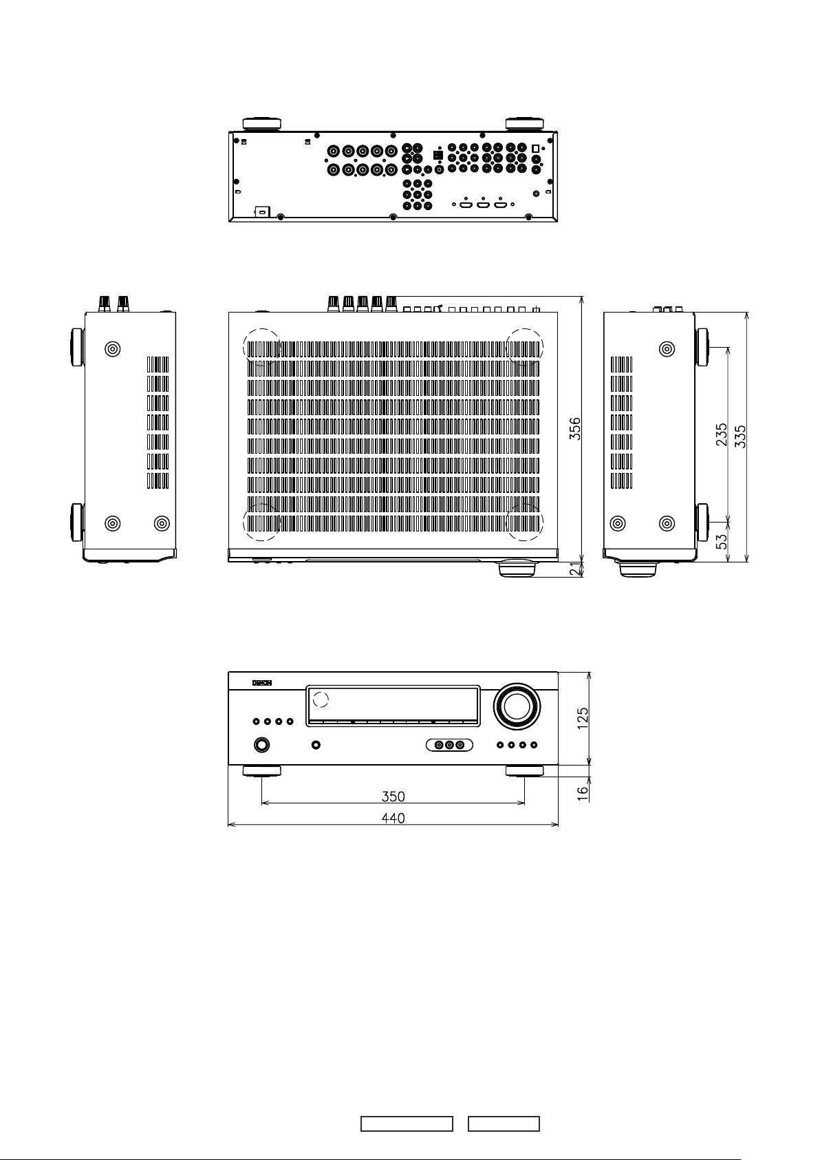
DIMENSION
AVR-390
3
DHT-390XP
AVR-390
Page 4
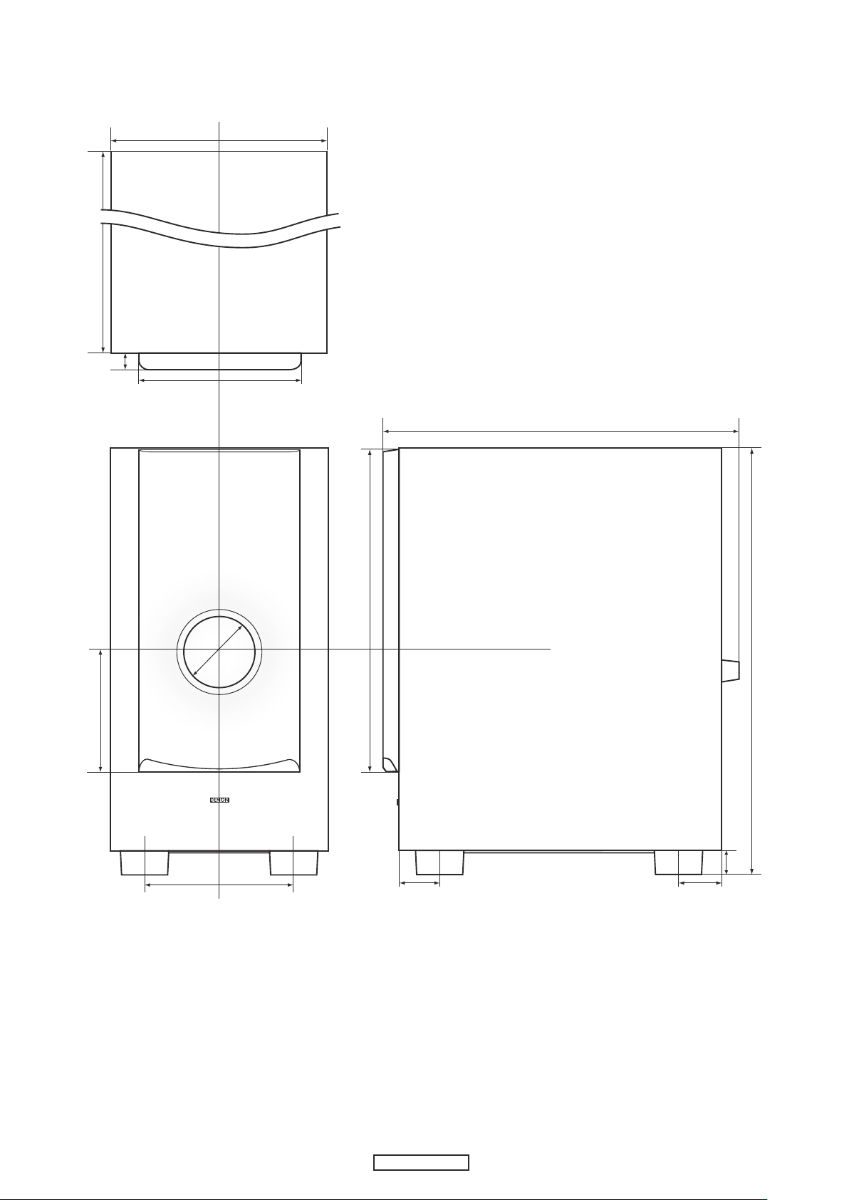
DSW-390
270
427
395
20
200
530
30
185
150
55
50
400
φ88
4
DHT-390XP
Page 5
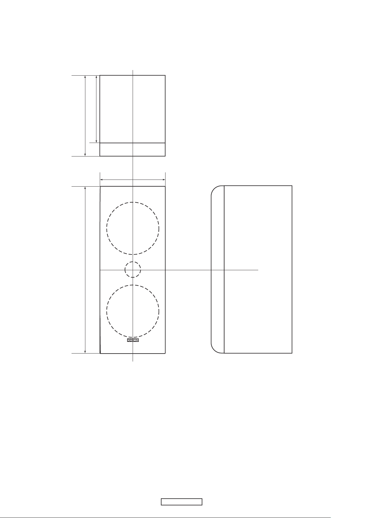
SC-F390
125
130
155
320
5
DHT-390XP
Page 6
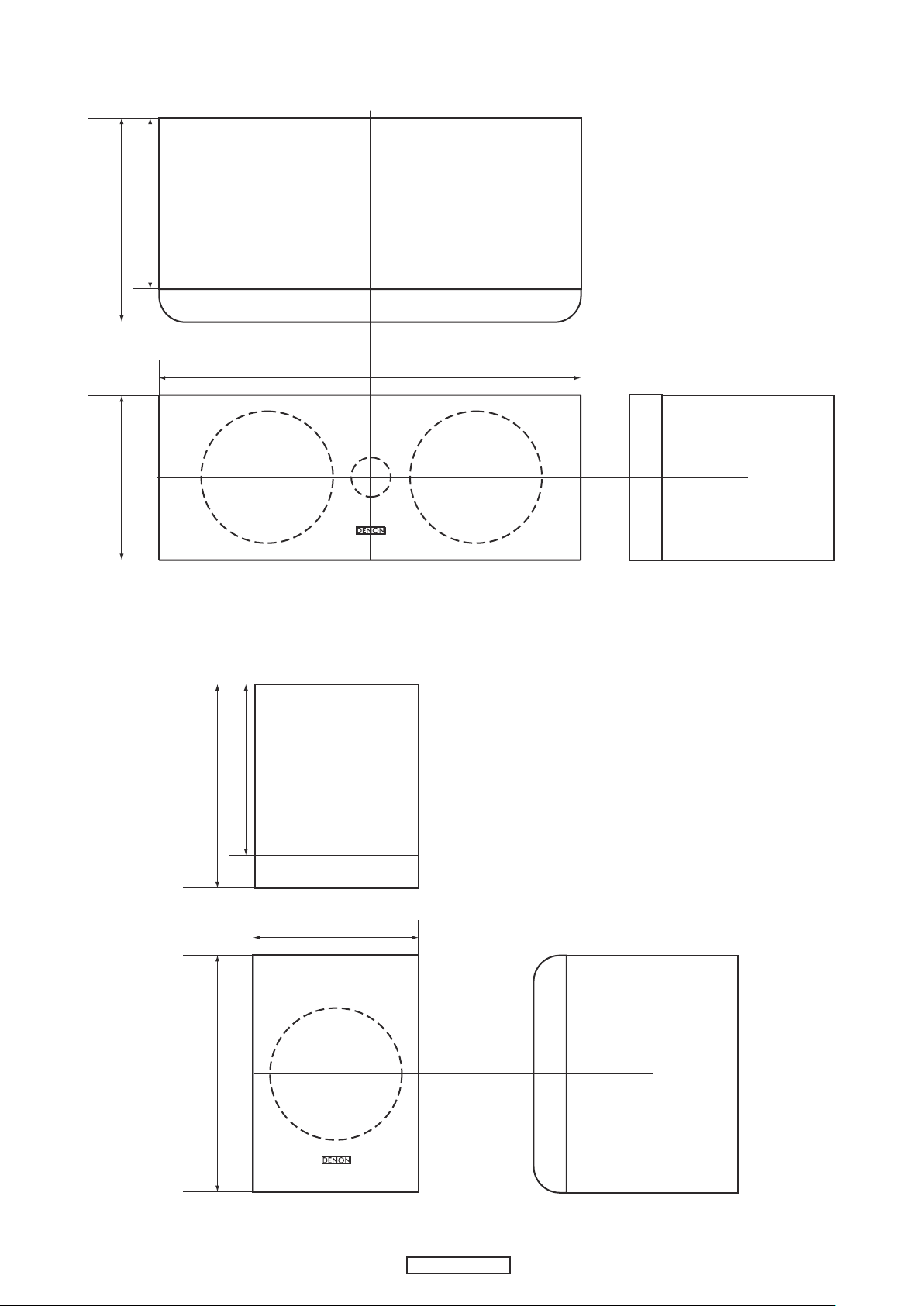
SC-C390
155
125
130
320
155
180
130
125
SC-R390
6
DHT-390XP
Page 7

WIRE ARRANGEMENT
If wire bundles are untied or moved to perform adjustment or parts replacement etc., be sure to rearrange them neatly
asthey were originally bundled or placed afterward.
Otherwise, incorrect arrangement can be a cause of noisegeneration.
Wire arrangement viewed from the top
Back Panel side
Front Panel side
7
DHT-390XP
AVR-390
Page 8

DISASSEMBLY
Y
K
Y
P
O
R
• Disassemble in order of the arrow of the figure of following flow.
• In the case of the re-assembling, assemble it in order of the reverse of the following flow.
• In the case of the re-assembling, observe "attention of assembling" it.
CABINET TOP
Refer to "DISASSEMBLY 1.PANEL FRONT ASSY" Refer to "DISASSEMBLY 5.CHASSIS BACK" Refer to "DISASSEMBLY 2.HEATSINK
PANEL FRONT ASS
and "EXPLODED VIEW" and "EXPLODED VIEW" MAIN ASSY" and "EXPLODED VIEW"
PCB ASSY ST-BY PCB ASSY AMP
(Ref. No. of EXPLODED VIEW : 11) (Ref. No. of EXPLODED VIEW : 20)
PCB ASSY TACT-SW
(Ref. No. of EXPLODED VIEW : 12)
PCB ASSY FRONT
(Ref. No. of EXPLODED VIEW : 13) Refer to "DISASSEMBLY 6.PCB ASSY DSP" Refer to "DISASSEMBLY 3.PCB ASSY HDMI"
PCB ASSY H/P and "EXPLODED VIEW" and "EXPLODED VIEW"
(Ref. No. of EXPLODED VIEW : 14) PCB ASSY DSP PCB ASSY HDMI
PCB ASSY ENCORDER (Ref. No. of EXPLODED VIEW : 32) (Ref. No. of EXPLODED VIEW : 33)
(Ref. No. of EXPLODED VIEW : 17)
Refer to "DISASSEMBLY 7.PCB ASSY VIDEO" Refer to "DISASSEMBLY 4.POWER TRANS"
PCB ASSY VIDEO POWER TRANS
(Ref. No. of EXPLODED VIEW : 31) (Ref. No. of EXPLODED VIEW : 28)
Refer to "DISASSEMBLY 8.PCB ASSY POWER"
PCB ASSY POWER
(Ref. No. of EXPLODED VIEW : 29)
Refer to "DISASSEMBLY 9.PCB ASSY MAIN"
PCB ASSY MAIN
(Ref. No. of EXPLODED VIEW : 30)
CHASSIS BAC
PCB ASSY DS
PCB ASSY VIDE
and "EXPLODED VIEW" and "EXPLODED VIEW"
PCB ASSY POWE
and "EXPLODED VIEW"
PCB ASSY MAIN
and "EXPLODED VIEW"
HEATSINK MAIN ASS
PCB ASSY HDMI
POWER TRANS
The viewpoint of each photograph
(photography direction)
[ Top view ]
Picture D
Picture E
Picture F
Picture B
( Bottom view )
Picture A
Picture C
Picture G
8
DHT-390XP
AVR-390
Page 9

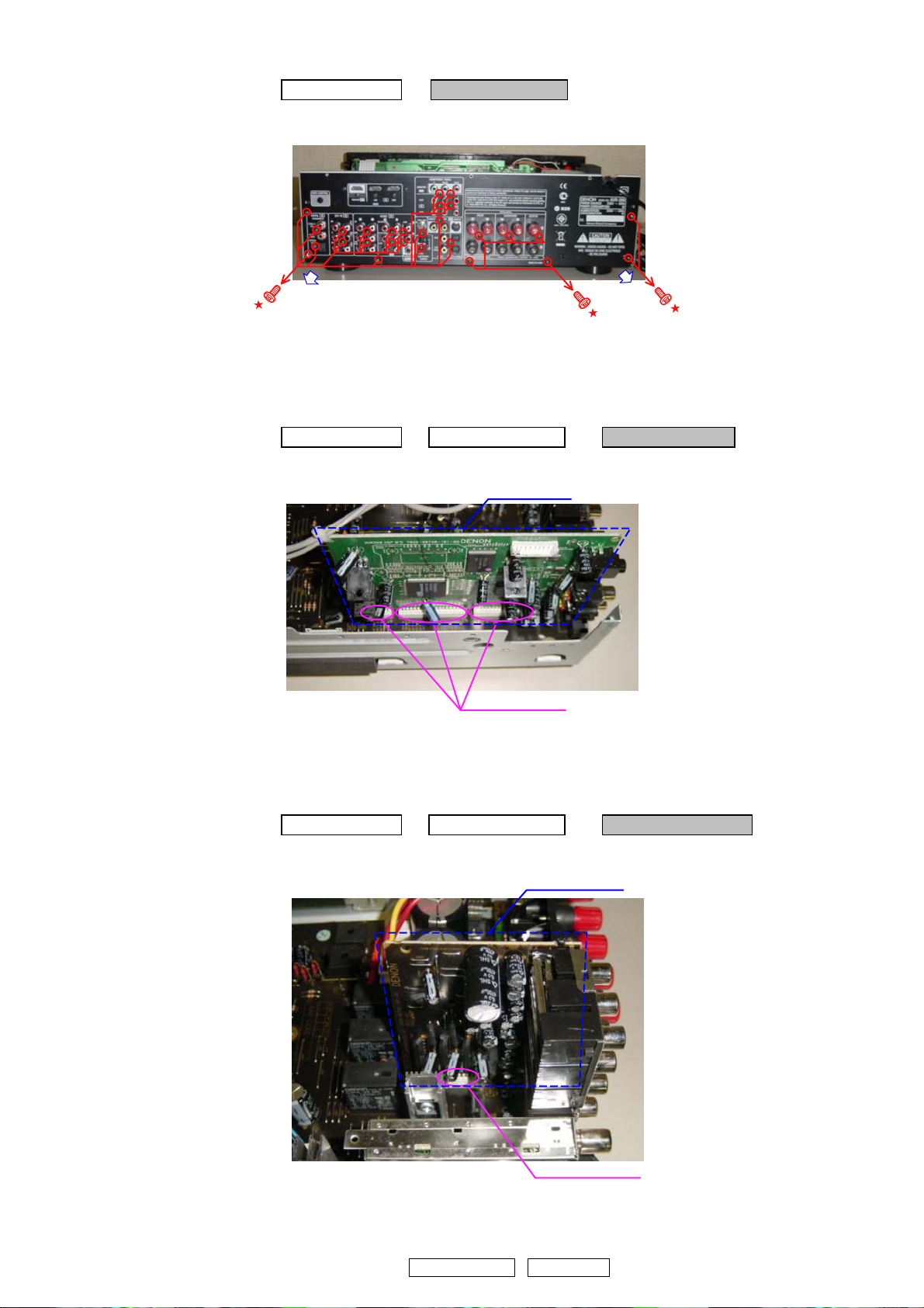
1. PANEL FRONT ASSY
Proceeding : CABINET TOP → PANEL FRONT ASSY
(1) Disconnect the connector wires and FFC Cable.
Cord holder : Loose
CP701
Top view
Picture D
(2) Remove the screws.
FFC Cable
Cord holder : Loose
CP701
CP104
cut
Bottom view
9
DHT-390XP
AVR-390
Page 10
Picture C
Picture D
Please refer to "EXPLODED VIEW" for the disassembly method of each P.W.B included in PANEL FRONT ASSY.
2. HEATSINK MAIN ASSY
Proceeding : CABINET TOP → HEATSINK MAIN ASSY
(1) Disconnect the connector wires and FFC Cable.
Cord holder : Loose
Cord holder : Loose
Top view
FFC Cable
CP110 CP 111
CP701
CP107
10
DHT-390XP
AVR-390
Page 11
(2) Remove the screws.
Bottom view
Picture C
Cord holder : Loose
Cord holder : Loose
Picture D
Please refer to "EXPLODED VIEW" for the disassembly method of each P.W.B included in HEATSINK MAIN ASSY.
11
DHT-390XP
AVR-390
Page 12
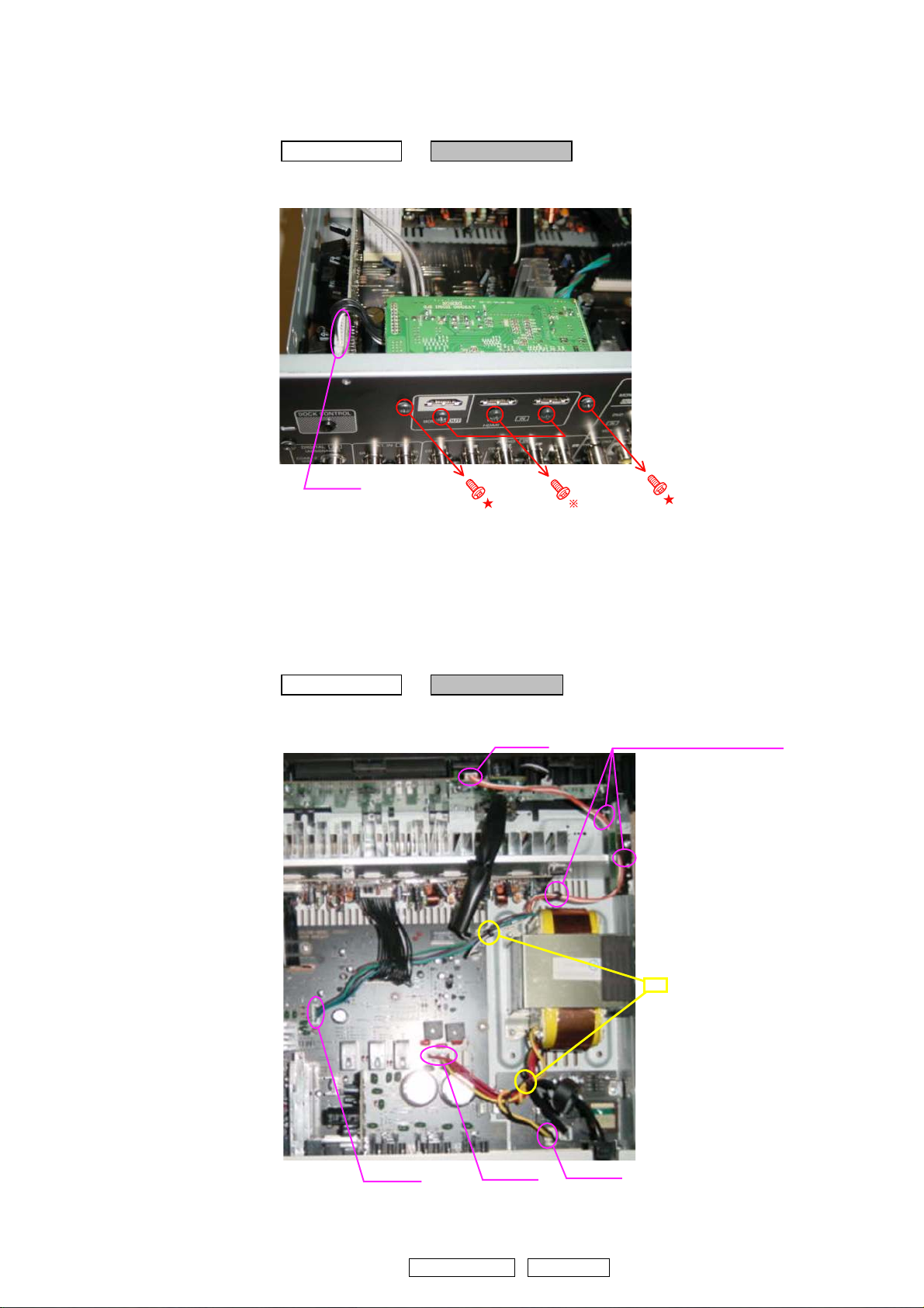
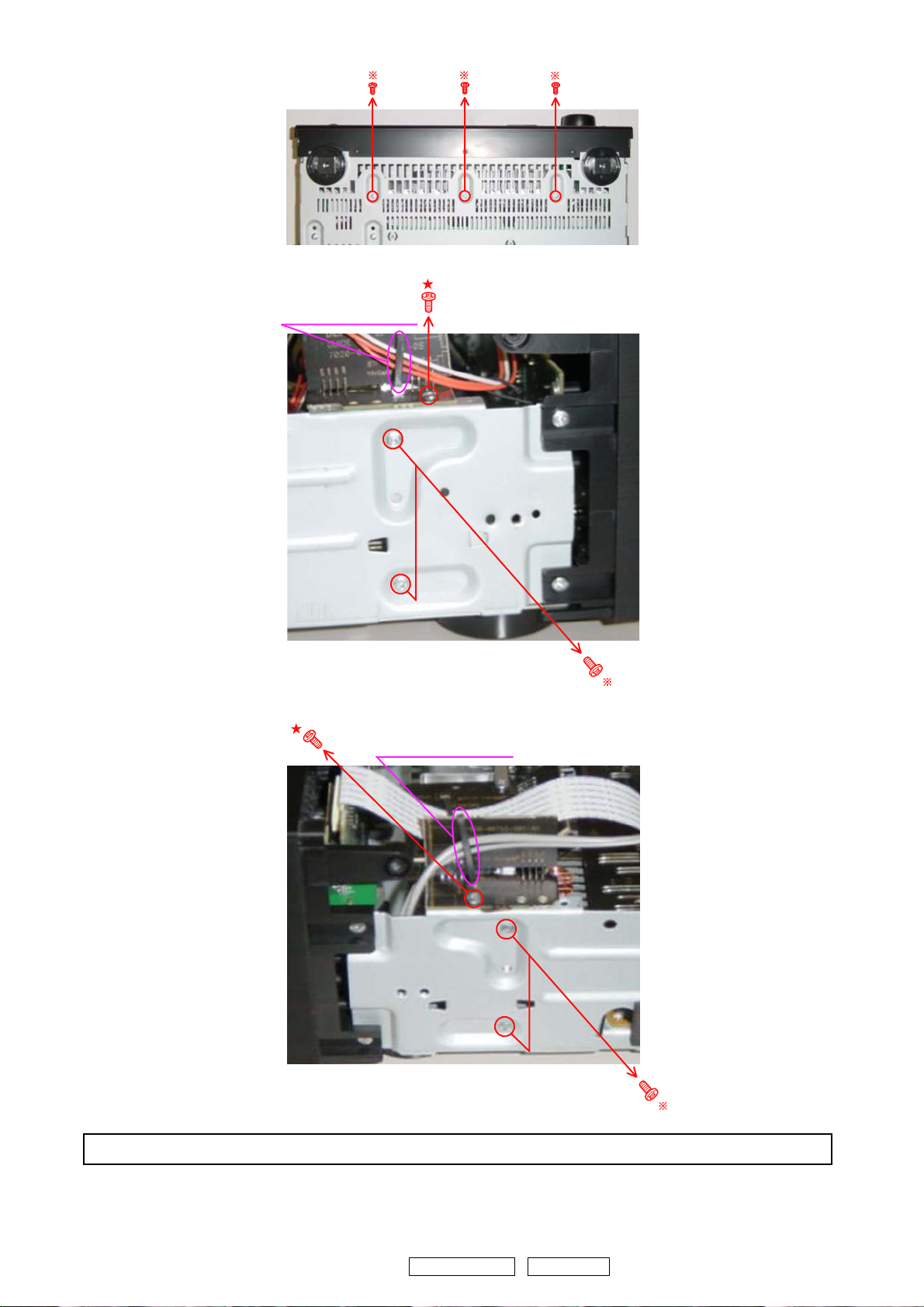
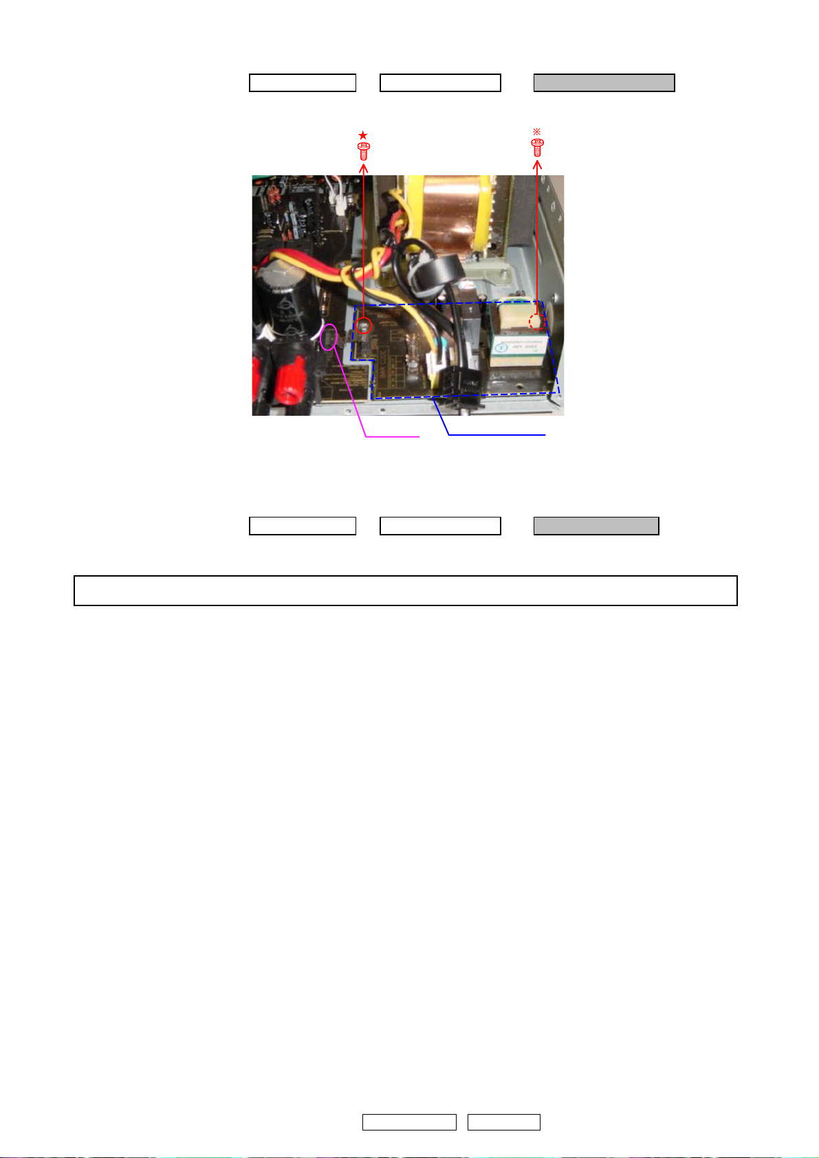
3. PCB ASSY HDMI
Proceeding : CABINET TOP → PCB ASSY HDMI
(1) Disconnect the connector wire and remove the screws.
Picture F
CP01
4. POWER TRANS
Proceeding : CABINET TOP → POWER TRANS
(1) Disconnect the connector wires.
CP701
Top view
CORD HOLDER : Loose
cut
CP102
CP101
12
DHT-390XP
CP305
AVR-390
Page 13
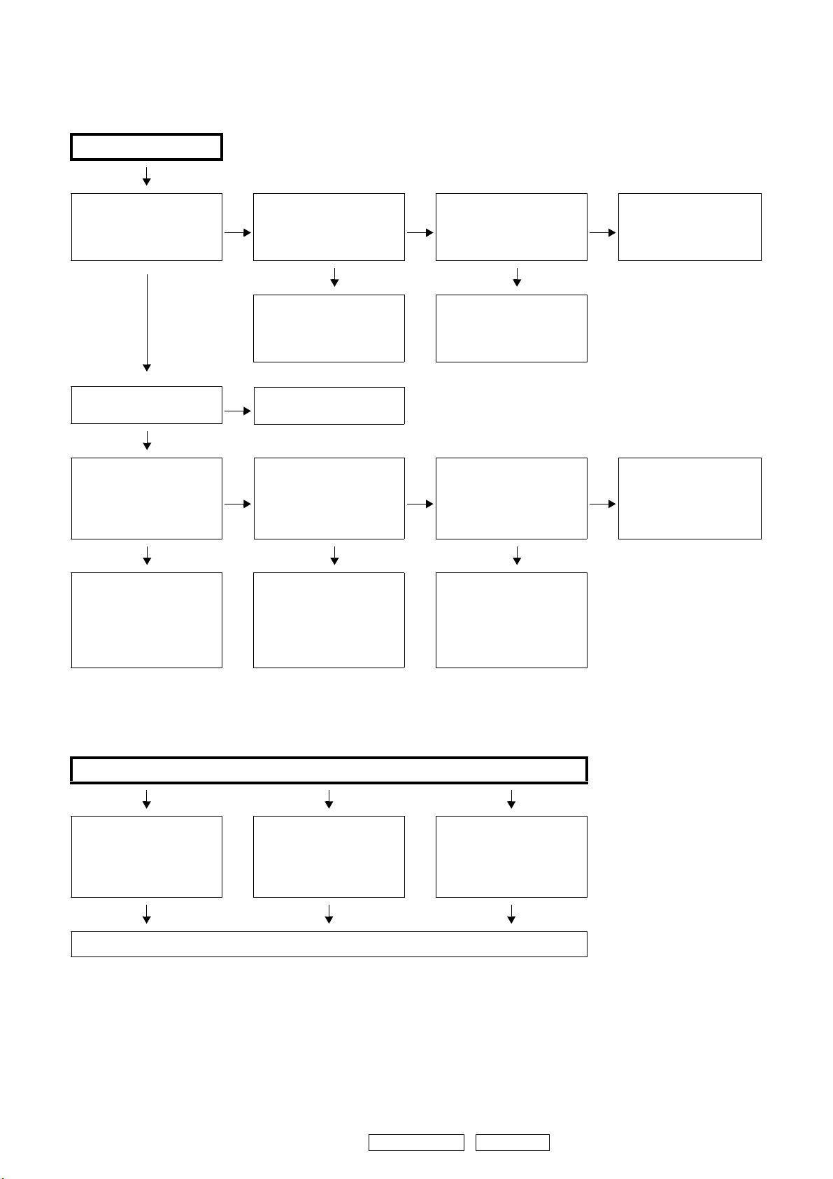
5. CHASSIS BACK
Proceeding : CABINET TOP → CHASSIS BACK
(1) Remove the screws.
Picture A
6. PCB ASSY DSP
Proceeding : CABINET TOP → CHASSIS BACK → PCB ASSY DSP
(1) Disconnect the Board to board.
DSP Board
Top view
Board to board
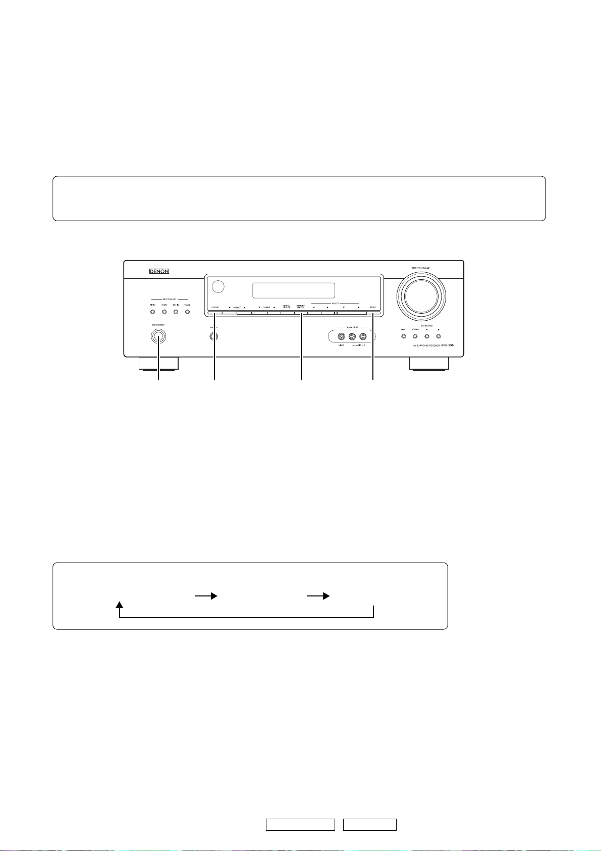
7. PCB ASSY VIDEO
Proceeding : CABINET TOP → CHASSIS BACK → PCB ASSY VIDEO
(1) Disconnect the Board to board.
VIDEO Board
Top view
13
DHT-390XP
Board to board
AVR-390
Page 14
8. PCB ASSY POWER
Proceeding : CABINET TOP → CHASSIS BACK → PCB ASSY POWER
(1) Disconnect the connector wires and remove the screws.
Top view
CP103
POWER Board
9. PCB ASSY MAIN
Proceeding : CABINET TOP → CHASSIS BACK → PCB ASSY MAIN
Please refer to "EXPLODED VIEW" for the disassembly method of PCB ASSY MAIN.
14
DHT-390XP
AVR-390
Page 15
CAUTION IN SERVICING
1. Initializing
Initialization should be performed when the µcom, peripheral parts of µcom, MAIN P.W.B. unit and Mecha are replaced.
1. Plug the power cord into a power outlet.
2. "ON/STANDBY LED" is red lighting.
3. Press the “ON/STANDBY” button while pressing the “MEMORY/ENTER” button.
4. "CLEAR" is displayed on the FL tube.
*The microprocessor will be initialized.
Note:If step 4 does not work, start over from step 1.
All user settings will be lost and this factory setting will be recovered when this initialization mode.
So make sure to m+emorize your setting for restoring after the initialization.
ON/STANDBY STATUS MEMORY/ENTER SETUP
2. Version display
1. Plug the power cord into a power outlet.
2. "ON/STANDBY LED" is red lighting.
3. Press the “ON/STANDBY” button while pressing the “SETUP” button.
4. The version of Main com is displayed on FL tube.
Version of Main com : “M:XXXX-X”
5. Press the "STATUS" or “SETUP” button, version of DSP is displayed on the FL tube.
Version of DSP : “DSP:XXXX”
6. Press the "STATUS" or “SETUP” button, the FL tube lights all.
The display switches each time the "STATUS" or “SETUP” button is pressed.
Version of Main com Version of DSP FL tube lights all
15
DHT-390XP
AVR-390
Page 16

ADJUSTMENT
VR213FR
VR213SL
VR213FL
VR213C
VR213SR
S Lch
F Lch
TP201FL
TP201SL
TP201FR
TP201C TP201SR
C ch
F Rch
S Rch
DC Voltmeter
MAIN UNIT
AMP. UNIT
Audio Section
Idling Current
Required measurement equipment: DC Voltmeter
1. Preparation
(1) Avoid direct blow from an air conditioner or an electric fan, and adjust the unit at normal room temperature 15 ˚C ~
30 ˚C (59 ˚F ~ 86 ˚F).
(2) Presetting
• POWER (Power source switch) OFF
• SPEAKER (Speaker terminal) No load
(Do not connect speaker, dummy resistor, etc.)
2. Adjustment
(1) Remove top cover and set VR213FL, FR, C, SL, SR, on Main Amp. Unit at fully counterclockwise (c) position.
(2) Connect DC Voltmeter to test points (FRONT-Lch: TP201FL, FRONT-Rch: TP201FR, CENTER ch: TP201C,
SURROUND-Lch: TP201SL, SURROUND-Rch: TP201SR).
(3) Connect power cord to AC Line, and turn power switch "ON".
(4) Presetting.
MASTER VOLUME : "---" counterclockwise (c min.)
SPEAKER (Speaker terminal) : No load
(Do not connect speaker, dummy resistor, etc.)
FUNCTION : EXT IN
(5) Within 2 minutes after the power on, turn VR101 clockwise (x) to adjust the TEST POINT voltage to
1.5 mV ± 0.5 mV DC.
(6) After 10 minutes from the preset above, turn VR101 to set the voltage to
2.0 mV ± 0.5 mV DC.
(7) Adjust the Variable Resistors of other channels in the same way.
16
DHT-390XP
AVR-390
Page 17
TROUBLE SHOOTING
1. POWER
1.1. Power not turn on
Power not turn on
Is the ON/STANDBY indica-
tor on the front panel flashing
red?
NO
Is the fuse blown?
YES
Does the power turn on when
the POWER switch is turned
off then back on?
YES YES YES
Check the primary circuitry
parts including the POWER
switch (for poor contacts,
etc.), and replace any defective parts.
Are there any incomplete
connections in the connec-
YES
tors connecting between the
various circuit boards?
Connect the connectors
properly.
NO
Refer to Fuse is blown
Is a DC 3.3V voltage being
supplied from the POWER
NO
B’d (CP103 pins 3) to the
microprocessor?
Check the microprocessor
periphery circuitry and
replace any defective parts.
Is there a short circuit
NO
between the speaker terminals and the ground?
YES NO
Check for damage in the
power amplifier circuitry parts
and replace any defective
parts.
Is a DC 3.3V voltage output
when the cord supplying the
NO
power from the SUPPLY B’d
to the microprocessor
(CP103) is unplugged?
Check the circuitry and parts
from CP103 on the SUPPLY
B’d to the microprocessor for
damage and short-circuits,
and replace any defective
parts.
Correct the short circuit
YES
between the speaker and
the ground.
Check the parts from IC300
NO
to the primary circuitry and
replace any defective parts.
1.2. Fuse is blown
Check for leaks or short circuits in the primary side
parts, and replace any
defective parts.
Fuse is blown
Check for short circuits in
the rectifier diodes and circuitry of the secondary side
rectifying circuits, and
replace any defective parts.
After repairing, also replace the fuse.
17
DHT-390XP
Check for short circuits in
the power stabilizer unit's
regulator output terminal
and the ground, and replace
any defective parts.
AVR-390
Page 18

2. Analog video
2.1. AVR-390
MONITOR OUT (CVBS/S) Output NG
Input
CVBS
A
Input
S
When checking operation, select
DVD for the function.
A
Input
CVBS/S
Check 12V, 9V.
12V : CN201-4pin
9V : CN201-6pin
To troubleshooting 1.1 Power not turn
NG
on.
OK
Check output
Output V : C258 +side
Output Y : C259 +side
Output C : C262 +side
OK
Check cable between main unit
and monitor or Check monitor.
NG
Unless specified, VIDEO UNIT part.
Check input of input selector and
surrounding circuitry soldering.
Input : IC202,IC203,IC204
18
DHT-390XP
AVR-390
Page 19

3. HDMI/DVI
3.1. No picture or sound is output
No picture or sound is output
YES
Check the HDMI/DVI cable
connection
YES
Is the HDMI/DVI cable properly
connected?
YES
Are you using an HDMI/DVI selector,
repeater or a device for improving
picture quality?
NO
Are you using a certified HDMI cable
(one with the HDMI stamp)?
YES
Are you using an HDMI/DVI cable less
than 5 meters in length?
YES
Are the picture and sound output when
another HDMI/DVI cable is used?
NO
Checking the DVD player
There may be a problem with the HDMI/
NO
DVI cable. Check the connection.
Disconnect everything and connect only
YES
the HDMI/DVI cable to check.
Use a certified HDMI cable (one with the
NO
HDMI stamp).
Replace the HDMI/DVI cable with one
NO
that is less than 5 meters in length (2
meters recommended) to check.
YES
The HDMI/DVI cable is defective.
YES
Is the DVD player's HDMI output setting
correct?
YES
Are the picture and sound TV output
when the DVD player's resolution is
changed?
NO
Is the DVD player HDCP-compatible?
NO
Are the picture and sound output when
a different DVD player is used?
NO
Check the HDMI output setting, referring
YES
to the DVD player's operating
instructions.
Set the DVD player's output resolution
YES
to a resolution with which the TV is
compatible.
The DVD player may not be compatible
YES
with HDCP TV. Ask the DVD player's
manufacturer.
YES
The DVD player is defective.
19
DHT-390XP
AVR-390
Page 20
Check the TV
Is the TV HDCP-compatible?
Is the TV compatible with resolutions of 1080P?
Is the TV's input set to HDMI?
YES
YES
YES
Use an HDCP-compatible TV. PC
NO
TVs cannot be used.
If the TV is not compatible with
resolutions of 1080P, no picture will
NO
be output, even if the DVD player's
resolution is set to 1080P.
Check the TV's input setting,
NO
referring to the TV's operating
instructions.
Are the picture and sound output when a different TV is used?
YES
Check the set (AVR-390)
Is the set's input set to HDMI?
YES YES
The set does not recognize the TV.
Is IC01 pin 76 "H" (3V-5V)? With the TV
connected, check the voltage of the IC
on the side on which the TV is
connected.
YES
When using a DENON DVD player, is
the fluorescent display tube's "HDMI"
indicator lit?
If using a non-DENON DVD player,
proceed to "NO".
The pattern and circuit from the HDMI
NO
connector (JACK03) to the IC (IC01)
is defective.
The DVD player does not recognize
the connection with the set.
Is the HDMI connector (JACK01/
NO
JACK02) pin 19 "H" (5V)? With the DVD
player connected, check the voltage of
the HDMI connector for the input on the
side on which the DVD player is
connected.
NO
The TV is defective.
Check the set's input setting,
NO
referring to the set's operating
instructions.
The pattern and circuit from the
HDMI connector (JACK01/
NO
JACK02) to the Main com is
defective.
YES YES
The HDMI output circuitry is defective.
(IC01 and surrounding circuitry)
20
DHT-390XP
AVR-390
Page 21
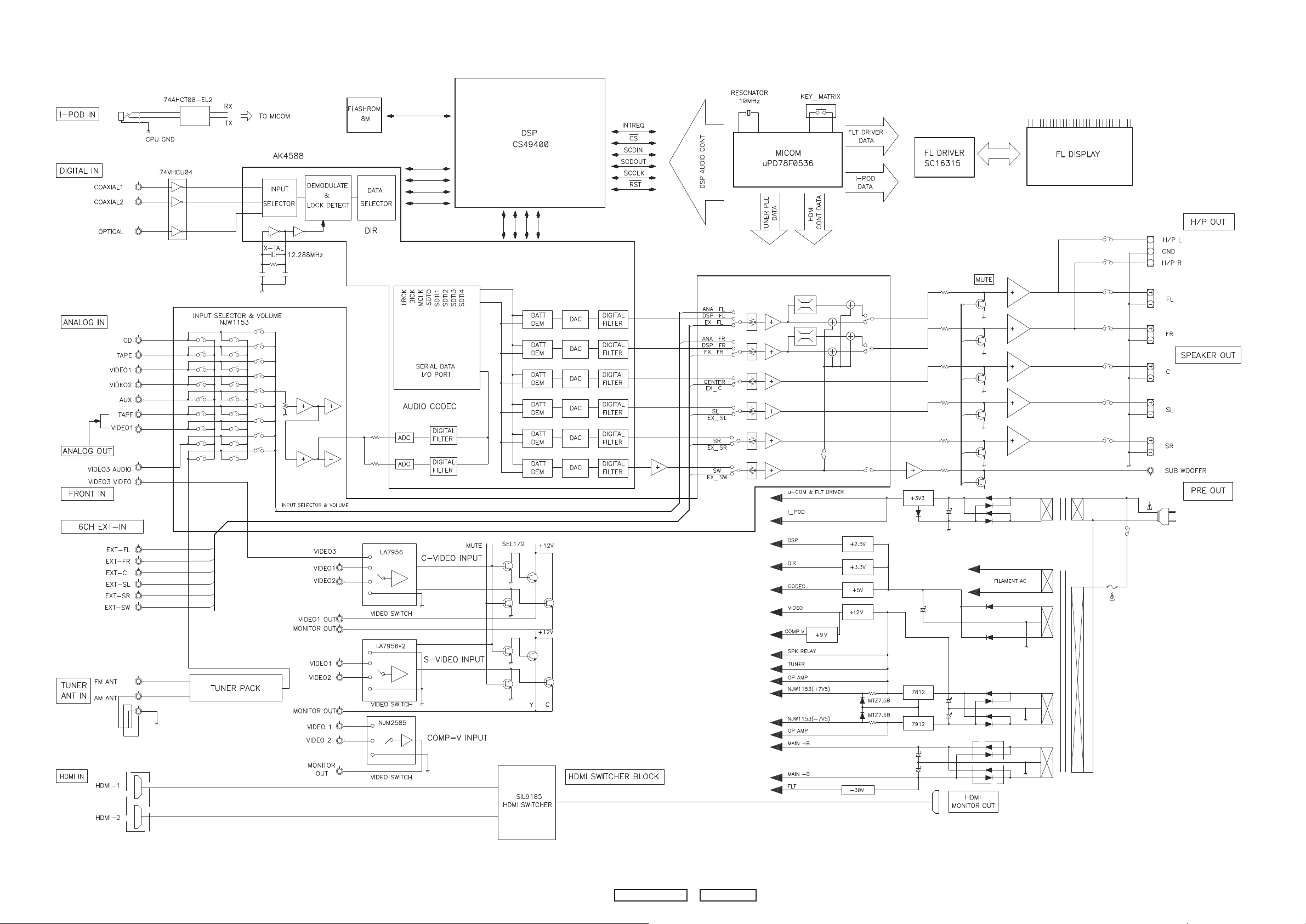
BLOCK DIAGRAMS
AVR-390 AUDIO BLOCK DIAGRAM
21
DHT-390XP
AVR-390
Page 22
AVR-390 GND BLOCK DIAGRAM
22
DHT-390XP
AVR-390
Page 23
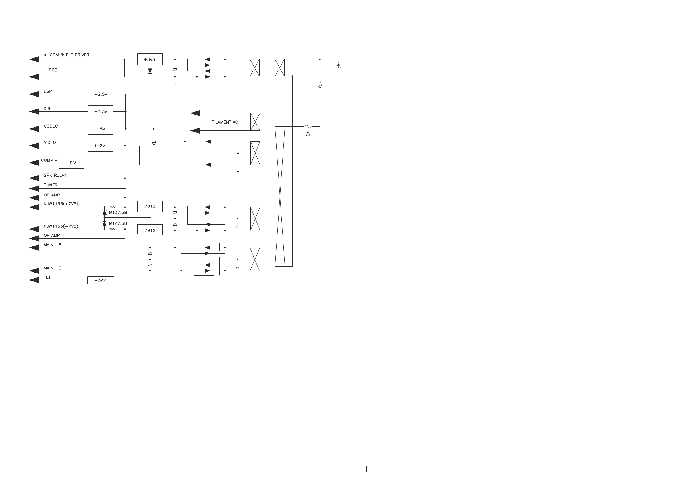
AVR-390 VCC BLOCK DIAGRAM
23
DHT-390XP
AVR-390
Page 24
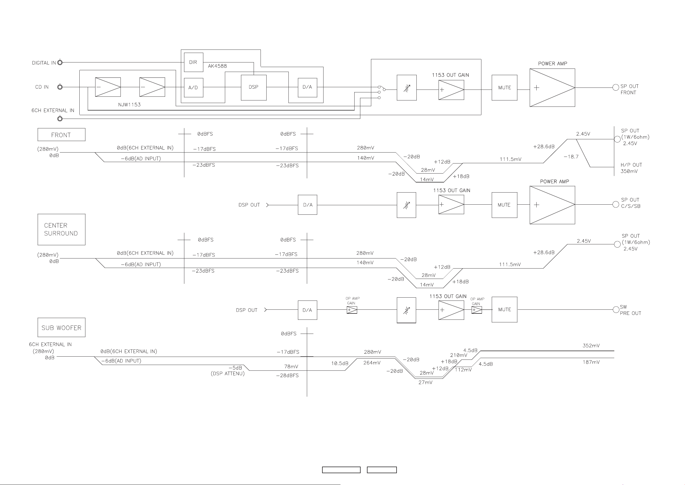
LEVEL DIAGRAM
AVR-390
24
DHT-390XP
AVR-390
Page 25
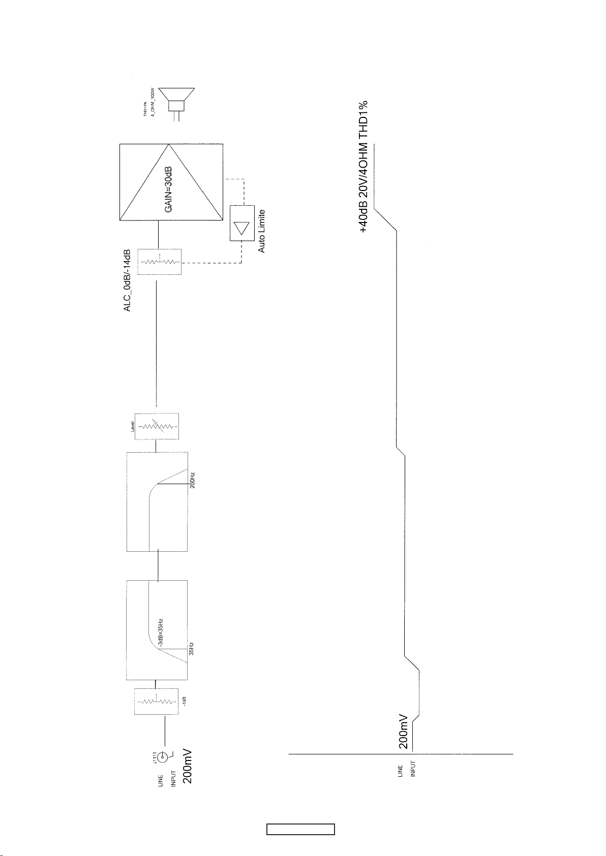
BLOCK / LEVEL DIAGRAM
DSW-390
25
DHT-390XP
Page 26

SEMICONDUCTORS
FILT1
FILT2
CLKIN, XTALI
XTALO
CLKSEL
7TADF
6TADF
5TADF
4TADF
3TADF
2TADF
ADF T1
0TADF
KLCCSF,OAF
NIDCSF,1AF
,1SHF DRF /RF, W
,0SHF RWF , SDF
SCF
TUODCSF,OIDCSF,2SHF
QERTNIF
FSCLKN1, STCCLK2
FLRCLKN1
FSDATAN1
CMPCLK, FSCLKN2
CMPDAT, FSDATAN2
KCBDF
ADBDF
PLLVDD
PLLVSS
RESET
TSET
KLCM
0KLCS
1KLCS
0KLCRL
1KLCRL
AUDATA0
AUDATA1
2ATADUA
A859TMX,3ATADUA
TADUA 82OIPG,4A
92OIPG,5ATADUA
03OIPG,6ATADUA
13OIPG,B859TMX,7ATADUA
KCBD
ADBD
22OIPG,NKLCS
32OIPG,NKLCRL
TADS 42OIPG,0NA
52OIPG,1NATADS
OIPG,2NATADS 26
OIPG,3NATADS 27
SCS
SCCLK
SCDIN
SCDOUT, SCDIO
QERTNI , TOOBA
7OIPG,7ATADH
6OIPG,6ATADH
5OIPG,5ATADH
4OIPG,4ATADH
3OIPG,3ATADH
HDATA2, GPIO2
HDATA1, GPIO1
HDATA0, GPIO0
A0, GPIO13
A1, GPIO12
SD_ADDR8, EXTA8
SD_ADDR7, EXTA7
SD_ADDR6, EXTA6
SD_ADDR5, EXTA5
SD_ADDR4, EXTA4
TXE,3RDDA_DS 3A
2ATXE,2RDDA_DS
1ATXE,1RDDA_DS
0ATXE,0RDDA_DS
SD_CLK_OUT
SD_CLK_IN
SD_DATA8, EXTA11
SD_DATA7, EXTD7
SD_DATA6, EXTD6
SD_DATA5, EXTD5
SD_DATA4, EXTD4
SD_DATA3, EXTD3
2DTXE,2ATAD_DS
1DTXE,1ATAD_DS
0DTXE,0ATAD_DS
SD_ADDR10, EXTA10
SD_ADDR9, EXTA9
RD, R/W, GPIO11
WR, DS, GPIO10
CS, GPIO9
HINBSY, GPIO8
SD_DATA15, EXTA18
SD_DATA14, EXTA17
SD_DATA13, EXTA16
SD_DATA12, EXTA15
SD_DATA11, EXTA14
SD_DATA10, EXTA13
SD_DATA9, EXTA12
UHS2, CS_OUT, GPIO17
81OIPG,0SHU
91OIPG,1SHU
02OIPG
12OIPG
VDD4
7DDV
1DDV
VDD3
VSS4
SSV 7
1SSV
VSS3
6DDV
2DDV
VDD5
6SSV
2SSV
VSS5
VDDSD1
VDDSD2
VDDSD3
SD_CLK_EN
SD_BA, EXTA19
SD_CS
SAR_DS
SAC_DS
EW_DS
SD_DQM1
SD_DQM0
SC_VN 41OIPG,
EO_VN 51OIPG,
W_VN E 61OIPG,
VDDSD4
VSSSD1
VSSSD2
VSSSD3
VSSSD4
1CN
2CN
3CN
4CN
NC5
CMPREQ, FLRCLKN2
1
5
01
15
20
25
30
40
45
50
55
60
65
70
75
08
85
90
59
100
501
115
110
120
125
130
135
140
144
35
Only major semiconductors are shown, general semiconductors etc. are omitted to list.
The semiconductor which described a detailed drawing in a schematic diagram are omitted to list.
1. IC's
CS494003-CQZ (IC403)
26
DHT-390XP AVR-390
Page 27

PIN FUNCTION
PIN NAME FUNCTION
FILT1 Phase-Locked Loop Filter
FILT2 Phase Locked Loop Filter
CLKIN, XTALI External Clock Input/Crystal Oscillator Input
XTALO Crystal Oscillator Output
CLKSEL DSP Clock Select
FDAT6, FDAT7
FDAT4, FDAT5
FDAT2, FDAT3
FDAT0, FDAT1
FA0, FSCCLK Host Parallel Address Bit Zero or Serial Control Port Clock
FA1, FSCDIN Host Address Bit One or SPI Serial Control Data Input
FHS1, FRD
FHS0, FWR, FDS Mode Select Bit 0 or Host Write Strobe or Host Data Strobe
FCS Host Parallel Chip Select, Host Serial SPI Chip Select
FHS2, FSCDIO, FSCDOUT Mode Select Bit 2 or Serial Control Port Data Input and Output, Parallel Port Type Select
FINTREQ Control Port Interrupt Request
FSCLKN1, STCCLK2 PCM Audio Input Bit Clock
FLRCLKN1 PCM Audio Input Sample Rate Clock
FSDATAN1 PCM Audio Data Input One
CMPCLK, FSCLKN2 PCM Audio Input Bit Clock
CMPDAT, FSDATAN2 PCM Audio Data Input Number Two
FDBCK Reserved
FDBDA Reserved
PLLVDD PLL Supply Voltage
PLLVSS PLL Ground Voltage
RESET Master Reset Input
TEST Reserved
MCLK Audio Master Clock
SCLK0 Audio Output Bit Clock
SCLK1 Audio Output Bit Clock
LRCLK0 Audio Output Sample Rate Clock
LRCLK1 Audio Output Sample Rate Clock
AUDATA0 Digital Audio Output 0
AUDATA1 Digital Audio Output 1
AUDATA2 Digital Audio Output 2
AUDATA3, XMT958A Digital Audio Output 3, S/PDIF Transmitter
AUDATA4, GPIO28 Digital Audio Output 4, General Purpose I/O
AUDATA5, GPIO29 Digital Audio Output 5, General Purpose I/O
AUDATA6, GPIO30 Digital Audio Output 6, General Purpose I/O
AUDATA7, XMT958B, GPIO31 Digital Audio Output 7, S/PDIF Transmitter, General Purpose I/O
DBCK Debug Clock
DBDA Debug Data
SLCKN, GPIO22 PCM Audio Input Bit Clock, General Purpose I/O
LRCLKN, GPIO23 PCM Audio Input Sample Rate Clock, General Purpose I/O
SDATAN0, GPIO24 PCM Audio Input Data, General Purpose I/O
SDATAN1, GPIO25 PCM Audio Input Data, General Purpose I/O
SDATAN2, GPIO26 PCM Audio Input Data, General Purpose I/O
SDATAN3, GPIO27 PCM Audio Input Data, General Purpose I/O
SCS Host Serial SPI Chip Select
SCCLK Serial Control Port Clock
SCDIN SPI Serial Control Data Input
SCDOUT, SCDIO Serial Control Port Data Input and Output
INTREQ Control Port Interrupt Request
HDATA7, GPIO7
HDATA6, GPIO6
HDATA5, GPIO5
HDATA4, GPIO4
HDATA3, GPIO3
HDATA2, GPIO2
HDATA1, GPIO1
HDATA0, GPIO0
A0, GPIO13 Host Parallel Address Bit 0, General Purpose I/O
A1, GPIO12 Host Address Bit 1, General Purpose I/O
RD, R/W, GPIO11 Host Parallel Output Enable, Host Parallel R/W, General Purpose I/O
WR, DS, GPIO10 Host Write Strobe, Host Data Strobe, General Purpose I/O
CS, GPIO9 Host Parallel Chip Select, General Purpose I/O
, FR/W Mode Select Bit 1 or Host Parallel Output Enable or Host Parallel R/W
DSPAB Bidirectional Data Bus
DSPC Bidirectional Data Bus, General Purpose I/O
27
DHT-390XP AVR-390
Page 28

PIN NAME FUNCTION
HINBSY, GPIO8 Input Host Message Status, General Purpose I/O
SD_DATA15, EXTA18
SD_DATA14, EXTA17
SD_DATA13, EXTA16
SD_DATA12, EXTA15
SD_DATA11, EXTA14
SD_DATA10, EXTA13
SD_DATA9, EXTA12
SD_DATA8, EXTA11
SD_DATA7, EXTD7
SD_DATA6, EXTD6
SD_DATA5, EXTD5
SD_DATA4, EXTD4
SD_DATA3, EXTD3
SD_DATA2, EXTD2
SD_DATA1, EXTD1
SD_DATA0, EXTD0
SD_ADDR10, EXTA10
SD_ADDR9, EXTA9
SD_ADDR8, EXTA8
SD_ADDR7, EXTA7
SD_ADDR6, EXTA6
SD_ADDR5, EXTA5
SD_ADDR4, EXTA4
SD_ADDR3, EXTA3
SD_ADDR2, EXTA2
SD_ADDR1, EXTA1
SD_ADDR0, EXTA0
SD_CLK_OUT SDRAM Clock Output
SD_CLK_IN SDRAM Re-timing Clock Input
SD_CLK_EN SDRAM Clock Enable
SD_BA, EXTA19 SDRAM Bank Address Select, SRAM External Address Bus
SD_CS SDRAM Chip Select
SD_RAS SDRAM Row Address Strobe
SD_CAS SDRAM Column Address Strobe
SD_WE SDRAM Write Enable
SD_DQM1 SDRAM Data Mask 1
SD_DQM0 SDRAM Data Mask 2
NV_CS, GPIO14 SRAM Chip Select, General Purpose I/O
NV_OE, GPIO15 SRAM Output Enable, General Purpose I/O
NV_WE, GPIO16 SRAM Write Enable, General Purpose I/O
UHS2, CS_OUT, GPIO17 Mode Select Bit 2, External Serial Memory Chip Select, General Purpose I/O
UHS0, GPIO18 Mode Select Bit 0, General Purpose I/O
UHS1, GPIO19 Mode Select Bit 1, General Purpose I/O
GPIO20 General Purpose I/O
GPIO21 General Purpose I/O
VDD[7:1] 2.5V Supply Voltage
VSS 2.5V Ground
NC[5:1] No Connect
VDDSD[4:1] 3.3V SDRAM/SRAM/EPROM Interface Supply
VSSSD 3.3V SDRAM/SRAM/EPROM Interface Ground
SDRAM Data Bus, SRAM External Address Bus
SDRAM Data Bus, SRAM External Data Bus
SDRAM Address Bus, SRAM External Address Bus
28
DHT-390XP AVR-390
Page 29

AK4588 (IC401)
a q
(Top View)
CCLK/SC
L
CDTI/SD
A
CSN
DAUX1
SDTI4
SDTI3
SDTI2
SDTI1
XTL1
XTL0
PDN
MASTE
R
DZF2
DZF1
LOUT4
N
C
ROUT4
N
C
LOUT3
N
C
21
22
23
24
25
26
27
28
29
30
31
32
33
34
35
36
37
38
39
40
60
59
58
57
56
55
54
53
52
51
50
49
48
47
46
45
44
43
42
41
80
79
78
77
76
75
74
73
72
71
70
69
68
67
66
65
64
63
62
61
1
2
3
4
5
6
7
8
9
10
11
12
13
14
15
16
17
18
19
20
INT1
BOUT
TVDD
DVDD
DVSS
XT O
XTI
TEST3
MCKO2
MCKO1
COUT
UOUT
VOUT
SDTO2
BICK2
LRCK2
SDTO1
BICK1
LRCK1
CDTO
TEST1
RX1
NC
RX0
AVSS
AVDD
VREFH
VCOM
RIN
LIN
NC
ROUT1
NC
LOUT1
NC
ROUT2
NC
LOUT2
NC
ROUT3
INT0
TX1
TX0
MCLK
VIN
DAUX2
I2C
RX7
CAD1
RX6
CAD0
RX5
TEST2
RX4
PVDD RPVSS
RX3
NC
RX2
Input
Selector
Clock
Recovery
Clock
Generator
DAIF
Decode r
A
C-3/MPEG
Detect
DEM
PP I/F
A
udio
I/F
X'tal
Oscillator
PDN
INT0
LRCK2
BICK2
SDTO2
DAUX2
MCKO2
XTOXTI
RPVDDPVSS
CDTI
CDTO
CCLK
CSN
DVDD
DVSS
TVDD
MCKO1
I2C
RX0
RX1
RX2
RX3
RX4
RX5
RX6
RX7
DIT
TX0
Error &
Detect
STATUS
INT1
Q-subcode
buffe
r
TX1
B,C,U,
VOUT
8 to 3
VIN
Audio
I/F
LPF
LPF
LPF
LPF
LPF
LPF
LOUT1
ROUT1
LOUT2
ROUT2
LOUT3
ROUT3
DAC
DATT
DEM
ADC
HPF
ADC
HPF
RIN
LIN
LRCK1
BICK1
SDTI1
SDTI2
SDTI3
DAUX1
MCLK
LRCK
BICK
SDOUT
SDIN1
SDIN2
SDIN3
MCLK
SDTO1
Forma t
Converte r
SDTI4
SDIN4
LPF
LPF
LOUT4
ROUT4
DAC
DATT
DEM
DAC
DATT
DEM
DAC
DATT
DEM
DAC
DATT
DEM
DAC
DATT
DEM
DAC
DATT
DEM
DAC
DATT
DEM
A
VDD
A
VSS
BLOCK DIAGRAM
29
DHT-390XP AVR-390
Page 30

PIN FUNCTION
No. Pin Name I/O Function
1 INT1 O Interrupt 1 Pin
2 BOUT O
3 TVDD - Output Buffer Power Supply Pin, 2.7V~5.5V
4 DVDD - Digital Power Supply Pin, 4.5V~5.5V
5 DVSS - Digital Ground Pin
6 XTO O X'tal clock Output Pin
7 XTI I X'tal / External clock Input Pin
8 TEST3 I
9 MCKO2 O Master Clock Output 2 Pin
10 MCKO1 O Master Clock Output 1 Pin
11 COUT O C-bit Output Pin for Receiver Input
12 UOUT O U-bit Output Pin for Receiver Input
13 VOUT O V-bit Output Pin for Receiver Input
14 SDTO2 O Audio Serial Data Output Pin (DIR/DIT part)
15 BICK2 I/O Audio Serial Data Clock Pin (DIR/DIT part)
16 LRCK2 I/O Channel Clock Pin (DIR/DIT part)
17 SDTO1 O Audio Serial Data Output Pin (ADC/DAC part)
18 BICK1 I/O Audio Serial Data Clock Pin (ADC/DAC part)
19 LRCK1 I/O Input Channel Clock Pin
20 CDTO O Control Data Output Pin in Serial Mode, I2C pin= "L"
CCLK I Control Data Clock Pin in Serial Mode, I2C pin= "L"
21
SCL I Control Data Clock Pin in Serial Mode, I2C pin= "H"
CDTI I Control Data Input Pin in Serial Mode, I2C pin= "L".
22
SDA I/O Control Data Pin in Serial Mode, I2C pin= "H".
23 CSN
24 DAUX1 I AUX Audio Serial Data Input Pin (ADC/DAC part)
25 SDTI4 I DAC4 Audio Serial Data Input Pin
26 SDTI3 I DAC3 Audio Serial Data Input Pin
27 SDTI2 I DAC2 Audio Serial Data Input Pin
28 SDTI1 I DAC1 Audio Serial Data Input Pin
29 XTL1 I X'tal Frequency Select 0 Pin
30 XTL0 I X'tal Frequency Select 1 Pin
31 PDN I
32 MASTER I
DZF2 O
33
OVF O
34 DZF1 O
35 LOUT4 O DAC4 Lch Analog Output Pin
36 NC -
37 ROUT4 O DAC4 Rch Analog Output Pin
38 NC -
39 LOUT3 O DAC3 Lch Analog Output Pin
40 NC -
41 ROUT3 O DAC3 Rch Analog Output Pin
42 NC -
43 LOUT2 O DAC2 Lch Analog Output Pin
44 NC -
45 ROUT2 O DAC2 Rch Analog Output Pin
Block-Start Output Pin for Receiver Input
"H" during rst 40 ames.
Test 3 Pin
This pin should be connected to DVSS.
I Chip Select Pin in Serial Mode, I2C pin= "L".
I This pin should be connected to DVSS, I2C pin= "H".
Power-Down Mode Pin
When “L”, the AK4588 is powered-down, all output pin goes “L”, all registers are reset.
When CAD1-0 pins are changed, the AK4588 should be reset by PDN pin.
Master Mode Select Pin
“H”: Master mode, “L”: Slave mode
Zero Input Detect 2 Pin (Table 13)
When the input data of the group 1 follow total 8192 LRCK cycles with “0” input data, this pin goes to
“H”. When RSTN1 bit is “0” or PWDAN bit is “0”, this pin goes to “H”.
Analog Input Overow Detect Pin
This pin goes to “H” if the analog input of Lch or Rch overows. This pin becomes OVF pin if OVFE
bit is set to 1.
Zero Input Detect 1 Pin (Table 13)
When the input data of the group 1 follow total 8192 LRCK cycles with “0” input data, this pin goes to “H”.
When RSTN1 bit is “0” or PWDAN bit is “0”, this pin goes to “H”.
No Connect pin
No internal bonding. This pin should be opened.
No Connect pin
No internal bonding. This pin should be opened.
No Connect pin
No internal bonding. This pin should be opened.
No Connect pin
No internal bonding. This pin should be opened.
No Connect pin
No internal bonding. This pin should be opened.
30
DHT-390XP AVR-390
Page 31

No. Pin Name I/O Function
46 NC -
47 LOUT1 O DAC1 Lch Analog Output Pin
48 NC -
49 ROUT1 O DAC1 Rch Analog Output Pin
50 NC -
51 LIN I Lch Analog Input Pin
52 RIN I Rch Analog Input Pin
53 VCOM -
54 VREFH - Positive Voltage Reference Input Pin, AVDD
55 AVDD - Analog Power Supply Pin, 4.5V~5.5V
56 AVSS - Analog Ground Pin, 0V
57 RX0 I Receiver Channel 0 Pin (Internal biased pin. Internally biased at PVDD/2)
58 NC -
59 RX1 I Receiver Channel 1 Pin (Internal biased pin. Internally biased at PVDD/2)
60 TEST1 I
61 RX2 I Receiver Channel 2 Pin (Internal biased pin. Internally biased at PVDD/2)
62 NC -
63 RX3 I Receiver Channel 3 Pin (Internal biased pin. Internally biased at PVDD/2)
64 PVSS - PLL Ground pin
65 R -
66 PVDD - PLL Power supply Pin, 4.5V~5.5V
67 RX4 I Receiver Channel 4 Pin (Internal biased pin. Internally biased at PVDD/2)
68 TEST2 I
69 RX5 I Receiver Channel 5 Pin (Internal biased pin. Internally biased at PVDD/2)
70 CAD0 I Chip Address 0 Pin (ADC/DAC part)
71 RX6 I Receiver Channel 6 Pin (Internal biased pin. Internally biased at PVDD/2)
72 CAD1 I Chip Address 1 Pin (ADC/DAC part)
73 RX7 I Receiver Channel 7 Pin (Internal biased pin. Internally biased at PVDD/2)
74 I2C I
75 DAUX2 I Auxiliary Audio Data Input Pin (DIR/DIT part)
76 VIN
77 MCLK I Master Clock Input Pin
78 TX0 O Transmit Channel (Through Data) Output 0 Pin
79 TX1 O
80 INT0 O Interrupt 0 Pin
No Connect pin
No internal bonding. This pin should be opened.
No Connect pin
No internal bonding. This pin should be opened.
No Connect pin
No internal bonding. This pin should be opened.
Common Voltage Output Pin
2.2μF capacitor should be connected to AVSS externally.
No Connect pin
No internal bonding. This pin should be connected to PVSS.
Test 1 Pin
This pin should be connected to PVSS.
No Connect pin
No internal bonding. This pin should be connected to PVSS.
External Resistor Pin
12kΩ +/-1% resistor should be connected to PVSS externally.
Test 2 Pin
This pin should be connected to PVSS.
Control Mode Select Pin.
"L" : 4-wire Serial, "H" : I
I V-bit Input Pin for Transmitter Output
Transmit Channel Output1 pin
When TX bit = "0", Transmit Channel (Through Data) Output 1 Pin.
When TX bit = "1", Transmit Channel (DAUX2 Data) Output Pin (Default).
2
C Bus
Note: All input pins except internal biased pins and internal pull-down pin should not be left oating.
31
DHT-390XP AVR-390
Page 32

Sil9185 (IC01)
19
18
17
16
15
14
13
12
11
10
9
8
7
6
5
4
3
2
1
20
AGND
R0XC+
R0XC-
AVCC18
HPD0
LSCL/
EPSEL[1]
LSDA/
EPSEL[0]
RESET#
EXTSWING
TxC-
TxC+
AGND
Tx0-
Tx0+
AVCC18
Tx1-
Tx1+
AGND
Tx2-
Tx2+
42
43
44
45
46
47
48
49
50
51
52
53
54
55
56
57
58
59
60
41
R1X0-
R1X0+
AVCC33
R1X1-
R1X1+
AGND
R1X2-
R1X2+
AVCC18
DSDA1
DSCL1
RPWR1
CEC_D
CEC_A
AVCC33
HPD2
AVCC18
R2XC-
R2XC+
AGND
393837363534333231302928272625
242322
21
40
AGND
R1XC+
R1XC-
AVCC18
HPD1
I2CSEL/
INT
DGND
DVCC18
RPWR0
DSCL0
DSDA0
AVCC18
R0X2+
R0X2-
AGND
R0X1+
R0X1-
AVCC33
R0X0+
R0X0-
62
63
64656667686970717273747576
77
78
79
80
61
R2X0-
R2X0+
AVCC33
R2X1-
R2X1+
TPWR/
AGND
R2X2-
R2X2+
AVCC18
DSDA2
DSCL2
RPWR2
DVCC18
DGND
RSVDL
HPDIN
TSDA
TSCL
I2CADDR
AGND
Sil 9185
80-Pin TQFP
(Top View)
R0X0+/R0X1+/R0X2+/-
R0XC+/-
R1X0+/R1X1+/R1X2+/-
R1XC+/-
R2X0+/R2X1+/R2X2+/-
R2XC+/-
TX0+/-
TX1+/-
TX2+/-
TXC+/-
EPSEL1/
LSCL
EPSEL0/
LSDA
Port0_DDC
Port1_DDC
Port2_DDC
TX_DDC
RPWR0
RPWR1
RPWR2
I2CADDR/
TPWR
HPD0
HPD1
HPD2
HPDIN
CEC_A
CEC_D
Termination/ Termination/
Equalizer
Oversample
DPLL
CEC
Equalizer
Equalizer
Termination/
Config
Logic
EDID Block
EDID
RAM
Transmitter
Configuration Block
Block
Transmit
PLL
CEC I/F
Receiver Block
HPD
Switch
5V Switch
Drivers
I C Switch
2
BLOCK DIAGRAM
32
DHT-390XP AVR-390
Page 33

UPD78F0537GK (IC101)
64 63 62 61 60 59 58 57 56 55 54 53 52 51 50 49
1 48
2 47
3 46
4 45
5 44
6 43
7 42
8 41
9 40
10 39
11 38
12 37
13 36
14 35
15 34
16 33
17 18 19 20 21 22 23 24 25 26 27 28 29 30 31 32
ST/BY_LED_GREEN
ST/BY_LED_RED
(Pull-Up) 24C08_SCLK
(Pull-Up) 24C08_SDA
F_MUTE HDMI_HPD0/SEL1
iPod_Tx
iPod_Rx
VIDEO_S2
VIDEO_S1/TX
DSP_INTERQ
DSP_SCDOUT
DSP_FCS
DSP_FINTERQ
PLL_DI
SW_MUTE
C_MUTE
S_MUTE
VIDEO_MUTE
TUNED
DIR_PDN
DSP/DIR_SDA
DSP/DIR_SCL
P31
1153_DATA
P32
1153_CLK
PLL_CE
GND
AVREF
DSP_SCS/RX
DSP_RESET
KEY1
1153_LATCH
VOL_DN
H/P_RLY
C_RLY
RESET
S_RLY
F_RLY
FLMD0
10MHz
HDMI_RESET
KEY3
KEY2
HDMI_HPD1/SEL0
ST/BY_RLY
iPod_DET
FLT/PLL_CLK
FLT/PLL_OUT
SET_OPTION
RDS_DATA
FLT_CE
POWER_DOWN
RDS_CLK
RMC
10MHz
EVDD
UPD78F0537
PROTECTION
VOL_UP
CAP(0.47uF)REGC
VSS
EVSS
VDD
IC101
PIN DESCRIPTION
No. Pin Name Pin Symbol I/O Pin Description
1 P120/INTP0/EXLVI PROTECTION I Input for protection
2 P43 VOL_UP I Input for volume up
3 P42 VOL_DN I Input for volume down
4 P41 H/P_RLY O Output for headphone relay
5 P40 C_RLY O Output for center speaker relay
6 RESET RESET I Input for u-com reset
7 P124/XT2/EXCLKS S_RLY O Output for surround speaker relay
8 P123/XT1 F_RLY O Output for front speaker relay
9 IC/FLMD0 FLMD0 Port for ash mode setting
10 P122/X2/EXCLK 10Mhz I CLK IN
11 P121/X1 10Mhz O CLK OUT
12 REGC REGC(0.47uF) Connect to ground via 0.47uF/50V E.Cap
13 VSS VSS Ground
14 EVSS EVSS Ground
15 VDD VDD 3V3
16 EVDD EVDD 3V3
17 P60/SCLO VIDEO_MUTE O Output for video mute
18 P61/SDA0 24C08_SCLK O Clock signal output for 24C08
19 P62/EXSCL0 24C08_SDA I/O Input & output for 24C08 control data
20 P63 TUNED I Input for tuner "TUNED" condition (L is active)
21 P33/TI51/TO51/INTP4 ST/BY_LED GREEN O Ouput for standby Green led
22 P77/KR7 ST/BY_LED RED O Ouput for standby Red led
23 P76/KR6 PLL_CE O Chip select output for tuner pack
24 P75/KR5 PLL_DI I Data output for tuner pack
25 P74/KR4 SW_MUTE O Output for subwoofer channel mute
26 P73/KR3 C_MUTE O Output for center channel mute
27 P72/KR2 S_MUTE O Output for surround channel mute
28 P71/KR1 F_MUTE O Output for front channel mute
33
DHT-390XP AVR-390
Page 34

No. Pin Name Pin Symbol I/O Pin Description
29 P70/KR0 1153_LATCH O Chip select output for NJW1153
30 P06/TI011/TO01 1153_CLK O Clock signal output for NJW1153
31 P05/TI001/SSI11 1153_DATA O Output for NJW1153 control data
32 P32/INTP3 P32 Port for ash upgrade
33 P31/INTP2 P31 Port for ash upgrade
34 P50 DSP/DIR_SCL O Clock signal output for DIR/DSP/HDMI
35 P51 DSP/DIR/HDMI_SDA I/O Input & output for DIR/DSP/HDMI control data
36 P52 DIR_PDN O Output for DIR power down
37 P53 DSP_FINTERQ I Output for CS49400 Interrupt Request
38 P30/INTP1 DSP_FCS O Output for CS49400 Chip Select
39 P17/TI50/TO05 DSP_SCDOUT O Output for CS49400 Serial Data Out
40 P16/TOH1/INTP5 DSP_INTERQ I Output for CS49400 Interrupt Request
41 P15/TOH0 DSP_RESET O Output for CS49400 reset
42 P14/RXD6 DSP_SCS/RX O/I Output for CS49400 Chip Select/Input for Upgrade
43 P13/TXD6 VIDEO_SEL1/TX O Output for video function IC switching/Output for Upgrade
44 P12/SO10 VIDEO_SEL2 O Output for video function IC switching
45 P11/SI10/RXD0 i_POD_RX I Input for iPOD RX
46 P10/SCK10/TXD0 i_POD_TX O Output for iPOD TX
47 AVREF AVREF 3V3
48 AVSS AVSS GROUND
49 P27/ANI7 KEY1 I Input for KEY1 scan
50 P26/ANI6 KEY2 I Input for KEY2 scan
51 P25/ANI5 KEY3 I Input for KEY3 scan
52 P24/ANI4 HDMI_RESET O Output for HDMI RESET
53 P23/ANI3 HDMI_HPD0/SEL1 O Output for HDMI_HPD0/SEL1
54 P22/ANI2 HDMI_HPD1/SEL0 O Output for HDMI_HPD1/SEL0
55 P21/ANI1 i_POD_DET I Input for iPOD signal detection
56 P20/ANI0 ST/BY_RLY
57 P130 FLT_CE O Chip select output for FLT
O Ouput for standby relay
58 P04/SCK11 RDS_DATA I iutput for RDS_DATA
59 P03/S111 SET_OPTION I Input for set option data
60 P02/S011 FLT/PLL_OUT O Output for FLT/PLL_control data
61 P01/TI010/TO00 FLT/PLL_CLK O Clock signal output for FLT/PLL
62 P00/TI000 RMC I Input for remocon data
63 P141/BUZ/INTP7 RDS_CLK O Clock signal output for RDS
64 P140/PCL/INTP6 POWER_DOWN I Input for power down
34
DHT-390XP AVR-390
Page 35

No. SYMBOL FUNCTION No. SYMBOL FUNCTION
1 FIL2_R
Rch Bass filter terminal
33 RAIN
Multi-channel Rch input A
2 FIL3_R
Rch Bass filter DC cut capacitor output terminal
34 CAIN
Multi-channel Cch input A
3 FIL4_R
Rch Bass filter DC cut capacitor input terminal
35 SLAIN
Multi-channel SLch input A
4 GND
Ground
36 SRAIN
Multi-channel SRch input A
5 FL+
“Input selector gain control” Lch no-inverted output
37 SWAIN
Multi-channel SWch input A
6 FL-
“Input selector gain control” Lch inverted output
38 LBIN
Multi-channel Lch input B
7 FR+
“Input selector gain control” Rch no-inverted output
39 RBIN
Multi-channel Rch input B
8 FR-
“Input selector gain control” Rch inverted output
40 CBIN
Multi-channel Cch input B
9 DCLA1
“Input selector” Lch output
41 SLBIN
Multi-channel SLch input B
10 DCLA2
“Multi-channel selector” Lch input
42 SRBIN
Multi-channel SRch input B
11 DCRA1
“Input selector” Rch output
43 SWBIN
Multi-channel SWch input B
12 DCRA2
“Multi-channel selector” Rch input
44 SurTC
Switching noise rejection capacitor
13 L1IN
“Input selector” Lch input 1
45 FIL4_L
Lch Bass filter DC cut capacitor input terminal
14 R1IN
“Input selector” Rch input 1
46 FIL3_L
Lch Bass filter DC cut capacitor output terminal
15 L2IN
“Input selector” Lch input 2
47 FIL2_L
Lch Bass filter terminal
16 R2IN
“Input selector” Rch input 2
48 FIL1_L
Lch Treble filter terminal
17 L3IN
“Input selector” Lch input 3
49 LOUT
Lch output
18 R3IN
“Input selector” Rch input 3
50 ROUT
Rch output
19 L4IN
“Input selector” Lch input 4
51 COUT
Cch output
20 R4IN
“Input selector” Rch input 4
52 SLOUT
SLch output
21 L5IN
“Input selector” Lch input 5
53 SROUT
SRch output
22 R5IN
“Input selector” Rch input 5
54 SWOUT
SWch output
23 L6IN
“Input selector” Lch input 6
55 V+
+ Power supply voltage input
24 R6IN
“Input selector” Rch input 6
56 GND
Ground
25 L7IN
“Input selector” Lch input 7
57 V-
- Power supply voltage input
26 R7IN
“Input selector” Rch input 7
58 RECL1
“Input selector” Lch REC output 1
27 L8IN
“Input selector” Lch input 8
59 RECR1
“Input selector” Rch REC output 1
28 R8IN
“Input selector” Rch input 8
60 RECL2
“Input selector” Lch REC output 2
29 DATA
Control data signal input
61 RECR2
“Input selector” Rch REC output 2
30 CLOCK
Clock signal input
62 RECL3
“Input selector” Lch REC output 3
31 LATCH
Latch signal input
63 RECR3
“Input selector” Rch REC output 3
32 LAIN
Multi-channel Lch input A
64 FIL1_R
Rch Treble filter terminal
1 16
17
32
48
49
64
33
NJW1153 (IC102)
PIN FUNCTION
DHT-390XP AVR-390
35
Page 36

NJW1153 BLOCK DIAGRAM
–
is a 6-channel electronic volume IC. It
R1IN
FL+
FL-
LBIN
RBIN
CBIN
SLBIN
SRBIN
SWBIN
GND
V+
V-
LATCH
DATA
CLOCK
Supply
Voltage
uCOM
Interface
FR+
FR-
Amp Gain
LOUT
ROUT
COUT
SLOUT
SROUT
SWOUT
RECL1
RECL2
RECL3
RECR1
RECR2
RECR3
L1IN
L2IN
L3IN
L4IN
L5IN
L6IN
L7IN
L8IN
R2IN
R3IN
R4IN
R5IN
R6IN
R7IN
L8IN
LAIN
RAIN
CAIN
SLAIN
SRAIN
SWAIN
Att Gain
Att Gain
DCLA1
SW
SW
Volume
TONE
TONE
Volume
Volume
Volume
Volume
Volume
FIL1_R
FIL2_R
FIL3_R
FIL4_R
FIL1_L
FIL2_L
FIL3_L
FIL4_L
DCLA2
DCRA1 DCRA2
Multi-Channel In
p
ut B
Multi-Channel Input A
2 Channel Input
Input Selector
Multi-channel Selector
36
DHT-390XP AVR-390
Page 37

SC16315 (IC700)
37
DHT-390XP AVR-390
Page 38

SC16315 BLOCK DIAGRAM
A15
A14
A13
A12
A11
A10
A9
A8
A19
NC
WE#
RESET#
NC
NC
RY/BY#
A18
A17
A7
A6
A5
A4
A3
A2
A1
A16
BYTE#
Vss
DQ15/A-1
DQ7
DQ14
DQ6
DQ13
DQ5
DQ12
DQ4
Vcc
DQ11
DQ3
DQ10
DQ2
DQ9
DQ1
DQ8
DQ0
OE#
Vss
CE#
A0
1
2
3
4
5
6
7
8
9
10
11
12
13
14
15
16
17
18
19
20
21
22
23
24
48
47
46
45
44
43
42
41
40
39
38
37
36
35
34
33
32
31
30
29
28
27
26
25
48-Pin Standard TSOP
ES29LV160
Pin Description
A0-A19 20 Addresses
DQ0-DQ14 15
Data Inputs/Outputs
DQ15/A-1
DQ15 (Data Input/Output, Word Mode)
A-1 (LSB Address Input, Byte Mode)
CE# Ch
i
p Enable
OE# Outpu
t Enable
WE# Write Enable
RESET# Har
dware Reset Pin, Active Low
BYTE# Se
lects 8-bit or 16-bit mode
RY/BY# Ready/Busy Output (N/A SO 044)
Vcc
3.0 volt-only single power supply
(see Product Selector Guide for speed options and voltage supply tolerances)
Vss De
v
ice Ground
NC Pi
n Not Connected Internally
ES29LV800ET-70TG (IC404)
PIN FUNCTION
38
DHT-390XP AVR-390
Page 39

ES29LV800ET-70TG BLOCK DIAGRAM
Command
Register
Analog Bias
Generator
Address Latch
BYTE#
CE#
OE#
A<0:19>
RESET#
Vcc
Vss
Chip Enable
Output Enable
Logic
Vcc Detector
Timer/
Counter
Y-Decoder
X-Decoder
Y-Decoder
Cell Array
Data Latch/
Sense Amps
Input/Output
Buffers
Sector Switches
DQ0-DQ15(A-1)
RY/BY#
Write
State
Machine
WE
#
NJM2585M (IC201)
39
DHT-390XP AVR-390
Page 40

2. FL DISPLAY
VFD29-1213N (FLT701)
PIN CONNECTION
GRID ASSIGNMENT
ANODE CONNECTION
40
DHT-390XP AVR-390
Page 41

PRINTED WIRING BOARDS
MAIN P.W.B. UNIT (1/2)
41
DHT-390XP AVR-390
COMPONENT SIDE
Page 42

MAIN P.W.B. UNIT (2/2)
42
DHT-390XP AVR-390
FOIL SIDE
Page 43

AMP P.W.B. UNIT
COMPONENT SIDE
43
DHT-390XP AVR-390
FOIL SIDE
Page 44
FRONT P.W.B. UNIT (1/2)
44
DHT-390XP AVR-390
COMPONENT SIDE
Page 45

FRONT P.W.B. UNIT (2/2)
45
DHT-390XP AVR-390
FOIL SIDE
Page 46

VIDEO P.W.B. UNIT
POWER P.W.B. UNIT
COMPONENT SIDE
COMPONENT SIDE
FOIL SIDE
FOIL SIDE
46
DHT-390XP AVR-390
Page 47

DSP P.W.B. UNIT
HDMI P.W.B. UNIT
COMPONENT SIDE
COMPONENT SIDE
FOIL SIDE
FOIL SIDE
47
DHT-390XP AVR-390
Page 48

--MEMO--
48
DHT-390XP AVR-390
Page 49

NOTE FOR PARTS LIST
Parts for which "nsp" is indicated on this table cannot be supplied.
When ordering of part, clearly indicate "1" and "I" (i) to avoid mis-supplying.
Ordering part without stating its part number can not be supplied.
Not including General-purpose Carbon Chip Resistor in the P.W.Board parts list. (Refer to the Schematic Diagram for those parts.)
Parts marked with this symbol z have critical characteristics.
Use ONLY replacement parts recommended by the manufacturer.
Not including General-purpose Carbon Film Resistor in the P.W.Board parts list. (Refer to the Schematic Diagram for those parts.)
Part indicated with the mark "★" is not illustrated in the exploded view.
WARNING:
1.
2.
3.
4.
5.
6.
●Resistors
RD : Carbon
RC : Composition
RS : Metal oxide film
RW: winding
RN : Metal film
RK : Metal mixture
P : Pulse-resistant type
NL : Low noise type
NB : Non-burning type
FR : Fuse-resistor
F : Lead wire forming
2B : 1/8 W
2E : 1/4 W
2H : 1/2 W
3A : 1 W
3D : 2 W
3F : 3 W
3H : 5 W
F : ±1%
G : ±2%
J : ±5%
K : ±10%
M : ±20%
Ex.: RN
Type
14K
Shape
and performance
2E
Power
182
Resistance
G
Allowable
error
FR
Others
* Resistance
1800ohm=1.8kohm1 8
2
Indicates number of zeros after effective number.
2-digit effective number.
1.2ohm1 R 2
2-digit effective number, decimal point indicated by R.
1-digit effective number.
: Units: ohm
●Capacitors
CE : Aluminum foil
electrolytic
CA : Aluminium solid
electrolytic
CS : Tantalum electrolytic
CQ : Film
CK : Ceramic
CC : Ceramic
CP : Oil
CM: Mica
CF : Metallized
CH : Metallized
HS : High stability type
BP : Non-polar type
HR : Ripple-resistant type
DL : For change and discharge
HF : For assuring high requency
U : UL part
C : CSA part
W : UL-CSA part
F : Lead wire forming
0J : 6.3 V
1A : 10 V
1C : 16 V
1E : 25 V
1V : 35 V
1H : 50 V
2A : 100 V
2B : 125 V
2C : 160 V
2D : 200 V
2E : 250 V
2H : 500 V
2J : 630 V
F : ±1%
G : ±2%
J : ±5%
K : ±10%
M : ±20%
Z : ±80%
: - 20%
P : +100%
C : ±0.25pF
D : ±0.5pF
= : Others
Ex.: CE
Type
04W
Shape
and performance
1H
Dielectric
strength
3R2
CapacityMAllowable
error
BP
Others
・Units:μF.
2200μF2 2
2
Indicates number of zeros after effective number.
2-digit effective number.
・Units:μF.
2.2μF2 R
2
2-digit effective number, decimal point indicated by R
1-digit effective number.
*Capacity (electrolyte only)
・When the dielectric strength is indicated in AC,"AC" is included after the dieelectric strength value.
*Capacity (except electrolyte)
・Units:pF
2200pF=0.0022μF2 2
2
Indicates number of zeros after efective number.
(More than 2)
2-digit effective number.
・Units:pF
220pF2 2
1
2-digit effective number.
Indicates number of zeros after effective numver.
(0 or 1)
49
DHT-390XP AVR-390
Page 50

PARTS LIST OF P.W.B. UNIT
*Parts for which "nsp" is indicated on this table cannot be supplied.
*
P.W.B. ASS'Y for which "nsp" is indicated on this table cannot be supplied. When repairing the P.W.B. ASS'Y, check the board parts table and order replacement parts.
* The parts listed below are for maintenance only, might differ from the parts used in the unit in appearances or dimensions.
Note: The symbols in the column "Remarks" indicate the following destinations.
E3 : U.S.A. & Canada model E2 : Europe model
MAIN P.W.B. UNIT ASS'Y
Ref. No. Part No. Part Name Remarks Q'ty New
SEMICONDUCTORS GROUP
IC101 963243003090D IC. CPU MICRO PROCESS
(IC UPD78F0537GK)"
IC102 00D9630278300 IC NJW1153
IC103 00D9600100301 IC KIA7812API
IC104 00D2631099022 IC KIA7912PI
IC105 00D9600295902 IC CF4558CB
IC202 90M-HC110000R IC MC24C08-WMN6
IC522 00D9600100301 IC KIA7812API
IC523 00D2631100063 IC KIA7809API
Q103,104 00D9630044301 TR KTC2875B(MB)
Q105 963219003170S TR KRA105S(PE)
Q106 00D9630044301 TR KTC2875B(MB)
Q107 963219003170S TR KRA105S(PE)
Q108 00D9630044301 TR KTC2875B(MB)
Q109 963219003170S TR KRA105S(PE)
Q110 00D9630044301 TR KTC2875B(MB)
Q111 963219003170S TR KRA105S(PE)
Q114,115 00D9630044301 TR KTC2875B(MB)
Q116-118 90M-BA001650R TR KRC105S (NE)
Q120 90M-BA001650R TR KRC105S (NE)
Q121 00D9600196302 TR KTA1268BL
Q122 00D9600005202 TR KTC3198Y
Q123,124 00D9600196302 TR KTA1268BL
Q125 00D9600133103 TR KSA916Y
Q126 00D9600196302 TR KTA1268BL
Q127 00D9600005202 TR KTC3198Y
Q128 00D9600196302 TR KTA1268BL
Q129,130 00D9600005202 TR KTC3198Y
Q131 00D9600196302 TR KTA1268BL
Q132,133 00D9600005202 TR KTC3198Y
Q134 00D9600196302 TR KTA1268BL
Q135,136 00D9600005202 TR KTC3198Y
Q137,138 00D9630121509 TR KTC3875S
NOTE :
When update Firmware, please
confirm a last version in SDI.
Use the service board after
updating it.
8952390000010
J084115300010S
J126781200040S
J126791200060S
J121455800150S
J000240860010S
J126781200040S
J126780900020S
J5222875B0010S
J520010500210S
J5222875B0010S
J520010500210S
J5222875B0010S
J520010500210S
J5222875B0010S
J520010500210S
J5222875B0010S
J522010500210S
J522010500210S
J5001268B0050S
J5023198Y0000S
J5001268B0050S
J5000916Y0050S
J5001268B0050S
J5023198Y0000S
J5001268B0050S
J5023198Y0000S
J5001268B0050S
J5023198Y0000S
J5001268B0050S
J5023198Y0000S
J522038750210S
D101-110 00D9630355401 D,SWITCHING KDS4148U
D116-121 00D9630355401 D,SWITCHING KDS4148U
D122 00D9630328409 D,SWITCHING 1N4007
D123,124 00D9630355401 D,SWITCHING KDS4148U
D126-128 00D9630355401 D,SWITCHING KDS4148U
D129-134 00D9630328409 D,SWITCHING 1N4007
D135-137 00D9630355401 D,SWITCHING KDS4148U
D142 00D9630355401 D,SWITCHING KDS4148U
D705-708 00D9630355401 D,SWITCHING KDS4148U
ZD101,102 90M-HZ300080R D,ZENER 0.2W 7.5V UDZ
ZD103,104 90M-HZ300090R D,ZENER 0.2W 16V UDZ
DHT-390XP
K005041480030S
K005041480030S
K000400700010S
K005041480030S
K005041480030S
K000400700010S
K005041480030S
K005041480030S
K005041480030S
K06607R54P400S
K06616R04P400S
50
AVR-390
Page 51

Ref. No. Part No. Part Name Remarks Q'ty New
ZD106 90M-HD302420R D,ZENER MTZJ2.4B
ZD107 00D9630047502 D,ZENER MTZJ3.3B
ZD108 00D9600128105 D,ZENER MTZJ9.1B
K06002R444520S
K06003R344520S
K06009R144520S
LED701 00D9630366108 LED BL-BEG204-L 5PI
RESISTORS GROUP
R142,143 00D9630048103 R,METAL FILM 150-J,1W
R156C nsp R,METAL FILM 10-J,1W
R156L nsp R,METAL FILM 10-J,1W
R156R nsp R,METAL FILM 10-J,1W
R156SL nsp R,METAL FILM 10-J,1W
R156SR nsp R,METAL FILM 10-J,1W
R157,158 nsp R,METAL FILM 470-J,2W
R174-176 00D9630310404 R,METAL FILM 2.2K-J,1W
R178,179 00D9630144502 R,CEMENT 0.1-J 5W
R184 00D9630215907 R,METAL FILM 4.7-J,1W
R186 00D9639005655 R,METAL FILM 22-J,1/4W
R190 00D9630310501 R,METAL FILM 47K-J,1/4W
R205-208 00D9630216003 R,METAL FILM 0.22-J,1W
CAPACITORS GROUP
C101L nsp C,CERAMIC 100PF-J/50V
C101R nsp C,CERAMIC 100PF-J/50V
C102L 00D9630234205 C,ELECT 10UF-M/50V
C102R 00D9630234205 C,ELECT 10UF-M/50V
C103L nsp C,CERAMIC 100PF-J/50V
C103R nsp C,CERAMIC 100PF-J/50V
C104L 00D9630234205 C,ELECT 10UF-M/50V
C104R 00D9630234205 C,ELECT 10UF-M/50V
C105L nsp C,CERAMIC 220PF-J/50V
C105R nsp C,CERAMIC 220PF-J/50V
C106L 00D9630234205 C,ELECT 10UF-M/50V
C106R 00D9630234205 C,ELECT 10UF-M/50V
C107L nsp C,CERAMIC 220PF-J/50V
C107R nsp C,CERAMIC 220PF-J/50V
C108L 00D9630234205 C,ELECT 10UF-M/50V
C108R 00D9630234205 C,ELECT 10UF-M/50V
C109L nsp C,CERAMIC 220PF-J/50V
C109R nsp C,CERAMIC 220PF-J/50V
C110L 00D9630234205 C,ELECT 10UF-M/50V
C110R 00D9630234205 C,ELECT 10UF-M/50V
C111L nsp C,CERAMIC 220PF-J/50V
C111R nsp C,CERAMIC 220PF-J/50V
C112L 00D9630234205 C,ELECT 10UF-M/50V
C112R 00D9630234205 C,ELECT 10UF-M/50V
C113L nsp C,CERAMIC 220PF-J/50V
C113R nsp C,CERAMIC 220PF-J/50V
C114L 00D9630234205 C,ELECT 10UF-M/50V
C114R 00D9630234205 C,ELECT 10UF-M/50V
C115C nsp C,CERAMIC 100PF-J/50V
C115L nsp C,CERAMIC 100PF-J/50V
C115R nsp C,CERAMIC 100PF-J/50V
C115SL nsp C,CERAMIC 100PF-J/50V
K500052004010S
C060015165050S
C060010065050S
C060010065050S
C060010065050S
C060010065050S
C060010065050S
C060047166060S
C060022265050S
C141R10069000S
C0604R7065050S
C060022063050S
C060047363050S
C060R22065050S
D010101167160S
D010101167160S
D040100087070S
D040100087070S
D010101167160S
D010101167160S
D040100087070S
D040100087070S
D010221167160S
D010221167160S
D040100087070S
D040100087070S
D010221167160S
D010221167160S
D040100087070S
D040100087070S
D010221167160S
D010221167160S
D040100087070S
D040100087070S
D010221167160S
D010221167160S
D040100087070S
D040100087070S
D010221167160S
D010221167160S
D040100087070S
D040100087070S
D010101167160S
D010101167160S
D010101167160S
D010101167160S
51
DHT-390XP
AVR-390
Page 52

Ref. No. Part No. Part Name Remarks Q'ty New
C115SR nsp C,CERAMIC 100PF-J/50V
C115SW nsp C,CERAMIC 100PF-J/50V
C116C 00D9630234205 C,ELECT 10UF-M/50V
C116L 00D9630234205 C,ELECT 10UF-M/50V
C116R 00D9630234205 C,ELECT 10UF-M/50V
C116SL 00D9630234205 C,ELECT 10UF-M/50V
C116SR 00D9630234205 C,ELECT 10UF-M/50V
C116SW 00D9630234205 C,ELECT 10UF-M/50V
C117L 00D9630234205 C,ELECT 10UF-M/50V
C117R 00D9630234205 C,ELECT 10UF-M/50V
C121 00D9609010188 C,CERAMIC 0.22UF-Z/16V
C122 00D9609010010 C,ELECT 4.7UF-M/50V
C123,124 00D9630234205 C,ELECT 10UF-M/50V
C125 00D9630293602 C,ELECT 1UF-M/50V (Pb Free)
C126 00D9609010010 C,ELECT 4.7UF-M/50V
C127 00D9609010188 C,CERAMIC 0.22UF-Z/16V
C128 nsp C,CERAMIC X7R4700PF-K/50V
C129,130 00D9639005862 C,ELECT 47UF-M/16V
C131 nsp C,CERAMIC X7R4700PF-K/50V
C132-134 nsp C,CERAMIC 100PF-J/50V
C135,136 nsp C,CERAMIC 0.01UF-K/50V
C140SW 00D9630234205 C,ELECT 10UF-M/50V
C141SW nsp C,CERAMIC 0.01UF-K/50V
C142SW nsp C,CERAMIC 1000PF-K/50V
C143SW nsp C,CERAMIC COG47PF-J/50V
C144SW nsp C,CERAMIC 0.01UF-K/50V
C145SW 00D9639005862 C,ELECT 47UF-M/16V
C146SW 00D9639005862 C,ELECT 47UF-M/16V
C147SW nsp C,CERAMIC 3300PF-K/50V
C149SW 00D9630234205 C,ELECT 10UF-M/50V
C150SW nsp C,CERAMIC 330PF-J/50V
C151SW nsp C,CERAMIC 680pF-J 50V
C152SW 00D9630234205 C,ELECT 10UF-M/50V
C153C 00D9630234205 C,ELECT 10UF-M/50V
C153L 00D9630234205 C,ELECT 10UF-M/50V
C153R 00D9630234205 C,ELECT 10UF-M/50V
C153SL 00D9630234205 C,ELECT 10UF-M/50V
C153SR 00D9630234205 C,ELECT 10UF-M/50V
C154C nsp C,CERAMIC 3300PF-K/50V
C154L nsp C,CERAMIC 3300PF-K/50V
C154R nsp C,CERAMIC 3300PF-K/50V
C154SL nsp C,CERAMIC 3300PF-K/50V
C154SR nsp C,CERAMIC 3300PF-K/50V
C158C 00D9609010010 C,ELECT 4.7UF-M/50V
C158L 00D9609010010 C,ELECT 4.7UF-M/50V
C158R 00D9609010010 C,ELECT 4.7UF-M/50V
C158SL 00D9609010010 C,ELECT 4.7UF-M/50V
C158SR 00D9609010010 C,ELECT 4.7UF-M/50V
C158SW 00D9630234205 C,ELECT 10UF-M/50V
C159C nsp C,CERAMIC 0.01UF-K/50V
C159F nsp C,CERAMIC 0.01UF-K/50V
C159S nsp C,CERAMIC 0.01UF-K/50V
C159SW nsp C,CERAMIC 0.01UF-K/50V
C160C nsp C,FILM 0.1UF-J/100V
C160L nsp C,FILM 0.1UF-J/100V
C160R nsp C,FILM 0.1UF-J/100V
D010101167160S
D010101167160S
D040100087070S
D040100087070S
D040100087070S
D040100087070S
D040100087070S
D040100087070S
D040100087070S
D040100087070S
D011224593160S
D0404R7087250S
D040100087070S
D040010087150S
D0404R7087250S
D011224593160S
D011472777160S
D040470083080S
D011472777160S
D010101167160S
D011103777160S
D040100087070S
D011103777160S
D011102777160S
D010470167160S
D011103777160S
D040470083080S
D040470083080S
D011332777160S
D040100087070S
D010331167160S
D010681167160S
D040100087070S
D040100087070S
D040100087070S
D040100087070S
D040100087070S
D040100087070S
D011332777160S
D011332777160S
D011332777160S
D011332777160S
D011332777160S
D0404R7087250S
D0404R7087250S
D0404R7087250S
D0404R7087250S
D0404R7087250S
D040100087070S
D011103777160S
D011103777160S
D011103777160S
D011103777160S
D02010406C060S
D02010406C060S
D02010406C060S
52
DHT-390XP
AVR-390
Page 53

Ref. No. Part No. Part Name Remarks Q'ty New
C160SL nsp C,FILM 0.1UF-J/100V
C160SR nsp C,FILM 0.1UF-J/100V
C161C nsp C,CERAMIC UP025 F223Z-B-BZ E2
C161L nsp C,CERAMIC UP025 F223Z-B-BZ E2
C161R nsp C,CERAMIC UP025 F223Z-B-BZ E2
C161SL nsp C,CERAMIC UP025 F223Z-B-BZ E2
C161SR nsp C,CERAMIC UP025 F223Z-B-BZ E2
C162C nsp C,FILM 0.1UF-J/100V E2
C162L nsp C,FILM 0.1UF-J/100V E2
C162R nsp C,FILM 0.1UF-J/100V E2
C162SL nsp C,FILM 0.1UF-J/100V E2
C162SR nsp C,FILM 0.1UF-J/100V E2
C164SW nsp C,CERAMIC 100PF-J/50V
C167 00D9630294106 C,ELECT 2.2UF-M/50V (Pb Free)
C168-170 nsp C,CERAMIC 0.01UF-K/50V
C171-174 nsp C,CERAMIC 100PF-J/50V
C175 00D9639005862 C,ELECT 47UF-M/16V
C176 00D9630234205 C,ELECT 10UF-M/50V
C178 00D9630234205 C,ELECT 10UF-M/50V
C179,180 C,ELECT 6800UF-M/63V
C182-184 00D9639003097 C,FILM 0.1UF-K/250V
C185,186 nsp C,FILM 0.1UF-J/100V
C187,188 00D9630293602 C,ELECT 1UF-M/50V (Pb Free)
C189 00D9630065209 C,ELECT 330UF-M/63V
C190 00D9609010010 C,ELECT 4.7UF-M/50V
C191 00D9630234205 C,ELECT 10UF-M/50V
C192 nsp C,CERAMIC 0.1UF-Z/50V
C193 963134003210S C,ELECT 220UF-M/10V (Pb Free)
C194 nsp C,CERAMIC 0.1UF-Z/50V
C195 963134003210S C,ELECT 220UF-M/10V (Pb Free)
C196 nsp C,CERAMIC 0.1UF-Z/50V
C197 00D9630293709 C,ELECT 100UF-M/10V
C200 00D9630021104 C,ELECT 6800UF-M/16V
C201-203 00D9630021900 C,FILM 0.047UF-J/100V
C204,205 00D9630293602 C,ELECT 1UF-M/50V (Pb Free)
C206 00D9630183301 C,ELECT 4700UF-M/25V
C207 00D9630324102 C,ELECT 1000UF-M/25V(SHL)
C208-210 00D9630021900 C,FILM 0.047UF-J/100V
C211 00D9609010023 C,ELECT 0.47UF-M/50V
C212 nsp C,CERAMIC 0.01UF-K/50V
C213 00D9630294106 C,ELECT 2.2UF-M/50V (Pb Free)
C214 nsp C,CERAMIC 0.01UF-K/50V
C215,216 nsp C,CERAMIC 100PF-J/50V
C217 nsp C,CERAMIC 0.01UF-K/50V
C218,219 00D9639005862 C,ELECT 47UF-M/16V
C220 nsp C,CERAMIC 0.047UF-K/16V
C221 00D9600298802 C,ELECT 470UF-M/6.3V
C222 nsp C,CERAMIC 0.01UF-K/50V
C223 00D9639005862 C,ELECT 47UF-M/16V
C224SW 00D9630224503 C,ELECT 22UF-M/50V
C231-233 nsp C,CERAMIC 0.01UF-K/50V
C717 nsp C,CERAMIC 0.01UF-K/50V
C723,724 nsp C,CERAMIC 220PF-J/50V
C725-727 nsp C,CERAMIC 0.1UF-Z/50V
D02010406C060S
D02010406C060S
D005223594521S
D005223594521S
D005223594521S
D005223594521S
D005223594521S
D02010406C060S
D02010406C060S
D02010406C060S
D02010406C060S
D02010406C060S
D010101167160S
D0402R2087160S
D011103777160S
D010101167160S
D040470083080S
D040100087070S
D040100087070S
D040682088010S
D02010407H080S
D02010406C060S
D040010087150S
D040331088230S
D0404R7087250S
D040100087070S
D011104597160S
D040221082090S
D011104597160S
D040221082090S
D011104597160S
D040101082070S
D040682083000S
D02047306C060S
D040010087150S
D040472084020S
D040102084060S
D02047306C060S
D040R47087050S
D011103777160S
D0402R2087160S
D011103777160S
D010101167160S
D011103777160S
D040470083080S
D011473773160S
D040471081070S
D011103777160S
D040470083080S
D040220087060S
D011103777160S
D010103777160S
D010221167160S
D011104597160S
53
DHT-390XP
AVR-390
Page 54

Ref. No. Part No. Part Name Remarks Q'ty New
OTHERS PARTS GROUP
BD101,102 00D9600197107 D,RECTIFIER BRIDGE KBPC604
K047604000020S
CLAMP201 nsp CLAMP WIRE(SOLDER)
CLAMP301 nsp CLAMP WIRE(SOLDER)
CLAMP401 nsp CLAMP WIRE(SOLDER)
CN701 nsp CN,WIRE 2MM 400MM/5P
CP101 nsp CN.WAFER 3CKT
CP102 nsp CN.WAFER 2.5MM 6P
CP103 nsp CN.FPC 1.25MM 7P
CP104 nsp CN.WAFER 2.0MM
CP106 nsp CN.WAFER 9P
CP107 nsp CN.WAFER 2.5MM 3P
CP110 nsp CN.WAFER 2.0MM
CP111 nsp CN.WAFER 2.5MM 13P
CP201 nsp CN.WAFER 7P
CP401 nsp CN.WAFER 15P
CP402 nsp CN.WAFER 18P
CP403 nsp CN.WAFER 5P
CP701 nsp CN.WAFER 2.0MM
CP705 nsp CN.WAFER 2.0MM
GND101 nsp TERMINAL EARTH
GND101B nsp TERMINAL EARTH
4330000120000S
4330000120000S
4330000120000S
L002401050030S
L108353280360S
L102526700600S
L131007100010S
L101200100510S
L101200100910S
L102526700300S
L101200101010S
L102526701300S
L101100040710S
L101100041510S
L101100041810S
L101100040510S
L101200100510S
L101200100520S
3790040886000S
3790040886000S
JACK101 963643003100S TER 6PIN RCA-610D-00-43
JACK102 963643003110S TER 6PIN RCA-610D-00-01
JACK103 963643003120S TER 9PIN RCA902AD-00-47
JK701 00D9630294708 JACK,D6.5 PHONE
RLY101-103 963682002440S RELAY G5PA-28-MC 12V 5A
RLY104 00D9630218409 RELAY BC3-12 24V 2A
SW723 00D9630095305 SW,TACT SKHV10910D01
X201 963129003130S RESONATOR,CERAMIC ZTT10.00MT
PACK101 963183002880S TUNER,FM/AM KST-MU104MV E3
PACK101 963183002960S TUNER,FM/AM KST-MU104MV E2
FPC701A nsp CN 1.25MM 19P
nsp
nsp HEAT SINK HEAT SINK REG TR(24X60)
nsp SCREW(3X8 B-TYPE ZNY/BH)
00D9630158608 TER,BOARD SCREW 2P
963646001690S TER,BOARD SCREW 8P
HEAT SINK P656(DOM)AL6063 40MM/SUB 2120000818020S
G603610D0043YS
G603610D0001YS
G607902AD047YS
G402PJ612AG0YS
G680120502050S
G680240202030S
G180040500010S
E830100000060S
E903000000050S
E903104100050S
L131111900010S
2120044308010S
B020030081B10S
G611201A0200YS
G614108V1010MS
54
DHT-390XP
AVR-390
Page 55

AMP P.W.B. UNIT ASS'Y
Ref. No. Part No. Part Name Remarks Q'ty New
SEMICONDUCTORS GROUP
Q201C 00D9600196205 TR KSA992F
Q201FL 00D9600196205 TR KSA992F
Q201FR 00D9600196205 TR KSA992F
Q201SL 00D9600196205 TR KSA992F
Q201SR 00D9600196205 TR KSA992F
Q202C 00D9600196205 TR KSA992F
Q202FL 00D9600196205 TR KSA992F
Q202FR 00D9600196205 TR KSA992F
Q202SL 00D9600196205 TR KSA992F
Q202SR 00D9600196205 TR KSA992F
Q203C 00D9600196700 TR KTC3200BL
Q203FL 00D9600196700 TR KTC3200BL
Q203FR 00D9600196700 TR KTC3200BL
Q203SL 00D9600196700 TR KTC3200BL
Q203SR 00D9600196700 TR KTC3200BL
Q207C 00D9600196700 TR KTC3200BL
Q207FL 00D9600196700 TR KTC3200BL
Q207FR 00D9600196700 TR KTC3200BL
Q207SL 00D9600196700 TR KTC3200BL
Q207SR 00D9600196700 TR KTC3200BL
J5000992F0050S
J5000992F0050S
J5000992F0050S
J5000992F0050S
J5000992F0050S
J5000992F0050S
J5000992F0050S
J5000992F0050S
J5000992F0050S
J5000992F0050S
J5023200B0050S
J5023200B0050S
J5023200B0050S
J5023200B0050S
J5023200B0050S
J5023200B0050S
J5023200B0050S
J5023200B0050S
J5023200B0050S
J5023200B0050S
D201C 00D2760401905 D,SWITCHING 1SS133T
D201FL 00D2760401905 D,SWITCHING 1SS133T
D201FR 00D2760401905 D,SWITCHING 1SS133T
D201SL 00D2760401905 D,SWITCHING 1SS133T
D201SR 00D2760401905 D,SWITCHING 1SS133T
D202C 00D9630355401 D,SWITCHING KDS4148U
D202FL 00D9630355401 D,SWITCHING KDS4148U
D202FR 00D9630355401 D,SWITCHING KDS4148U
D202SL 00D9630355401 D,SWITCHING KDS4148U
D202SR 00D9630355401 D,SWITCHING KDS4148U
D203C 00D9630355401 D,SWITCHING KDS4148U
D203FL 00D9630355401 D,SWITCHING KDS4148U
D203FR 00D9630355401 D,SWITCHING KDS4148U
D203SL 00D9630355401 D,SWITCHING KDS4148U
D203SR 00D9630355401 D,SWITCHING KDS4148U
ZD201C 00D9630367008 D,ZENER 0.2W 3.3V UDZ
ZD201FL 00D9630367008 D,ZENER 0.2W 3.3V UDZ
ZD201FR 00D9630367008 D,ZENER 0.2W 3.3V UDZ
ZD201SL 00D9630367008 D,ZENER 0.2W 3.3V UDZ
ZD201SR 00D9630367008 D,ZENER 0.2W 3.3V UDZ
ZD202C 00D9630367008 D,ZENER 0.2W 3.3V UDZ
ZD202FL 00D9630367008 D,ZENER 0.2W 3.3V UDZ
ZD202FR 00D9630367008 D,ZENER 0.2W 3.3V UDZ
ZD202SL 00D9630367008 D,ZENER 0.2W 3.3V UDZ
ZD202SR 00D9630367008 D,ZENER 0.2W 3.3V UDZ
K000013300520S
K000013300520S
K000013300520S
K000013300520S
K000013300520S
K005041480030S
K005041480030S
K005041480030S
K005041480030S
K005041480030S
K005041480030S
K005041480030S
K005041480030S
K005041480030S
K005041480030S
K06603R34P400S
K06603R34P400S
K06603R34P400S
K06603R34P400S
K06603R34P400S
K06603R04P400S
K06603R04P400S
K06603R04P400S
K06603R04P400S
K06603R04P400S
RESISTORS GROUP
R211C 00D9609010719 R,METAL FILM 47-J,1W
R211FL 00D9609010719 R,METAL FILM 47-J,1W
R211FR 00D9609010719 R,METAL FILM 47-J,1W
R211SL 00D9609010719 R,METAL FILM 47-J,1W
55
DHT-390XP
C060047065060S
C060047065060S
C060047065060S
C060047065060S
AVR-390
Page 56

Ref. No. Part No. Part Name Remarks Q'ty New
R211SR 00D9609010719 R,METAL FILM 47-J,1W
R216C 963125003140S R,METAL FILM 5.6K-J,1W
R216FL 963125003140S R,METAL FILM 5.6K-J,1W
R216FR 963125003140S R,METAL FILM 5.6K-J,1W
R216SL 963125003140S R,METAL FILM 5.6K-J,1W
R216SR 963125003140S R,METAL FILM 5.6K-J,1W
R217C 963125003140S R,METAL FILM 5.6K-J,1W
R217FL 963125003140S R,METAL FILM 5.6K-J,1W
R217FR 963125003140S R,METAL FILM 5.6K-J,1W
R217SL 963125003140S R,METAL FILM 5.6K-J,1W
R217SR 963125003140S R,METAL FILM 5.6K-J,1W
R218C 00D9630215907 R,METAL FILM 4.7-J,1W
R218FL 00D9630215907 R,METAL FILM 4.7-J,1W
R218FR 00D9630215907 R,METAL FILM 4.7-J,1W
R218SL 00D9630215907 R,METAL FILM 4.7-J,1W
R218SR 00D9630215907 R,METAL FILM 4.7-J,1W
R219C 00D9630215907 R,METAL FILM 4.7-J,1W
R219FL 00D9630215907 R,METAL FILM 4.7-J,1W
R219FR 00D9630215907 R,METAL FILM 4.7-J,1W
R219SL 00D9630215907 R,METAL FILM 4.7-J,1W
R219SR 00D9630215907 R,METAL FILM 4.7-J,1W
R220C 00D9630345903 R,FIXED 2WJ-0.47
R220FL 00D9630345903 R,FIXED 2WJ-0.47
R220FR 00D9630345903 R,FIXED 2WJ-0.47
R220SL 00D9630345903 R,FIXED 2WJ-0.47
R220SR 00D9630345903 R,FIXED 2WJ-0.47
R221C 00D9630345903 R,FIXED 2WJ-0.47
R221FL 00D9630345903 R,FIXED 2WJ-0.47
R221FR 00D9630345903 R,FIXED 2WJ-0.47
R221SL 00D9630345903 R,FIXED 2WJ-0.47
R221SR 00D9630345903 R,FIXED 2WJ-0.47
R222C 00D9630345903 R,FIXED 2WJ-0.47
R222FL 00D9630345903 R,FIXED 2WJ-0.47
R222FR 00D9630345903 R,FIXED 2WJ-0.47
R222SL 00D9630345903 R,FIXED 2WJ-0.47
R222SR 00D9630345903 R,FIXED 2WJ-0.47
R223C 00D9630345903 R,FIXED 2WJ-0.47
R223FL 00D9630345903 R,FIXED 2WJ-0.47
R223FR 00D9630345903 R,FIXED 2WJ-0.47
R223SL 00D9630345903 R,FIXED 2WJ-0.47
R223SR 00D9630345903 R,FIXED 2WJ-0.47
R228C nsp R,METAL FILM 10 OHM 1W
R228FL nsp R,METAL FILM 10 OHM 1W
R228FR nsp R,METAL FILM 10 OHM 1W
R228SL nsp R,METAL FILM 10 OHM 1W
R228SR nsp R,METAL FILM 10 OHM 1W
R229 nsp R,METAL FILM 10-J,1W
C060047065060S
C060056265050S
C060056265050S
C060056265050S
C060056265050S
C060056265050S
C060056265050S
C060056265050S
C060056265050S
C060056265050S
C060056265050S
C0604R7065050S
C0604R7065050S
C0604R7065050S
C0604R7065050S
C0604R7065050S
C0604R7065050S
C0604R7065050S
C0604R7065050S
C0604R7065050S
C0604R7065050S
N113136647820S
N113136647820S
N113136647820S
N113136647820S
N113136647820S
N113136647820S
N113136647820S
N113136647820S
N113136647820S
N113136647820S
N113136647820S
N113136647820S
N113136647820S
N113136647820S
N113136647820S
N113136647820S
N113136647820S
N113136647820S
N113136647820S
N113136647820S
C060010065520S
C060010065520S
C060010065520S
C060010065520S
C060010065520S
C060010065050S
VR213C 00D9630366407 VR,SEMI CARBON EVN-DCAA03B 1KB
VR213FL 00D9630366407 VR,SEMI CARBON EVN-DCAA03B 1KB
VR213FR 00D9630366407 VR,SEMI CARBON EVN-DCAA03B 1KB
VR213SL 00D9630366407 VR,SEMI CARBON EVN-DCAA03B 1KB
VR213SR 00D9630366407 VR,SEMI CARBON EVN-DCAA03B 1KB
56
DHT-390XP
C541102315000S
C541102315000S
C541102315000S
C541102315000S
C541102315000S
AVR-390
Page 57

Ref. No. Part No. Part Name Remarks Q'ty New
CAPACITORS GROUP
C201C 00D9630234205 C,ELECT 10UF-M/50V
C201FL 00D9630234205 C,ELECT 10UF-M/50V
C201FR 00D9630234205 C,ELECT 10UF-M/50V
C201SL 00D9630234205 C,ELECT 10UF-M/50V
C201SR 00D9630234205 C,ELECT 10UF-M/50V
C202C nsp C,CERAMIC UP025 B681K-B-BZ
C202FL nsp C,CERAMIC UP025 B681K-B-BZ
C202FR nsp C,CERAMIC UP025 B681K-B-BZ
C202SL nsp C,CERAMIC UP025 B681K-B-BZ
C202SR nsp C,CERAMIC UP025 B681K-B-BZ
C203C nsp C,CERAMIC 220PF 500V-5RE
C203FL nsp C,CERAMIC 220PF 500V-5RE
C203FR nsp C,CERAMIC 220PF 500V-5RE
C203SL nsp C,CERAMIC 220PF 500V-5RE
C203SR nsp C,CERAMIC 220PF 500V-5RE
C204C 00D9630216100 C,CERAMIC 33PF-J/500V
C204FL 00D9630216100 C,CERAMIC 33PF-J/500V
C204FR 00D9630216100 C,CERAMIC 33PF-J/500V
C204SL 00D9630216100 C,CERAMIC 33PF-J/500V
C204SR 00D9630216100 C,CERAMIC 33PF-J/500V
C205C 00D9630293806 C,ELECT 100UF-M/10V (Pb Free)
C205FL 00D9630293806 C,ELECT 100UF-M/10V (Pb Free)
C205FR 00D9630293806 C,ELECT 100UF-M/10V (Pb Free)
C205SL 00D9630293806 C,ELECT 100UF-M/10V (Pb Free)
C205SR 00D9630293806 C,ELECT 100UF-M/10V (Pb Free)
C206C nsp C,CERAMIC UP025 B102K-B-BZ
C206FL nsp C,CERAMIC UP025 B102K-B-BZ
C206FR nsp C,CERAMIC UP025 B102K-B-BZ
C206SL nsp C,CERAMIC UP025 B102K-B-BZ
C206SR nsp C,CERAMIC UP025 B102K-B-BZ
C207C 00D9630234506 C,ELECT 47UF-M/50V (Pb Free)
C207FL 00D9630234506 C,ELECT 47UF-M/50V (Pb Free)
C207FR 00D9630234506 C,ELECT 47UF-M/50V (Pb Free)
C207SL 00D9630234506 C,ELECT 47UF-M/50V (Pb Free)
C207SR 00D9630234506 C,ELECT 47UF-M/50V (Pb Free)
C208C 00D9630234205 C,ELECT 10UF-M/50V
C208FL 00D9630234205 C,ELECT 10UF-M/50V
C208FR 00D9630234205 C,ELECT 10UF-M/50V
C208SL 00D9630234205 C,ELECT 10UF-M/50V
C208SR 00D9630234205 C,ELECT 10UF-M/50V
C209C nsp C,CERAMIC 100PF-K/500V
C209FL nsp C,CERAMIC 100PF-K/500V
C209FR nsp C,CERAMIC 100PF-K/500V
C209SL nsp C,CERAMIC 100PF-K/500V
C209SR nsp C,CERAMIC 100PF-K/500V
C210C nsp C,CERAMIC 100PF-K/500V
C210FL nsp C,CERAMIC 100PF-K/500V
C210FR nsp C,CERAMIC 100PF-K/500V
C210SL nsp C,CERAMIC 100PF-K/500V
C210SR nsp C,CERAMIC 100PF-K/500V
C211C nsp C,CERAMIC UP025 F223Z-B-BZ
C211FL nsp C,CERAMIC UP025 F223Z-B-BZ
C211FR nsp C,CERAMIC UP025 F223Z-B-BZ
C211SL nsp C,CERAMIC UP025 F223Z-B-BZ
C211SR nsp C,CERAMIC UP025 F223Z-B-BZ
D040100087070S
D040100087070S
D040100087070S
D040100087070S
D040100087070S
D005681177521S
D005681177521S
D005681177521S
D005681177521S
D005681177521S
D009092212500S
D009092212500S
D009092212500S
D009092212500S
D009092212500S
D00033006D050S
D00033006D050S
D00033006D050S
D00033006D050S
D00033006D050S
D040101082090S
D040101082090S
D040101082090S
D040101082090S
D040101082090S
D005102177531S
D005102177531S
D005102177531S
D005102177531S
D005102177531S
D040470087070S
D040470087070S
D040470087070S
D040470087070S
D040470087070S
D040100087070S
D040100087070S
D040100087070S
D040100087070S
D040100087070S
D00410106D050S
D00410106D050S
D00410106D050S
D00410106D050S
D00410106D050S
D00410106D050S
D00410106D050S
D00410106D050S
D00410106D050S
D00410106D050S
D005223594521S
D005223594521S
D005223594521S
D005223594521S
D005223594521S
57
DHT-390XP
AVR-390
Page 58

Ref. No. Part No. Part Name Remarks Q'ty New
C212 00D9630234302 C,ELECT 10UF-M/100V
OTHERS PARTS GROUP
CN110 nsp CN,WIRE 100MM/10P
CN111 nsp CN,WIRE 120MM/13P
D04010008C050S
L002101100060S
L000121130040S
L201C 00D9630049005 COIL INDUCTOR 0.5UH
L201FL 00D9630049005 COIL INDUCTOR 0.5UH
L201FR 00D9630049005 COIL INDUCTOR 0.5UH
L201SL 00D9630049005 COIL INDUCTOR 0.5UH
L201SR 00D9630049005 COIL INDUCTOR 0.5UH
TP201C nsp CN.WAFER 3P ANGLE
TP201FL nsp CN.WAFER 3P ANGLE
TP201FR nsp CN.WAFER 3P ANGLE
TP201SL nsp CN.WAFER 3P ANGLE
TP201SR nsp CN.WAFER 3P ANGLE
D330R50000000S
D330R50000000S
D330R50000000S
D330R50000000S
D330R50000000S
L101530150310S
L101530150310S
L101530150310S
L101530150310S
L101530150310S
58
DHT-390XP
AVR-390
Page 59

FRONT P.W.B. UNIT ASS'Y
Ref. No. Part No. Part Name Remarks Q'ty New
SEMICONDUCTORS GROUP
IC700 963239003150S IC SC16315
J127163150010S
Q702 963219003170S TR KRA105S(PE)
Q703,704 00D9630120801 TR KRC102S
Q705 90M-BA001650R TR KRC105S (NE)
Q706,707 00D9630148508 TRKTA1504S
D701-704 00D9630355401 D,SWITCHING KDS4148U
ZD701 00D9630314206 D,ZENER MTZJ7.5B
CAPACITORS GROUP
C701 00D9630293602 C,ELECT 1UF-M/50V (Pb Free)
C702,703 00D9630021900 C,FILM 0.047UF-J/100V
C704 00D9630293602 C,ELECT 1UF-M/50V (Pb Free)
C705 00D9639005862 C,ELECT 47UF-M/16V
C706 nsp C,CERAMIC 0.1UF-Z/50V
C707,708 nsp C,CERAMIC CHIP HIK 820PF-K/50V
C709 nsp C,CERAMIC 0.01UF-K/50V
C710 nsp C,CERAMIC 0.1UF-Z/50V
C711 00D9630293602 C,ELECT 1UF-M/50V (Pb Free)
C712 nsp C,CERAMIC 0.01UF-K/50V
C713 00D9639005862 C,ELECT 47UF-M/16V
C713L nsp C,CERAMIC 220PF-J/50V
C713R nsp C,CERAMIC 220PF-J/50V
C714,715 nsp C,CERAMIC 0.1UF-Z/50V
C716 00D9630234205 C,ELECT 10UF-M/50V
C718,719 nsp C,CERAMIC 0.01UF-K/50V
C720-722 nsp C,CERAMIC 100PF-J/50V
C735L 00D9630234205 C,ELECT 10UF-M/50V
C735R 00D9630234205 C,ELECT 10UF-M/50V
J520010500210S
J522010200210S
J522010500210S
J520015040150S
K005041480030S
K06007R544520S
D040010087150S
D02047306C060S
D040010087150S
D040470083080S
D011104597160S
D011821777160S
D011103777160S
D011104597160S
D040010087150S
D011103777160S
D040470083080S
D010221167160S
D010221167160S
D011104597160S
D040100087070S
D011103777160S
D010101167160S
D040100087070S
D040100087070S
OTHERS PARTS GROUP
BD701,702 963115003230S COIL,BEAD CBW160808U121T
CN702 nsp CN,WIRE 2MM 480/5P
CN704 nsp CN.WAFER 5P
CN705 nsp CN,WIRE 80MM/5P
CN706 nsp CN,WIRE 80MM/3P
CP304A nsp CN.WAFER 5P
CP304B nsp CN.WAFER 5P
CP701 nsp CN.WAFER 3P ANGLE
CP704 nsp CN.WAFER 5P
CP706 nsp CN.WAFER 3P
L701 nsp COIL INDUCTOR 100UH
L702 nsp COIL INDUCTOR 10UH
RMC701 00D9630217808 MODULE,REMOCON NJL34H380A
SW701-706 00D9630095305 SW,TACT SKHV10910D01
DHT-390XP
D340160811210S
L002481050010S
L101100030510S
L002800050100S
L002800030110S
L101100040510S
L101100040510S
L102526803010S
L101100030510S
L101200100320S
D330101001020S
D330100700520S
E940343800010S
G180040500010S
59
AVR-390
Page 60

Ref. No. Part No. Part Name Remarks Q'ty New
SW708,709 00D9630095305 SW,TACT SKHV10910D01
SW711-722 00D9630095305 SW,TACT SKHV10910D01
G180040500010S
G180040500010S
FLT701 90M-HQ300750R DISPLAY,FLT VFD 29-1213N
FPC701B nsp CN.FPC 1.25MM 19P
nsp HOLDER FL(PC)HK-3250
00D9630144405 R,METAL 100PPM 2.2-J,1/4W
00D9630146403 TER,RCA 3PIN
00D9630095305 SW,ENCODER EC16B24SO
K530121300010S
L131101900010S
432004078301AS
C0602R2063050S
G606308HG110YS
G121162400070S
60
DHT-390XP
AVR-390
Page 61

VIDEO P.W.B. UNIT ASS'Y
Ref. No. Part No. Part Name Remarks Q'ty New
SEMICONDUCTORS GROUP
IC201 90M-HC110010R IC NJM2585M
IC202-204 00D9630148401 IC LA7956
J171258500010S
J171795600010S
Q201-203 00D9600005202 TR KTC3198Y
Q204 00D9600296309 TR KRC111S (NM
Q205,206 90M-BA001650R TR KRC105S (NE)
Q207 00D9600005202 TR KTC3198Y
Q208 90M-BA001650R TR KRC105S (NE)
Q209,210 00D9630226909 SEM TR KRC114S (NP)
Q211 90M-BA001650R TR KRC105S (NE)
D201-204 963201002490S D,SWITCHING 1N4148WS
CAPACITORS GROUP
C230 00D9639005969 C,ELECT 4700UF-M/6.3V
C231,232 00D9639005901 C,ELECT 470UF-M/10V
C233-238 00D9630234205 C,ELECT 10UF-M/50V
C251 nsp C,CERAMIC 220PF-J/50V
C252 00D9639005862 C,ELECT 47UF-M/16V
C253 nsp C,CERAMIC 220PF-J/50V
C254 00D9639005862 C,ELECT 47UF-M/16V
C257,258 00D9639005901 C,ELECT 470UF-M/10V
C258A 00D9639005862 C,ELECT 47UF-M/16V
C259 00D9639005901 C,ELECT 470UF-M/10V
C259A nsp C,CERAMIC 0.01UF-K/50V
C260 nsp C,CERAMIC 0.01UF-K/50V
C262,263 00D9630234205 C,ELECT 10UF-M/50V
C264 00D9609009924 C,ELECT 100UF-M/16V
C265 00D9630234205 C,ELECT 10UF-M/50V
C267,268 00D9630234205 C,ELECT 10UF-M/50V
C269 00D9609009924 C,ELECT 100UF-M/16V
C270 nsp C,CERAMIC 0.01UF-K/50V
C271 00D9609009924 C,ELECT 100UF-M/16V
C272 nsp C,CERAMIC 0.01UF-K/50V
J5023198Y0000S
J522011100210S
J522010500210S
J5023198Y0000S
J522010500210S
J522011400210S
J522010500210S
K005041483230S
D040472081000S
D040471082060S
D040100087070S
D010221167160S
D040470083080S
D010221167160S
D040470083080S
D040471082060S
D040470083080S
D040471082060S
D010103777160S
D010103777160S
D040100087070S
D040101083070S
D040100087070S
D040100087070S
D040101083070S
D010103777160S
D040101083070S
D010103777160S
OTHERS PARTS GROUP
CN201 nsp CN.WAFER 7P
00D9630218001 TER,RCA 2PIN
963643003160S TER,RCA 3PIN
963643003180S TER,RCA 9PIN
61
DHT-390XP
L101100030710S
G60122001000YS
G6060221B0001S
G607902AD016YS
AVR-390
Page 62

POWER P.W.B. UNIT ASS'Y
Ref. No. Part No. Part Name Remarks Q'ty New
SEMICONDUCTORS GROUP
IC300 00D9630300702 IC LM1117S-3.35V
J126111733030S
Q300,301 00D9630121509 TR KTC3875S
Q302 00D9630121606 TR KRC107S E3
D302-304 00D9630219709 D,SWITCHING 1N4148W
D305-308 00D9630328409 D,SWITCHING 1N4007
ZD301 00D9600095500 D,ZENER MTZJ5.1B
ZD302 963202003190S D,ZENER 0.2W 10V UDZ E3
RESISTORS GROUP
R304 nsp R,CARBON 27-J,1/4W
CAPACITORS GROUP
C300 00D9630234205 C,ELECT 10UF-M/50V
C301 00D9600133501 C,ELECT 2200UF-M/16V
C302 00D9630293602 C,ELECT 1UF-M/50V (Pb Free)
C304 00D9630323802 C,CERAMIC 0.0047UF 250VAC
z
C315 00D9630293602 C,ELECT 1UF-M/50V (Pb Free)
OTHERS PARTS GROUP
CN103 nsp CN.FPC 1.25MM
J522038750210S
J522107S00210S
K005041480020S
K000400700010S
K06005R144520S
K06610R04P400S
C000027063520S
D040100087070S
D040222083080S
D040010087150S
D00847208H010S
D040010087150S
L131007000010S
CP305 nsp CN.WAFER 2CKT,YEL
z
CP306 nsp CN.WAFER ST2P
z
F301 00D9630104908 FUSE T6.3A /250V E3
z
F301 00D9630237600 FUSE GLASS TUBE 20MM T4A E2
z
F301A nsp HOLDER,FUSE CLIP
F301B nsp HOLDER,FUSE CLIP
z
J301 nsp Jumper
z
RLY301 90M-LY000390R RELAY G5PA-1 DC6V 5A
z
SUB301 963101002860S POWER TRANS RD6502B(A) E3
z
SUB301 90M-TS003070R POWER TRANS RD6502S(G) E2
z
GT301 nsp TERMINAL EARTH
LABEL nsp LABEL FUSE E3
L108353280290S
L108202000220S
N751226301110S
N751224001110S
G645000050010S
G645000050010S
G680060502010S
8200280150280S
8200280150290S
3790040886000S
5507000003470S
62
DHT-390XP
AVR-390
Page 63

DSP P.W.B. UNIT ASS'Y
Ref. No. Part No. Part Name Remarks Q'ty New
SEMICONDUCTORS GROUP
IC401 00D9630133005 IC AK4588 (Pb Free)
IC402 00D9630367307 IC SN74AHCU04PWR
IC403 00D9630278203 DSP MICRO PROCESS
(IC CS494003-CQZ)
IC404 963248003200D IC ES29LV800ET-70TG
IC406 00D9630366500 IC KIA1117PI33
IC407,408 00D2631100005 IC KIA7805API
IC409 90M-HC900120R IC LM1117S-2.5V
IC410 963235000480S IC SN74AHCTO8-EL2
D401-405 00D9630355401 D,SWITCHING KDS4148U
D408-410 00D9630341305 D,ESD IMSA-6802-01A
CAPACITORS GROUP
C401 00D9630293806 C,ELECT 100UF-M/10V (Pb Free)
C402 00D9639005901 C,ELECT 470UF-M/10V
C403-405 nsp C,CERAMIC 0.1UF-Z/50V
C406 00D9630293806 C,ELECT 100UF-M/10V (Pb Free)
C407 nsp C,CERAMIC 0.1UF-Z/50V
C410 nsp C,CERAMIC 0.1UF-Z/50V
C412 nsp C,CERAMIC 0.1UF-Z/50V
C417 nsp C,CERAMIC 0.1UF-Z/50V
C418 00D9630294106 C,ELECT 2.2UF-M/50V (Pb Free)
C419 nsp C,CERAMIC 1200PF-K/50V
C420 nsp C,CERAMIC 1000PF-K/50V
C421 00D9630293806 C,ELECT 100UF-M/10V (Pb Free)
C422-424 nsp C,CERAMIC 0.1UF-Z/50V
C427,428 nsp C,CERAMIC 0.1UF-Z/50V
C430 00D9630293806 C,ELECT 100UF-M/10V (Pb Free)
C431 nsp C,CERAMIC 0.1UF-Z/50V
C435,436 nsp C,CERAMIC 0.1UF-Z/50V
C443,444 00D9630234205 C,ELECT 10UF-M/50V
C445 nsp C,CERAMIC 0.1UF-Z/50V
C446,447 nsp C,CERAMIC 0.01UF-K/50V
C448 00D9630234205 C,ELECT 10UF-M/50V
C449 00D9630293602 C,ELECT 1UF-M/50V (Pb Free)
C450 nsp C,CERAMIC 0.01UF-K/50V
C451 963134003210S C,ELECT 220UF-M/10V (Pb Free)
C452 nsp C,CERAMIC 0.01UF-K/50V
C453 963134003210S C,ELECT 220UF-M/10V (Pb Free)
C454,455 00D9630234205 C,ELECT 10UF-M/50V
C456 nsp C,CERAMIC 100PF-J/50V
C457 00D9630293806 C,ELECT 100UF-M/10V (Pb Free)
C458 nsp C,CERAMIC 0.01UF-K/50V
C459 00D9630293806 C,ELECT 100UF-M/10V (Pb Free)
C460 nsp C,CERAMIC 0.047UF-K/16V
C461 00D9630293602 C,ELECT 1UF-M/50V (Pb Free)
C462 00D9630234205 C,ELECT 10UF-M/50V
C463,464 nsp C,CERAMIC 0.01UF-K/50V
C465 00D9630234205 C,ELECT 10UF-M/50V
C466 nsp C,CERAMIC 0.01UF-K/50V
C467 00D9630244606 C,ELECT 0.1UF-M/50V (Pb Free)
NOTE :
When update Firmware, please
confirm a last version in SDI.
Use the service board after
updating it.
J080458800010S
J040740400290S
8952390000020
J005298000120S
J126111733050S
J126780500110S
J126111725030S
J040740800240S
K005041480030S
K067680200010S
D040101082090S
D040471082060S
D011104597160S
D040101082090S
D011104597160S
D011104597160S
D011104597160S
D011104597160S
D0402R2087160S
D011122777160S
D011102777160S
D040101082090S
D011104597160S
D011104597160S
D040101082090S
D011104597160S
D011104597160S
D040100087070S
D011104597160S
D011103777160S
D040100087070S
D040010087150S
D011103777160S
D040221082090S
D011103777160S
D040221082090S
D040100087070S
D010101167160S
D040101082090S
D011103777160S
D040101082090S
D011473773160S
D040010087150S
D040100087070S
D011103777160S
D040100087070S
D011103777160S
D040R10087080S
63
DHT-390XP
AVR-390
Page 64

Ref. No. Part No. Part Name Remarks Q'ty New
C468 nsp C,CERAMIC CHIP T.C COG22PF-J/50V-
1608REEL
C469 nsp C,CERAMIC 0.1UF-Z/50V
C470 nsp C,CERAMIC 100PF-J/50V
C471 nsp C,CERAMIC 0.1UF-Z/50V
C472 00D9630244606 C,ELECT 0.1UF-M/50V (Pb Free)
C473 nsp C,CERAMIC22PF-J/50V
C474 nsp C,CERAMIC 1000PF-K/50V
C475 nsp C,CERAMIC 0.01UF-K/50V
C476 00D9630293806 C,ELECT 100UF-M/10V (Pb Free)
C477 nsp C,CERAMIC 0.01UF-K/50V
C478 00D9630293806 C,ELECT 100UF-M/10V (Pb Free)
C479 nsp C,CERAMIC 0.1UF-Z/50V
C480 nsp C,CERAMIC 100PF-J/50V
C481,482 nsp C,CERAMIC 27PF-J/50V
C483,484 nsp C,CERAMIC 220PF-J/50V
C485,486 nsp C,CERAMIC 0.1UF-Z/50V
C487 nsp C,CERAMIC 100PF-J/50V
C489 nsp C,CERAMIC 100PF-J/50V
C490 nsp C,CERAMIC 1000PF-K/50V
C491 00D9609010010 C,ELECT 4.7UF-M/50V
C492 nsp C,CERAMIC 100PF-J/50V
C493 nsp C,CERAMIC 0.01UF-K/50V
D010220167160S
D011104597160S
D010101167160S
D011104597160S
D040R10087080S
D010220167160S
D011102777160S
D011103777160S
D040101082090S
D011103777160S
D040101082090S
D011104597160S
D010101167160S
D010270167160S
D010221167160S
D011104597160S
D010101167160S
D010101167160S
D011102777160S
D0404R7087250S
D010101167160S
D011103777160S
OTHERS PARTS GROUP
CB401-403 963115003230S COIL,BEAD CBW160808U121T
CB405-413 963115003230S COIL,BEAD CBW160808U121T
CB415-420 963115003230S COIL,BEAD CBW160808U121T
CN401 nsp CN.WAFER 15P
CN402 nsp CN.WAFER 18P
CN403 nsp CN.WAFER 5P
CP01 nsp CN.WAFER 9P
JACK402 00D9630237503 MODULE JSR1165-C
L401,402 00D9630050900 COIL INDUCTOR 2.2UH
XTAL401 00D9630217303 CRYSTAL 12.288MHZ
00D9630294601 JACK,D3.5 EARPHONE
00D9630217905 TER,RCA 2PIN
D340160811210S
D340160811210S
D340160811210S
L101100031510S
L101100031810S
L101100030510S
L101200100920S
E100116500040S
D3302R2000150S
E80012R288090S
G40100350000YS
G601206A0200YS
64
DHT-390XP
AVR-390
Page 65

HDMI P.W.B. UNIT ASS'Y
Ref. No. Part No. Part Name Remarks Q'ty New
SEMICONDUCTORS GROUP
IC01 963239003220S IC SIL9185
IC03 00D9630295309 IC LM1117S-1.8V
IC04 00D9630300702 IC LM1117S-3.35V
J040918500020S
J126111718020S
J126111733030S
Q01,02 00D9630120801 TR KRC102S
Q03,04 00D9600285006 TR KRC104S
Q07 00D9600285006 TR KRC104S
Q18,19 00D9600285006 TR KRC104S
D44 00D9630355401 D,SWITCHING KDS4148U
ZD101 00D9630382500 D,ZENER 0.2W 5.1V UDZ
CAPACITORS GROUP
C01 nsp C,CERAMIC 1000PF-K/50V
C02-05 nsp C,CERAMIC 0.1UF-K/50V
C06,07 nsp C,CERAMIC 1000PF-K/50V
C08-14 nsp C,CERAMIC 0.1UF-K/50V
C15-17 nsp C,CERAMIC 1000PF-K/50V
C18,19 nsp C,CERAMIC 0.1UF-K/50V
C20 nsp C,CERAMIC 1000PF-K/50V
C21 nsp C,CERAMIC 100PF-J/50V
C22 nsp C,CERAMIC 1000PF-K/50V
C23 nsp C,CERAMIC 100PF-J/50V
C24,25 00D9630234205 C,ELECT 10UF-M/50V
C26,27 nsp C,CERAMIC 0.01UF-K/50V
C28H 00D9630234205 C,ELECT 10UF-M/50V
C29H 00D9630234205 C,ELECT 10UF-M/50V
C30H 00D9630234205 C,ELECT 10UF-M/50V
C33 00D9630234205 C,ELECT 10UF-M/50V
C34 nsp C,CERAMIC 0.01UF-K/50V
C35 00D9630234205 C,ELECT 10UF-M/50V
C36 nsp C,CERAMIC 0.01UF-K/50V
C37 nsp C,CERAMIC 1000PF-K/50V
J522010200210S
J522104S00210S
J522104S00210S
J522104S00210S
K005041480030S
K06605R14P400S
D011102777160S
D011104577162S
D011102777160S
D011104577162S
D011102777160S
D011104577162S
D011102777160S
D010101167160S
D011102777160S
D010101167160S
D040100087070S
D011103777160S
D040100087070S
D040100087070S
D040100087070S
D040100087070S
D011103777160S
D040100087070S
D011103777160S
D011102777160S
OTHERS PARTS GROUP
BKT01,02 nsp BRACKET 0.8t/SCREW
CB01,02 963115003230S COIL,BEAD CBW160808U121T
CB03 00D9630223009 R,THICK 0-J,1/16W
CB06 963115003230S COIL,BEAD CBW160808U121T
CN01 nsp CN,WIRE 9P
JACK01-03 nsp CN.WAFER 19P
DHT-390XP
4010210196100S
D340160811210S
C20000006M160S
D340160811210S
L002500090020S
L109100190030S
65
AVR-390
Page 66

---MEMO---
66
DHT-390XP
AVR-390
Page 67

AVR-390 EXPLODED VIEW
z
z
Parts marked with this symbol have critical
characteristics.
Use ONLY replacement parts recommended by
the manufacturer.
WARNING:
67
DHT-390XP
AVR-390
Page 68

SYS-390HT EXPLODED VIEW
q
w
q
w
q
w
q
r
u
e
w
t
y
DSW-390
• The parts of this product are not serviceable. Please replace the product itself.
However, spare parts are available for some parts. For details, see "PARTS LIST".
SC-F390
SC-C390
SC-R390
68
DHT-390XP
Page 69

PARTS LIST OF EXPLODED VIEW
*Parts for which "nsp" is indicated on this table cannot be supplied.
P.W.B. ASS'Y for which "nsp" is indicated on this table cannot be supplied. When repairing the P.W.B. ASS'Y, check the board parts table and order replacement parts.
*
* The parts listed below are for maintenance only, might differ from the parts used in the unit in appearances or dimensions.
Note: The symbols in the column "Remarks" indicate the following destinations.
BKE3 : U.S.A. & Canada model (
BKE2 : Europe model (Black model) SPE2 : Europe model (Premium Silver model)
AVR-390
Ref. No. Part No. Part Name Remarks Q'ty New
30A nsp MAIN P.W.B UNIT ASSY BKE3
30A nsp MAIN P.W.B UNIT ASSY BKE2
30A nsp MAIN P.W.B UNIT ASSY SPE2
30 - MAIN UNIT
11 - ST-BY UNIT
14 - H/P UNIT
27 - GUIDE1 UNIT
26 - GUIDE2 UNIT
21 - GUIDE3 UNIT
Black model)
7025HK0810010
7025HK0810020
7025HK0810030
1*
1*
1*
20 nsp AMP P.W.B UNIT ASSY BKE3
20 nsp AMP P.W.B UNIT ASSY BKE2
20 nsp AMP P.W.B UNIT ASSY SPE2
13A nsp FRONT P.W.B. UNIT ASSY BKE3
13A nsp FRONT P.W.B. UNIT ASSY BKE2
13A nsp FRONT P.W.B. UNIT ASSY SPE2
13 - FRONT UNIT
4 - V.AUX UNIT
17 - ENCODER UNIT
12 - TACT-SW UNIT
5-CNT UNIT
31 nsp VIDEO P.W.B. UNIT ASSY BKE3
31 nsp VIDEO P.W.B. UNIT ASSY BKE2
31 nsp VIDEO P.W.B. UNIT ASSY SPE2
29 nsp POWER P.W.B. UNIT BKE3
29 nsp POWER P.W.B. UNIT BKE2
29 nsp POWER P.W.B. UNIT SPE2
32 nsp DSP P.W.B. UNIT ASSY BKE3
32 nsp DSP P.W.B. UNIT ASSY BKE2
32 nsp DSP P.W.B. UNIT ASSY SPE2
7025HK0810011
7025HK0810021
7025HK0810031
7025HK0810012
7025HK0810022
7025HK0810032
7025HK0810013
7025HK0810023
7025HK0810033
7025HK0810014
7025HK0810024
7025HK0810034
7025HK0810015
7025HK0810025
7025HK0810035
1*
1*
1*
1*
1*
1*
1*
1*
1*
1*
1*
1*
1*
1*
1*
33 nsp HDMI P.W.B. UNIT ASSY BKE3
33 nsp HDMI P.W.B. UNIT ASSY BKE2
33 nsp HDMI P.W.B. UNIT ASSY SPE2
1 963409002790S COVER RCA BKE3,BKE2
1 00D9630264408 COVER RCA SPE2
2 963412000560D KNOB VOLUME(KD) BKE3,BKE2
2 963412002920S KNOB VOLUME SPE2
3 963411002810S BUTTON 4KEY BKE3,BKE2
3 963411002930S BUTTON 4KEY SPE2
6 963416002800D WINDOW DISPLAY
7 00D9630362109 BADGE DENON BKE3,BKE2
69
DHT-390XP
AVR-390
7025HK0810016
7025HK0810026
7025HK0810036
4317211691010S
4317211691110S
5080211751000SZ
5087211891000S
5097213731000S
5097213731100S
5077212663000S
5630210028300S
1*
1*
1*
1
1*
1
1
2*
2*
1*
1
Page 70

Ref. No. Part No. Part Name Remarks Q'ty New
7 00D9630362202 BADGE DENON SPE2
8 963402002780D PANEL FRONT BKE3
8 963402002970D PANEL FRONT BKE2
8 963402002910D PANEL FRONT SPE2
9 00D9630137807 LENS STANDBY
10 963411002820S BUTTON-ASSY STANDBY(KD) BKE3,BKE2
10 00D9630221904 BUTTON-ASSY STANDBY SPE2
15 00D9630365002 BUTTON WIN 3KEY BKE3,BKE2
15 00D9630365301 BUTTON WIN 3KEY SPE2
16 00D9630365404 BUTTON WIN 6KEY BKE3,BKE2
16 00D9630365703 BUTTON WIN 6KEY SPE2
18 nsp HEAT SINK MAIN
19 nsp BRACKET H SINK
22 963407003060S FOOT ASSY
23 nsp CHASSIS MAIN
24 nsp CUSHION UP-CNT1
25 nsp SPACER
z 28 963101002870S POWER TRANS BKE3
z 28 963101003050S POWER TRANS BKE2,SPE2
34 963406003040D CHASSIS BACK BKE3
34 963406003030D CHASSIS BACK BKE2,SPE2
z 35 nsp STOPPER
z 36 963611003020S CORD ASSY BKE3
z 36 90M-YC000960R CORD ASSY BKE2,SPE2
37 963403002770D CABINET TOP BKE3,BKE2
37 963401002900D CABINET TOP SPE2
38 nsp CLAMP WIRE(MTG)
39 nsp CUSHION
40 nsp CUSHION
41 00D9600187900 POSISTOR
42 nsp SHEET CABINET
00D9960018706 TR PNP 2SB1560-Y
★45
00D9630280107 TR NPN 2SC3964
★46
00D9960018706 TR NPN 2SD2390-Y
★47
963606003010S CABLE,FLAT CARD 1.25MM
★48
★49
nsp CLAMP
Q206C,Q206FL,Q206FR,
Q206SL,Q206SR
Q204C,Q204FL,Q204FR,
Q204SL,Q204SR
Q205C,Q205FL,Q205FR,
Q205SL,Q205SR
5630210028400S
3067214141000S
3067214141100S
3067214141200S
3710210503000S
5098212361000SZ
5097212368030SZ
5097213371000S
5097213371110S
5097213361000S
5097213361110S
2120210538100S
4010056906010S
4000040201020S
3200200026050S
4050211665000S
4300040561010S
8200960560180S
8200960560190S
3207212636000S
3207212636010S
4380040162010S
L068125100050S
L068250250100S
3000211236000S
3000211236100S
4330000310000S
4050211365000S
4050210485000S
F320171020240S
1210210235000S
J5011560Y0000S
J502396400000S
J5032390Y0000S
N712192233810S
4330040343010S
1
1*
1*
1*
1
1*
1
2
2
1
1
1*
5*
4*
1*
2
6*
1*
1*
1*
1*
1*
1*
1*
1*
1*
4
1*
1*
1
4*
5
5
5
1
3
SCREWS
Ansp
B nsp SCREW,TAP TITE(+2S 3*8 B-TYPE BK/BH) BKE3,BKE2
B nsp SCREW,TAP TITE(+2S 3*8 B-TYPE NI/BH) SPE2
C nsp SCREW(+2S 3*16+S-WASHER ZNW/HH)
D nsp SCREW,TAP TITE ASSY(+3S 4*10 P+S-
E nsp SCREW,TAP TITE(3X18 B-TYPE ZNW/BH)
F nsp SCREW(+2S 3*8 ZnY WASHER PI12)
Gnsp
H 00D9630048307 SCREW(+2S 4*8 B-TYPE(DOT) BK/BH) BKE3,BKE2
H 00D9639004012 SCREW(+2S 4*8 B-TYPE(DOT) NI/BH) SPE2
J nsp SCREW,TAP TITE(+3S 3*8 BK/BH)
SCREW,TAP TITE(+2S 3*8 B-TYPE ZNW/BH) B020030081B10S
WASHER ZNW/BH)
SCREW,TAP TITE(+2S 3*10 B-TYPE(DOT) BK/BH)
70
DHT-390XP
AVR-390
B020030083B10S
B020030084B10S
1507041146010S
B028940101B10S
B020030181B10S
1500001456010S
B020030103B11S
1500040083B10S
1500040084B10S
B020930083B10S
60
3*
3*
15 *
4
6*
1
33
6
6
3
Page 71

SYS-390HT
DSW-390
Ref.No. Part No. Part Name Remarks Q'ty New
1 nsp CABINET ASS'Y
2 959189000130D DRIVER ASS'Y
3 00DSCF1020005 SCREW
4 959189000140D AMPLIFIER for E2
4 959189000170D AMPLIFIER for E3
5 959544000190D REAR STICKER for E2
5 959544000210D REAR STICKER for E3
6 nsp SERIAL STICKER
7 00DSCF1020005 SCREW
BHQBDN223001
LB0800400006
LS4212010001
BHFDDN219001
BHFDDN235001
YS0490600001
YS0400610007
YS0570210310
LS4212010001
SC-F390
Ref.No. Part No. Part Name Remarks Q'ty New
1 959328000060D SPEAKER ASS'Y
2 959544000070D REAR STICKER for FRONT L
2 959544000080D REAR STICKER for FRONT R
CP10DN221001
YS0480600014
YS0480600015
1
1*
6
1*
1*
1*
1*
1
8
1*
1*
1*
SC-C390
Ref.No. Part No. Part Name Remarks Q'ty New
1 959328000090D SPEAKER ASS'Y
2 959544000180D REAR STICKER
CP10DN222001
YS0480600016
SC-R390
Ref.No. Part No. Part Name Remarks Q'ty New
1 959328000100D SPEAKER ASS'Y
2 959544000110D REAR STICKER for SURROUND L
2 959544000120D REAR STICKER for SURROUND R
CP10DN220001
YS0480600012
YS0480600013
1*
1*
1*
1*
1*
71
DHT-390XP
Page 72

SYS-390 PACKING VIEW
t
y
u
q
e
i
w
o
r
e
SYS-390 PARTS LIST OF PACKING & ACCESSORIES
* Parts for which "nsp" is indicated on this table cannot be supplied.
* The parts listed below are for maintenance only, might differ from the parts used in the unit in appearances or dimensions.
Ref.No. Part No. Part Name Remarks Q'ty New
1 959614000150D SPEAKER WIRE ASS'Y CP70DN240001 1 *
2 959479000200D CORNER PROTECTOR BHFJDN219002 2 *
3 959533000160D POLYFOAM ASS'Y CP70DN241001 1 *
4 nsp PAPER OVERSLEEVE BZ1800000395 1
5 nsp MICROSOFT BZ0500000051 1
6 nsp MICROSOFT BZ0500000052 1
7 nsp MICROSOFT BZ0500000053 1
8 nsp POLY BAG BZ0400000034 1
9 nsp ZIPPER BAG BZ13ML000001 1
72
72
DHT-390XP
Page 73

DHT-390 PACKING VIEW
DHT-390 PARTS LIST OF PACKING & ACCESSORIES
* Parts for which "nsp" is indicated on this table cannot be supplied.
* The parts listed below are for maintenance only, might differ from the parts used in the unit in appearances or dimensions.
Note: The symbols in the column "Remarks" indicate the following destinations.
BKE2 : Europe model (Black model) SPE2 : Europe model (Premium Silver model)
BKE3 : U.S.A. & Canada model (Black model)
Ref No. Part No. Part Name Remarks Q'ty New
1 - SET - -
2 - SPEAKER SYSTEM - -
3 963533003250D CUSHION ASSY L/R 6230212464000S 1 *
4 963531002840D BOX,GIFT BKE2,BKE3 6007211320000S 1 *
4 963531002950D BOX,GIFT SPE2 6007211320010S 1 *
5 00D5040192106 PE,SHEET SET 6327040059000S 1
6 963307002890D REMOCON (RC-1115) 8300011150010S 1 *
7 nsp POLY BAG 6330000240000S 1
8 963541002830D INSTRUCTION MANUAL BKE3 5707000001810S 1 *
8 963541002940D INSTRUCTION MANUAL BKE2,SPE2 5707000001820S 1 *
9 90M-ZA000260R ANTENNA,LOOP WIRE 9.5UH E601016000010S 1 *
10 00D9630158006 ANTENNA,WIRE (FM) E605010070001S 1 *
11 nsp BATTERY,DRY (AAA)
12 963541002980D QUICK MANUAL BKE3 5227000000820S 1 *
12 963541003000D QUICK MANUAL BKE2,SPE2 5227000000830S 1 *
14 nsp CARD S.S LIST 577700162001ES 1
15 nsp CARD WARRANTY BKE3 5777001610039S 1
16 nsp LABEL UPC LABEL BKE3 5507000003180S 1 *
16 nsp LABEL UPC LABEL BKE2 5507000003190S 1 *
16 nsp LABEL EAN LABEL SPE2 5507000003300S 1 *
G670001R50210S
d
1
73
73
DHT-390XP
Page 74

Ref No. Part No. Part Name Remarks Q'ty New
17 nsp LABEL CONTROL 5500014920010S 1
18 nsp LABEL COLOR SPE2 5507020170680S 2
19 nsp BUSHING THERMINAL BKE2,SPE2 2410040353010S 10
20 nsp PAD BOX 6240210670000S 1 *
★ 21
nsp LABEL SERIAL NO. 5507002000070S 1
AVR-390 PACKING VIEW (for E2 Black model only)
s
AVR-390 PARTS LIST OF PACKING & ACCESSORIES
s
(for E2 Black model only)
* Parts for which "nsp" is indicated on this table cannot be supplied.
* The parts listed below are for maintenance only, might differ from the parts used in the unit in appearances or dimensions.
Ref No. Part No. Part Name Remarks Q'ty New
1 - SET 1
2 963533002850D CUSHION,SNOW 6230212394000S 1 *
3 00D5040192106 PE,SHEET SET 6327040059000S 1
4 963531003260D BOX,GIFT 6007211380000S 1 *
5 963307002890D REMOCON(RC-1115) 8300011150010S 1
6 nsp POLY BAG 6330000240000S 1
7 963541003270D INSTRUCTION MANUAL 5707000002120S 1 *
8 90M-ZA000260R ANTENNA,LOOP WIRE 9.5UH E601016000010S 1
9 00D9630158006 ANTENNA,WIRE (FM) E605010070001S 1
10 nsp BATTERY,DRY ( AAA ) G670001R50210S 2
11 963543003280D QUICK MANUAL 5227000000870S 1 *
12 nsp CARD S.S LIST 577700162001ES 1
13 nsp LABEL CONTROL 5500014920010S 2
14 nsp LABEL EAN 5507000003600S 1 *
15 nsp BUSHING THERMINAL 2410040353010S 10
74
74
d
DHT-390XP
AVR-390
Page 75

WIRING DIAGRAMS
75
DHT-390XP AVR-390
Page 76

NOTE FOR SCHEMATIC DIAGRAM
WARNING:
Parts marked with this symbol z have critical characteristics.
Use ONLY replacement parts recommended by the manufacturer.
CAUTION:
Before returning the unit to the customer, make sure you
make either (1) a leakage current check or (2) a line to chassis
resistance check. If the leakage current exceeds 0.5 milliamps,
or if the resistance from chassis to either side of the
power cord is less than 460 kohms, the unit is defective.
WARNING:
DO NOT return the unit to the customer until the problem is
located and corrected.
NOTICE:
ALL RESISTANCE VALUES IN OHM. k=1,000 OHM
M=1,000,000 OHM
ALL CAPACITANCE VALUES IN MICRO FARAD.
P=MICRO-MICRO FARAD
EACH VOLTAGE AND CURRENT ARE MEASURED AT
NO SIGNAL INPUT CONDITION.
CIRCUIT AND PARTS ARE SUBJECT TO CHANGE
WITHOUT PRIOR NOTICE.
76
DHT-390XP AVR-390
Page 77

87654321
A
B
C
D
E
Analog Audio SIGNAL LINE
SCHEMATIC DIAGRAMS (1/7)
AMP UNIT
AVR-390DHT-390XP
F
Page 78

A_FL
GND
A_FR
GND
FL
GND
FR
GND
C
GND
SL
GND
SR
GND
SW
DSP_SCL
DSP_SDA
DIR_PDN
DSP_FINTERQ
DSP_FCS
DSP_SCDOUT
DSP_INTERQ
DSP_RESET
DSP_SCS
GND
GND
DSP_5V
HDMI_VDD
HDMI_RESET
HDMI_HPD0
HDMI_HPD1
HDMI/DIR_SCL
HDMI/DIR_SDA
H/P_L
GND
H/P_R
GND
H/P_DET
GND
GND
GND
GND
SR
GND
87654321
A
GND
GND
+12V
PROTECT
FR
FL
FL
FR
SL
C
SR
SL
B-
C
B-
B+
B+
B
PREOUT_SW
C
L-OUT
GND
R-OUT
EXCLK
FLMD0
VDD
VSS
RESET
TxD
RxD
P31
P32
+12V
TUNED
PLL_DI
PLL_CLK
PLL_DATA
PLL CE
GND
RDS_DATA
RDS_CLK
D
E
Analog Audio SIGNAL LINE
SCHEMATIC DIAGRAMS (2/7)
V3
S2
S1
GND
+9V
+12V
MUTE
RMC
F_RLY
S_RLY
C_RLY
VOL_UP
VOL_DN
FL B+SW
FLT_CLK
FLT_DATA
STBY_RED
STBY_GREEN
3V3
-30V
GND
GND
KEY1
KEY2
KEY3
FLT_CE
P/D
GND
ST/BY_RLY
ST/BY_+3V3
MAIN UNIT
F
AVR-390DHT-390XP
Page 79

87654321
A
B
C
D
E
SCHEMATIC DIAGRAMS (3/7)
FRONT UNIT
V.AUX UNIT
ENCODER UNIT
TACT-SW UNIT
CNT UNIT
H/P UNIT
(MAIN UNIT section)
ST-BY UNIT
(MAIN UNIT section)
AVR-390DHT-390XP
F
Page 80

87654321
A
B
C
D
E
HDMI/TMDS SIGNAL LINE
SCHEMATIC DIAGRAMS (4/7)
HDMI UNIT
AVR-390DHT-390XP
F
Page 81

87654321
A
B
C
D
E
Analog Audio SIGNAL LINE
Digital Audio SIGNAL LINE
SCHEMATIC DIAGRAMS (5/7)
DSP UNIT
AVR-390DHT-390XP
F
Page 82

GND
GND
+3V3(ST/BY)
+3V3(ST/BY)
ST RLY
87654321
A
B
P/D
P/D
C
D
E
SCHEMATIC DIAGRAMS (6/7)
POWER UNIT
AVR-390DHT-390XP
F
Page 83

87654321
A
VIDEO INPUT SW
FUNC
VIDEO1
VIDEO2
VIDEO3
S2
S1
H
H
L
H
L
H
L
L
B
C
D
E
Video SIGNAL LINE
S-Video-Y SIGNAL LINE
Compunet-Y SIGNAL LINE
SCHEMATIC DIAGRAMS (7/7)
S2
+9V
GND
+12V
V.AUX_V
VIDEO_MUTE
AVR-390DHT-390XP
S1
VIDEO UNIT
F
 Loading...