

Page 1
Q
Q
3
7
6
3
1
For U.S.A., Canada, Europe, Asia,
5
1
5
0
China, Hong Kong, Taiwan R.O.C.,
9
8
Korea & Japan model
SERVICE MANUAL
2
4
9
8
2
9
9
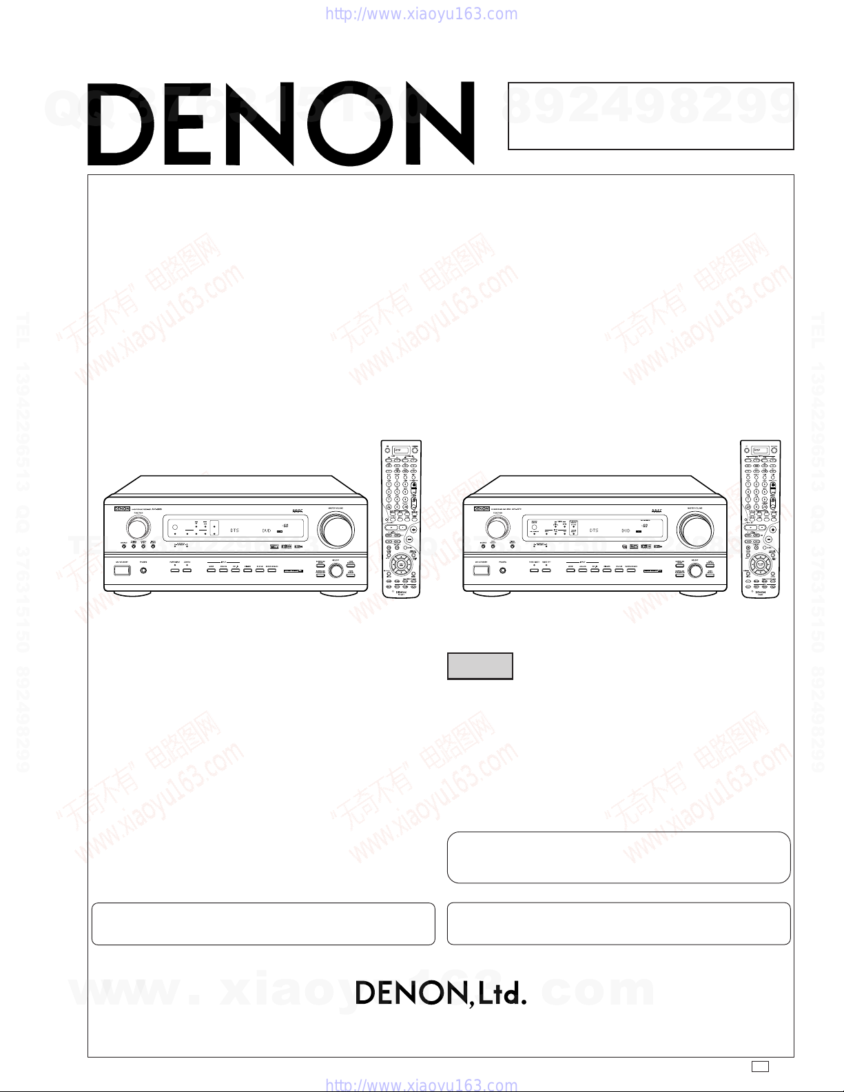
MODEL
TEL 13942296513 QQ 376315150 892498299
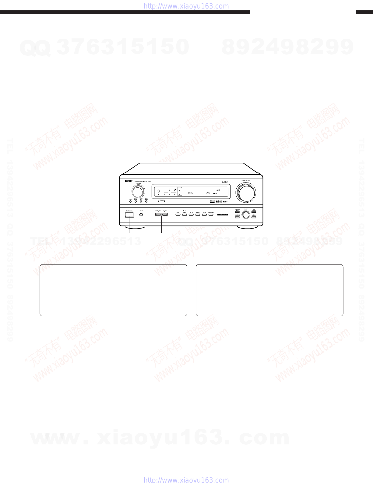
AVR-3803/1083
AVC-3570
AV SURROUND RECEIVER/AMPLIFIER
VOLUME LEVEL
7
3
Q
Q
注 意
TEL
REMOTE
SURROUND
SIGNAL
SENSOR
BACK CH
OUTPUT
DIGITAL
INPUT
SIGNAL
ON / STANDBY
AUTO
DTS
PCM
DETECT
13942296513
AVR-3803 AVC-3570
6
3
1
5
1
5
0
8
9
2
4
9
8
2
9
TEL 13942296513 QQ 376315150 892498299
9
Some illustrations using in this service manual are
slightly different from the actual set.
w
w
w
.
xia
o
16-11, YUSHIMA 3-CHOME, BUNKYOU-KU, TOKYO 113-0034 JAPAN
y
u
1
Telephone: 03 (3837) 5321
サービスをおこなう前に、このサービスマニュアルを
必ずお読みください。本機は、火災、感電、けがなど
に対する安全性を確保するために、さまざまな配慮を
おこなっており、また法的には「電気用品安全法」に
もとづき、所定の許可を得て製造されております。
従ってサービスをおこなう際は、これらの安全性が維
持されるよう、このサービスマニュアルに記載されて
いる注意事項を必ずお守りください。
● 本機の仕様は性能改良のため、予告なく変更すること
があります。
● 補修用性能部品の保有期間は、製造打切後8年です。
● 本文中に使用しているイラストは, 説明の都合上現物
と多少異なる場合があります。
6
3
.
c
o
m
X0155 NC 0211
Page 2
Q
SAFETY PRECAUTIONS
The following check should be performed for the continued protection of the customer and service technician.
7
Q
3
LEAKAGE CURRENT CHECK
Before returning the unit to the customer, make sure you make either (1) a leakage current check or (2) a line to chassis
resistance check. If the leakage current exceeds 0.5 milliamps, or if the resistance from chassis to either side of the
power cord is less than 460 kohms, the unit is defective.
6
3
1
5
1
5
0
8
9
AVR-3803/1083/AVC-3570
4
2
9
8
2
9
9
注 意
注意事項をお守りください!
サービスのとき特に注意を必要とする個所について
TEL 13942296513 QQ 376315150 892498299
は、キャビネット、部品、シャーシなどにラベルや
捺印で、注意事項を表示しています。これらの注意
書きおよび取扱説明書などの注意事項を必ずお守り
ください。
感電に注意!
(1) このセットは、交流電圧が印加されていますの
で、通電時に内部金属部に触れると感電するこ
とがあります。従って通電サービス時には、絶
縁トランスの使用や手袋の着用、部品交換に
は、電源プラグを抜くなどして、感電にご注意
ください。
(2) 内部には、高電圧の部分がありますので、通電
TEL
13942296513
時の取扱には、十分ご注意ください。
指定部品の使用!
セットの部品は難燃性や耐電圧など安全上の特性を
持ったものとなっています。従って交換部品は、使
用されていたものと同じ特性の部品を使用してくだ
さい。特に配線図、部品表に 印で指定されている
安全上重要な部品は必ず指定のものをご使用くださ
い。
サービス、点検時には次のことにご注意願います。
(絶縁チェックの方法)
電源コンセントから電源プラグを抜き、アンテナ
や、プラグなどを外し、電源スイッチを入れま
す。500V絶縁抵抗計を用いて、電源プラグのそれ
ぞれの端子と、外部露出金属部〔アンテナ端子、
ヘッドホン端子、マイク端子、入力端子など〕と
の間で、絶縁抵抗値が1MΩ以上であること、この
値以下のときは、セットの点検修理が必要です。
7
3
Q
Q
注 意
注 意
0
5
1
5
1
3
6
安全上重要な部品について
安全上重要な部品について
8
9
2
4
9
8
2
9
TEL 13942296513 QQ 376315150 892498299
9
部品の取付けや配線の引きまわしは、元どおりに!
安全上、テープやチューブなどの絶縁材料を使用し
たり、プリント基板から浮かして取付けた部品があ
ります。また内部配線は引きまわしやクランパーに
よって発熱部品や高圧部品に接近しないように配慮
されていますので、これらは必ず元どおりにしてく
ださい。
サービス後は安全点検を!
サービスのために取り外したねじ、部品、配線など
が元どおりになっているか、またサービスした個所
の周辺を劣化させてしまったところがないかなどを
点検し、外部金属端子部と、電源プラグの刃の間の
w
w
w
絶縁チェックをおこなうなど、安全性が確保されて
いることを確認してください。
.
xia
o
y
u
本機に使用している多くの電気部品、および機構部品
は安全上、特別な特性を持っています。この特性はほ
とんどの場合、外観では判別つきにくく、また、もと
の部品より高い定格(定格電力、耐圧)を持ったもの
を使用しても安全性が維持されるとは、限りません。
安全上の特性を持った部品は、このサービスマニュア
ルの配線図、部品表につぎのように表示していますの
で、必ず指定されている部品番号のものを使用願いま
す。
1
(1)配線図…
(2)部品表… マークで表示しています。
6
3
.
マークと黒色で薄く塗りつぶすこと
により表示しています。
指定された部品と異なるものを使用し
た場合には、感電、火災などの危険を
c
o
生じる恐れがあります。
m
2
Page 3
AVR-3803/1083/AVC-3570
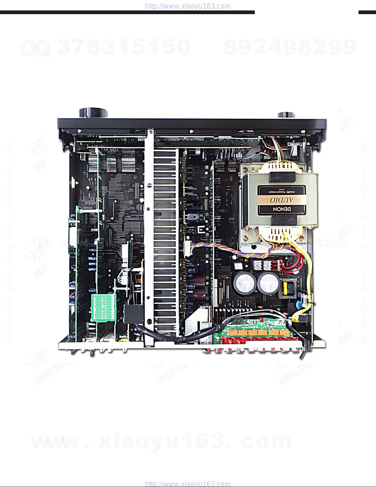
WIRE ARRANGEMENT
If wire bundles are untied or moved to perform adjustment or
Q
TEL 13942296513 QQ 376315150 892498299
parts replacement etc.,be sure to rearrange them neatly as
Q
they were originally bundled or placed afterward.
Otherwise, incorrect arrangement can be a cause of noise
generation.
Wire arrangement viewed from the top
3
7
6
3
1
5
1
5
0
ワイヤー整形図
調整や部品の交換等により、ワイヤー類の結束をはずした
り移動させた場合には、それらの作業が完了した時点でワ
イヤーの整形をおこなってください。正しく整形されてい
ないとノイズ発生の原因となることがあります。
上面からみたワイヤー整形
8
9
2
4
9
8
2
9
9
TEL 13942296513 QQ 376315150 892498299
TEL
13942296513
Q
Q
3
7
6
3
1
5
1
5
0
8
9
2
4
9
8
2
9
9
w
w
w
.
xia
o
y
u
1
6
3
.
c
o
m
3
Page 4
AVR-3803/1083/AVC-3570
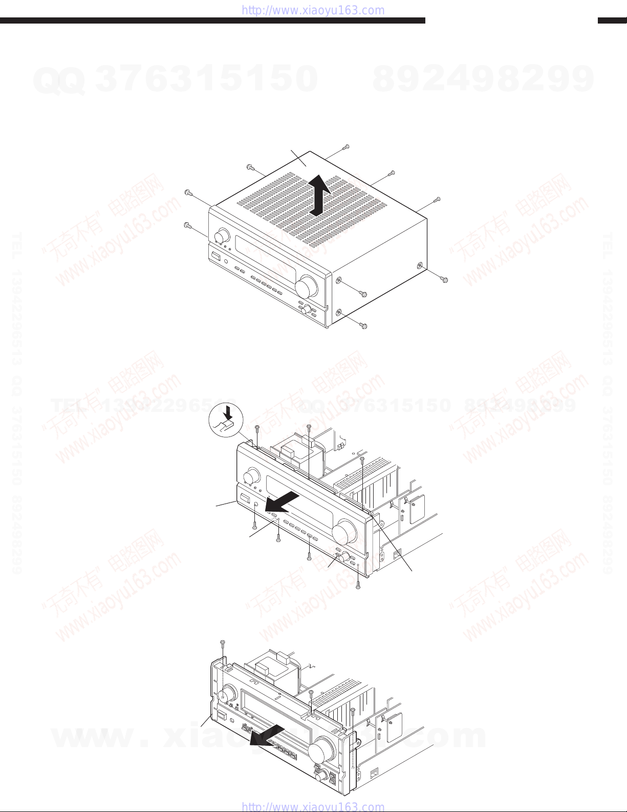
DISASSEMBLY
(Follow the procedure below in reverse order
Q
TEL 13942296513 QQ 376315150 892498299
when reassembling)
Q
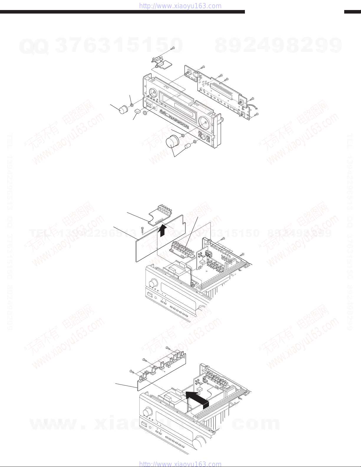
1. Top Cover
Remove 3 screws on the rear and 6 screws on both
sides to detach the Top Cover as shown in the arrow
direction.
2. Front Panel
(1) Remove 7 screws from the top and bottom edges of
(2) Release 4 top and bottom Hooks, then detach the
TEL
7
3
the Front Panel.
Front Panel as shown in the arrow direction.
13942296513
6
3
1
5
1
5
0
Top Cover
Q
各部のはずしかた
(組み立てるときは、逆の順序でおこなってください。)
1. Top Cover
後面からねじ3本、両側からねじ6本をはずしTop Cover
を矢印の方向に取りはずします。
2. Front Panel
(1) Front Panel の上下面からねじ7 本をはずします。
(2) Front Panel を上下で止めている4 個のHook をはず
7
3
Q
4
2
9
8
し、Front Panel を矢印の方向に取りはずします。
0
5
1
5
1
3
6
9
8
9
2
8
4
2
9
8
9
2
9
9
TEL 13942296513 QQ 376315150 892498299
9
3. Inner Panel
Pull out the Inner Panel in the arrow direction after
removing 3 screws.
w
w
w
Front Panel
Inner Panel
.
xia
Hook
Hook
o
y
u
Hook
3. Inner Panel
ねじ3本をはずし、Inner Panelを矢印の方向に取りはず
します。
1
6
3
.
Hook
c
o
m
4
Page 5
AVR-3803/1083/AVC-3570
4. Inner Panel Ass'y
(1) Remove 3 round and 1 square knobs, and unscrew 4
nuts.
7
Q
Q
TEL 13942296513 QQ 376315150 892498299
3
(2) Remove 14 screws fixing each P.W.B.
5. Amp Connect Unit/Component Video Unit
(1) Remove 9 screws to detach Pre-out Unit and
Component Video Unit.
(2) Take off the Amp Connect Unit as shown in the arrow
direction after removing 1 screw.
6
Round Knob
Amp Connect Unit
3
1
5
Nut
Square Knob
Pre-out Unit
1
5
0
Nut
Round Knob
4. Inner Panel Ass'y
(1) Round Knob 3 個とSquare Knob 1 個を引き抜き、4
(2) 各 PWB ユニットを固定しているねじ14 本をはずし
5. Amp Connect Unit/Component Video Unit
(1) ねじ 12 本をはずし、Pre-out Unit とComponent Video
(2) ねじ 1 本をはずし、Amp Connect Unitを矢印の方向に
Component Video Unit
個のNut を取りはずします。
ます。
Unit をはずします。
取りはずします。
8
9
2
4
9
8
2
9
9
TEL 13942296513 QQ 376315150 892498299
TEL
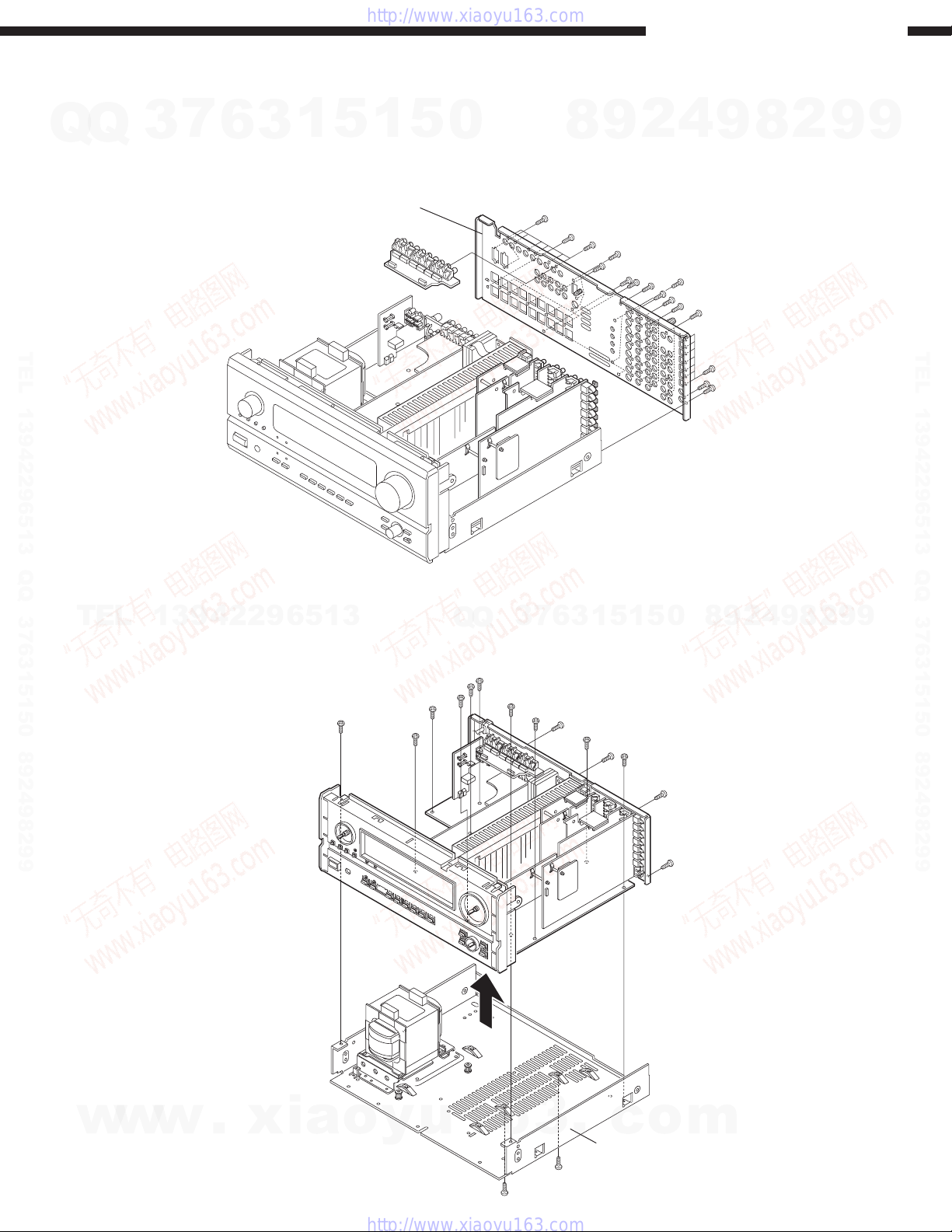
6. Regulator Unit
13942296513
Take off the Regulator Unit as shown in the arrow
direction after removing 11 screws.
Regulator Unit
Q
3
6
7
3
Q
6. Regulator Unit
ねじ11本をはずし、Regulator Unitを矢印の方向に取り
はずします。
1
5
1
5
0
8
9
2
4
9
8
2
9
9
w
w
w
.
xia
o
y
u
1
6
3
.
c
o
m
5
Page 6
AVR-3803/1083/AVC-3570
7. Component-Video/S-Video / C-video /
Audio in / Ext-in VR / Digital/Remote I/O
Q
TEL 13942296513 QQ 376315150 892498299
/ AM FM Tuner Unit
Q
(1) Remove 60 screws to detach the Rear Panel.
(2) Take off the objective P.W.B. upward.
3
7
6
3
1
5
1
5
Rear Panel
0
7. Component-Video/S-Video / C-video /
Audio in / Ext-in VR / Digital/Remote I/O
(1) ねじ 61 本をはずし、Rear Panel を取りはずします。
(2) 目的の P.W.B. を上方向へ取りはずします。
8
9
2
4
9
8
2
9
9
TEL 13942296513 QQ 376315150 892498299
8. How to Check Power / Control Unit with
TEL
13942296513
Power-on
(1) Remove 17 screws fixing to the Chassis.
(2) Pull up the Unit to separate from the Chassis.
Q
8. Powr/Control Unit の通電時チェック方法
Q
6
7
3
(1) 本体を Chassis へ取り付けているねじ17 本をはずし
ます。
(2) 本体を上方向へ Chassis から分離させます。
3
1
5
1
5
0
8
9
2
4
9
8
2
9
9
w
w
w
.
xia
o
y
u
1
6
3
.
Chassis
c
o
m
6
Page 7
AVR-3803/1083/AVC-3570
CAUTION IN SERVICING
Initializing AV SURROUND RECEIVER
Q
TEL 13942296513 QQ 376315150 892498299
Q
AV SURROUND RECEIVER initialization should be
performed when the µcom, peripheral parts of µcom, and
DSP P.W.B. are replaced.
1. Switch off the unit and remove the AC cord from the
2. Hold the following PURE DIRECT button and ZONE
3. Check that the entire display is flashing with an
7
3
wall outlet.
2 button, and plug the AC cord into the outlet.
interval of about 1 second, and release your fingers
from the 2 buttons and the microprocessor will be
initialized.
6
3
1
5
1
5
REMOTE
SENSOR
ON / STANDBY
SIGNAL
DIGITAL
INPUT
AUTO
DTS
PCM
0
サービス時の注意事項
AV サラウンドアンプの初期化について
マイコンやマイコン周辺部品、DSP基板等を交換し
た場合は、AVサラウンドアンプの初期化を行って下
さい。
1. 電源ボタンを押してスタンバイ状態にしてから、
2. PURE DIRECT ボタンとVIDEO OFF ボタンを同
3. ディスプレイ表示が約1 秒間隔で点滅するのを確
SURROUND
BACK CH
OUTPUT
SIGNAL
DETECT
4
2
9
8
壁の電源コンセントから電源コードを抜きます。
時に押しながら、電源プラグをコンセントに差し
込みます。
認後、2 つのボタンから指を離します。
●マイコンが初期化されます。
VOLUME LEVEL
9
8
2
9
9
TEL 13942296513 QQ 376315150 892498299
1 2
TEL
13942296513
Note: If step 3 does not work, start over from step 1.
All user settings will be lost and this factory
setting will be recovered when this initialization
mode.
So make sure to memorize your setting for
restoring after the initialization.
Q
4
2
9
8
0
5
1
5
1
3
6
7
3
Q
注意: 上記3の状態にならない場合は、もう一度操作1
からやり直してください。
初期化を行うとお客様が設定した内容が工場出
荷状態に戻りますので、あらかじめ設定内容を
控えておき初期化後再設定してください。
9
8
2
9
9
w
w
w
.
xia
o
y
u
1
6
3
.
c
o
m
7
Page 8
AVR-3803/1083/AVC-3570
ADJUSTMENT
Audio Section
7
Q
Q
TEL 13942296513 QQ 376315150 892498299
TEL
3
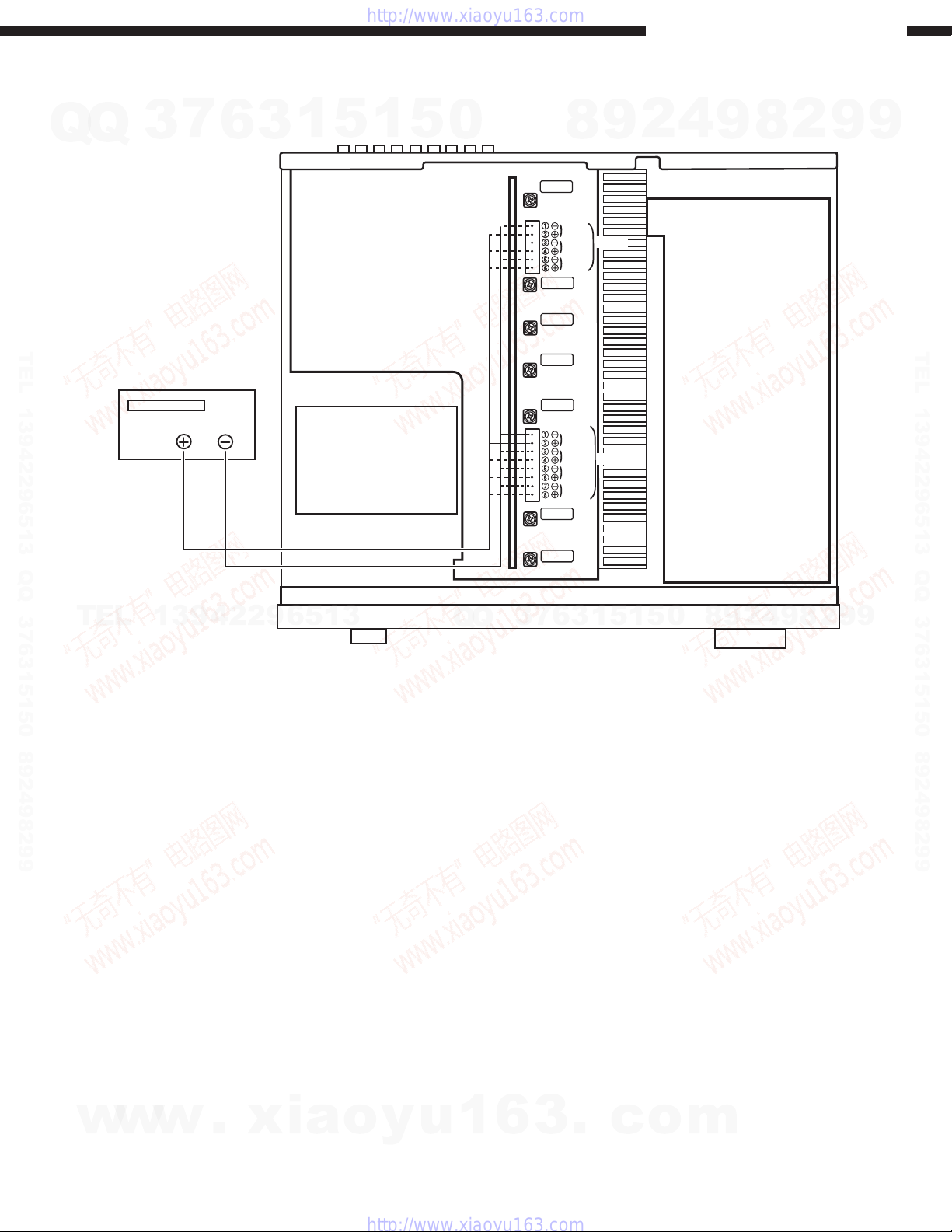
Idling Current (1U-3469-1)
Required measurement equipment: DC Voltmeter
Preparation
(1) Avoid direct blow from an air conditioner or an electric
fan, and adjust the unit at normal room tempereture 15
°C ~ 30 °C (59 °F ~ 86 °F).
(2) Presetting
POWER (Power sourse switch) OFF
SPEAKER (Speaker terminal) No load
(Do not connect speaker, dummy resistor, etc.)
Adjustment
(1) Remove top cover and set VR101, VR102, VR201,
VR301, VR302, VR401, VR402, on 1U-3469-1 (Power
Unit) at fully counterclockwise ( ).
(2) Connect DC Voltmeter to test points (FRONT-Lch:
TP301
CENTER ch: TP301 3 4 pin, SURROUND-Lch: TP101
SURROUND BACK-Lch: TP301
BACK-Rch: TP301 5 6 pin).
(3) Connect power cord to AC Line, and turn power switch
"ON".
(4) Presetting.
(5) Allow 2 minutes, and turn VR101 clockwise ( ) to
adjust the TEST POINT voltage to 6.5 mV ±0.5 mV DC.
(6) After 10 minutes from preset, turn VR101 to set the
voltage to 8 mV ±0.5 mV DC.
(7) Adjust the Variable Resistors of other channels in the
same way.
(8) After 5 minutes from (6), turn VR101 to set the voltage to
8 mV ±0.5 mV DC.
(9) Adjust the Variable Resistors of other channels in the
same way.
1 2
3 4
pin, SURROUND-Rch: TP101 1 2 pin,
MASTER VOLUME : "---" counterclockwise ( min.)
MODE : 7CH STEREO
FUNCTION : CD
13942296513
6
pin, FRONT-Rch: TP101 5 6 pin,
3
1
5
1
7 8
pin, SURROUND
5
0
Q
調整
オーディオセクション
アイドリング電流の調整 (1U-3469-1)
調整に必要な測定器: DC Voltmeter
準備
(1) セットをクーラ、扇風機のそばなど風通しの良い場所を
避け、通常の使用状態に置きます。セットの周囲温度は
15 〜30℃、湿度は常湿とします。
(2) プリセット
電源スイッチ OFF
スピーカ端子 無負荷
調整
(1) 上カバーをはずし、1U-3469-1(パワーユニット)の
VR101, VR102, VR201, VR301, VR302, VR401, VR402
を反時計方向 ( ) に回し切った状態にセットします。
(2) テストポイント (FRONT-Lch: TP301
Rch: TP101
SURROUND-Lch: TP101 3 4 pin, SURROUND-Rch:
TP101 1 2 pin, SURROUND BACK-Lch: TP301 7
pin, SURROUND BACK-Rch: TP301 5
Voltmeter を接続します。
(3) 電源コードを AC100V(95 〜105V の範囲でも可)に接
続し、電源スイッチを"ON" にします。
(4) ON 後、次のようにセットします。
MASTER VOLUME(音量調節つまみ)→反時計方向
7
3
Q
SPEAKER(スピーカ端子)→無負荷(スピーカ、
(5) 2 分以内にVR101 を時計方向 (
トの電圧を次のように調整します。
(6) 予備調整から 10 分後VR101 を回し、次のように電圧を
設定します。
(7) 同じ方法で各チャネルの可変抵抗を調整します。
(8) (6)項設定から 5 分後VR101 を回し、次のように電圧を
設定します。
(9) 同じ方法で各チャネルの可変抵抗を調整します。
4
2
9
8
(スピーカ・ダミー抵抗器などを接続しない。)
5 6
pin, CENTER ch: TP301 3 4 pin,
( ) に回す、最小の状態にする。
0
5
1
5
1
3
6
ダミー抵抗器などを接続しない。)
MODE : 7CH STEREO
FUNCTION : CD
6.5mV ±0.5mV DC
8mV ±0.5mV DC
8mV ±0.5mV DC
9
2
9
8
) に回しテストポイン
8
1 2
6
4
pin) にDC
9
2
pin, FRONT-
8
9
2
9
9
TEL 13942296513 QQ 376315150 892498299
8
9
w
w
w
.
xia
o
y
u
1
6
3
.
c
o
m
8
Page 9
AVR-3803/1083/AVC-3570
7
Q
Q
TEL 13942296513 QQ 376315150 892498299
3
DC Voltmeter
6
3
1
5
1
5
0
SR ch
VR302
SL ch
VR301
FR ch
VR102
FL ch
VR101
C ch
VR201
SBR ch
VR402
SBL ch
VR401
8
SR ch
SL ch
FR ch
FL ch
C ch
SBR ch
SBL ch
9
TP101
TP301
2
4
9
8
2
9
9
TEL 13942296513 QQ 376315150 892498299
TEL
13942296513
6
7
3
Q
Q
Audio Section
3
1
5
1
5
0
8
9
2
4
9
8
2
9
9
w
w
w
.
xia
o
y
u
1
6
3
.
c
o
m
9
Page 10
AVR-3803/1083/AVC-3570
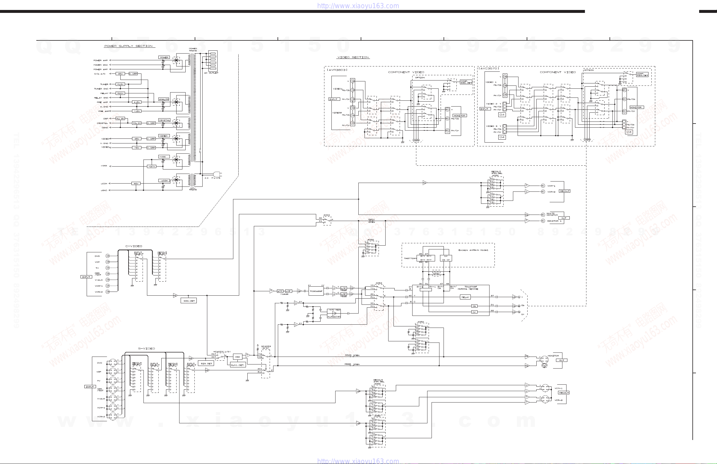
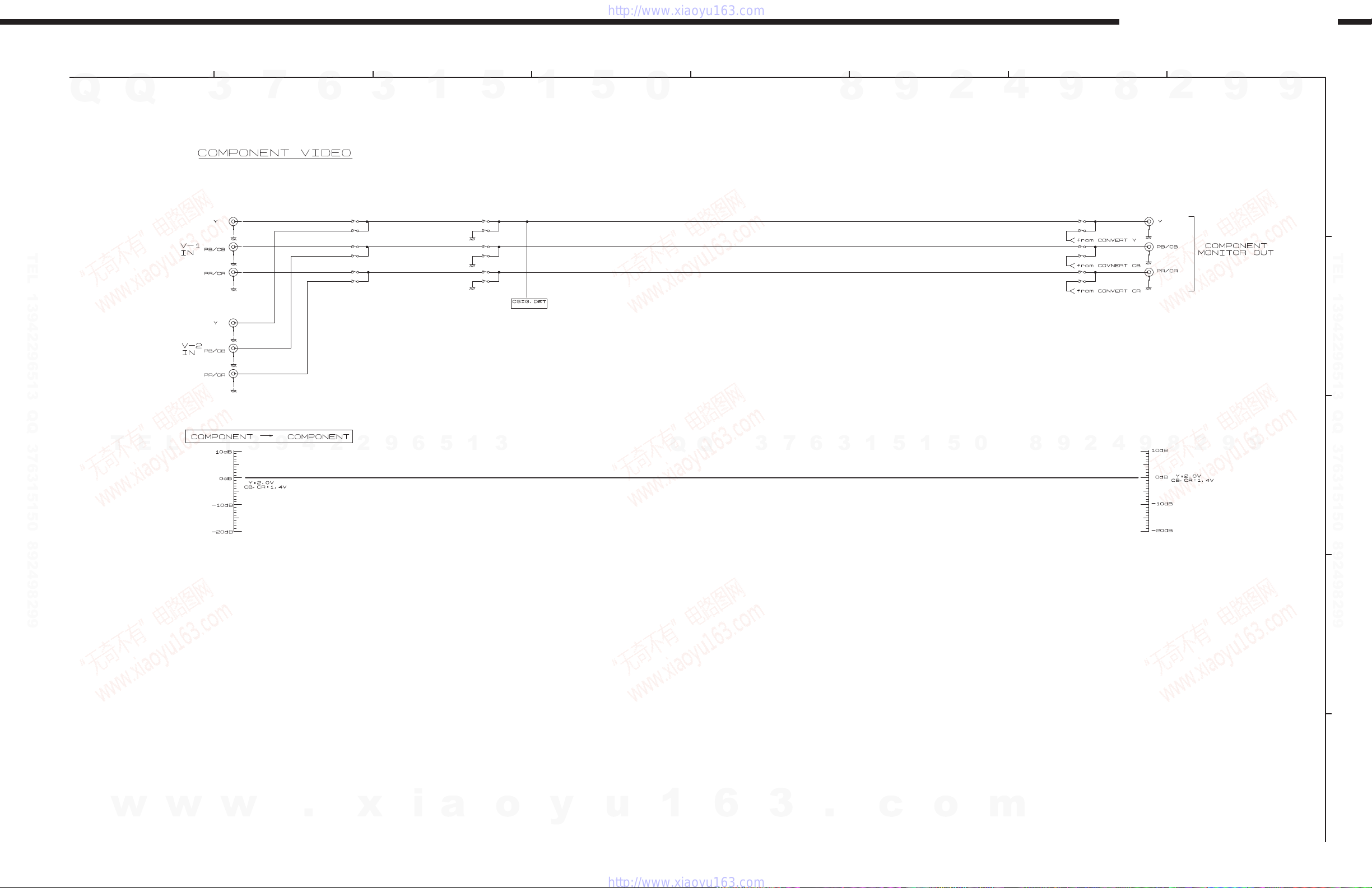
Video Section
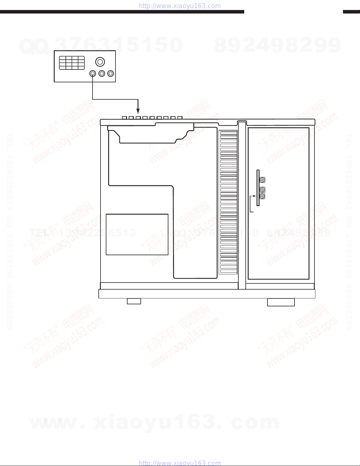
Component Video Level Adjustment
Q
TEL 13942296513 QQ 376315150 892498299
Required measurement equipment etc: Oscilloscope, DVD
Q
VIDEO PLAYER (ex: DVD-1500)
Test Disc: DVD T-S01
Preparation
(1) Avoid direct blow from an air conditioner or an electric
fan, and adjust the unit at normal room temperature 15
°C ~ 30 °C (59 °F ~ 86 °F).
(2) Playback the color-bar 75% of the Test Disc (Title 12)
using the DVD Video Player, and check that Y and C
levels of the S terminal output are within the specified
output levels.
If they are out of the specified levels, adjust with the
variable resister inside of the unit.
(3) Presetting
POWER (Power source switch) OFF
SPEAKER (Speaker terminal) No load
DVD (Video terminal) No input
Adjustment
(1) Remove top cover and set VR101, VR102, VR103 on
1U-3475-1 (Convert Unit) at fully counterclockwise (
(2) Connect a pin-plug terminated with 75-ohms to Y(Cb,
Cr) of the Component Video Monitor Output, and hook
up the Oscilloscope's probe to both ends of the pin-plug.
(3) Connect S terminal output of the DVD Player with the
DVD input terminal of the Receiver.
(4) Connect power cord to AC Line, and turn power switch
TEL
"ON".
(5) Presetting
FUNCTION: DVD
(6) Turn VR101 clockwise ( ) to adjust the
COMPONENT VideoY voltage (except H.Sync) to 714
±50 mVp-p. (Refer to Fig.1)
(7) Adjust the Variable Resistors of Cb: VR102 and Cr:
VR103 in the same way. (Refer to Fig. 2, 3)
7
3
(Do not connect speaker, dummy resistor, etc.)
6
13942296513
Playback the color-bar 75% of the Test Disc (Title 12)
Cb,Cr: 486±50 mVp-p. (U.S.A. & Canada model)
525±50 mVp-p. (Others)
3
1
5
1
5
0
Q
ビデオセクション
コンポーネントビデオレベルの調整
調整に必要な測定器: Oscilloscope, DVD VIDEO PLAYER
テストディスク: DVD T-S01
準備
(1) セットをクーラ、扇風機のそばなど風通しの良い場所を
避け、通常の使用状態に置きます。セットの周囲温度は
15 〜30℃、湿度は常湿とします。
(2) DVD VIDEO PLAYER でテストディスクのカラーバー
75%(Title12)を再生し、S 端子出力Y、C レベルが正規
の出力レベルであることを確認する。正規の出力レベル
ではない場合は、セット内部の可変抵抗器で調整してく
ださい。
(3) プリセット
電源スイッチ OFF
スピーカ端子 無負荷
DVD 入力端子 無入力
調整
(1) 上カバーをはずし、1U-3475-1(コンバートユニット)
).
Q
のVR101, VR102, VR103 を反時計方向 ( ) に回し切っ
た状態にセットします。
(2) コンポーネントビデオモニターアウトの Y(Cb, Cr)に 75
Ωで終端したピンプラグをを接続し、その両端を
Oscilloscope のプローブでつまみます。
(3) DVD VIDEO PLAYER のS 端子出力を本機のDVD 入力
端子に接続します。
(4) 電源コードを電源コンセントに接続し、電源スイッチを
7
3
"ON" にします。
(5) ON 後、次のようにセットします。
本機のFUNCTION をDVD にする。
テスクディスクのカラーバー75%(Title12)を
(6) VR101 を時計方向 (
Y(H.Sync を除く)の電圧を調整します。(Fig.1 参照)
(7) 同じ方法でCb: VR102 、 Cr: VR103の可変抵抗器を調整
します。(Fig.2、3 参照)
4
8
(スピーカ・ダミー抵抗器などを接続しない。)
3
6
再生する。
(例: DVD-1500)
0
5
1
5
1
) に回しコンポーネントビデオ
714mV ±50mVp-p
Cb,Cr: 525±50 mVp-p.
2
9
9
8
9
2
8
4
2
9
8
9
2
9
9
TEL 13942296513 QQ 376315150 892498299
9
w
w
w
.
xia
o
y
u
1
6
3
.
c
o
m
10
Page 11
Q
Q
Oscilloscope
7
3
6
3
1
5
1
5
0
8
9
AVR-3803/1083/AVC-3570
2
4
9
8
2
9
9
TEL 13942296513 QQ 376315150 892498299
TEL
13942296513
Q
Q
3
7
6
3
1
5
1
Cb
Component Video Y
0
5
VR103Cr
VR102
VR101
8
9
2
4
9
8
2
9
TEL 13942296513 QQ 376315150 892498299
9
w
w
w
.
xia
Video Section
o
y
u
1
6
3
.
c
o
m
11
Page 12
AVR-3803/1083/AVC-3570
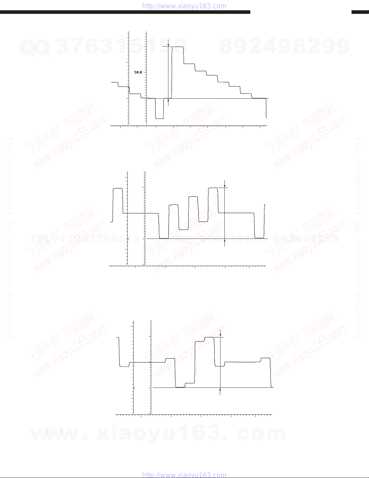
Volts
IRE:FLT
7
Q
Q
TEL 13942296513 QQ 376315150 892498299
3
6
1
3
-20.0 -10.0 0.0
Volts
0.5
5
0.5
0.5
IRE:FLT
Y-Signal
100.0
1
5
0
714±50mV
p-p
0.0
10.0
20.0 30.0
Fig.1 Component Video Y signal
50.0
4
2
9
8
40.0 50.0 60.0
486±50mV (U.S.A. & Canada model)
p-p
525±50mV (Others)
p-p
9
8
2
9
9
TEL 13942296513 QQ 376315150 892498299
TEL
0.0
-0.5
Volts
0.5
0.0
-50.0
0.0
IRE:FLT
13942296513
0.0
50.0
-50.0
0.0
Q
Q
20.0
Fig.2 Cb signal
40.0
3
1
5
1
3
6
7
60.0
486±50mV (U.S.A. & Canada model)
525±50mV (Others)
80.0
p-p
p-p
5
0
8
9
2
4
9
8
2
9
9
w
w
w
.
xia
-0.5
0.0
o
y
20.0
Fig.3 Cr signal
u
1
40.0
6
3
.
60.0
c
80.0
o
m
12
Page 13
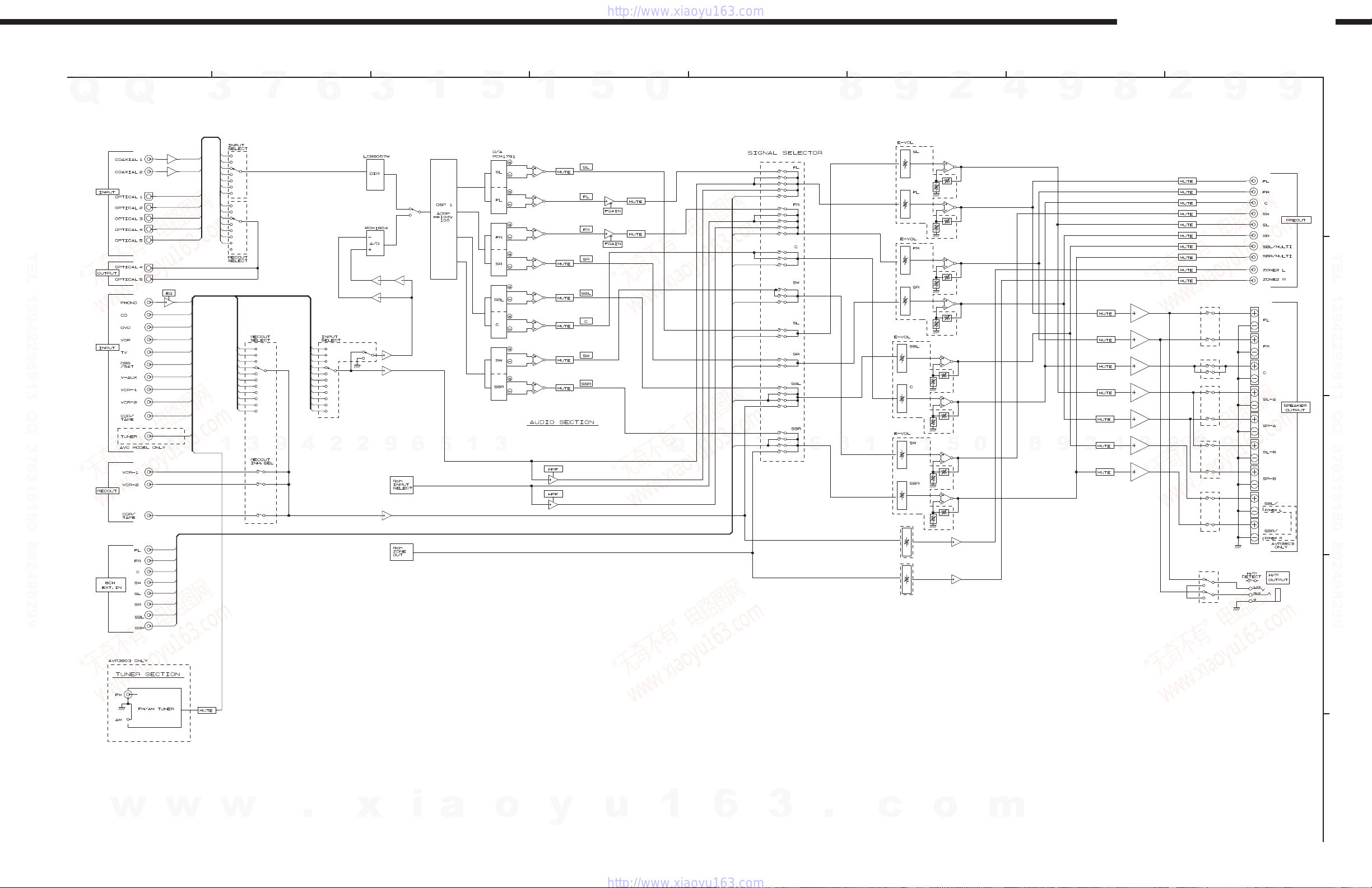
BLOCK DIAGRAMS (1/2)
AVR-3803/AVR-1083/AVC-3570
1
Q
TEL 13942296513 QQ 376315150 892498299
Q
3
7
2
6
3
1
3
5
1
4
5
0
5
8
9
2
4
9
76
8
2
9
8
9
A
TEL 13942296513 QQ 376315150 892498299
B
T
E
L
1
3
9
4
2
2
9
6
5
1
3
Q
Q
3
7
6
3
1
5
1
5
0
8
9
2
4
9
8
2
9
9
C
D
w
w
w
.
x
i
a
o
y
u
1
6
3
.
c
o
E
m
13
Page 14
BLOCK DIAGRAMS (2/2)
AVR-3803/AVR-1083/AVC-3570
1
Q
TEL 13942296513 QQ 376315150 892498299
Q
3
7
2
6
3
1
5
4
0
3
5
1
5
8
9
2
4
9
76
8
2
9
8
9
A
TEL 13942296513 QQ 376315150 892498299
B
T
E
L
1
3
9
4
2
2
9
6
5
1
3
Q
Q
3
7
6
3
1
5
1
5
0
8
9
2
4
9
8
2
9
9
C
D
w
w
w
.
x
i
a
o
y
u
1
6
3
.
c
o
E
m
14
Page 15
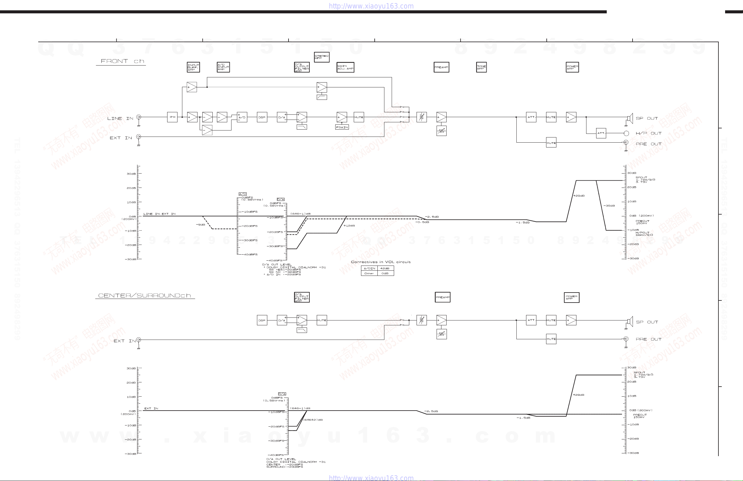
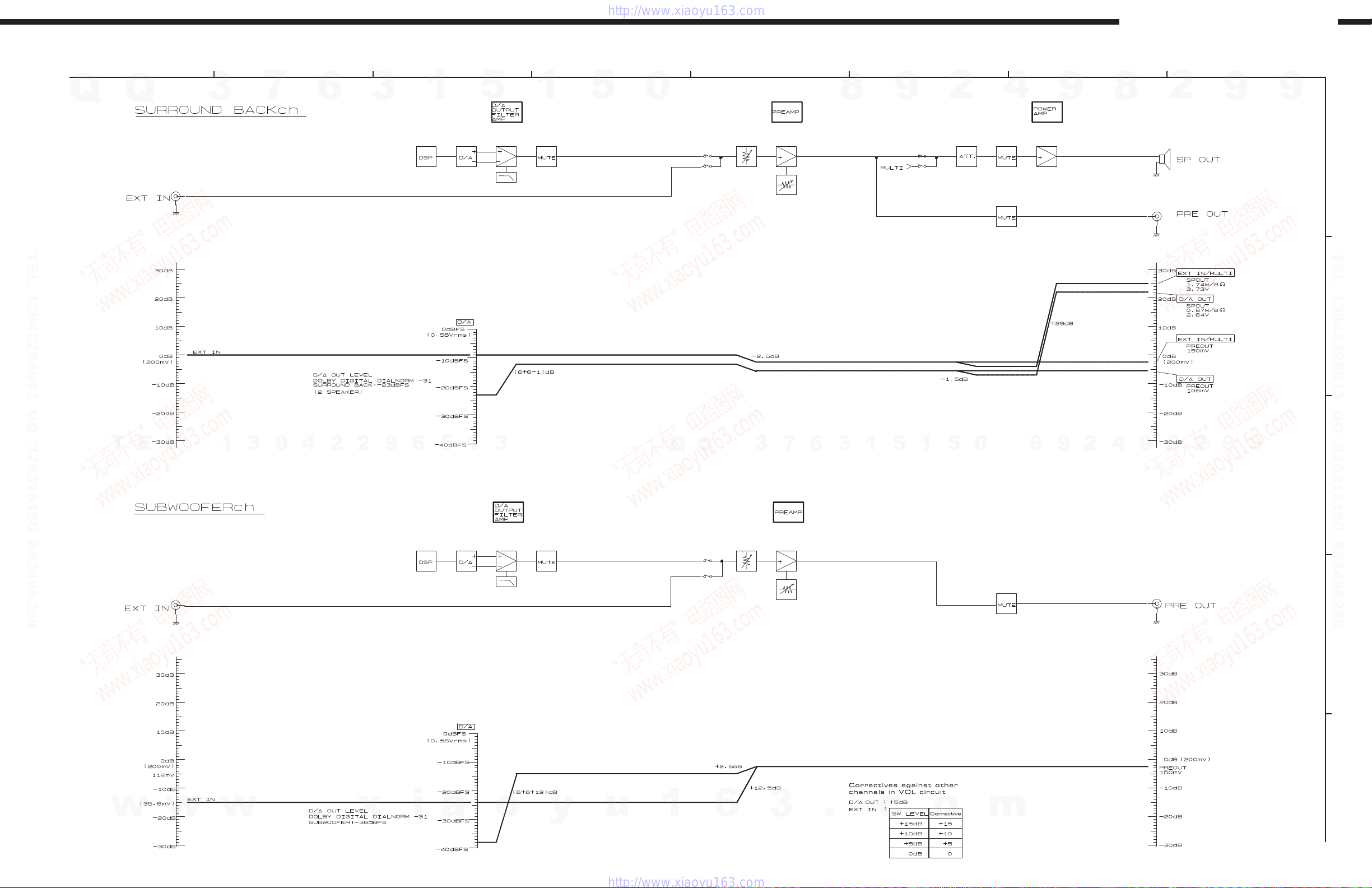
LEVEL DIAGRAMS (1/5)
AVR-3803/AVR-1083/AVC-3570
1
AUDIO SECTION (1/2)
Q
TEL 13942296513 QQ 376315150 892498299
Q
3
7
2
6
3
1
5
4
0
3
5
1
5
8
9
2
4
9
76
8
2
9
8
9
A
TEL 13942296513 QQ 376315150 892498299
B
T
E
L
1
3
9
4
2
2
9
6
5
1
3
Q
Q
3
7
6
3
1
5
1
5
0
8
9
2
4
9
8
2
9
9
C
D
w
w
w
.
x
i
a
o
y
u
1
6
3
.
c
o
E
m
15
Page 16
LEVEL DIAGRAMS (2/5)
AVR-3803/AVR-1083/AVC-3570
1
AUDIO SECTION (2/2)
Q
TEL 13942296513 QQ 376315150 892498299
Q
3
7
2
6
3
1
5
4
0
3
5
1
5
8
9
2
4
9
76
8
2
9
8
9
A
TEL 13942296513 QQ 376315150 892498299
B
T
E
L
1
3
9
4
2
2
9
6
5
1
3
Q
Q
3
7
6
3
1
5
1
5
0
8
9
2
4
9
8
2
9
9
C
D
w
w
w
.
x
i
a
o
y
u
1
6
3
.
c
o
E
m
16
Page 17
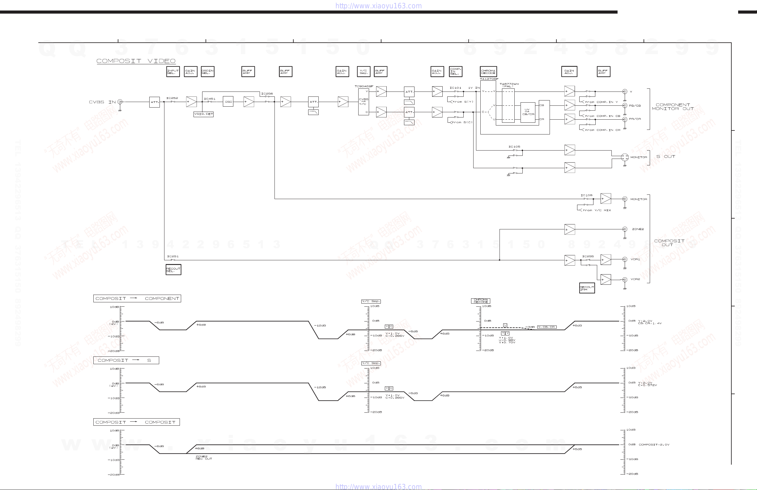
LEVEL DIAGRAMS (3/5)
AVR-3803/AVR-1083/AVC-3570
1
VIDEO SECTION (1/3)
Q
TEL 13942296513 QQ 376315150 892498299
Q
3
7
2
6
3
1
5
4
0
3
5
1
5
8
9
2
4
9
76
8
2
9
8
9
A
TEL 13942296513 QQ 376315150 892498299
B
T
E
L
1
3
9
4
2
2
9
6
5
1
3
Q
Q
3
7
6
3
1
5
1
5
0
8
9
2
4
9
8
2
9
9
C
D
w
w
w
.
x
i
a
o
y
u
1
6
3
.
c
o
E
m
17
Page 18
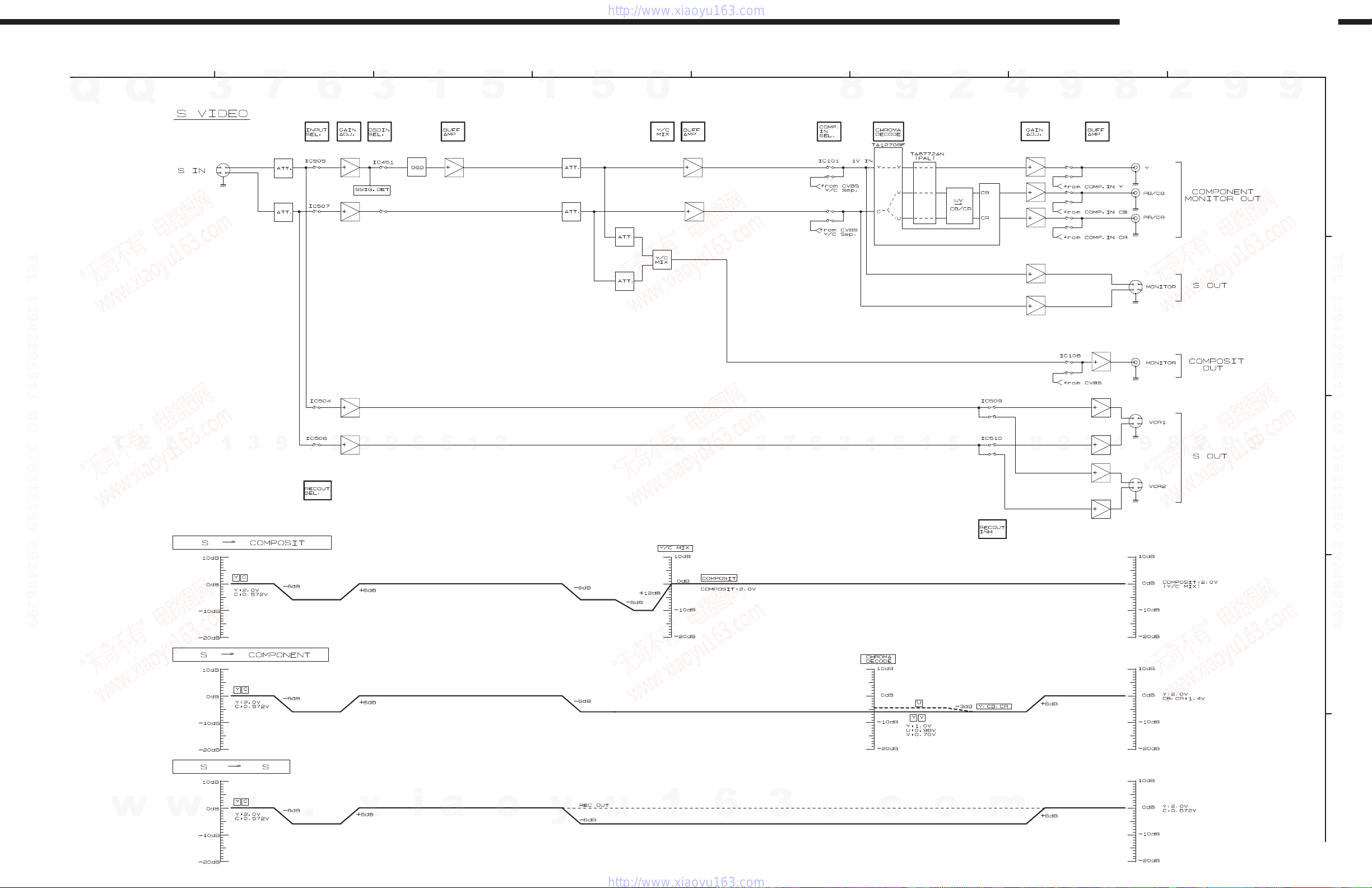
LEVEL DIAGRAMS (4/5)
AVR-3803/AVR-1083/AVC-3570
1
VIDEO SECTION (2/3)
Q
TEL 13942296513 QQ 376315150 892498299
Q
3
7
2
6
3
1
5
4
0
3
5
1
5
8
9
2
4
9
76
8
2
9
8
9
A
TEL 13942296513 QQ 376315150 892498299
B
T
E
L
1
3
9
4
2
2
9
6
5
1
3
Q
Q
3
7
6
3
1
5
1
5
0
8
9
2
4
9
8
2
9
9
C
D
w
w
w
.
x
i
a
o
y
u
1
6
3
.
c
o
E
m
18
Page 19
LEVEL DIAGRAMS (5/5)
AVR-3803/AVR-1083/AVC-3570
1
VIDEO SECTION (3/3)
Q
TEL 13942296513 QQ 376315150 892498299
Q
3
7
2
6
3
1
5
4
0
3
5
1
5
8
9
2
4
9
76
8
2
9
8
9
A
TEL 13942296513 QQ 376315150 892498299
B
T
E
L
1
3
9
4
2
2
9
6
5
1
3
Q
Q
3
7
6
3
1
5
1
5
0
8
9
2
4
9
8
2
9
9
C
D
w
w
w
.
x
i
a
o
y
u
1
6
3
.
c
o
E
m
19
Page 20
CLOCK FLOW & WAVE FORM IN DIGITAL BLOCK
㽳㽳
㽴㽴
㽳㽳㽳㽳
/
Wave form
Q
Q
3
7
6
3
1
CH1: D-DATA
(IC510 (5) )
1
5
1
5
0
8
9
2
4
9
8
AVR-3803/1083/AVC-3570
2
9
9
TEL 13942296513 QQ 376315150 892498299
2
CH1: DATA
T
E
L
1
3
9
4
2
2
9
CH2: fs
CH3: 64fs
3
CH1: DATA
6
5
1
㽲㽲㽲㽲㽳
INPUT
INPUT
INPUTINPUT
SELECTOR
SELECTOR BUFFER
SELECTORSELECTOR
IC5㪈3
IC5㪈3 IC522
IC5㪈3IC5㪈3
INPUT
INPUT
INPUTINPUT
COAXIAL-㪈
COAXIAL-㪈 (3) RDATA(2㪈)(㪈㪈)- -(9) (64)SD0A
COAXIAL-㪈COAXIAL-㪈
COAXIAL-2
COAXIAL-2 (2) SLRCK(23) (㪈3)- -(7) (38)SFS2 (㪈)fs
COAXIAL-2COAXIAL-2
OPTICAL-㪈
OPTICAL-㪈 (㪈2) (5) (4)RX2 (39)SFS3 (2)64fs SLch
OPTICAL-㪈OPTICAL-㪈
OPTICAL-2
OPTICAL-2 (㪈3) SBCK(22) (㪈5)- -(5) (7)SCLK2 (3)DATA FLch
OPTICAL-2OPTICAL-2
OPTICAL-3
OPTICAL-3 (㪈4) (㪈7)- -(3) (54)SCLK3 (5)256fs
OPTICAL-3OPTICAL-3
OPTICAL-4
OPTICAL-4 (㪈5) RMCK(㪈6) (4)- -(㪈6)
OPTICAL-4OPTICAL-4
OPTICAL-5
OPTICAL-5 (㪈) (2)- -(㪈8) (50)SCLK0
OPTICAL-5OPTICAL-5
3
OUTPUT
OUTPUT
OUTPUTOUTPUT
OPTICAL-4
OPTICAL-4
OPTICAL-4OPTICAL-4
OPTICAL-5
OPTICAL-5 (㪈)fs
OPTICAL-5OPTICAL-5
SN74HC
SN74HC SN74LV
SN74HC SN74HC
㪈5㪈APW
㪈5㪈APW 244APW
㪈5㪈APW㪈5㪈APW
OUTPUT
OUTPUT (52)SFS㪈 (㪈)fs
OUTPUTOUTPUT
SELECTOR
SELECTOR ADIN(24) SD2A(37) (2)64fs FRch
SELECTORSELECTOR
Q
Q
IC5㪈4
IC5㪈4 SD3A(23) (5)256fs
IC5㪈4IC5㪈4
SN74HC
SN74HC
SN74HC SN74HC
㪈5㪈APW
㪈5㪈APW
㪈5㪈APW㪈5㪈APW
(3) (㪈5)DATA
(2) 24.576MHz
(㪈2) IC52㪈
(㪈3) (5) FXC0
(㪈4) -03
(㪈5) (3) (5)256fs
(㪈)
24.576MHz (㪈6)BCK
24.576MHz24.576MHz
DIR
DIR DSP
DIRDIR
IC520
IC520
IC520IC520
LC89057W
LC89057W
LC89057WLC89057W
DATA
fs
64fs
256fs
6
64fs
fs
3
A/D CONVERTER
A/D CONVERTER IC526
A/D CONVERTERA/D CONVERTER
RBCK(㪈7) (6)- -(㪈4) (2㪈)SCLK㪈
RLRCK(20) (8)- -(㪈2) (20)SFS0
(29)XIN SD2B(22) (3)DATA SRch
7
3
IC52㪈 (㪈7)LRCK (㪈)fs
IC52㪈IC52㪈
FXC0 SYSCK(㪈8) (2)64fs SBLch
FXC0FXC0
-03 (3)DATA Cch
-03-03
BUFFER
BUFFERBUFFER
IC522
IC522IC522
SN74LV
SN74LVSN74LV
244APW
244APW244APW
5
1
IC5㪈9
IC5㪈9
IC5㪈9IC5㪈9
PCM㪈804
PCM㪈804
PCM㪈804PCM㪈804
㽳㽴
DSP
DSPDSP
IC80㪈
IC80㪈
IC80㪈IC80㪈
ADSST-MEL㪈00
ADSST-MEL㪈00
ADSST-MEL㪈00ADSST-MEL㪈00
4
2
9
1
5
0
8
SD3B (8)
9
㽴
D/A CONVERTER
D/A CONVERTER
A CONVERTERD/A CONVERTER
D
IC523
IC523
IC523IC523
PCM㪈79㪈
PCM㪈79㪈
PCM㪈79㪈PCM㪈79㪈
IC524
IC524
IC524IC524
PCM㪈79㪈
PCM㪈79㪈
PCM㪈79㪈PCM㪈79㪈
9
2
8
IC525
IC525
IC525IC525
PCM㪈79㪈
PCM㪈79㪈
PCM㪈79㪈PCM㪈79㪈
IC526
IC526IC526
PCM㪈79㪈
PCM㪈79㪈
PCM㪈79㪈PCM㪈79㪈
(2)64fs SWch
(3)DATA SBRch
(5)256fs
TEL 13942296513 QQ 376315150 892498299
9
w
w
w
.
CH2: fs
CH3: 64fs
x
CH4: 256fs
i
a
o
y
u
1
6
3
.
c
o
m
20
Page 21
CHECK WITH TEST MODE テストモードによるチェック方法
µµ
µcom/DSP Error Display Mode
µµ
Q
1. Operation Spec
µµ
µcom version display mode:
µµ
When the following conditions are satisfied at its starting state, error information is displayed before version information.
Q
3
7
6
3
1
5
1
5
0
マイコン・DSP エラー表示モード
8
1. 動作仕様
マイコンバージョン表示モード:
起動状態にて下記の条件に該当した場合は、バージョン情報表示の前にエラー情報を表示します。
9
2
4
9
8
AVR-3803/1083/AVC-3570
2
9
9
Starting method (same as
While pressing 2 buttons, "DIMMER (S11)" and "SURROUND BACK (S14)", plug the AC cord to the wall outlet.
Then, press "STATUS" button to display the following information on the FL Display.
2. Display Order
TEL 13942296513 QQ 376315150 892498299
Error information → Main-µcom version information → Sub-µcom version information → DSP version information
3. Display
Any one of the following list is displayed, in the priority of
Condition State Display
1
Sub-µcom NG No response from Sub-µcom "□SUB□□ERROR□01□"
2
DIR NG No response from DIR "□DIR□□ERROR□01□"
3
DSP NG When DSP boot, executing DSP reset
T
E
L
µµ
µcom version display):
µµ
1
2 3
4
.
makes no change to BUSY port "L".
No change to BUSY port "L" before issuing DSP command. "□DSP□ERROR□02□"
When DSP data read, executing WRITE="L"
1
3
9
4
2
2
makes no change to ACK="H".
When DSP data read, executing REQ="L"
makes no change to ACK="L".
When DSP data write, executing WRITE="H"
makes no change to ACK="H".
When DSP data write, executing REQ="L"
makes no change to ACK="L".
When DSP special code boot, executing DSP reset
makes no change to BUSY port "L".
No change to BUSY port "L" before issuing
DSP special read command.
9
6
5
1
"□DSP□ERROR□01□"
"□DSP□ERROR□03□"
3
"□DSP□ERROR□04□"
"□DSP□ERROR□05□"
"□DSP□ERROR□06□"
"□DSP□ERROR□11□"
"□DSP□ERROR□12□"
Q
起動方法(マイコンバージョン表示と同様):
"DIMMER"(S11), "SURROUND BACK"(S14)の2つのボタンを押した状態で、ACコードを差し込みます。
その後、STATUSボタンを押すと下表の内容がFL Displayに表示されます。
2. 表示順序
エラー情報→メインマイコンバージョン情報→サブマイコンバージョン情報→DSPバージョン 情報
3. 表示条件
1
1 234
0
5
。
8
9
2
4
"□DSP□ERROR□01□"
9
2
8
9
"□DSP□ERROR□11□"
"□DSP□ERROR□12□"
下表のいずれかを表示します。表示の優先順は、
条件 状態 表示内容
1
SUBマイコンがNG SUBマイコンからの応答がない "□SUB□□ERROR□01□"
2
DIRがNG DIRからの応答がない "□DIR□□ERROR□01□"
3
DSPがNG DSPコードブート時、DSPリセットを実行しても
BUSYポートが"L"にならない
DSPコマンド発行前に、BUSYポートが"L"にならない "□DSP□ERROR□02□"
DSPデータリード時、WRITE="L"としてもACK="H"とならない "□DSP□ERROR□03□"
5
1
3
6
7
Q
4
3
SUB/DSP共にOK (表示せずにバージョン表示を行う)
DSPデータリード時、REQ="L"としてもACK="L"とならない "□DSP□ERROR□04□"
DSPデータライト時、WRITE="H"としてもACK="H"とならない "□DSP□ERROR□05□"
DSPデータライト時、REQ="L"としてもACK="L"とにならない "□DSP□ERROR□06□"
DSPスペシャルコードブート時、DSPリセットを実行しても
BUSYポートが"L"にならない
DSPスペシャルリードコマンド発行前に、
BUSYポートが"L"にならない
DSPバージョンリード前に、BUSYポートが"L"にならない "□DSP□ERROR□13□"
TEL 13942296513 QQ 376315150 892498299
9
4
Both SUB/DSP OK
w
w
No change to BUSY port "L" before DSP version read. "□DSP□ERROR□13□"
(No error display, version display only)
w
.
x
i
a
o
y
u
1
6
3
.
c
o
m
21
Page 22
Q
SEMICONDUCTORS
Only major IC's are shown, general IC's etc. are omitted to list.
主な半導体を記載しています。汎用の半導体等は記載を省略しています。
Q
IC’s
Note: Abbreviation ahead of IC No. indicates the name of P.W.B., etc.
注) : IC No. の前の記号は、基板の名称を表します。
M30624MGA (CO: IC506)
7
3
PO : Power P.W.B. AD : Audio/Digital P.W.B.
CV : Connect/Video P.W.B. DS : DSP P.W.B.
CO: Control P.W.B. VI : Video P.W.B.
AC : Amp Connect P.W.B. MA: Main Sub Ass'y
6
3
1
5
1
5
0
100 81
8
9
AVR-3803/1083/AVC-3570
2
4
9
8
2
9
9
Type
1
TOP VIEW
30
31 50
7
3
Q
Q
Op
Det
(Int.)Op(Ext.)
E↓&L
Eu Z I I Power down detect (Power down: L)
E↓&L
Ed Z I I Protection detect input (Detected: L)
E↑&L
Z I I Remote control signal input
y
u
Re s STBY Stop
1
6
3
TEL 13942296513 QQ 376315150 892498299
TEL
w
13942296513
M30624MGA Terminal Function
Pin
Pin Name FunctionI/O
No.
1 P96/SOUT4 PLRDS DATA O C Z O/L O/L PLL & RDS control pin (LC72131 & LC72720)
2 P95/CLK4 PLRDS CLK O C Z O/L O/L PLL & RDS control pin (LC72131 & LC72720)
3 P94/TB4 PLL STB O C Z O/L O/L PLL control pin (LC72131)
4 P93/TB3 OSD RST O C Z O/L O/L OSD control pin (M35015)
5 P92/SOUT3 OSD DATA O C Z O/L O/L OSD control pin (M35015)
6 P91/SIN3 OSD STB O C Z O/L O/L OSD control pin (M35015)
7 P90/CLK3 OSD CLK O C Z O/L O/L OSD control pin (M35015)
8 BYTE BYTE GND (Ext. data bus bit width switching, 16bit: L)
9 CNVCS CNVSS
10 P87 ISEL B I Lv Eu Z O/L O/L
11 P86 ISEL A I Lv Eu Z O/L O/L
12 RESET _RESET I Lv Eu L I I Reset input
13 XOUT X1 O Oscillator connection
14 VSS VSS GND
15 XIN X2 I I I Oscillator connection
16 VCC VCC +5V
17 P85/NMI _NMI I Not used (Fixed to H)
18 P84/INT2 _B. DOWN I
19 P83/INT1 _PROTECT I
20 P82/INT0 REMOCON I
21 P81 VSEL A I Lv Eu Z I O/L Master VR rotation detect input (Rotary encoder)
w
w
Symbol
.
xia
o
80
51
9
4
2
9
8
0
5
1
5
1
3
6
Single-chip/Micro-processor mode switching
(Normal single-chip: L, Rewrite boot program start:
H input set)
Input selector rotation detect input
(Rotary encoder)
Input selector rotation detect input
(Rotary encoder)
.
c
o
m
8
2
9
TEL 13942296513 QQ 376315150 892498299
9
22
Page 23
AVR-3803/1083/AVC-3570
Pin
Pin Name FunctionI/OSymbol
No.
Q
TEL 13942296513 QQ 376315150 892498299
22 P80 VSEL B I Lv Eu Z I O/L Master VR rotation detect input (Rotary encoder)
Q
23 P77 FUNC STB1 O C Z O/L O/L
24 P76 FUNC CLK O C Z O/L O/L CLK output for function switching control
25 P75 FUNC DATA O C - Z O/L O/L DATA output for function switching control
26 P74 FUNC STB2 O C Z O/L O/L
27 P73/CTS2 FL DATA O C Z O/L O/L FL tube control pin (LC75721E)
28 P72/CLK2 FL CLK O C Z O/L O/L FL tube control pin (LC75721E)
29 P71/RXD2 H/P DET I Z O/L O/L H/P detect input (Detected: H)
30 P70/TXD2 TUNER POWER O N Eu Z O/L O/L TUNER power on/off switching (H: ON)
31 P67/TXD1 TxD O C Z O/L O/L Data transfer pin to outside
32 P66/RXD1 RxD I Lv Z I I Data receive pin from outside
33 P65/CLK1 RESET2 O C Ed Z O/L O/L SUB-µcom reset output
34 P64/CTS1 ACK O C Ed Z O/L O/L MAIN-SUB µcom comm. control pin
35 P63/TXD0 MOSI O C Ed Z O/L O/L MAIN-SUB µcom comm. control pin
36 P62/RXD0 MISO I Lv Ed Z I I MAIN-SUB µcom comm. control pin
37 P61/CLK0 Not Used (CLK) O C Z O/L O/L Not used
38 P60/CTS0 E.VOL STB O C Z O/L O/L E-VR control output (TC94A32F)
39 P57 E.VOL CLK O C Z O/L O/L E-VR control output (TC94A32F, TC9459)
40 P56 E.VOL DATA O C Z O/L O/L E-VR control output (TC94A32F, TC9459)
41 P55/EPM FRASH EPM I Lv Z I I Rewrite boot program start: L input set
42 P54 VSDA I/O C Z I O/L VIDEO IC (Chroma decoder, 3D Y/C) control pin
43 P53 VSCL I/O C Z I O/L VIDEO IC (Chroma decoder, 3D Y/C) control pin
44 P52 FL RST O C Ed Z O/L O/L FL tube control pin (LC75721E)
45 P51 FL CE O C Z O/L O/L FL tube control pin (LC75721E)
46 P50/CE FRASH CE I Z I I Rewrite boot program start: H input set
47 P47 V.EXP CLK O C Z O/L O/L
TEL
48 P46 V.EXP DATA O C Z O/L O/L
49 P45 V.EXP OE O C Ed Z O/L O/L
50 P44 V.EXP STB O C Z O/L O/L
51 P43 H/P RELAY O C Z O/L O/L H/P relay control (H: ON)
52 P42 S BACK RELAY O C Z O/L O/L Relay control for SURROUND BACK SP
53 P41 SA-RELAY O C Z O/L O/L Relay control for SURROUND A SP
54 P40 SB-RELAY O C Z O/L O/L Relay control for SURROUND B SP
55 P37 C-RELAY O C Z O/L O/L Relay control for CENTER SP
56 P36 F-RELAY O C Z O/L O/L Relay control for FRONT SP
57 P35 PRE F MUTE O C Z O/L O/L FRONT PREOUT output muting control, L: Muting
58 P34 PRE C MUTE O C Z O/L O/L
59 P33 PRE S MUTE O C Z O/L O/L
60 P32 PRE SB MUTE O C Z O/L O/L
61 P31
62 VCC VCC +5V
63 P30 MULTI MUTE O C Z O/L O/L Pin-jack output muting control of MULTI, L: Muting
64 VSS VSS GND
65 P27 VOL MUTE O C Z O/L O/L POWER AMP input muting control, L: Muting
66 P26
67 P25 TUNER MUTE O C Z O/L O/L TUNER muting control
w
w
3
7
6
3
1
13942296513
SUB WOOFER MUTE
S.BACK VOL MUTE
w
.
xia
Type
5
1
OC Z O/L O/L
OC Z O/L O/L
o
Det
y
Op
(Int.)Op(Ext.)
5
u
Re s STBY Stop
0
Q
Q
1
6
3
7
3
4
2
9
8
STB output for function switching control
(L-ch INPUT&REC/M-ZONE side, EXT IN)
STB output for function switching control
(R-ch INPUT&REC/M-ZONE)
CLK output for video switching expander control
1
3
6
(BU4094B)
DATA output for video switching expander control
(BU4094B)
OE output for video switching expander control
(BU4094B)
STB output for video switching expander control
(BU4094B)
CENTER PREOUT output muting control,
L: Muting
SURROUND PREOUT output muting control,
L: Muting
SURROUND BACK PREOUT output muting
control, L: Muting
SUB WOOFER PREOUT output muting control,
L: Muting
SURROUND BACK POWER AMP input muting
control, L: Muting
.
1
5
c
5
o
0
m
8
9
9
8
2
4
2
9
8
9
2
9
9
TEL 13942296513 QQ 376315150 892498299
9
23
Page 24
AVR-3803/1083/AVC-3570
Pin
Pin Name FunctionI/OSymbol
No.
Q
TEL 13942296513 QQ 376315150 892498299
68 P24 LED CLK O C Z O/L O/L LED control pin (BU2090F)
Q
69 P23 LED DATA O C Z O/L O/L LED control pin (BU2090F)
70 P22 S MONI. DET I Lv Eu Z I O/L S-monitor connection detect input (L: Connected)
71 P21 S SIG. DET I Lv Eu Z I O/L S-signal detect input (H: S-signal inputted)
72 P20 SYNC. DET I Lv Eu Z I I Sync. detect input (H: Ext. synchronized)
73 P17/INT5 RDS DATAOUT I
74 P16/INT4 REQ I
75 P15/INT3 POWER KEY I
76 P14/D12 RSPOWER O C Ed Z O/H O/L
77 P13/D11 RECINHA O C Z O/L O/L
78 P12/D10 SSEL B I Lv Eu Z O/L O/L
79 P11/D9 SSEL A I Lv Eu Z O/L O/L
80 P10/D8 A+B LIMIT O C Z O/L O/L
81 P07/D7 VSIGDET I Z O/L O/L VIDEO signal detect port
82 P06/D6 COMPSIGDET I Z O/L O/L COMPONENT signal detect port
83 P05/D5 VIDEO POWER O C Z O/L O/L VIDEO power on/off switching (H: ON)
84 P04/D4 12V TRIGER O C Z O/L O/L
85 P03/D3
86 P02/D2 RECINHB O C Z O/L O/L When RECOUT select is VCR1 or VCR2: H
87 P01/D1 POWER O C Ed Z O/L O/L Power relay control output (H: ON)
88 P00/D0 STANDBY O C Eu Z O/L O/L Standby LED drive output (H: Lighted)
89 P107/AN7 KEY1 I Lv Eu Z O/L O/L Button input 1
90 P106/AN6 KEY2 I Lv Eu Z O/L O/L Button input 2
TEL
91 P105/AN5 KEY3 I Lv Eu Z O/L O/L Button input 3
92 P104/AN4 STEREO I Lv Eu Z I O/L When TUNER FM stereo receive: L
93 P103/AN3 TUNED I Lv Eu Z I O/L TUNER tuned detect (L: Tuned)
94 P102/AN2 RDS CE O C Z O/L O/L RDS data output (LC72720)
95 P101/AN1 RDS RESET O C Z O/L O/L RDS reset output (LC72720)
96 AVSS AVSS AD GND
97 P100/AN0 MODE I Lv Z O/L O/L Destination switching input
98 VREF VREF AD ref. +5V
99 AVCC AVCC AD +5V
100 P97/SIN4 PLL DATAOUT I Lv Z I O/L PLL serial data input pin (LC72131)
3
7
6
E.VOL STB.MULTI
3
1
13942296513
Type
5
1
OC Z O/L O/L E-VR control output (TC9459N)
Op
Det
(Int.)Op(Ext.)
5
E↓&L
I O/L RDS data input (LC72720)
E↓&L
Ed Z I I MAIN-SUB µcom comm. control pin
E↓&L
I O/L Interrupt port for WAIT mode cancel
Re s STBY Stop
0
Q
Q
3
7
4
2
9
8
Same logic as POWER port,
when STANDBY mode: H
When RECOUT select is VCR1 or VIDEO other
than VCR system: H
Select encoder rotation detect input (Rotary
encoder)
Select encoder rotation detect input (Rotary
encoder)
SRROUND AMP current limiter control, when
SURROUND SP A+B: H
Same logic as POWER port,
when MAIN ZONE OFF mode: L
8
0
5
1
5
1
3
6
9
9
8
2
4
2
9
8
9
2
9
9
TEL 13942296513 QQ 376315150 892498299
9
w
w
w
.
xia
o
y
u
1
6
3
.
c
o
m
24
Page 25
TMP91CW12AF (AD: IC806)
AVR-3803/1083/AVC-3570
7
Q
Q
TEL 13942296513 QQ 376315150 892498299
3
6
3
1
76
100
5
75
1
1
5
0
8
9
51
25
50
26
2
4
9
8
2
9
9
TEL 13942296513 QQ 376315150 892498299
TEL
w
13942296513
TMP91CW12AF Terminal Function
Pin
No.
1 VREFL VREFL I AD Ref. V GND
2 AVSS AVSS AD GND
3 AVCC AVCC +3V
4 P70/TA0IN DIGITAL POWER O C Ed Z Digital power on/off switching (H: ON)
5 P71/TA1OUT FGAIN O C Ed Z IV AMP gain control output (Sub-woofer on: L)
6 P72/TA3OUT DRECA O C Z Digital RECOUT switching
7 P73/TA4IN DRECB O C - Z Digital RECOUT switching
8 P74/TA5OUT u SELCK O C Z ADC/DIR data, clock switching control pin (L: ADC)
9 P75/TA7OUT Not used I Ed Z Not used (GND)
10 P80/TB0IN0/INT5 _INT1 I
11 P81/TB0IN1/INT6 Not used (u ERROR) I Ed Z Not used (GND)
12 P82/TB0OUT0 u ERR MUTE O C Z Pop noise preventive mute control output (L: Mute)
13 P83/TB0OUT1 u BSE(AC3 MUTE) O C Z
14 P84/TB1IN0/INT7 Not used I Ed Z Not used (GND)
15 P85/TB1IN1/INT8 Not used I Ed Z Not used (GND)
16 P86/TB1OUT0 Not used I Ed Z Not used (GND)
17 P87/TB1OUT1 Not used I Ed Z Not used (GND)
18 P90/TXD0 MISO O C Ed Z MAIN-SUB µcom comm. control pin (Data output)
19 P91/RXD0 MOSI I Ed Z MAIN-SUB µcom comm. control pin (Data input)
20 P92/SCLK0/CTS0 Not used (CLK) I Ed Z Not used (MAIN-SUB µcom comm. control pin)
21 P93/TXD1 TxD O C Ed Z Data transfer output to outside
22 P94/RXD1 RxD I Lv Ed Z Data receive input from outside
23 P95/SCLK1/CTS1 REQ O C Ed Z
w
Pin Name FunctionI/O
w
.
xia
Symbol
o
y
Type
u
Q
Q
Op
Det
(Int.)Op(Ext.)
E↓&L
Eu Z DIR control pin (LC89057W-E)
1
6
3
6
7
Res
3
5
1
3
Digital mute control output, when AC-3 or DTS
decode enable: L
MAIN-SUB µcom comm. control pin (Comm. request
from SUB-µcom: L)
.
c
1
0
5
o
m
8
9
2
4
9
8
2
9
9
25
Page 26
AVR-3803/1083/AVC-3570
Pin
No.
Q
TEL 13942296513 QQ 376315150 892498299
24 AM0 AM0 I Operation mode (Fixed to H)
Q
25 DVCC DVCC +3V
26 X2 XOUT O Oscillator connection
27 DVSS DVSS GND
28 X1 XIN I Oscillator connection
29 AM1 AM1 I Operation mode (Fixed to H)
30 RESET _RESET I Lv Eu L Reset input
31 P96/XT1 ADC RESET O N Eu Z A/D control pin (Reset: L)
32 P97/XT2 OSR O N Eu Z A/D control pin (PCM1804), 96kHz: H
33 EMU0 Not used O Ed Z Open
34 EMU1 Not used O Ed Z Open
35 PA0/INT1 Not used I Ed Z Not used (GND)
36 PA1/INT2 Not used I Ed Z Not used (GND)
37 PA2/INT3 Not used I Ed Z Not used (GND)
38 PA3/INT4 Not used I Ed Z Not used (GND)
39 PA4 Not used I Ed Z Not used (GND)
40 PA5 Not used I Ed Z Not used (GND)
41 PA6 Not used I Ed Z Not used (GND)
42 PA7 Not used I Ed Z Not used (GND)
43 ALE ALE O C Z Open
44 P00/AD0 I/O1 I/O C Z DSP comm. pin (ADSST-MEL100:D16)
45 P01/AD1 I/O2 I/O C Z DSP comm. pin (ADSST-MEL100:D17)
46 P02/AD2 I/O3 I/O C Z DSP comm. pin (ADSST-MEL100:D18)
47 P03/AD3 I/O4 I/O C Z DSP comm. pin (ADSST-MEL100:D19)
48 P04/AD4 I/O5 I/O C Z DSP comm. pin (ADSST-MEL100:D20)
49 P05/AD05 I/O6 I/O C Z DSP comm. pin (ADSST-MEL100:D21)
50 P06/AD06 I/O7 I/O C Z DSP comm. pin (ADSST-MEL100:D22)
51 P07/AD07 I/O8 I/O C Z DSP comm. pin (ADSST-MEL100:D23)
TEL
52 P10/AD8/A8 ROM_RST1 O C Ed Z Memory reset for DSP (Reset: L)
53 P11/AD9/A9 DSP1_RS O C Ed Z DSP reset output pin (Reset: L)
54 P12/AD10/A10 DSP I/0 POWER O C Eu Z Power on: L (10ms later on after digital power on)
55 P13/AD11/A11 DSP OSC ON O C Z ON: H (20ms later on after digital power on)
56 P14/AD12/A12 IRQ1_B1(DSP_REQ1) O C Z
57 P15/AD13/A13 DINA O C Z Digital input switching
58 P16/AD14/A14 DINB O C Z Digital input switching
59 P17/AD15/A15 DINC O C Z Digital input switching
60 P20/A0/A16 DACCS O C Z DAC control pin (PCM1791: Chip select)
61 P21/A1/A17 DACMDI O C Z DAC control pin (PCM1791)
62 DVSS DVSS GND
63 NMI NMI I Fixed to H
64 DVCC DVCC +3V
65 P22/A2/A18 DAC-RESET1 O C Z
66 P23/A3/A19 DACMC O C Z DAC control pin (PCM1791)
67 P24/A4/A20 Not used I Z Not used (GND)
68 P25/A5/A21 DRECC O C Z Digital RECOUT switching
69 P26/A6/A22 Not used I Z Not used (GND)
70 P27/A7/A23 Not used I Z Not used (GND)
71 P30/RD/BOOT _BOOT I Eu Z
72 P31/WR FLAG 0A(WRITE1) O C Eu Z DSP comm. control pin (DATA WRITE: H)
73 P32/HWR DSP_BOOT I Eu H(Iu)
74 P33/WAIT Not used I Ed H(Iu) Not used (GND)
75 P34/BUSRQ Not used I Ed H(Iu) Not used (GND)
w
w
76 P35/BUSAK Not used I Ed H(Iu) Not used (GND)
Pin Name FunctionI/OSymbol
3
7
6
3
1
13942296513
w
.
xia
5
o
1
y
Type
5
u
Det
0
Q
Q
1
Op
(Int.)Op(Ext.)
3
6
7
3
Res
4
2
9
8
8
0
5
1
5
1
3
6
DSP (ADSST-MEL100:IRQ 1_) host I/F interrupt
request output, REQ: L
DAC control pin
(L: Power down mode, ↑: Reset, H: Normal)
With “L” input set during reset, rewrite boot program
start
DSP or SUB rewrite boot program
(When DSP rewrite “L” input)
.
c
o
m
9
9
8
2
4
9
2
8
9
2
9
9
TEL 13942296513 QQ 376315150 892498299
9
26
Page 27

AVR-3803/1083/AVC-3570
Pin
No.
Q
TEL 13942296513 QQ 376315150 892498299
77 P36/R/W Not used I Ed H(Iu) Not used (GND)
Q
78 P37 Not used I Ed H(Iu) Not used (GND)
79 P40/CS0 X'TALRST O C H(Iu) When clock oscillation stop for DIR: L
80 P41/CS1 DIR CE O C H(Iu) DIR control pin (LC89057W-E) chip enable output
81 P42/CS2 DIR_RST O C Ed H(Iu) DIR control pin (LC89057W-E) reset: L
82 P43/CS3 Not used I Ed H(Iu) Not used (GND)
83 P60/SCK DIR CLK O C Z DIR control pin (LC89057W-E) clock output
84 P61/SO/SDA DIR DIN O C Eu Z DIR control pin (LC89057W-E) data output
85 P62/SI/SCL DIR DOUT I Eu Z DIR control input pin (LC89057W-E) data input
86 P63/INT0 _ACK I
87 P64/SCOUT Not used I Z Not used (GND)
88 P65 Not used I Z Not used (GND)
89 DVCC DVCC +3V
90 P66 Not used I Z Not used (GND)
91 DVSS DVSS GND
92 P50/AN0 FLAG 1A(DSP_ACK1) I Lv Eu Z DSP host I/F comm. response input (OK: L)
93 P51/AN1 FLAG 2A(BUSY1) I Lv Eu Z
94 P52/AN2 FLAG 3A I Lv Eu Z
95 P53/AN3/ADTRG _B.DOWN I Lv Eu Z Power down detect (Power down: L)
96 P54/AN4 Not used I Lv Ed Z Not used (GND)
97 P55/AN5 Not used I Lv Ed Z Not used (GND)
98 P56/AN6 Not used I Lv Ed Z Not used (GND)
99 P57/AN7 Not used I Lv Ed Z Not used (GND)
100 VREFH VREFH I AD ref. V input pin, +3V
Pin Name FunctionI/OSymbol
7
3
6
3
1
5
1
Type
5
Det
0
E↓&L
Op
(Int.)Op(Ext.)
Ed Z
Res
4
2
9
8
MAIN-SUB µcom comm. control input pin
(Ack. “L” return from MAIN µcom)
DSP operation check flag
(ADSST-MEL100:FLAG 2A) Normal: L
Special flag for ROM update
(ADSST-MEL100:FLAG 3A)
9
8
2
9
9
TEL 13942296513 QQ 376315150 892498299
TEL
13942296513
Q
Q
3
7
6
3
1
5
1
5
0
8
9
2
4
9
8
2
9
9
w
w
w
.
xia
o
y
u
1
6
3
.
c
o
m
27
Page 28

BU4094BCF (VI: IC120, 503)
AVR-3803/1083/AVC-3570
7
Q
Q
TEL 13942296513 QQ 376315150 892498299
TEL
3
BU4094BCF Terminal Function
IC503
13942296513
IC120
6
Por t
EXP1 A(RECA) Video input switching (RECOUT SELECT)
EXP2 B(RECB) Video input switching (RECOUT SELECT)
EXP3 C(RECC) Video input switching (RECOUT SELECT)
EXP4 D(INA) Video output switching (INPUT SELECT)
EXP5 E(INB) Video output switching (INPUT SELECT)
EXP6 F(INC) Video output switching (INPUT SELECT)
EXP7 S1 Video output switching
EXP8 S2 Video output switching
EXP9 VIN1 Component video output switching
EXP10 VIN2 Component video output switching
EXP11 VIN3 Component video output switching
EXP12 VINUP Switching control pin of component monitor output
EXP13 Y/C SELA Video output switching
EXP14 SMUTE Video output switching
EXP15 VMONISELA Video output switching
EXP16 VMONISELB Video output switching
3
1
Symbol
5
1
STROBE 1
DATA
CLOCK
Q1
Q2
Q3
Q4
V
SS
5
2
3
4
5
6
7
8
0
Q
Q
16
15
14
13
12
11
10
9
3
7
V
OE
Q5
Q6
Q7
Q8
Q’
Q
DD
S
S
6
8
3
9
1
2
Function
1
5
5
4
0
9
8
9
8
2
4
2
9
8
9
2
9
9
TEL 13942296513 QQ 376315150 892498299
9
Note: Pin No. : Terminal number of microcomputer.
w
Port Name : The name entered in the data sheet of microcomputer.
Symbol : Symbolized interface function.
I/O : Input or out of part.
Type : Composition of port in case of output port.
Op : Pull up/Pull down selection information.
Det : Indicates judging state of input port. Level detection is “LV”; Edge detection is “Ed”; Detection by both shifting is “E&L”;
Res : State at reset.
STBY : State of port when STANDBY mode.
Stop : State of port when Stop mode.
w
w
Serial data detection is “S” (Serial data output is also “S”).
.
“I” = Input port
“O” = Output port
“C” = CMOS output
“N” = NMOS open drain output
“P” = PMOS open drain output
“Iu” = Inner microcomputer pull up
“Id” = Inner microcomputer pull down
“Eu” = External microcomputer pull up
“Ed” = External microcomputer pull down
“H” = Outputs High Level at reset
“L” = Outputs Low Level at reset
“Z” = Becomes High impedance mode at reset
“O/L” = Output port and “L”
“I” = Input port
“O/L” = Output port and “L”
“I” = Input port
xia
o
y
u
1
6
3
.
c
o
m
28
Page 29

LC89057W (AD: IC520)
AVR-3803/1083/AVC-3570
7
Q
Q
TEL 13942296513 QQ 376315150 892498299
3
RXOUT
RX0
RX1
RX2
RX3
RX4
RX5/VI
RX6/UI
LPF
TMCK/PIO0
TBCK/PIO1
TLRCK/PIO2
TDATA/PIO3
TXO/PIOEN
10
13
44
45
46
47
48
1
2
3
4
5
8
9
6
EMPHA/UO33AUDIO/VO35INT40CL39CE38DI
Input
Selector
Modulation
or
Parallel Port
XIN
3
29
1
32
C bit, U bit
Demodulation
Lock Detect
PLL
28
XOUT
5
&
Clock
Selector
27
XMCK34CKST
1
5
Microcontroller
I/F
Data
Selector
I/N
0
XMODE
41
37
36
21
24
16
17
20
22
23
DO
RERR
RD ATA
SDIN
RMCK
RBCK
RLRCK
SBCK
SLRCK
8
9
2
4
36 RERR1RXOUT
35 INT2RX0
34 CKST3RX1
TOP VIEW
9
33 AUDIO/VO4RX2
32 EMPHA/UO5RX3
31 DGND6DGND
30 DVDD7DVDD
8
29 XIN8RX4
28 XOUT9RX5/VI
2
27 XMCK10RX6/UI
26 DVDD11DVDD
25 DGND12DGND
9
24 SDIN37DO
23 SLRCK38DI
22 SBCK39CE
21 RDATA40CL
20 RLRCK41XMODE
19 DVDD42DGND
18 DGND43DVDD
17 RBCK44TMCK/PIO0
16 RMCK45TBCK/PIO1
15 AGND46TLRCK/PIO2
14 AVDD47TDATA/PIO3
13 LPF48TXO/PIOEN
9
TEL 13942296513 QQ 376315150 892498299
LC89057W Terminal Function
TEL
w
13942296513
Pin
No.
1 RXOUT O Input bi-phase select data output terminal
2 RX0 I TTL compatible digital data input terminal
3 RX1 I Coaxial compatible amp built-in digital data input terminal
4 RX2 I TTL compatible digital data input terminal
5 RX3 I TTL compatible digital data input terminal
6 DGND — Digital GND
7 DVDD — Digital power
8 RX4 I TTL compatible digital data input terminal
9 RX5/VI I TTL compatible digital data/Validity flag input terminal for modulation
10 RX6/UI I TTL compatible digital data/User data input terminal for modulation
11 DVDD — Digital power for PLL
12 DGND — Digital GND for PLL
13 LPF O PLL loop filter connecting terminal
14 AVDD — Analog power for PLL
15 AGND — Analog GND for PLL
16 RMCK O RMCK clock output terminal (256fs, 512fs, XIN, VCO)
17 RBCK O/I RBCK clock in/output terminal (64fs)
18 DGND — Digital GND
19 DVDD — Digital power
20 RLRCK O/I RLRCK clock in/output terminal (fs)
21 RDATA O Serial audio data output terminal
22 SBCK O SBCK clock output terminal (32fs, 64fs, 128fs)
23 SLRCK O SLRCK clock output terminal (fs/2, fs, 2fs)
24 SDIN I Serial audio data input terminal
25 DGND — Digital GND
w
26 DVDD — Digital power
27 XMCK O Osc. amp output terminal
Pin Name
w
.
xia
I/O
o
y
u
Q
Q
1
3
6
7
3
3
6
Function
.
1
1
5
c
0
5
o
9
8
m
2
4
9
8
2
9
9
29
Page 30

AVR-3803/1083/AVC-3570
Pin
No.
Q
TEL 13942296513 QQ 376315150 892498299
28 XOUT O X’tal osc. connecting output terminal
Q
29 XIN I X’tal osc. connection, external clock input terminal (24.576MHz or 12.288MHz)
30 DVDD — Digital power
31 DGND — Digital GND
32 EMPHA/UO I/O Emphasis information/U-data output/Chip address setting terminal
33 AUDIO/VO I/O Non-PCM detect/V-flag output/ Chip address setting terminal
34 CKST I/O Clock switch transition period output/Demodulation master or slave function switching terminal
35 INT I/O Interrupt output for µcom (Interrupt factor selectable)/Modulation or general I/O switching terminal
36 RERR O PLL lock error, data error flag output
37 DO O µcom I/F, read out data output terminal (3-state)
38 DI I µcom I/F, write data input terminal
39 CE I µcom I/F, chip enable input terminal
40 CL I µcom I/F, clock input terminal
41 XMODE I System reset input terminal
42 DGND — Digital GND
43 DVDD — Digital power
44 TMCK/PIO0 I/O 256fs system clock input for modulation/General I/O in/output terminal
45 TBCK/PIO1 I/O 64fs bit clock input for modulation/General I/O in/output terminal
46 TLRCK/PIO2 I/O fs clock input for modulation/General I/O in/output terminal
47 TDATA/PIO3 I/O Serial audio data input for modulation/General I/O in/output terminal
48 TXO/PIOEN O/I Modulation data output/ General I/O enable input terminal
* For latch-up countermeasure, perform each power supply ON/OFF in the same timing.
Pin Name I/O
7
3
6
3
1
5
1
5
0
Function
9
8
2
4
9
8
2
9
9
TEL 13942296513 QQ 376315150 892498299
TC94A32FG (AD: IC371, 373, 376, 378)
TEL
w
w
13942296513
VSS
TVR-REF
TVR-IN
TVR-OUT
MVR-OUT
MVR-A-GND
NC
MVR-IN
NC
CS1
GND
CK
w
Trim V R
0~+24dB/
1dB step
3
Main VR
0~-95dB/
0.5dB step
.
1
xia
NCNC
28
Trim V R
0~+24dB/
1dB step
Main VR
0~-95dB/
0.5dB step
1514
NCNC
272
VDD
26
TVR-REF
254
TVR-IN
245
TVR-OUT
236
MVR-OUT
227
MVR-A-GND
218
NC
209
MVR-IN
1910
NC
1811
CS2
1712
STB
1613
DATA
o
y
TC94A32FG Terminal Function
u
Pin
No.
2 VSS
Q
Q
27 VDD
12 GND
3 L-TVR-REF Trim volume circuit
26 R-TVR-REF
4 L-TVR-IN
25 R-TVR-IN
5 L-TVR-OUT
24 R-TVR-OUT
6 L-MVR-OUT Main volume circuit
23 R-MVR-OUT
7 L-MVR-AGND
22 R-MVR-AGND
9 L-MVR-IN
20 R-MVR-IN
11 CS1
18 CS2
13 CK Clock input pin for data transfer
16 DATA A-SW control data input pin
17 STB Strobe input pin for data writing
1, 28,
8, 21, NC
10,19,
1
14,15
3
6
Pin Name
3
6
7
3
.
1
Function
2
9
8
0
5
1
5
L/R-TVR-REF
L/R-TVR-IN
L/R-TVR-OUT
L/R-MVR-OUT
L/R-MVR-AGND
L/R-MVR-IN
Chip select code switching input
c
CS1 CS2
L L0001
HL1001
L H0101
HH1101
o
Chip select code
m
4
9
20kohm
50kohm
2
8
20kohm
9
9
30
Page 31

PCM1791 (AD: IC523~526)
AVR-3803/1083/AVC-3570
1
2
3
4
5
6
7
8
9
10
11
12
13
14
TOP VIEW
5
0
Q
u
Q
1
3
6
7
3
7
Q
Q
TEL 13942296513 QQ 376315150 892498299
TEL
w
3
PCM1791 Terminal Function
Pin
No.
1 LRCK I
2 BCK I Bit clock input. Connected GND for DSD mode*
13942296513
3DATA I
4 MUTE I
5 SCKI I System Clock Input. BCK (64fs) clock input for DSD mode*
6 RST I Reset*
7VDD — Digital power supply, +3.3 V
8 DGND — Digital ground
9 AGNDF — Analog ground (DACFF)
10 VCCR — Analog power supply (R-channel DAC), +5.0 V
11 AGNDR — Analog ground (R-channel DAC)
12 VOUTR- O R-channel analog voltage output-
13 VOUTR+ O R-channel analog voltage output+
14 VCOM — Internal bias de-coupling pin
15 VCCC — Analog power supply (internal bias), +5.0 V
16 AGNDC — Analog ground (internal bias)
17 VOUTL+ O L-channel analog voltage output+
18 VOUTL- O L-channel analog voltage output-
19 AGNDL — Analog ground (L-channel DAC)
20 VCCL — Analog power supply (L-channel DAC), +5.0 V
21 VCCF — Analog power supply ( DACFF), +5.0 V
22 ZEROR O Zero flag for R-channel
23 ZEROL O Zero flag for L-channel
24 RSV — Reserved pin. It must be open.
25 MDO O Serial data output for function control register**
26 MDI I Serial data input for function control register*
27 MC I Shift clock for function control register*
28 MS I Mode control chip select and latch signal*
w
* Schmitt trigger input, 5V tolerant.
** Tristate output.
w
Pin Name
.
6
xia
3
I/O
1
5
1
LRCK
BCK
DATA
MUTE
SCKI
RST
V
DD
DGND
AGNDF
V R
CC
AGNDR
V R-
OUT
V R+
OUT
V
COM
Left and right clock (fs) input for normal operation. WDCK clock input in external DF mode.
Connected to GND in DSD mode*
Serial audio data input for normal operation. L-channel audio data input for external DF and DSD
modes*
Analog output mute control for normal operation. R-channel audio data input for external DF and
DSD modes*
o
y
9
8
28
MS
27
MC
26
MDI
25
MDO
24
RSV
23
ZEROL
22
ZEROR
21
V F
CC
20
V L
CC
19
AGNDL
18
V L-
OUT
17
V L+
OUT
AGNDC
16
15
V C
CC
DESCRIPTIONS
5
1
3
6
.
c
1
2
5
o
4
0
m
9
8
9
8
2
4
2
9
8
9
2
9
9
TEL 13942296513 QQ 376315150 892498299
9
31
Page 32

Q
M35015-210SP (CV: IC453)
OSC1
Q
OSC2
CVIDEO
LECHA
CVIN
CS
SCK
SIN
AC
V
DD2
1
3
2
3
4
5
6
7
8
9
10
7
20
V
DD1
6
19
VERT*
18
HOR*
17
OSCIN
16
OSCOUT
15
P3
14
P2
13
P1
12
P0
11
Vss
3
CS
SCK
SIN
1
3
4
5
1 2 19 18
5
1
5
0
INPUT
CONTROL
CIRCUIT
DATA
CONTROL
CIRCUIT
INDICATION
CONTROL
REGISTER
ADDRESS
CONTROL
CIRCUIT
INDICATION
OSCILLATOR
TIMING
GENERATOR
9
8
H COUNTER
IINDICATION LOCATION
DETECTION CIRCUIT
READ OUT ADDRESS
CONTROL CIRCUIT
AVR-3803/1083/AVC-3570
HOR*VERT*OSC2OSC1
4
2
SYNC SIGNAL
SWITCHING CIRCUIT
9
CRIMINATING CIRCUIT
FOR SYNC SIGNAL
2
8
SYNC SIGNAL DIS-
OSC CIRCUIT
GENERATION
TIMING
GENERATOR
9
17
OSCIN
16
OSCOUT
9
TEL 13942296513 QQ 376315150 892498299
M35015-210SP Terminal Function
Pin No. Symbol Name I/O Function
1 OSC1 Osc. circuit ext. I External terminal for indication oscillator circuit. Standard OSC. freq. is approx. 7MHz.
2 OSC2 terminal. O With this OSC. freq., decides horizontal indication and character width.
3 CS Chip select input I
TEL
w
13942296513
4 SCK Serial clock input I
5 SIN Serial data input I
6 AC Auto-clear input I
7V
DD2
8CVIDEO
9 LECHA
10 CVIN
11 Vss Ground
12 P0 Output port P0 O
13 P1 Output port P1 O
14 P2 Output port P2 O
15 P3 Output port P3 O
16 OSCOUT O Terminal for external use of sync signal OSC. circuit. Use the freq.: 14.32MHz at NTSC
17 OSCIN I system, 17.73MHz at PAL system, 14.30MHz at MPAL system.
18 HOR*
19 VERT*
20 V
w
DD1
w
Power supply
Combined
video output
Character level
input
Combined video
input
Ext. terminal
for sync sig.
OSC. Circuit
Horizontal sync
signal
Vertical sync
signal
Power supply I Power supply terminal of digital system. Connect to +5V.
.
V
DD1
20
6
AC
11
Vss
7
V
DD2
xia
O
I
I
I
o
INDICATION RAM
INDICATION CHARACTER ROM
BLINKING CIRCUIT
Chip select terminal and turns to “L” when transfer serial data.
Hysteresis input. Pull up resistor is built-in.
Takes in serial data of SIN at SCK rise when CS terminal is in “L”.
Hysteresis input. Pull up rersist is built-in.
Serial input of register for indication control and data, and address for indication data
memory. Hysteresis input. Pull up rersistor is built-in.
Resets internal circuit of IC at “L” mode.
Hysteresis input. Pull up resistor is built-in.
Power supply terminal of analog system. Connect to +5V.
Output terminal of combined video signal. Outputs 2Vp-p combined signal. Character
output, etc. Overlap CVIN signal and outputs at superimpose.
Input terminal deciding character output level in combined video signal. Color of character
is white.
Input terminal of external combined video signal.
Character output etc. overlap this external combined video signal.
Ground terminal. Connect to GND.
General output or character background signal BL NK1* output is switchable.
Polarity can be selected at ROM mask.
General output or character background signal CO1* output is switchable.
Polarity can be selected at ROM mask.
General output or character background signal BLNK2* output is switchable.
Polarity can be selected at ROM mask.
General output or character background signal CO2* output is switchable.
Polarity can be selected at ROM mask.
Inputs horizontal sync signal.
Hysteresis input.
Input vertical sync signal. Hysteresis input. Polarity can be selected at ROM mask.
y
u
Q
Q
1
3
6
7
3
6
3
.
INDICATION
CONTROL CIRCUIT
SHIFT REGISTER
5
1
5
1
c
o
0
m
8
VIDEO OUTPUT
2
9
NTSC
CIRCUIT
4
9
8
2
8
9
10
12
13
14
15
CVIDEO
LECHA
CVIN
P0
P1
P2
P3
9
TEL 13942296513 QQ 376315150 892498299
9
32
Page 33

ADSST-MEL100 (DS: IC801)
AVR-3803/1083/AVC-3570
Q
Q
3
7
6
3
1
5
TOP VIEW
1
5
0
TEL 13942296513 QQ 376315150 892498299
ADSST-MEL100 Terminal Function
Pin Name
NC A01
BMSTR A02
BMS_B A03
SPIDS A04
EBOOT A05
LBOOT A06
SCLK2 A07
TEL
SD3B A08
L0DAT[4] A09
L0ACK A10
L0DAT[2] A11
L1DAT[6] A12
L1CLK A13
L1DAT[2] A14
NC A15
FLAG10 E01
RESET_B E02
FLAG8 E03
SD0A E04
VDDEXT E05
VDDINT E06
VDDEXT E07
VDDINT E08
VDDEXT E09
VDDINT E10
VDDEXT E11
L0DAT[0] E12
DATA[39] E13
DATA[43] E14
TRST_B B01
TD1 B02
w
w
RPBA B03
MOSI B04
Pin No.
13942296513
w
Pin Name
SFS0 B05
SCLK1 B06
SD2B B07
SD3A B08
L0DAT[7] B09
L0CLK B10
L0DAT[1] B11
L1DAT[4] B12
L1ACK B13
L1DAT[0] B14
NC B15
FLAG5 F01
FLAG7 F02
FLAG9 F03
FLAG6 F04
VDDINT F05
GND F06
GND F07
GND F08
GND F09
GND F10
VDDINT F11
DATA[37] F12
DATA[40] F13
DATA[38] F14
TMS C01
EMU_B C02
GND C03
SPICLK C04
SD08 C05
SD1A C06
.
xia
SD2A C07
SFS2 C08
Pin No.
Pin Name
SFS3 C09
L0DAT[6] C10
L1DAT[7] C11
L1DAT[3] C12
L1DAT[1] C13
DATA[45] C14
DATA[47] C15
FLAG1 G01
FLAG2 G02
FLAG4 G03
FLAG3 G04
VDDEXT G05
GND G06
GND G07
GND G08
GND G09
GND G10
VDDEXT G11
DATA[34] G12
DATA[35] G13
DATA[33] G14
DATA[41] E15
IRQ2_B J01
ID1 J02
ID2 J03
ID0 J04
VDDEXT J05
GND J06
GND J07
GND J08
GND J09
o
y
GND J10
VDDEXT J11
Pin No.
u
Pin Name
DATA[26] J12
DATA[24] J13
DATA[25] J14
DATA[27] J15
ADDR[14] N01
ADDR[15] N02
ADDR[10] N03
Q
Q
ADDR[5] N04
ADDR[1] N05
MS0_B N06
BR5_B N07
BR2_B N08
BRST N09
SDCKE N10
CS_B N11
CLK_CFG1 N12
CLK_CFG0 N13
AVDD N14
DMARI1_B N15
DATA[36] F15
TIMEXP K01
ADDR[22] K02
ADDR[20] K03
ADDR[23] K04
VDDINT K05
GND K06
GND K07
GND K08
GND K09
GND K10
VDDINT K11
1
6
DATA[22] K12
DATA[19] K13
3
7
3
8
12
14
13
15
BOTTOM VIEW
Pin No.
1
3
6
.
2
9
10
11
Pin Name
DATA[21] K14
DATA[23] K15
ADDR[13] P01
ADDR[9] P02
ADDR[8] P03
ADDR[4] P04
MS2_B P05
5
SBTS_B P06
BR4_B P07
BR1_B P08
SDCLK1 P09
SDCLK0 P10
REDY P11
CLKIN P12
DQM P13
AVSS P14
DMAR2_B P15
DATA[32] G15
ADDR[19] L01
ADDR[17] L02
ADDR[21] L03
ADDR[2] L04
VDDEXT L05
VDDINT L06
VDDEXT L07
VDDINT L08
VDDEXT L09
VDDINT L10
VDDEXT L11
CAS_B L12
DATA[20] L13
c
DATA[16] L14
DATA[18] L15
1
0
5
o
4
Pin No.
8
m
8
9
123456789
A
B
C
D
E
F
G
H
J
K
L
M
N
P
R
Pin Name
NC R01
ADDR[11] R02
ADDR[7] R03
ADDR[3] R04
MS3_B R05
PA_B R06
BR3_B R07
4
2
9
RDL_B R08
CLKOUT R09
HBR_B R10
HBG_B R11
CLKDBL R12
XTAL R13
SDWE_B R14
NC R15
DATA[31] H15
ADDR[16] M01
ADDR[12] M02
ADDR[18] M03
ADDR[6] M04
ADDR[0] M05
MS1_B M06
BR6_B M07
VDDEXT M08
WRL_B M09
SDA10 M10
RAS_B M11
ACK M12
DATA[17] M13
DMAG2_B M14
DMAG1_B M15
2
9
8
9
Pin No.
9
2
9
TEL 13942296513 QQ 376315150 892498299
9
33
Page 34

PCM1804 (AD: IC519)
AVR-3803/1083/AVC-3570
1
Q
TEL 13942296513 QQ 376315150 892498299
VREFL
Q
AGNDL
V
COML
V
INL+
V
INL
FMT0
FMT1
S/M
OSR0
OSR1
OSR2
BYPAS
DGND
DD
V
PCM1804 Terminal Function
Pin
No.
1VREFL L-channel voltage reference output, requires capacitors for decoupling to AGND.
2 AGNDL Analog ground for VREFL.
3VCOML L-channel analog common mode output.
4VINL+ I L-channel analog input, positive pin.
5VINL− I L-channel analog input, negative pin.
6 FMT0 I Audio data format 0. See TABLE V. *
7 FMT1 I Audio data format 1. See TABLE V. *
8 S/M I Master/slave mode selection. See TABLE IV. *
9 OSR0 I Oversampling ratio 0. See TABLE I. TABLE II. *
10 OSR1 I Oversampling ratio 1. See TABLE I. TABLE II. *
11 OSR2 I Oversampling ratio 2. See TABLE I. TABLE II. *
12 BYPAS I HPF bypass control. HIGH: HPF disable, LOW: HPF enable. ***
13 DGND Digital ground.
TEL
14 VDD Digital power supply.
15 DATA/DSDR O
16 BCK/DSDL I/O Bit clock input/output in PCM mode. L-channel audio data output in DSD mode. ***
17 LRCK/DSDBCK I/O Sampling clock input/output in PCM and DSD mode. ***
18 SCKI I System clock input; 128fs, 256fs, 384fs, 512fs or 768fs. **
19 RST I Reset, power down input, active LOW. *
20 OVFR O Overflow signal of R-channel in PCM mode. This is available in PCM mode only.
21 OVFL O Overflow signal of L-channel in PCM mode. This is available in PCM mode only.
22 VCC Analog power supply.
23 AGND Analog ground.
24 VINR− I R-channel analog input, negative pin.
25 VINR+ I R-channel analog input, positive pin.
26 VCOMR R-channel analog common mode output.
27 AGNDR Analog ground for VREFR.
28 V
* Schmitt trigger input with internal pull-down (51kohm typically), 5V tolerant.
** Schmitt trigger input, 5V tolerant.
*** Schmitt trigger input.
7
3
2
3
4
5
−
6
7
8
9
10
11
12
13
14
6
TOP VIEW
Pin Name
13942296513
REFR R-channel voltage reference output, requires capacitors for decoupling to AGND.
28
3
27
26
25
24
23
22
21
20
19
18
17
16
15
I/O
VREFR
1
5
AGNDR
V
COMR
V
INR+
V
INR
−
AGND
CC
V
OVFL
OVFR
RST
SCKI
LRCK/DSDBCK
BCK/DSDL
DATA/DSDR
L-channel and R-channel audio data output in PCM mode. R-channel Audio data output in DSD mode.(DSD output, when DSD mode)
1
5
SCKI
0
V
IN
VINL
V
COM
AGNDL
V
REF
V
REF
AGNDR
V
COM
V
IN
V
IN
Q
L+
−
L
L
R
R
R+
R
−
Q
CLK Control
Delta-sigma
Modulator (L)
L
V
REF
R
V
REF
Delta-sigma
Modulator (R)
AGNDV
CC
3
7
8
Decimation
Decimation
Power Supply
Function
3
6
Filter (L)
Filter (R)
DGND V
1
9
DD
5
HPF
HPF
1
2
5
4
0
9
Output
Interface
8
Serial
9
8
2
OSR0
OSR1
OSR2
S/M
FMT0
FMT1
LRCK/
DSDBCK
BCK/DSDL
DATA /DSDR
OVFL
OVFR
BYPAS
RST
9
4
2
8
9
2
9
9
TEL 13942296513 QQ 376315150 892498299
9
CXA1511M (CO: IC501)
Except Japan model
1
TOP
VIEW
45
Head
IN
w
w
1
Amp
ABLC
w
2 3 4 5 6 7 8
C1
8
Limiter
Amp
.
xia
BPF
BEF
Detector &
Comparator
C2
GNDfoN.C.
Hysteresis
Integrator
Comparator
o
y
u
1
OUT Vcc
6
NJM2229S (CV: IC452)
FRONT VIEW
1
7
15
6
Sync Sepa
14
13
3
Sync Det
.
c
8 11 12 4 3 2 1
Phase
Det
o
16
Vsync Sepa
m
32fH
VCO
9
10
5
1/32
16
34
Page 35

AVR-3803/1083/AVC-3570
NJM2274R (VI: IC110)
1Yin
Cin
8 Bias
Q
TC90A69F (VI: IC109)
7
Q
3
COUT
27
28
DAC
INTERPOLATION
1
2
26
(8fsc)
3
VSS1
25
DAC
CORING
PEAKING
4
6
YOUT
VB2
24
PLL DET 1/2VCO
LPF
5
3
PD
23
Ped.
CLIP
ADC
6
FIL
22
1/8
7
1
VSS4
21
8fsc 4fsc
KILLER
Sync. Clamp
8
5
VDD4
20
CNR
C-N.C
9
19
DELAY
10
1
5
FSC
TESTOUT
MODE1
18
17
16
CORING V-ENHANCER
LINE
LINE
MEMORY
MEMORY
DYNAMIC COMB FILTER
11
12
13
0
SDA
15
IIC BUS
14
SCL
TEL 13942296513 QQ 376315150 892498299
VRT
BIAS VB1
VDD1
LC75721E (CO: IC101)
G7 G8G9
48 33
49
DI
CL
CE
RES
DD
V
OSCI
OSCO
Vss
TEST
FL
V
G1
G2
G3
TEL
13942296513
G4
G5
G6
64
AM 1
AM 2
AM 3
TESTI1
G10
G11
AM 4
AM 5
AA8/G12
AM 6
VRB
YCIN
AA1
AM 13
AM35
AM 14
AM34
AM 15
AM33
161
AM 16
TEST
TESTI2
KILLER
VDD3
VSS3
VDD2
TESTI3
LC75721E Terminal Function
Symbol
32
17
V
DD
Vss
AM 17
V
FL
AM 18
AM 19
AM 20
DI
AM 21
CL
AM 22
AM 23
CE
AM 24
AM 25
AM 26
OSCI
AM 27
OSCO
AM 28
AM 29
RES
AM 30
AM 31
AM1~AM35
AM 32
AA1~AA3
AA4/G16
AA5/G15
AA6/G14
AA7/G13
AA8/G12
G1~G11 Grid output terminal
TEST LSI test terminal
Power terminal +5V
Power terminal GND
Power terminal FL drive
Serial data transfer terminal
DI: Data
CL: Clock
CE: Chip enable
External CR connecting terminal
Q
System reset terminal
Anode output terminal
Anode/Grid output terminal
Function
Q
3
7
VSS2
AA7/G13
AA6/G14
AA5/G15
AA4/G16
AA3
AA2
AM 7
AM 8
AM 9
AM 10
AM 11
AM 12
Disc.
6
8
Clamp
3
9
1
2
3
4
Power Save CTL
C Mute CTL
5
1
4
2
TOP
VIEW
7
7
Vref
9
8
7
6
5
Vcc
2
+
+
2
GND
BU2090F (CO: IC103)
CONTROL CIRCUIT
12-bit SHIFT REGISTER
12-bit STRAGE REGISTER
OUTPUT BUFFER (OPEN DRAIN)
9
8
0
2
1
1Vss
2DATA
3CLOCK
4LCK
5Q0
6Q1
7Q2
8Q3
9Q4
5
8
4
2
9
8
750
ohm
9
3 Vout
2
18
17
16
15
14
13
12
11
10
Vsag4
9
V
OE
Q11
Q10
Q9
Q8
Q7
Q6
Q5
9
TEL 13942296513 QQ 376315150 892498299
DD
9
TA1270BF (VI: IC111) TA8772AN (VI: IC501)
Except U.S.A., Canada & Japan model
C
INPUT30B-Y1
PEDESTAL
SW
INPUT
CLAMP
9
SYNC.
OUTPUT
INPUT29Y1
YUV RGB
NOSE
DET
10
AFC
2
INPUT28I
MATRIX
11
SYNC.
FILTER
o
GND
GND
R-Y2
27
SW
32fH
VCO
12
32fh VCO
INPUT26B-Y2
PEDESTAL
CLAMP
HI: 20h/LOW: 24h
V C / D
13
VD
OUTPUT
y
INPUT25Y2
14
CP / HP
HD
OUTPUT
INPUT
SW
IN
SCP
u
24
23
22
21
20
19
18
17
16
15
SW GND
ADRS SW
R-Y/R
OUTPUT
B-Y/B
OUTPUT
Y/G
OUTPUT
SW
Vcc (9V)
SYNC
Vcc (9V)
CP/HP
INPUT
Dig GND
SCP
OUTPUT
1
30 29 28 27 26 25 24 23 22 21 20 19 18 17 16
1 or
+
Pulse
××
1
2
.
Clamp Clamp
Pulse
Insertion
1
××
1 or
2
Pulse
Elimination
Elimination
+
1 2 3 4 5 6 7 8 9 10 11 12 13 14 15
6
3
DAC Vcc (5V)
UV/CbCr SW
fsc OUTPUT
1HDL CONT
SECAM CONT
B-Y/Cb OUTPUT
R-Y/Cr OUTPUT
w
w
DAC1
Y INPUT
C Vcc (5V)
DAC2
39
40
41
42
43
44
45
46
47
48
w
DAC237Y OUTPUT36GND35DAC
38
Y OFFSETSWDAC
DAC1
PEDESTAL
CLAMP
Y DL
fsc
1H DL
CONTROL
SECAM
CONTROL
CbCr / UV
SW
VCXO
1
X’tal
4.43MHz
TEST34SDA33SCL32Ys
TEST
SUB-
Y DL
CONTRAST
SW
fsc
TRAP
SYSTEM
LPF / fsc
TRAP
BPF H. AFC H C / D
SUB-COLOR
2
3
4
X’tal
APC
M-X’tal
3.58MHz
.
(TH=0.7V
HI; 1IN/LOW; 2IN)31R-Y1
I2C BUS
Ys
CONTROL
CW
TINT
MATRIX
DEMO
P / N ID
CHROMA
BLK
SW
V SEP
TOF
APC
5
C GND
ACC
6
OUTPUT
CHROMA
SYNC
SEP
7
V-SEP
xia
OFFSET
8
SYNC.
Pulse
Insertion
c
AGC
Detector
AGC
Detector
Pulse
HG. GP
o
LPF LPF
AGC AGC
Clamp Clamp
Detector
m
1/225
225f
VCO
Bipolar Circuit
H
CCD Circuit
CCD 1H
Clock
REF REF
S / H S / H
Average
Bias
CCD 1H
35
Page 36

AVR-3803/1083/AVC-3570
BU4052BCF
(VI: IC105, IC108)
(CV: IC255, 509, 510)
1
5
1
5
Y
0
1
Y
Y
COMMON Y
Y
Y
INH
V
EE
Vss
2
3
1
0
2
3
4
5
6
7
8
2
Y
YOUT
/IN
Y3
1
Y
INH
EE
V
XOUT
B
2
X
X
1
/IN
0
X
3
X
A
0
V
16
X
15
X
14
13
COMMON X
X
12
X
11
10
A
9
B
DD
2
1
0
3
Q
BU4053BCF
(VI: IC101)
(CV: IC256)
INH
V
Vss
3
Y
1
1
Y
0
2
Z
1
3
Z
4
5
Z
0
6
7
EE
8
Q
Y
Z
Z
Z
INH
V
0
1
0
EE
7
Y
1
X
X
C
Y
X
A
B
1
0
6
V
DD
16
Y
15
X
14
13
X
1
X
0
12
A
11
10
B
9
C
3
MM74HC4053SJ (CV: IC451)
Truth Table
1
TEL 13942296513 QQ 376315150 892498299
Y1
Y0
Z1
Z0
Enable
EE
V
GND
2
3
4
Z
5
6
7
8
16
Vcc
15
Y
14
X1
13
X
12
X0
11
C
10
A
9
B
Control Inputs
Select
Enable C B A
L L L L Z0 Y0 X0
L L L H Z0 Y0 X1
L L H L Z0 Y1 X0
L L H H Z0 Y1 X1
L H L L Z1 Y0 X0
L H L H Z1 Y0 X1
L H H L Z1 Y1 X0
L H H H Z1 Y1 X1
H X X X None
ONSwitches
X = Don’t Care
BU4051BCF
(CV: IC251, 252, 504~507)
Channel
Common
OUT/IN
INHIBIT
TC9459F (AD: IC381) Except Japan model
L-A-GND
X
X
IN/OUT
X
X
EE
V
Vss
NC
L-OUT
L-IN
L-LD1
L-LD2
NC
CS1
NC
GND
CK
4
6
X
7
5
8
1
2
6
3
OUT/IN
4
7
5
5
6
INH
7
V
8
3
2
50kohm/
91STEP
4
VR
5
6
7
8
9
10
11
12
9
4
A
EE
B
C
L-ch7 to 91decoder
L-ch latch circuit
2
V
16
X
15
2
X
14
1
13
X
0
X
12
3
A
11
10
B
9
C
V
SS
1
Shift register (24Bit)
Level shift circuit
4
DD
2
1
0
Channel
IN/OUT
3
V
R-ch7 to 91decoder
R-ch latch circuit
SN74AHCT08NS
(CV: IC703)
8
9
1A
1B
1Y
2A
2B
2Y
GND
DD
24
as L-ch
Same
1
2
3
4
5
6
7
22
23
21
20
19
18
17
16
15
14
13
2
NC
R-OUT
R-IN
R-LD1
R-LD2
R-A-GND
NC
CS2
NC
STB
DATA
9
Vcc
14
13
4B
12
11
10
9
8
9
4A
4Y
3B
3A
3Y
TEL 13942296513 QQ 376315150 892498299
SN74HC151APW
(AD: IC513, 514)
TEL
13942296513
1
3
2
2
Data
Inputs
Outputs
Strobe
GND
D2
3
1
D1
4
0
D0
5
Y
Y
6
W
W
7
S
C
8
74VHC74MTCX
(AD: IC803)
11CLR
1D
2
CK
D
1CK
1PR
1Q
1Q
GND
PR CLR
3
QQ
4
5
6
7
D
CLR
QQ
CK
PR
PQ30RV11 (PO: IC201)
FRONT
VIEW
SN74LV244APW (AD: IC522)
TOP VIEW
Vcc
1
1OE
1A1
Vcc
16
15
4
D4
14
5
D5
D6
D7
Data
Inputs
13
6
7
12
A
A
11
B
Data
10
B
Select
9
C
2Y4
1A2
2Y3
1A3
2Y2
1A4
2Y1
GND
2
3
4
5
6
7
8
9
10
20
2OE
19
1Y1
18
2A4
17
1Y2
16
2A3
15
1Y3
14
13
2A2
12
1Y4
11
2A1
FUNCTION TABLE
Q
Q
INPUT
OE A Y
LH H
LL L
HX Z
6
7
3
(each buffer)
OUTPUT
3
1
5
1
5
0
74VHC00MTCX
(AD: IC801, 802)
4
2
9
8
1
1A
1B
2
1Y
3
2A
4
2B
5
2Y
6
GND
7
9
8
2
9
14
13
12
11
10
9
8
9
Vcc
4B
4A
4Y
3B
3A
3Y
74VHC573MTCX (DS: IC803, 804)
Vcc
20
Q0
19
Q1
18
Q2
17
Q3
16
Q4
15
Q5
14
13
Q6
12
Q7
11
LE
OE
11
E
1
D1 D2
D0
234
D
D
D
Q
L
Q0 Q1
L
Q
L
L
1819
NJM7805FA(SS) (AC: IC602)BA033FP (AD: IC536)
D3 D4 D5 D6
567
D
D
Q
Q
Q
L
L
16
17
Q2
Q4 Q5 Q6 Q7
Q3
D7
89
D
D
Q
Q
L
L
KIA78R09API
D
Q
L
12131415
(AC: IC606)
FRONT
VIEW
PQ018EF01SZ
(AD: IC805)
14 V
13
12
11
10
9
8
CC
2CLR
2D
2CK
2PR
2Q
2Q
OE
D0
D1
D2
D3
D4
D5
D6
D7
GND
1
2
3
4
5
6
7
8
9
10
TOP VIEW
GND
w
w
IN
VO
V
ADJ
GND
V
w
.
xia
o
y
u
1
IN OUT
6
3
Input
.
GND
Output
c
o
m
FRONT
VIEW
IN
VO
V
C
V
GND
36
Page 37

TRANSISTORS
AVR-3803/1083/AVC-3570
3
7
FRONT
VIEW
C
E
FRONT
VIEW
C
E
6
B
B
Q
TEL 13942296513 QQ 376315150 892498299
KRA102M
Q
KRC102M
2SA/KTA1267GR
2SC/KTC3199GR
2SC/KTC3209Y
KTA1281Y
1
DTA114TK
3
DTC114YK
DTC323TK
KRA102S
KRA104S
KRC102S
KRC104S
B
TOP
VIEW
E
5
C
1
5
DTA Series
KRA Series
DTA114TK
KRA102M
KRA102S
KRA104S
0
C
R1
B
R2
E
R1
10kohm
10kohm 10kohm
10kohm
47kohm 47kohm
10kohm
2SA/KTA1504GR
B
TOP
VIEW
E
R2
8
C
2
9
DTC Series
KRC Series
B
DTC114YK
DTC323TK
KRC102M
KRC102S
KRC104S
4
9
R1
R2
10kohm 47kohm
2.2kohm
10kohm 10kohm
10kohm 10kohm
47kohm 47kohm
R1
8
C
E
R2
2
9
9
TEL 13942296513 QQ 376315150 892498299
TEL
13942296513
MP15P MN15N
FRONT
VIEW
ES CDB
DIODES
KDS184
1
TOP
VIEW
3
1: Anode
2: Anode
3: Cathode
2
1
D
R:70ohm Typ.
B
2
3
E
RE:0.22ohm Typ.
S
C
Q
Q
KDS226
1
TOP
VIEW
1: Cathode 1
2: Anode 2
3: Anode 1/Cathode 2
7
3
FRONT
VIEW
BDCSE
2
3
6
9
9
2
8
9
4
2
9
8
0
5
1
5
1
3
C
B
D
R:70ohm Typ.
1
2
3
S
RE:0.22ohm Typ.
E
w
w
w
.
xia
o
y
u
1
6
3
.
c
o
m
37
Page 38

FL DISPLAY
AVR-3803/1083/AVC-3570
Q
CM1690C (CO: FL101)
Q
1
3
TUNED
CH
7
RDS
6
STEREO
AUTO
3
REC
MULTI
1
PHONO
VCR
5
TUNER
CD
1
−
2 −3
−
1
5
AUX
V. AU X
0
DVDMDVDP
TAPE
TV
1
−
−
2
TEL 13942296513 QQ 376315150 892498299
G16
TUNED
RDS
CH
Pin Assignment
PIN NO.
CONNECTION
PIN NO.
CONNECTION
TEL
13942296513
PIN NO.
CONNECTION
G15
STEREO
AUTO
G13
REC
MULTI
G14 G11 G8
12345
F1 F1 S1 S2 S3
21 22
S19 S20 S21 S22 S23 S24 S25 S26 S27 S28 S29 S30 S31 S32 S33 S34 S35 S36 S37 S38
41 42 43 44 45
G16 G15 G14 G13 G12 G11 G10 G9 G8 G7 G6 G5 G4 G3 G2 G1 F2 F2
G12
VCR
G10
CD
−
1
PHONO
23 24 25
G9
TUNER
−
2 −3
6
S4
26
46
G7
AUX
V. A U X
78910111213141516171819
S5 S6 S7 S8 S9 S10 S11 S12 S13 S14 S15
27 28 29 30 31 32 33 34
47 48 49 50 51 52 53 54 55 56 57
G5 G2 G1
G6
DVD
MD
Q
Q
G4
VDP
TAP E
3
7
8
DBS
PRO LOGIC
DIGITAL
DIGITAL ANALOG
G3
DBS
TV
−
2
−
1
DIGITAL ANALOG
1
3
6
9
58
F2F1
PRO LOGIC
DIGITAL
1
5
4
2
S38
35 36 37 38 39 40
8
0
5
8
9
S9
S14
S10
S15
S11
S13
S12
S1
S6
S11
S16
S21
S26
S31
4
2
9
F1,F2 : Filament
G1~G16 : Grid
S1~S38 : Anode
2
G1
S1
S6
S7
S5
S4
G2~G16
S2
S3
S7
S8
S12
S13
S18
S17
S22
S23
S28
S27
S33
S32
S16 S17
8
9
58
9
S3
S4
S9
S14
S19
S24
S29
S34
2
S2
9
S5
S10
S15
S20
S25
S30
S35
20
S18
9
9
TEL 13942296513 QQ 376315150 892498299
Anode & Grid Assignment
G1
G2~G16
S1
S2
S3
S4
S5
S6
S7
S9
G1 G2 G3 G4 G5 G6 G7 G8 G9 G10 G11 G12 G13 G14 G15
/
−2
S38
DBS
w
.
S36
S37
S38
w
w
S1
S2
S3
S4
S5
S6
S7
S8
S9
S1
S2
S3
S4
S5
S6
S7
S8
S9
TV
VDP
−1
TAP E
xia
S10
S11
S12
S13
S14
S15
S16
S17
S18
/(DVD)
/(MD)
DVD
MD
o
G2~G16
G1
S10
S11
S12
S13
S14
S15
DIGITAL
PRO LOGIC
AUX
V. A U X
y
u
S10
S11
S12
S13
S14
S15
S16
S17
S18
1
S19
S20
S21
S22
S23
S24
S25
S26
S27
TUNER
−2
−3
6
CD
−1
3
G1
.
G2~G16
S19
S20
S21
S22
S23
S24
S25
S26
S27
PHONO
VCR
c
REC
MULTI
o
S28
S29
S30
S31
S32
S33
S34
S35
m
G1
STEREO
AUTO
G2~G16
S28
S29
S30
S31
S32
S33
S34
S35
G16
TUNED
RDS
CH
38
Page 39

PRINTED WIRING BOARD
AVR-3803/AVR-1083/AVC-3570
1
1U-3469 POWER UNIT Ass'y
Q
TEL 13942296513 QQ 376315150 892498299
Q
3
7
2
6
3
1
5
4
0
3
5
1
5
8
9
2
4
9
76
8
2
9
8
9
A
TEL 13942296513 QQ 376315150 892498299
B
T
E
L
1
3
9
4
2
2
9
6
5
1
3
Q
Q
3
7
6
3
1
5
1
5
0
8
9
2
4
9
8
2
9
9
C
D
w
w
w
.
x
i
a
o
y
u
1
6
3
.
c
o
E
m
COMPONENT SIDE
39
Page 40

AVR-3803/AVR-1083/AVC-3570
1
Q
TEL 13942296513 QQ 376315150 892498299
Q
3
7
2
6
3
1
5
4
0
3
5
1
5
8
9
2
4
9
76
8
2
9
8
9
A
TEL 13942296513 QQ 376315150 892498299
B
T
E
L
1
3
9
4
2
2
9
6
5
1
3
Q
Q
3
7
6
3
1
5
1
5
0
8
9
2
4
9
8
2
9
9
C
D
w
w
w
.
x
i
a
o
y
u
1
6
3
.
c
o
E
m
FOIL SIDE
40
Page 41

AVR-3803/AVR-1083/AVC-3570
1
1U-3470 CONNECT/ VIDEO UNIT Ass'y
Q
TEL 13942296513 QQ 376315150 892498299
Q
3
7
2
6
3
1
5
4
0
3
5
1
5
8
9
2
4
9
76
8
2
9
8
9
A
TEL 13942296513 QQ 376315150 892498299
B
T
E
L
1
3
9
4
2
2
9
6
5
1
3
Q
Q
3
7
6
3
1
5
1
5
0
8
9
2
4
9
8
2
9
9
C
D
w
w
w
.
x
i
a
o
y
u
1
6
3
.
c
o
E
m
COMPONENT SIDE
41
Page 42

AVR-3803/AVR-1083/AVC-3570
1
Q
TEL 13942296513 QQ 376315150 892498299
Q
3
7
2
6
3
1
5
4
0
3
5
1
5
8
9
2
4
9
76
8
2
9
8
9
A
TEL 13942296513 QQ 376315150 892498299
B
T
E
L
1
3
9
4
2
2
9
6
5
1
3
Q
Q
3
7
6
3
1
5
1
5
0
8
9
2
4
9
8
2
9
9
C
D
w
w
w
.
x
i
a
o
y
u
1
6
3
.
c
o
E
m
FOIL SIDE
42
Page 43

AVR-3803/AVR-1083/AVC-3570
1
1U-3471 CONTROL UNIT Ass'y
Q
TEL 13942296513 QQ 376315150 892498299
Q
3
7
2
6
3
1
5
4
0
3
5
1
5
8
9
2
4
9
76
8
2
9
8
9
A
TEL 13942296513 QQ 376315150 892498299
B
T
E
L
1
3
9
4
2
2
9
6
5
1
3
Q
Q
3
7
6
3
1
5
1
5
0
8
9
2
4
9
8
2
9
9
C
D
w
w
w
.
x
i
a
o
y
u
1
6
3
.
c
o
E
m
COMPONENT SIDE
43
Page 44

AVR-3803/AVR-1083/AVC-3570
1
Q
TEL 13942296513 QQ 376315150 892498299
Q
3
7
2
6
3
1
3
5
1
4
5
0
5
8
9
2
4
9
76
8
2
9
8
9
A
TEL 13942296513 QQ 376315150 892498299
B
T
E
L
1
3
9
4
2
2
9
6
5
1
3
Q
Q
3
7
6
3
1
5
1
5
0
8
9
2
4
9
8
2
9
9
C
D
w
w
w
.
x
i
a
o
y
u
1
6
3
.
c
o
E
m
FOIL SIDE
44
Page 45

AVR-3803/AVR-1083/AVC-3570
1
1U-3472 AMP CONNECT UNIT Ass'y
Q
TEL 13942296513 QQ 376315150 892498299
Q
3
7
2
6
3
1
5
4
0
3
5
1
5
8
9
2
4
9
76
8
2
9
8
9
A
TEL 13942296513 QQ 376315150 892498299
B
T
E
L
1
3
9
4
2
2
9
6
5
1
3
Q
Q
3
7
6
3
1
5
1
5
0
8
9
2
4
9
8
2
9
9
C
D
w
w
w
.
x
i
a
o
y
u
1
6
3
.
c
o
E
m
COMPONENT SIDE
45
Page 46

AVR-3803/AVR-1083
1
1U-3473 AUDIO/DIGITAL UNIT Ass'y
Q
TEL 13942296513 QQ 376315150 892498299
Q
3
7
2
6
3
1
5
4
0
3
5
1
5
8
9
2
4
9
76
8
2
9
8
9
A
TEL 13942296513 QQ 376315150 892498299
B
T
E
L
1
3
9
4
2
2
9
6
5
1
3
Q
Q
3
7
6
3
1
5
1
5
0
8
9
2
4
9
8
2
9
9
C
D
w
w
w
.
x
i
a
o
y
u
1
6
3
.
c
o
E
m
COMPONENT SIDE
46
Page 47

AVR-3803/AVR-1083
1
Q
TEL 13942296513 QQ 376315150 892498299
Q
3
7
2
6
3
1
5
4
0
3
5
1
5
8
9
2
4
9
76
8
2
9
8
9
A
TEL 13942296513 QQ 376315150 892498299
B
T
E
L
1
3
9
4
2
2
9
6
5
1
3
Q
Q
3
7
6
3
1
5
1
5
0
8
9
2
4
9
8
2
9
9
C
D
w
w
w
.
x
i
a
o
y
u
1
6
3
.
c
o
E
m
FOIL SIDE
47
Page 48

AVR-3803/AVR-1083/AVC-3570
1
1U-3474 DSP UNIT Ass'y
Q
Q
TEL 13942296513 QQ 376315150 892498299
3
7
6
3
1
2
5
1
5
0
3
8
9
2
4
9
8
4
2
9
9
A
TEL 13942296513 QQ 376315150 892498299
B
TEL
13942296513
Q
Q
3
7
6
3
1
5
1
5
0
COMPONENT SIDE
2
9
8
4
9
8
2
9
9
C
D
w
w
w
.
xia
o
y
u
1
6
3
.
c
o
m
E
FOIL SIDE
48
Page 49

AVR-3803/AVR-1083/AVC-3570
1
1U-3475 VIDEO UNIT Ass'y
Q
TEL 13942296513 QQ 376315150 892498299
Q
3
7
2
6
3
1
5
4
0
3
5
1
5
8
9
2
4
9
76
8
2
9
8
9
A
TEL 13942296513 QQ 376315150 892498299
B
T
E
L
1
3
9
4
2
2
9
6
5
1
3
Q
Q
3
7
6
3
1
5
1
5
0
8
9
2
4
9
8
2
9
9
C
D
w
w
w
.
x
i
a
o
y
u
1
6
3
.
c
o
E
m
COMPONENT SIDE
49
Page 50

AVR-3803/AVR-1083/AVC-3570
1
Q
TEL 13942296513 QQ 376315150 892498299
Q
3
7
2
6
3
1
5
4
0
3
5
1
5
8
9
2
4
9
76
8
2
9
8
9
A
TEL 13942296513 QQ 376315150 892498299
B
T
E
L
1
3
9
4
2
2
9
6
5
1
3
Q
Q
3
7
6
3
1
5
1
5
0
8
9
2
4
9
8
2
9
9
C
D
w
w
w
.
x
i
a
o
y
u
1
6
3
.
c
o
E
m
FOIL SIDE
50
Page 51

AVR-3803/1083/AVC-3570
NOTE FOR PARTS LIST
l Part indicated with the mark "" are not always in stock and possibly to
take a long period of time for supplying, or in some case supplying of
7
Q
Q
TEL 13942296513 QQ 376315150 892498299
TEL
3
part may be refused.
l When ordering of part, clearly indicate "1" and "I" (i) to avoid mis-
supplying.
l Ordering part without stating its part number can not be supplied.
l Part indicated with the mark "
l Not including Carbon Film Resister ±5%, 1/4W Type in the P.W.Board
parts list. (Refer to the Schematic Diagram for those parts.)
l Not including Carbon Chip Resister 1/16W Type in the P.W.Board parts
list. (Refer to the Schematic Diagram for those parts.)
WARNING:
Parts marked with this symbol
Use ONLY replacement parts recommended by the manufacturer.
ll
Resistors
l
ll
Ex.: RN 14K 2E 182 G FR
Type Shape Power Resist- Allowable Others
and per- ance error
formance
RD : Carbon 2B : 1/8W F : ±1% P : Pulse-resistant type
RC : Composition 2E : 1/4W G : ±2% NL : Low noise type
RS : Metal oxide film 2H : 1/2W J : ±5% NB : Non-burning type
RW : Winding 3A : 1W K : ±10% FR : Fuse-resistor
RN : Metal film 3D : 2W M : ±20% F : Lead wire forming
RK : Metal mixture 3F : 3W
] Resistance
1 8 2 ⇒ 1800 ohm = 1.8 kohm
s
s
• Units: ohm
1 R 2 ⇒ 1.2 ohm
s
s
• Units: ohm
13942296513
6
3H : 5W
Indicates number of zeros after effective number.
2-digit effective number.
1-digit effective number.
2-digit effective number, decimal point indicated by R.
1
5
3
" is not illustrated in the exploded view.
have critical characteristics.
1
5
部品表について
1.ま印の部品は常時在庫していませんので供給に長時間を要することが
0
Q
Q
あります。
場合によっては、供給をお断りすることがあります。
2.部品を発注する際は特に数字の1と英字のIとの区別をはっ
きり記入してください。
3.部品番号を表示していない部品は供給できません。
4.
および性能維持のため必ず指定の部品をご使用ください。
5.
印のついている部品は分解図中には記載していません。
6.カーボン抵抗器± 5%、1/4W 型は記載していません。定数は回路図を
参照願います。
7.カーボンチップ抵抗器 1/16W 型は記載していません。定数は回路図を
参照願います。
8.部品表の抵抗器、コンデンサの品名記号の読み方は表を参照してくだ
さい。
●●
●
●●
抵抗器抵抗器
抵抗器
抵抗器抵抗器
RN 14K 2E 182 G FR
例)
種類 形状特性 電力 抵抗値 許容差 その他
RD : カーボン 2B : 1/8 W F : ±1% P : 耐パルス形
RC : 固定体 2E : 1/4 W G : ±2% NL : 低雑音形
RS : 金属系皮膜 2H : 1/2 W J : ±5% NB : 不燃形
RW : 巻線 3A : 1 W K : ±10% FR : ヒューズ抵抗
RN : 金属皮膜 3D : 2 W M : ±20% F : リード線成形
RK : 金属混合体 3F : 3 W
∗ 抵抗値
7
3
4
2
9
8
印の部品は安全上重要な部品です。交換するときは、安全
3H : 5 W
18 2
1R 2
6
: 単位は
3
1
Ω
1800Ω=1.8kΩ
Ö
有効数字につづく 0 の数を表わす。
2 桁の有効数字を表わす。
1.2Ω
Ö
1 桁の有効数字を表わす。
2 桁の有効数字で小数点はR で表わす。
5
1
5
0
9
8
9
2
8
4
2
9
8
9
2
9
9
TEL 13942296513 QQ 376315150 892498299
9
ll
l Capacitors
ll
Ex.: CE 04W 1H 2R2 M BP
Type Shape Dielectric Capacity Allowable Others
and per- strength error
formance
CE : Aluminum foil 0J : 6.3V F : ±1% HS : High stability type
electrolytic
CA : Aluminum solid 1A : 10V G : ±2% BP : Non-polar type
electrolytic
CS : Tantalum electrolytic 1C : 16V J : ±5% HR : Ripple-resistant type
CQ : Film 1E : 25V K : ±10% DL : For change and discharge
CK : Ceramic 1V : 35V M : ±20% HF : For assuring high
CC : Ceramic 1H : 50V Z : +80% U : UL part
CP : Oil 2A : 100V –20% C : CSA par t
CM : Mica 2B : 125V P : +100% W : UL-CSA type
CF : Metallized 2C : 160V –0% F : Lead wire forming
CH : Metallized 2D : 200V C : ±0.25pF
] Capacity (electrolyte only)
2 2 2 ⇒ 2200µF
s
s
• Units: µF.
2 R 2 ⇒ 2.2µF
s
s
• Units: µF.
] Capacity (except electrolyte)
2 2 2 ⇒ 2200pF=0.0022µF
s
s
(More than 2) Indicates number of zeros after effective number.
• Units: pF.
2 2 1 ⇒ 220pF
s
s
w
w
• Units: pF.
• When the dielectric strength is indicated in AC, "AC" is included after the dieelectric
(0 or 1) Indicates number of zeros after effective number.
w
strength value.
2E : 250V D : ±0.5pF
2H : 500V = : Others
2J : 630V
Indicates number of zeros after effective number.
2-digit effective number.
1-digit effective number.
2-digit effective number, decimal point indicated by R.
2-digit effective number.
.
xia
2-digit effective number.
requency
o
y
u
●●
●
●●
コンデンサコンデンサ
コンデンサ
コンデンサコンデンサ
例)
CE 04W 1H 2R2 M BP
種類 形状特性 耐圧 容量 許容差 その他
CE : アルミ箔電解 0J : 6.3 V F : ±1% HS : 高安定形
CA : アルミ固体電解 1A : 10 V G : ±2% BP : 無極性形
CS : タンタル電解 1C : 16 V J : ±5% HR : 耐リップル形
CQ : フィルム 1E : 25 V K : ±10% DL : 充放電対策用
CK : セラミック 1V : 35 V M : ±20% HF : 高周波保証用
CC : セラミック 1H : 50 V Z : +80% U : UL 部品
CP : オイル 2A : 100 V −20% C : CSA 部品
CM : マイカ 2B : 125 V P : +100% W : UL-CSA 部品
CF : メタライズド 2C : 160 V − 0% F : リード線成形
CH : メタライズド 2D : 200 V C : ±0.25pF
∗ 容量値
● 電解コンデンサの場合
22 2
: 単位はµ
F
● 電解コンデンサ以外の場合
22 2
: 単位はp
F
1
6
3
● 耐圧を交流で表示する場合は、耐圧表示の次に「AC」を表示します。
2E : 250 V D : ±0.5pF
2H : 500 V = : その他
2J : 630 V
2200µF
Ö
有効数字につづく 0 の数を表わす。
2 桁の有効数字を表わす。
2200pF=0.0022µF
Ö
有効数字につづく 0 の数を表わす。
(0 の数が2 以上の場合)
2 桁の有効数字を表わす。
.
c
o
m
2R 2
: 単位はµ
22 1
: 単位はp
Ö
1 桁の有効数字を表わす。
2 桁の有効数字で小数点は R で表わす。
F
Ö
有効数字につづく 0 の数を表わす。
(0 の数が0 または 1 の場合)
2 桁の有効数字を表わす。
F
2.2µF
220pF
51
Page 52

AVR-3803/1083/AVC-3570
7
Q
Q
TEL 13942296513 QQ 376315150 892498299
3
6
3
1
5
1
5
0
8
9
2
4
9
8
2
9
9
TEL 13942296513 QQ 376315150 892498299
52~65 ページは、日本向を除くモデルの部品表のため、記載を省略しています。
TEL
13942296513
Q
Q
3
7
6
3
1
5
1
5
0
8
9
2
4
9
8
2
9
9
w
w
w
.
xia
o
y
u
1
6
3
.
c
o
m
4
Page 53

PARTS LIST OF P.W.B. UNIT ASS'Y (For Japan model)
1U-3469D POWER UNIT ASS'Y (For Japan model)
Q
Q
Ref. No. Part No. Part Name Remarks
SEMICONDUCTORS GROUP
IC201 263 1035 002 PQ30RV11
IC502 268 0073 905 ICP-N15T
TR105,106 273 0458 904 2SC/KTC3200BL-AT
TR107 273 0464 901 KTC3875SGR-RTK
TR205 273 0458 904 2SC/KTC3200BL-AT
TEL 13942296513 QQ 376315150 892498299
TR207 273 0464 901 KTC3875SGR-RTK
TR305,306 273 0458 904 2SC/KTC3200BL-AT
TR307,308 273 0464 901 KTC3875SGR-RTK
TR405,406 273 0458 904 2SC/KTC3200BL-AT
TR407 273 0464 901 KTC3875SGR-RTK
TR501 271 0094 919 2SA970(BL)TPE2
TR507 273 0464 901 KTC3875SGR-RTK
TR509,510 273 0464 901 KTC3875SGR-RTK
TR511 269 0192 902 KRC102S-RTK(10K-10K)
TR601-608 273 0460 905 KTC2875B-RTK
TR611-618 273 0460 905 KTC2875B-RTK
TEL
D101-107 276 0432 903 1SS270A TE (TAPE)
D201 276 0432 903 1SS270A TE (TAPE)
D203 276 0432 903 1SS270A TE (TAPE)
D205 276 0432 903 1SS270A TE (TAPE)
D207 276 0432 903 1SS270A TE (TAPE)
D301-308 276 0432 903 1SS270A TE (TAPE)
D401-407 276 0432 903 1SS270A TE (TAPE)
D501,502 276 0338 007 S4VB20F
D503-506 276 0704 903 1SR35-400A(T93X)
D507 276 0432 903 1SS270A TE (TAPE)
D508,509 276 0704 903 1SR35-400A(T93X)
3
7
6
3
1
13942296513
5
1
5
0
Q
Q
New
Ref. No. Part No. Part Name Remarks
RESISTORS GROUP
R103-106 241 2376 964 RD14B2E470JNBST
R107-114 244 2671 956 RS14B3DR47JNBST(S)
R125,126 244 2671 956 RS14B3DR47JNBST(S)
R127,128 244 2671 901 RS14B3D100JNBST(S)
R203 241 2376 964 RD14B2E470JNBST
R205 241 2376 964 RD14B2E470JNBST
R207 244 2671 956 RS14B3DR47JNBST(S)
R209 244 2671 956 RS14B3DR47JNBST(S)
R211 244 2671 956 RS14B3DR47JNBST(S)
R213 244 2671 956 RS14B3DR47JNBST(S)
R214 245 2365 980 RN14K2E391FT(5)
R225 244 2671 956 RS14B3DR47JNBST(S)
R227 244 2671 901 RS14B3D100JNBST(S)
R303-306 241 2376 964 RD14B2E470JNBST
R307-314 244 2671 956 RS14B3DR47JNBST(S)
R325,326 244 2671 956 RS14B3DR47JNBST(S)
R327,328 244 2671 901 RS14B3D100JNBST(S)
R403-406 241 2376 964 RD14B2E470JNBST
R407-414 244 2671 956 RS14B3DR47JNBST(S)
R425,426 244 2671 956 RS14B3DR47JNBST(S)
7
3
R427,428 244 2671 901 RS14B3D100JNBST(S)
R501 241 2387 940 RD14B2E4R7JNBST
R502 244 2051 961 RS14B3A101JNBST(S)
R503,504 243 2039 032 RW99=3H0R1K
R527,528 244 2052 960 RS14B3A221JNBST(S)
R531 245 2367 920 RN14K2E152FT(5)
R534,535 244 2052 960 RS14B3A221JNBST(S)
VR101,102 211 6131 939 V06PB331T
VR201 211 6131 939 V06PB331T
VR301,302 211 6131 939 V06PB331T
VR401,402 211 6131 939 V06PB331T
6
8
3
9
1
AVR-3803/1083/AVC-3570
8
4
2
9
8
5
1
2
5
4
0
9
8
9
2
9
2
9
9
9
New
TEL 13942296513 QQ 376315150 892498299
ZD101-104 276 0461 903 HZS6A-1TD
ZD201 276 0461 903 HZS6A-1TD
ZD203 276 0461 903 HZS6A-1TD
ZD301-304 276 0461 903 HZS6A-1TD
ZD401-404 276 0461 903 HZS6A-1TD
ZD503 276 0465 912 HZS7B-2TD
w
w
w
ZD504 276 0645 907 MTZJ18A T77
.
xia
CAPACITORS GROUP
C101,102 254 4313 934 CE04W1H470MT(ASF)
C103-106 254 4586 936 CE04W2A4R7MT(RE3)
C107,108 256 1058 939 CF93A1H473JT (JL)
C201 254 4313 934 CE04W1H470MT(ASF)
C203 254 4586 936 CE04W2A4R7MT(RE3)
C205 254 4586 936 CE04W2A4R7MT(RE3)
o
y
u
1
C207 256 1058 939 CF93A1H473JT (JL)
6
C301,302 254 4313 934 CE04W1H470MT(ASF)
3
.
c
o
m
66
Page 54

AVR-3803/1083/AVC-3570
7
Q
Q
TEL 13942296513 QQ 376315150 892498299
TEL
3
Ref. No. Part No. Part Name Remarks
C303-306 254 4586 936 CE04W2A4R7MT(RE3)
C307,308 256 1058 939 CF93A1H473JT (JL)
C401,402 254 4313 934 CE04W1H470MT(ASF)
C403-406 254 4586 936 CE04W2A4R7MT(RE3)
C407,408 256 1058 939 CF93A1H473JT (JL)
C502 254 4313 963 CE04W1H010MT(ASF)
C503,504 255 4235 785 CQ93P2A333JC(NH)
C506 254 4587 715 CE04W2A101MC(RE3)
C507,508 254 6231 700 CE68W==153MC(DL)L=60
C516 254 4368 934 CE04W1E101MT(ASF)
C517 254 4524 943 CE04W1H010MT SMG/RE3
C522 254 4403 721 CE04W1E222MC (SMG)
C523 255 4235 976 CQ93P2A153JT(NH)
C524 256 1058 971 CF93A1H104JT (JL)
C528 255 1265 936 CQ93M1H103JT(B)
C531 255 4235 976 CQ93P2A153JT(NH)
C615 254 4313 963 CE04W1H010MT(ASF)
C616-623 254 4538 913 CE04W1C220MT SMG/RE3
C626-633 254 4573 994 CE04W1H220MT(RE3)
C637 254 4313 963 CE04W1H010MT(ASF)
13942296513
6
3
1
5
1
5
0
Q
Q
Ref. No. Part No. Part Name Remarks
New
OTHER PARTS GROUP
CW047 203 6365 021 4P KR-DA CONN CORD 1
CW062 205 0942 019 6P CON.SOCKET(TUC-P 1
CW153 205 0885 040 15P CON.SOCKET TUC-P 1
CX031 205 0343 032 3P CONN.BASE(KR-PH) 1
CX033 205 0825 000 3P AC CON.BASE 1
CX035,036 205 0696 035 JL CONNECTOR(BT-E) 2
CX044 205 0884 083 4P CON.BASE(TUC-P) 1
CX047 205 0343 045 4P CONN.BASE(KR-PH) 1
∗
CX063-069 205 0943 018 6P CON.BASE(TUC-P) 7
CX082 205 0884 096 8P CON BASE(TUC-P) 1
CX118 205 1091 024 11P CON BASE TWG-P 1
CX134 205 1091 037 13P CON BASE TWG-P 1
JK501 205 1250 001 8P SP TERMINAL(V0) 1
JK502 205 1252 009 4P SP TERMINAL(V0) 1
JK503 205 1251 000 6P SP TERMINAL(V0) 1
JK504 204 8217 031 H/P JACK (BK(AU)) 1
JK801,802 204 8540 012 4P PIN JACK 2
L101,102 235 0068 004 INDUCTOR(1MH) 2
L201 235 0068 004 INDUCTOR(1MH) 1
L301,302 235 0068 004 INDUCTOR(1MH) 2
7
3
L401,402 235 0068 004 INDUCTOR(1MH) 2
6
8
3
9
1
5
1
2
5
4
0
9
8
9
8
2
4
2
9
8
9
2
9
9
Q'ty
9
New
TEL 13942296513 QQ 376315150 892498299
∗
∗
∗
RL101 214 0217 007 RELAY(DS24D2) 1
RL201 214 0217 007 RELAY(DS24D2) 1
RL301,302 214 0217 007 RELAY(DS24D2) 2
RL401 214 0217 007 RELAY(DS24D2) 1
RL501 214 0223 004 RELAY(EC2-24N35) 1
S501 212 0420 005 1P PUSH SW(NON LOCK) 1
T501 233 0644 008 MINI TRANS(383-N) 1
TP101 205 0190 065 6P NH CONNECTOR BASE 1
TP301 205 0190 081 8P NH CONNECTOR BASE 1
W301 203 0461 002 1P SIN CON.ASS’Y 1
417 0401 001 RADIATOR for D501,502 2
477 0153 018 3X16 CPTS(B) SW W for D501,502 2
∗
∗
∗
∗
∗
w
w
w
.
xia
o
y
u
1
6
3
.
c
o
m
67
Page 55

AVR-3803/1083/AVC-3570
1U-3470D CONNECT/VIDEO UNIT ASS’Y (For Japan model)
Q
Q
Ref. No. Part No. Part Name Remarks
SEMICONDUCTORS GROUP
IC251,252 262 2826 903 BU4051BCF
IC253,254 263 1082 903 TK15420MTL
IC255 262 2012 908 BU4052BCF-E2
IC256 262 2013 907 BU4053BCF-E2
IC257,258 263 1082 903 TK15420MTL
IC451 262 2827 902 MM74HC4053SJ
IC452 263 0682 003 NJM2229S
TEL 13942296513 QQ 376315150 892498299
IC453 262 2808 002 M35015-210SP
IC501-503 263 1082 903 TK15420MTL
IC504-507 262 2826 903 BU4051BCF
IC508 263 1082 903 TK15420MTL
IC509,510 262 2012 908 BU4052BCF-E2
IC511,512 263 1082 903 TK15420MTL
IC701 262 2114 903 UPD4721GS-GJG
IC703 262 3174 900 SN74AHCT08NS
TR201 271 0312 905 2SA/KTA1504SGR-RTK
TR202,203 269 0192 902 KRC102S-RTK(10K-10K)
TR455,456 273 0464 901 KTC3875SGR-RTK
TEL
TR501 271 0312 905 2SA/KTA1504SGR-RTK
TR502,503 269 0192 902 KRC102S-RTK(10K-10K)
TR601 271 0301 903 2SA/KTA1268BL-AT
TR602,603 273 0464 901 KTC3875SGR-RTK
TR604 271 0312 905 2SA/KTA1504SGR-RTK
TR605,606 273 0464 901 KTC3875SGR-RTK
TR607 271 0312 905 2SA/KTA1504SGR-RTK
TR608,609 273 0464 901 KTC3875SGR-RTK
TR610 271 0312 905 2SA/KTA1504SGR-RTK
TR611 273 0464 901 KTC3875SGR-RTK
TR901 271 0301 903 2SA/KTA1268BL-AT
TR902 274 0160 907 2SD2144STPU
TR903 273 0458 904 2SC/KTC3200BL-AT
TR904,905 271 0301 903 2SA/KTA1268BL-AT
TR906-908 269 0184 907 KRA102S-RTK
TR910 269 0184 907 KRA102S-RTK
TR912 269 0184 907 KRA102S-RTK
TR913 271 0301 903 2SA/KTA1268BL-AT
TR956,957 269 0184 907 KRA102S-RTK
D201,202 276 0432 903 1SS270A TE (TAPE)
D453 276 0740 909 KDS184-RTK(K-COM)
D459 276 0432 903 1SS270A TE (TAPE)
w
w
3
7
6
3
1
13942296513
w
.
xia
5
o
1
y
5
u
0
Q
Q
1
Ref. No. Part No. Part Name Remarks
New
D501,502 276 0432 903 1SS270A TE (TAPE)
D901-910 276 0723 900 RB721Q-40
D911 276 0432 903 1SS270A TE (TAPE)
D913 276 0704 903 1SR35-400A(T93X)
D915 276 0704 903 1SR35-400A(T93X)
D916 276 0461 916 HZS6A-2TD
D917 276 0704 903 1SR35-400A(T93X)
D918-921 276 0723 900 RB721Q-40
ZD702 276 0477 926 HZS16-3TD
RESISTORS GROUP
R205 244 2052 960 RS14B3A221JNBST(S)
R586 244 2052 960 RS14B3A221JNBST(S)
R934 244 2055 996 RS14B3A122JNBST(S)
∗
R939,940 244 2055 996 RS14B3A122JNBST(S)
∗
CAPACITORS GROUP
C201 256 1058 939 CF93A1H473JT (JL)
C202 257 0512 903 CK73F1E104ZT
7
3
C203 256 1058 939 CF93A1H473JT (JL)
∗
C204 254 4524 943 CE04W1H010MT SMG/RE3
C205 256 1058 939 CF93A1H473JT (JL)
C214,215 257 0511 904 CK73F1H103ZT
C251-254 257 0511 904 CK73F1H103ZT
C256 247 2018 903 RM73B--0R0KT
∗
C259,260 254 4538 939 CE04W1C470MT SMG/RE3
C261,262 257 0511 904 CK73F1H103ZT
∗
C263 254 4302 974 CE04W1A101MT(SRE)
C264 247 2018 903 RM73B--0R0KT
∗
C265 254 4538 939 CE04W1C470MT SMG/RE3
C267 254 4538 939 CE04W1C470MT SMG/RE3
C268 247 2018 903 RM73B--0R0KT
C272 247 2018 903 RM73B--0R0KT
C275 247 2018 903 RM73B--0R0KT
C277,278 257 0511 904 CK73F1H103ZT
C280 254 4302 974 CE04W1A101MT(SRE)
C451,452 257 0516 954 CK73B1E104KT
C453,454 254 4538 939 CE04W1C470MT SMG/RE3
C455 254 4533 921 CE04W0J101MT SMG/RE3
C457 257 0504 940 CC73CH1H330JT
C458 257 0501 901 CK73B1H103KT (1608)
C459,460 257 0503 925 CC73CH1H100DT
C461 255 1265 978 CQ93M1H223JT(B)
C462 254 4524 972 CE04W1H4R7MT SMG/RE3
C463 257 0506 951 CC73CH1H101JT
6
3
C464 254 4524 943 CE04W1H010MT SMG/RE3
6
8
3
.
9
1
1
5
c
2
5
o
4
0
m
9
8
9
8
2
4
2
9
8
9
2
9
9
9
New
TEL 13942296513 QQ 376315150 892498299
68
Page 56

AVR-3803/1083/AVC-3570
7
Q
Q
TEL 13942296513 QQ 376315150 892498299
TEL
3
Ref. No. Part No. Part Name Remarks
C465 254 4538 900 CE04W1C100MT SMG/RE3
C466 255 1264 908 CQ93M1H102JT(B)
C467 254 4536 928 CE04W1A101MT SMG/RE3
C468 257 0511 904 CK73F1H103ZT
C469 255 1264 911 CQ93M1H122JT(B)
C470 257 0506 993 CC73CH1H151JT
C471 254 4524 943 CE04W1H010MT SMG/RE3
C472 256 1058 955 CF93A1H683JT (JL)
C473 257 0508 917 CC73CH1H471JT
C474 257 0510 918 CK73B1H332KT
C486,487 257 0504 940 CC73CH1H330JT
C488 254 4536 928 CE04W1A101MT SMG/RE3
C489 257 0511 904 CK73F1H103ZT
C490 254 4538 900 CE04W1C100MT SMG/RE3
C503,504 254 4538 939 CE04W1C470MT SMG/RE3
C505-512 257 0511 904 CK73F1H103ZT
C513,514 254 4536 928 CE04W1A101MT SMG/RE3
C517,518 254 4538 939 CE04W1C470MT SMG/RE3
C521-524 257 0511 904 CK73F1H103ZT
C529,530 254 4536 928 CE04W1A101MT SMG/RE3
C532,533 256 1058 939 CF93A1H473JT (JL)
C534 254 4524 943 CE04W1H010MT SMG/RE3
C535 256 1058 939 CF93A1H473JT (JL)
13942296513
C536 247 2018 903 RM73B--0R0KT
C539 247 2018 903 RM73B--0R0KT
C542 247 2018 903 RM73B--0R0KT
C546 247 2018 903 RM73B--0R0KT
C588 257 0512 903 CK73F1E104ZT
C601 257 0501 901 CK73B1H103KT (1608)
C602 254 4313 918 CE04W1H100MT(ASF)
C603 257 0512 903 CK73F1E104ZT
C604 254 4533 947 CE04W0J331MT SMG/RE3
C605 257 0512 903 CK73F1E104ZT
C606 254 4533 947 CE04W0J331MT SMG/RE3
C607 257 0512 903 CK73F1E104ZT
C608 254 4533 947 CE04W0J331MT SMG/RE3
C704,705 257 0512 903 CK73F1E104ZT
C707 254 4402 926 CE04W1H0R1MT(KRE)
C711-714 254 4402 926 CE04W1H0R1MT(KRE)
C715 257 0512 903 CK73F1E104ZT
C716 254 4455 931 CE04W0J101MT(KRE)
C717 257 0512 903 CK73F1E104ZT
6
3
1
5
1
5
0
Q
Q
New
Ref. No. Part No. Part Name Remarks
C919 254 4313 950 CE04W1H101MT(ASF)
C964,965 254 4573 907 CE04W1H0R1MT(RE3)
OTHER PARTS GROUP
CW031 203 4834 004 3P KR-DA CON CORD 1
CW077 205 0942 022 7P CON.SOCKET(TUC-P 1
CW104 205 0885 053 10P CON.SOCKET TUC-P 1
CW116 205 1092 023 11P CON PLUG TWG-P 1
CW118 205 1092 023 11P CON PLUG TWG-P 1
CW133,134 205 1092 036 13P CON PLUG TWG-P 2
CW144,145 205 0885 011 14P CON.SOCKET TUC-P 2
CW154 205 1248 055 15P JE CON.PLUG 1
CW191-193 205 1092 007 19P CON.PLUG(TWG-P) 3
CW952 205 0885 040 15P CON.SOCKET TUC-P 1
CX073 205 1081 018 7P FJ CONN.BASE 1
CX115 205 0884 067 11P CON.BASE TUC-P 1
CX119 205 0884 067 11P CON.BASE TUC-P 1
CX132 205 0943 005 13P CON.BASE(TUC-P) 1
CX144,145 205 0884 012 14P CON.BASE TUC-P 2
CX152 205 0884 041 15P CON.BASE TUC-P 1
FB458,459 235 0049 900 BEADS INDUCTOR TAPE 2
FB701-703 235 0147 909 E.FIL(BLM21PG221SN1) 3
7
3
FB705-708 235 0147 909 E.FIL(BLM21PG221SN1) 4
FB709 247 0018 905 RM73B--0R0KT 1
JK201 204 8512 011 1P PIN JACK(GOLD) 1
JK202-204 204 8516 004 3P PIN JACK(S-GND) 3
JK401-403 204 8415 008 3P S-TERMINAL(AU) 3
JK404 205 0906 000 1P S-TERMINAL(AU.SW) 1
JK703 204 8649 007 MINI JACK (RD) 1
JK704 204 8657 002 MINI JACK 1
L451 235 0060 963 INDUCTOR(150)ST 1
S201 212 0373 000 ROT.ENCODER-EC16B 1
S202,203 212 5611 903 TACT SWITCH(TAPE H5) 2
S205 212 5611 903 TACT SWITCH(TAPE H5) 1
∗
TP601 205 0154 030 3P NH CONNECTOR BASE 1
∗
W701,702 205 1034 007 M3 SCREW TERMINAL 2
∗
W708,709 205 1034 010 M3 SCREW TERMINAL 2
6
8
3
9
1
5
1
2
5
4
0
9
8
9
8
2
4
2
9
8
9
2
9
9
Q'ty
9
New
TEL 13942296513 QQ 376315150 892498299
∗
∗
C901 253 1181 904 CK45F1H103ZT(DD-3)
C902 254 4573 952 CE04W1H2R2MT(RE3)
C903 253 1181 904 CK45F1H103ZT(DD-3)
C912 254 4524 985 CE04W1H100MT SMG/RE3
C913,914 254 4573 907 CE04W1H0R1MT(RE3)
w
w
w
C916-918 254 4573 907 CE04W1H0R1MT(RE3)
.
xia
X451 399 0739 006 X’TAL(14.32M-RIBER) 1
X452 399 0105 009 CSB503F2 1
o
y
u
1
6
3
.
c
o
m
69
Page 57

AVR-3803/1083/AVC-3570
1U-3471D CONTROL UNIT ASS’Y (For Japan model)
Q
Q
Ref. No. Part No. Part Name Remarks
SEMICONDUCTORS GROUP
IC101 262 2549 002 LC75721E
IC102 499 0303 004 GP1UM271XK
IC103 262 2745 903 BU2090F(E2)
IC104 268 0073 905 ICP-N15T
IC503 263 1040 903 BU4094BCF-E2
IC505 263 1048 002 BA033T
IC506 262 3150 005 M30624MGA
TEL 13942296513 QQ 376315150 892498299
IC507 262 2517 908 SN74LV08APW-EL2
TR101 271 0301 903 2SA/KTA1268BL-AT
TR111 269 0184 907 KRA102S-RTK
TR112 269 0191 903 KRA104S-RTK(47K-47K)
TR113-115 269 0193 901 KRC104S-RTK(47K-47K)
TR116,117 269 0191 903 KRA104S-RTK(47K-47K)
TR118 269 0192 902 KRC102S-RTK(10K-10K)
TR509 272 0161 900 2SB1412TL(PQR)
TR510 269 0192 902 KRC102S-RTK(10K-10K)
TR513 272 0161 900 2SB1412TL(PQR)
TR514-516 269 0192 902 KRC102S-RTK(10K-10K)
TR517 272 0161 900 2SB1412TL(PQR)
TR518 269 0192 902 KRC102S-RTK(10K-10K)
TEL
TR519 269 0193 901 KRC104S-RTK(47K-47K)
TR520 269 0191 903 KRA104S-RTK(47K-47K)
TR521-523 269 0193 901 KRC104S-RTK(47K-47K)
TR524 273 0464 901 KTC3875SGR-RTK
D103 276 0704 903 1SR35-400A(T93X)
D104 276 0468 906 HZS9B-1TD
D109-111 276 0432 903 1SS270A TE (TAPE)
D501,502 276 0704 903 1SR35-400A(T93X)
D503 276 0432 903 1SS270A TE (TAPE)
D504 276 0454 910 HZS3C-2TD
D505 276 0432 903 1SS270A TE (TAPE)
ZD101 276 0484 919 HZS33-2TD
LD102-107 393 9434 906 SEL1210S(TP2) Red
LD108 393 9452 904 SEL1410E(TP2) Green
LD109,110 393 9434 906 SEL1210S(TP2) Red
LD111-114 393 9452 904 SEL1410E(TP2) Green
3
7
6
3
1
13942296513
5
1
5
0
Q
Q
New
Ref. No. Part No. Part Name Remarks
CAPACITORS GROUP
C102 257 0512 903 CK73F1E104ZT
C103,104 254 4193 905 CE04W1C100MT (SRA)
C107 256 1058 971 CF93A1H104JT (JL)
C109 254 4196 999 CE04W1H220MT (SRA)
C110-113 257 0511 904 CK73F1H103ZT
C115 257 0511 904 CK73F1H103ZT
C117 257 0509 929 CK73B1H102KT
C120 257 0504 937 CC73CH1H300JT
∗
C121 254 4193 905 CE04W1C100MT (SRA)
C122 257 0511 917 CK73F1H223ZT
C123,124 254 4524 943 CE04W1H010MT SMG/RE3
C125 257 0511 904 CK73F1H103ZT
C126 257 0509 929 CK73B1H102KT
C128 254 4540 011 CE04W1J471M(SMG)
C129 256 1042 903 CF93A2E104KT
C531 257 0511 904 CK73F1H103ZT
C537 254 4536 957 CE04W1A471MT SMG/RE3
C539,540 254 4533 921 CE04W0J101MT SMG/RE3
C545 257 0509 929 CK73B1H102KT
C546 254 4533 934 CE04W0J221MT SMG/RE3
C547,548 257 0503 967 CC73CH1H150JT
C549 257 0509 929 CK73B1H102KT
7
3
C550 257 0516 954 CK73B1E104KT
C551,552 257 0509 929 CK73B1H102KT
C553 257 0516 954 CK73B1E104KT
C554 254 4534 713 CE04W0J332MC SMG/RE3
C555 257 0511 904 CK73F1H103ZT
C557 257 0509 929 CK73B1H102KT
C558 257 0516 954 CK73B1E104KT
C559,560 257 0509 929 CK73B1H102KT
C561,562 257 0516 954 CK73B1E104KT
C564 257 0512 903 CK73F1E104ZT
C565,566 257 0516 954 CK73B1E104KT
C567 254 4533 921 CE04W0J101MT SMG/RE3
C568,569 257 0509 929 CK73B1H102KT
C570 254 4368 934 CE04W1E101MT(ASF)
C571 257 0512 903 CK73F1E104ZT
C574 257 0511 904 CK73F1H103ZT
C575 254 4522 903 CE04W1V4R7MT SMG/RE3
C576 257 0512 903 CK73F1E104ZT
C581 256 1058 984 CF93A1H124JT (JL)
C806 257 0516 909 CK73B1E223KT
6
8
3
9
1
5
1
2
5
4
0
9
8
9
8
2
4
2
9
8
9
2
9
9
9
New
TEL 13942296513 QQ 376315150 892498299
∗
RESISTORS GROUP
R137 241 2387 908 RD14B2E010JNBST
R579 241 2387 908 RD14B2E010JNBST
w
w
w
.
xia
o
y
u
1
6
3
.
c
o
m
70
Page 58

1U-3472D AMP CONNECT UNIT ASS’Y
7
Q
Q
TEL 13942296513 QQ 376315150 892498299
TEL
3
Ref. No. Part No. Part Name Remarks
OTHER PARTS GROUP
CW073 205 1000 015 7P FJ CONN.PLUG 1
CW141,142 205 1165 002 14P CON PLUG TMC-D 2
CX035 205 1121 033 3P CON.BASE-L(5268) 1
CX042 205 0884 083 4P CON.BASE(TUC-P) 1
CX048 205 0884 083 4P CON.BASE(TUC-P) 1
CX061 205 0943 018 6P CON.BASE(TUC-P) 1
CX076,077 205 0943 021 7P CON.BASE(TUC-P) 2
CX083 205 0884 096 8P CON BASE(TUC-P) 1
CX091 205 0884 038 9P CON.BASE TUC-P 1
CX095 205 0884 038 9P CON.BASE TUC-P 1
CX102 205 0884 054 10P CON.BASE TUC-P 1
CX104 205 0884 054 10P CON.BASE TUC-P 1
CX112 205 0884 067 11P CON.BASE TUC-P 1
CX133 205 1091 037 13P CON BASE TWG-P 1
CX141,142 205 1164 003 14P CON SOCKET TMC-D 2
CX151 205 0884 041 15P CON.BASE TUC-P 1
CX154 205 1249 054 15P JE CON.BASE 1
CX157,158 205 0884 041 15P CON.BASE TUC-P 2
CX191,192 205 1091 008 19P CON.BASE(TWG-P) 2
CX931 205 0234 031 3P EH SID CONN BASE 1
CX951,952 205 0884 041 15P CON.BASE TUC-P 2
13942296513
FB101 235 0049 900 BEADS INDUCTOR TAPE 1
FB502 247 0018 905 RM73B--0R0KT 1
FB503,504 235 0147 909 E.FIL(BLM21PG221SN1) 2
FB507 235 0049 900 BEADS INDUCTOR TAPE 1
FB509 235 0049 900 BEADS INDUCTOR TAPE 1
FB511 235 0049 900 BEADS INDUCTOR TAPE 1
FL101 393 8033 007 FLD(CM1690C) 1
6
3
1
5
1
5
0
Q
(For Japan model)
Q'ty
Ref. No. Part No. Part Name Remarks
New
SEMICONDUCTORS GROUP
IC601 263 1048 002 BA033T
IC602 263 1179 007 NJM7805FA(SS)-#4MS
IC603 263 0554 005 NJM7905FA
IC604 263 1100 047 KIA7820API
IC605 263 1100 005 KIA7805API
IC606 263 1180 038 KIA78R09API
TR105,106 273 0459 903 KTC2874B-AT
TR107-110 271 0094 919 2SA970(BL)TPE2
TR111,112 273 0281 906 2SC2705 (O)/(Y)TPE6
TR113,114 271 0168 900 2SA1145 (O)/(Y)TPE6
TR115,116 273 0281 906 2SC2705 (O)/(Y)TPE6
TR205 273 0459 903 KTC2874B-AT
TR207 271 0094 919 2SA970(BL)TPE2
TR209 271 0094 919 2SA970(BL)TPE2
TR211 273 0281 906 2SC2705 (O)/(Y)TPE6
TR213 271 0168 900 2SA1145 (O)/(Y)TPE6
∗
TR215 273 0281 906 2SC2705 (O)/(Y)TPE6
TR305,306 273 0459 903 KTC2874B-AT
TR307-310 271 0094 919 2SA970(BL)TPE2
TR311,312 273 0281 906 2SC2705 (O)/(Y)TPE6
7
3
Q
TR313,314 271 0168 900 2SA1145 (O)/(Y)TPE6
TR315,316 273 0281 906 2SC2705 (O)/(Y)TPE6
TR405,406 273 0459 903 KTC2874B-AT
TR407-410 271 0094 919 2SA970(BL)TPE2
TR411,412 273 0281 906 2SC2705 (O)/(Y)TPE6
TR413,414 271 0168 900 2SA1145 (O)/(Y)TPE6
TR415,416 273 0281 906 2SC2705 (O)/(Y)TPE6
6
8
3
9
1
AVR-3803/1083/AVC-3570
8
4
2
9
8
5
1
2
5
4
0
9
8
9
2
9
2
9
9
9
New
∗
∗
TEL 13942296513 QQ 376315150 892498299
S101-112 212 5611 903 TACT SWITCH(TAPE H5) 12
S113 212 0373 000 ROT.ENCODER-EC16B 1
S114 212 0422 003 ROT.ENCODER 1
W724 203 0526 002 1P CONTACT ASS’Y 1
X502 399 0624 001 X’TAL(15.0MHZ) 1
w
w
w
.
xia
o
y
u
1
TR601 272 0158 007 2SB/KTB778(R/O)
TR602 271 0313 904 KTA1281Y-AT
TR603 273 0468 907 2SC/KTC3199GR-AT
TR604 269 0206 908 KRC102M-AT(10K-10K)
TR605 271 0313 904 KTA1281Y-AT
TR606 273 0469 906 2SC/KTC3209Y-AT
TR607 273 0468 907 2SC/KTC3199GR-AT
TR608 271 0311 906 2SA/KTA1267GR-AT
TR609 269 0206 908 KRC102M-AT(10K-10K)
TR610 271 0313 904 KTA1281Y-AT
TR611 273 0468 907 2SC/KTC3199GR-AT
TR612 269 0206 908 KRC102M-AT(10K-10K)
TR613 274 0198 005 2SD/KTD998(R/O)
TR614 272 0158 007 2SB/KTB778(R/O)
TR615 273 0468 907 2SC/KTC3199GR-AT
TR616 271 0311 906 2SA/KTA1267GR-AT
TR617,618 275 0042 905 2SK373(Y)TPE2
TR619 273 0468 907 2SC/KTC3199GR-AT
6
3
.
c
o
TR620 269 0206 908 KRC102M-AT(10K-10K)
m
∗
∗
∗
∗
∗
∗
∗
∗
∗
∗
∗
∗
∗
∗
∗
71
Page 59

AVR-3803/1083/AVC-3570
7
Q
Q
TEL 13942296513 QQ 376315150 892498299
TEL
3
Ref. No. Part No. Part Name Remarks
TR621 273 0468 907 2SC/KTC3199GR-AT
TR622 272 0158 007 2SB/KTB778(R/O)
TR623 274 0198 005 2SD/KTD998(R/O)
TR624 269 0206 908 KRC102M-AT(10K-10K)
TR625 269 0204 900 KRA102M-AT(10K-10K)
D101-106 276 0432 903 1SS270A TE (TAPE)
D201 276 0432 903 1SS270A TE (TAPE)
D203 276 0432 903 1SS270A TE (TAPE)
D205 276 0432 903 1SS270A TE (TAPE)
D301-306 276 0432 903 1SS270A TE (TAPE)
D401-406 276 0432 903 1SS270A TE (TAPE)
D510 276 0432 903 1SS270A TE (TAPE)
D602 276 0305 001 S4VB20
D603,604 276 0432 903 1SS270A TE (TAPE)
D605 276 0305 001 S4VB20
D606,607 276 0432 903 1SS270A TE (TAPE)
D608 276 0305 001 S4VB20
D609,610 276 0704 903 1SR35-400A(T93X)
13942296513
D611 276 0432 903 1SS270A TE (TAPE)
D612 276 0747 902 RB441Q-40T-77
ZD601,602 276 0477 926 HZS16-3TD
ZD603 276 0474 903 HZS12B-1TD
ZD604,605 276 0463 901 HZS6C-1TD
6
3
1
5
1
5
0
Q
Q
New
Ref. No. Part No. Part Name Remarks
R341,342 241 2378 946 RD14B2E271JNBST
∗
R343,344 241 2378 920 RD14B2E221JNBST
R427,428 241 2379 987 RD14B2E102JNBST
∗
R433,434 241 2379 987 RD14B2E102JNBST
∗
R437,438 244 2671 914 RS14B3D153JNBST(S)
R439,440 241 2378 920 RD14B2E221JNBST
R441,442 241 2378 946 RD14B2E271JNBST
R443,444 241 2378 920 RD14B2E221JNBST
R603 241 2376 919 RD14B2E300JNBST
R623,624 241 2376 919 RD14B2E300JNBST
R626 244 2052 931 RS14B3A391JNBST(S)
CAPACITORS GROUP
C107,108 254 4574 919 CE04W1H470MT(RE3)
C109,110 254 4573 981 CE04W1H100MT(RE3)
C111,112 255 1273 944 CQ93M1H221KT(B)
C115,116 255 1264 908 CQ93M1H102JT(B)
C119,120 255 4242 943 CQ93P2A330JT(NH)
C121,122 253 4465 902 CC45SL2H050CT
C125,126 255 4237 974 CQ93P2A221JT
C207 254 4574 919 CE04W1H470MT(RE3)
7
3
C209 254 4573 981 CE04W1H100MT(RE3)
C211 255 1273 944 CQ93M1H221KT(B)
C215 255 1264 908 CQ93M1H102JT(B)
C219 255 4242 943 CQ93P2A330JT(NH)
C221 253 4465 902 CC45SL2H050CT
C225 255 4237 974 CQ93P2A221JT
6
8
3
9
1
5
1
2
5
4
0
9
8
9
8
2
4
2
9
8
9
2
9
9
9
New
TEL 13942296513 QQ 376315150 892498299
PT601 279 0034 067 PTH9M04BB222TS2F333
RESISTORS GROUP
R127,128 241 2379 987 RD14B2E102JNBST
R133,134 241 2379 987 RD14B2E102JNBST
R137,138 244 2671 914 RS14B3D153JNBST(S)
R139,140 241 2378 920 RD14B2E221JNBST
R141,142 241 2378 946 RD14B2E271JNBST
R143,144 241 2378 920 RD14B2E221JNBST
R227 241 2379 987 RD14B2E102JNBST
R233 241 2379 987 RD14B2E102JNBST
R237 244 2671 914 RS14B3D153JNBST(S)
R239 241 2378 920 RD14B2E221JNBST
R241 241 2378 946 RD14B2E271JNBST
R243 241 2378 920 RD14B2E221JNBST
R327,328 241 2379 987 RD14B2E102JNBST
R333,334 241 2379 987 RD14B2E102JNBST
w
w
w
R337,338 244 2671 914 RS14B3D153JNBST(S)
R339,340 241 2378 920 RD14B2E221JNBST
.
xia
o
y
u
1
C307,308 254 4574 919 CE04W1H470MT(RE3)
C309,310 254 4573 981 CE04W1H100MT(RE3)
C311,312 255 1273 944 CQ93M1H221KT(B)
C315,316 255 1264 908 CQ93M1H102JT(B)
C319,320 255 4242 943 CQ93P2A330JT(NH)
C321,322 253 4465 902 CC45SL2H050CT
C325,326 255 4237 974 CQ93P2A221JT
C407,408 254 4574 919 CE04W1H470MT(RE3)
C409,410 254 4573 981 CE04W1H100MT(RE3)
C411,412 255 1273 944 CQ93M1H221KT(B)
C415,416 255 1264 908 CQ93M1H102JT(B)
C419,420 255 4242 943 CQ93P2A330JT(NH)
C421,422 253 4465 902 CC45SL2H050CT
C425,426 255 4237 974 CQ93P2A221JT
C525 253 8022 707 CK45F2EAC103MC
C599 254 4313 963 CE04W1H010MT (ASF)
6
3
.
c
o
C601-604 256 1058 971 CF93A1H104JT (JL)
C605,606 256 1042 903 CF93A2E104KT
m
72
Page 60

AVR-3803/1083/AVC-3570
7
Q
Q
TEL 13942296513 QQ 376315150 892498299
TEL
3
Ref. No. Part No. Part Name Remarks
C607 254 4541 939 CE04W1E470MT SMG/RE3
C608 254 4524 969 CE04W1H3R3MT SMG/RE3
C609 254 4524 943 CE04W1H010MT SMG/RE3
C610 254 6233 708 CE04W1C183MC(SMQ)
C611 256 1042 903 CF93A2E104KT
C613-616 254 4524 943 CE04W1H010MT SMG/RE3
C617 254 4442 708 CE04W1C682MC (SMG)
C618 254 4472 707 CE04W1C472MC (SMG)
C619,620 254 4524 943 CE04W1H010MT SMG/RE3
C622 254 4569 911 CE04W1E470MT(RE3)
C623 254 4382 910 CE04W1C221MT(ASF)
C625 254 4481 918 CE04W2A100MT(ASF)
C626,627 254 4313 798 CE04W1H221MC(ASF)
C628,629 254 4313 934 CE04W1H470MT(ASF)
C630,631 254 6232 709 CE04W1V682MC(ASF)L35
C636 254 4538 939 CE04W1C470MT SMG/RE3
C639,640 254 4522 783 CE04W1V471MC SMG/RE3
C641,642 254 4524 943 CE04W1H010MT SMG/RE3
C643 254 4524 901 CE04W1H0R1MT SMG/RE3
13942296513
6
3
1
5
1
5
0
Q
Q
New
Ref. No. Part No. Part Name Remarks
OTHER PARTS GROUP
AC501 203 3976 002 AC OUTLET(2P) 1
∗
CW035,036 205 0697 034 JL CONNECTOR(F-E) 2
CW044 205 0885 082 4P CON.SOCKET(TUC-P) 1
CW063-069 205 0942 019 6P CON.SOCKET(TUC-P 7
CW082 205 0885 095 8P CON.SOCKET(TUC-P) 1
CW114 205 1229 016 11P FJ CONN.PLUG 1
CW115 205 0885 066 11P CON.SOCKET TUC-P 1
CW119 205 0885 066 11P CON.SOCKET TUC-P 1
CW132 205 0942 006 13P CON.SOCKET(TUC-P 1
CW143 205 1229 029 14P FJ CONN.PLUG 1
CW152 205 0885 040 15P CON.SOCKET TUC-P 1
∗
CX022 205 0581 056 2P VH CONNECTOR BASE 1
CX024 205 0581 001 2P VH CONNECTOR BASE 1
CX062 205 0943 018 6P CON.BASE(TUC-P) 1
CX071,072 205 0943 021 7P CON.BASE(TUC-P) 2
CX093 205 0233 090 9P EH CONNECTOR BASE 1
CX111 205 0884 067 11P CON.BASE TUC-P 1
CX113 205 0884 067 11P CON.BASE TUC-P 1
CX116 205 1091 024 11P CON BASE TWG-P 1
CX153 205 0884 041 15P CON.BASE TUC-P 1
CX193 205 1091 008 19P CON.BASE(TWG-P) 1
7
3
F1 206 1086 016 FUSE 10A (UL/CSA/J) 1
F8 206 1052 008 FUSE 8A 1
F11-15 206 1035 009 FUSE 3.15A (T) 5
6
8
3
9
1
5
1
2
5
4
0
9
8
9
8
2
4
2
9
8
9
2
9
9
Q'ty
9
New
∗
TEL 13942296513 QQ 376315150 892498299
∗
w
w
w
.
xia
o
y
u
1
FF500 202 0057 905 FUSE CLIP (TAPE) 1
FF502 202 0040 909 FUSE CLIP (TAPE) 1
FF601-605 202 0040 909 FUSE CLIP (TAPE) 5
FH501 202 0057 905 FUSE CLIP (TAPE) 1
FH502 202 0040 909 FUSE CLIP (TAPE) 1
FH601-605 202 0040 909 FUSE CLIP (TAPE) 5
RL502 214 0221 006 RELAY TV-8 1
ST601 205 1034 010 M3 SCREW TERMINAL 1
415 0309 026 P.V.C. TUBE(L=20) for PT601 2
417 0644 004 HEAT SINK for D602 1
470 0014 020 3X16 CPS SW W ZNP for D602 1
513 2585 045 FUSE LABEL for F11-15 5
513 2585 061 FUSE LABEL for F1,8 2
6
3
.
c
o
m
∗
73
Page 61

AVR-3803/1083/AVC-3570
1U-3473D AUDIO/DIGITAL UNIT ASS’Y (For Japan model)
Q
Q
Ref. No. Part No. Part Name Remarks
SEMICONDUCTORS GROUP
IC101,102 262 2545 006 TC9274N-011
IC205 263 0896 909 NJM2068MD-TE1
IC207 263 0896 909 NJM2068MD-TE1
IC301 262 2919 001 TC9274N-017
IC302 263 0896 909 NJM2068MD-TE1
IC361 263 0896 909 NJM2068MD-TE1
TEL 13942296513 QQ 376315150 892498299
IC371 262 3168 903 TC94A32F
IC372 263 0898 907 NJM5532MD-TE1
IC373 262 3168 903 TC94A32F
IC374 263 0898 907 NJM5532MD-TE1
IC376 262 3168 903 TC94A32F
IC377 263 0898 907 NJM5532MD-TE1
IC378 262 3168 903 TC94A32F
IC379 263 0898 907 NJM5532MD-TE1
IC501-505 262 3065 006 TORX141
IC506,507 262 3064 007 TOTX141
IC508 263 0934 900 BA4510F-E2
IC510-512 262 3077 900 TC74VHCU04FT
IC513,514 262 2944 908 SN74HC151APW-EL2
IC515 263 0934 900 BA4510F-E2
TEL
IC517 263 0934 900 BA4510F-E2
IC519 262 3069 905 PCM1804
IC520 262 3066 102 LC89057W-VF4-E(AC)
IC521 262 3062 902 FCX0-03(24.576MHZ)
IC522 262 2959 906 SN74LV244APW
IC523-526 262 3152 906 PCM1791
IC527 263 1098 900 LM833
IC529 263 1098 900 LM833
IC531 263 0896 909 NJM2068MD-TE1
IC533 263 0896 909 NJM2068MD-TE1
IC535 263 0898 907 NJM5532MD-TE1
IC536 263 1079 903 BA033FP
IC801,802 262 3175 909 74VHC00MTCX
IC803 262 3176 908 74VHC74MTCX
IC804 262 2870 904 74LVX157MTC
IC805 263 1164 009 PQ018EF01SZ
IC806 262 3167 001 TMP91CW12AF
IC807 262 2517 908 SN74LV08APW-EL2
TR501 269 0192 902 KRC102S-RTK(10K-10K)
TR502 269 0184 907 KRA102S-RTK
TR503 269 0192 902 KRC102S-RTK(10K-10K)
TR504 269 0184 907 KRA102S-RTK
TR505-512 269 0192 902 KRC102S-RTK(10K-10K)
TR513-516 269 0184 907 KRA102S-RTK
TR517,518 273 0460 905 KTC2875B-RTK
w
w
TR519 269 0192 902 KRC102S-RTK(10K-10K)
3
7
6
3
1
13942296513
w
.
xia
5
o
1
y
5
u
0
Q
Q
1
New
Ref. No. Part No. Part Name Remarks
TR520 269 0184 907 KRA102S-RTK
TR521-536 273 0460 905 KTC2875B-RTK
TR801 272 0161 900 2SB1412TL(PQR)
TR802 269 0192 902 KRC102S-RTK(10K-10K)
TR803 269 0184 907 KRA102S-RTK
TR804,805 269 0192 902 KRC102S-RTK(10K-10K)
D502,503 276 0738 908 KDS226-RTK(A-K)
D504-507 276 0740 909 KDS184-RTK(K-COM)
∗
∗
CAPACITORS GROUP
C105 247 2018 903 RM73B--0R0KT
∗
C107-109 247 2018 903 RM73B--0R0KT
C110 257 0509 929 CK73B1H102KT
∗
C117-120 254 4313 963 CE04W1H010MT(ASF)
C167,168 257 0507 976 CC73CH1H331JT
C174 247 2018 903 RM73B--0R0KT
C178 247 2018 903 RM73B--0R0KT
C188 257 0509 929 CK73B1H102KT
C205,206 254 4573 981 CE04W1H100MT(RE3)
C209,210 254 4573 949 CE04W1H010MT(RE3)
C211,212 254 4573 994 CE04W1H220MT(RE3)
7
3
C213,214 254 4573 981 CE04W1H100MT(RE3)
C217,218 254 4573 949 CE04W1H010MT(RE3)
C219,220 254 4573 994 CE04W1H220MT(RE3)
C319,320 257 0507 934 CC73CH1H221JT
∗
C321,322 254 4538 900 CE04W1C100MT SMG/RE3
C323 257 0506 951 CC73CH1H101JT
C324,325 254 4533 934 CE04W0J221MT SMG/RE3
C326 257 0506 951 CC73CH1H101JT
C327,328 255 4199 999 CQ92M1H243JT(MRZ)
C329,330 255 1265 907 CQ93M1H682JT(B)
C331,332 254 4538 900 CE04W1C100MT SMG/RE3
C336 257 0509 929 CK73B1H102KT
∗
C342 254 4573 949 CE04W1H010MT(RE3)
∗
C344 254 4573 949 CE04W1H010MT(RE3)
C346 254 4573 949 CE04W1H010MT(RE3)
C348 254 4573 949 CE04W1H010MT(RE3)
∗
C351 254 4573 949 CE04W1H010MT(RE3)
C353 254 4573 949 CE04W1H010MT(RE3)
C361,362 254 4538 900 CE04W1C100MT SMG/RE3
C363,364 254 4573 949 CE04W1H010MT(RE3)
C367-370 256 1058 955 CF93A1H683JT (JL)
C371,372 254 4573 994 CE04W1H220MT(RE3)
C374,375 254 4573 994 CE04W1H220MT(RE3)
C381-388 254 4573 965 CE04W1H3R3MT(RE3)
C389-392 257 0502 971 CC73CH1H5R0CT
6
3
C393-396 254 4313 963 CE04W1H010MT(ASF)
C397,398 254 4573 994 CE04W1H220MT(RE3)
6
8
3
.
9
1
1
5
c
2
5
o
4
0
m
9
8
9
8
2
4
2
9
8
9
2
9
9
9
New
TEL 13942296513 QQ 376315150 892498299
74
Page 62

AVR-3803/1083/AVC-3570
7
Q
Q
TEL 13942296513 QQ 376315150 892498299
TEL
3
Ref. No. Part No. Part Name Remarks
C400,401 254 4573 994 CE04W1H220MT(RE3)
C407-414 254 4573 965 CE04W1H3R3MT(RE3)
C415-418 257 0502 971 CC73CH1H5R0CT
C419-422 254 4313 963 CE04W1H010MT(ASF)
C433 254 4573 949 CE04W1H010MT(RE3)
C441-448 254 4574 919 CE04W1H470MT(RE3)
C503,504 254 4480 906 CE04W0J331MT(ASF)
C505-511 257 0501 901 CK73B1H103KT (1608)
C513 257 0516 954 CK73B1E104KT
C514,515 254 4313 918 CE04W1H100MT(ASF)
C516-520 254 4524 972 CE04W1H4R7MT SMG/RE3
C522-526 257 0516 909 CK73B1E223KT
C527-530 257 0506 951 CC73CH1H101JT
C531,532 255 1264 908 CQ93M1H102JT(B)
C533 257 0512 903 CK73F1E104ZT
C534,535 254 4573 981 CE04W1H100MT(RE3)
C538 254 4347 748 CE04W1H010MC(ARSA)
C539,540 254 4573 981 CE04W1H100MT(RE3)
C541 257 0501 901 CK73B1H103KT (1608)
C544 254 4573 981 CE04W1H100MT(RE3)
C545 257 0509 929 CK73B1H102KT
C546 257 0516 941 CK73B1E473KT
C547 254 4533 950 CE04W0J471MT SMG/RE3
13942296513
C549 254 4368 934 CE04W1E101MT(ASF)
C550 255 4235 057 CQ93P2A104J(NH)
C551 257 0512 903 CK73F1E104ZT
C552 257 0509 929 CK73B1H102KT
C553 255 4232 953 CQ93P2A472JT(NH)
C554 257 0512 903 CK73F1E104ZT
C555 254 4468 934 CE04W1E101MT(ASF)
C556-559 254 4480 906 CE04W0J331MT(ASF)
C564 254 4481 918 CE04W2A100MT(ASF)
C566 254 4481 918 CE04W2A100MT(ASF)
C568 254 4481 918 CE04W2A100MT(ASF)
C570 254 4481 918 CE04W2A100MT(ASF)
C583 254 4573 981 CE04W1H100MT(RE3)
C596 257 0507 992 CC73CH1H391JT
C597-599 257 0508 933 CC73CH1H561JT
6
3
1
5
1
5
0
Q
Q
New
Ref. No. Part No. Part Name Remarks
C632,633 254 4367 906 CE04W1J470MT(ASF)
C634-637 254 4481 918 CE04W2A100MT(ASF)
C638 255 1264 924 CQ93M1H152JT(B)
C639,640 255 4232 940 CQ93P2A182JT(NH)
C641 255 1264 924 CQ93M1H152JT(B)
C642 255 1264 937 CQ93M1H182JT(B)
C643 255 4232 940 CQ93P2A182JT(NH)
C644 255 1264 924 CQ93M1H152JT(B)
C645 255 1264 937 CQ93M1H182JT(B)
C646 254 4524 985 CE04W1H100MT SMG/RE3
C648 257 0516 909 CK73B1E223KT
C801-804 257 0511 904 CK73F1H103ZT
C805 257 0501 901 CK73B1H103KT (1608)
C806 254 4368 934 CE04W1E101MT(ASF)
C808 254 4368 934 CE04W1E101MT(ASF)
C809-811 257 0512 903 CK73F1E104ZT
C812 254 4524 943 CE04W1H010MT SMG/RE3
C813,814 257 0504 908 CC73CH1H220JT
C815 257 0511 904 CK73F1H103ZT
C817 254 4368 934 CE04W1E101MT(ASF)
C818,819 254 4347 748 CE04W1H010MC(ARSA)
C820,821 255 4235 934 CQ93P2A103JT(NH)
7
3
6
8
3
9
1
5
1
2
5
4
0
9
8
9
8
2
4
2
9
8
9
2
9
9
9
New
TEL 13942296513 QQ 376315150 892498299
C600 257 0506 993 CC73CH1H151JT
C601,602 257 0508 933 CC73CH1H561JT
C603 257 0507 992 CC73CH1H391JT
C604 257 0508 933 CC73CH1H561JT
C605 257 0506 993 CC73CH1H151JT
C606 257 0508 933 CC73CH1H561JT
C607 257 0507 992 CC73CH1H391JT
C608,609 257 0508 933 CC73CH1H561JT
C610 257 0507 992 CC73CH1H391JT
C611 257 0508 933 CC73CH1H561JT
C620-627 254 4573 994 CE04W1H220MT(RE3)
w
w
w
C628-631 254 4573 907 CE04W1H0R1MT(RE3)
.
xia
o
y
u
1
6
3
.
c
o
m
75
Page 63

AVR-3803/1083/AVC-3570
7
Q
Q
TEL 13942296513 QQ 376315150 892498299
TEL
3
Ref. No. Part No. Part Name Remarks
OTHER PARTS GROUP
AS801 417 0641 007 HEAT SINK for IC805 1
CW042 205 0885 082 4P CON.SOCKET(TUC-P) 1
CW048 205 0885 082 4P CON.SOCKET(TUC-P) 1
CW061 205 0942 019 6P CON.SOCKET(TUC-P) 1
CW071,072 205 0942 022 7P CON.SOCKET(TUC-P) 2
CW076 205 0942 022 7P CON.SOCKET(TUC-P) 1
CW083 205 0885 095 8P CON.SOCKET(TUC-P) 1
CW091 205 0885 037 9P CON.SOCKET TUC-P 1
CW095 205 0885 037 9P CON.SOCKET TUC-P 1
CW102 205 0885 053 10P CON.SOCKET TUC-P 1
CW111-113 205 0885 066 11P CON.SOCKET TUC-P 3
CW151 205 0885 040 15P CON.SOCKET TUC-P 1
CW157 205 0885 040 15P CON.SOCKET TUC-P 1
CX114 205 1228 017 11P FJ CONN.BASE 1
CX143 205 1228 020 14P FJ CONN.BASE 1
CX201,202 205 1246 002 20P PIN HEADER(9142) 2
FB501 235 0130 903 CHIP EMIFIL(11A121) 1
FB503-505 235 0130 903 CHIP EMIFIL(11A121) 3
FB507 235 0130 903 CHIP EMIFIL(11A121) 1
FB511 235 0130 903 CHIP EMIFIL(11A121) 1
13942296513
FB512 247 2018 903 RM73B--0R0KT 1
FB513 235 0130 903 CHIP EMIFIL(11A121) 1
FB514 247 2018 903 RM73B--0R0KT 1
FB515 235 0130 903 CHIP EMIFIL(11A121) 1
FB516 247 2018 903 RM73B--0R0KT 1
FB517 235 0130 903 CHIP EMIFIL(11A121) 1
FB518 247 2018 903 RM73B--0R0KT 1
FB519 235 0049 900 BEADS INDUCTOR TAPE 1
FB521,522 235 0049 900 BEADS INDUCTOR TAPE 2
FB801-809 235 0130 903 CHIP EMIFIL(11A121) 9
6
3
1
5
1
5
0
Q
1U-3474 DSP UNIT (For All Models)
Q'ty
New
Ref. No. Part No. Part Name Remarks
SEMICONDUCTORS GROUP
∗
IC801 262 3164 004 ADSST-MEL100
IC802 262 2859 909 74VHC02MTCX
IC803,804 262 3177 907 74VHC573MTCX
IC805 262 3071 003 M29W160DB90N1
IC806 262 2916 004 64M SDRAM(TSOP)
IC808 262 3063 901 FCX0-03(25.000MHZ)
D801 276 0750 902 RB521S-30TE61
CAPACITORS GROUP
C801 257 5009 974 CK73F1C104ZT
C802 257 5006 993 CK73B1H102KT
C803 254 4603 916 CE67W1E100MT(P.CAP)
C804 257 5009 974 CK73F1C104ZT
C805 257 5006 993 CK73B1H102KT
∗
C806 254 4601 918 CE67W0J471MT(P.CAP)
∗
C807-809 257 5009 974 CK73F1C104ZT
∗
C810-812 257 5006 993 CK73B1H102KT
C813 254 4601 918 CE67W0J471MT(P.CAP)
C814-819 257 5009 932 CK73F1E223ZT
C820 257 5009 974 CK73F1C104ZT
C821 257 5006 993 CK73B1H102KT
C822 254 4603 916 CE67W1E100MT(P.CAP)
7
3
Q
OTHER PARTS GROUP
CW201,202 205 1247 904 20P SOCKET(9142)-SMT 2
6
8
3
9
1
5
1
2
5
4
0
9
8
9
8
2
4
2
9
8
9
2
9
9
9
Q'ty
New
∗
∗
TEL 13942296513 QQ 376315150 892498299
∗
JK101-103 204 8513 007 6P PIN JACK(S-GND) 3
JK301 204 8514 006 4P PIN JACK(S-GND) 1
JK302 204 8513 007 6P PIN JACK(S-GND) 1
JK401,402 204 8514 006 4P PIN JACK(S-GND) 2
JK501 204 8658 014 2P PIN JACK(C-TYPE) 1
TP801 205 0343 074 7P CONN.BASE(KR-PH) 1
W703 203 0461 002 1P SIN CON.ASS’Y 1
X801 399 0624 001 X’TAL(15.0MHZ) 1
470 0051 009 3X8 CPS(SW,W) ZNP for IC805 1
w
w
w
.
xia
o
y
u
∗
1
6
3
.
c
o
m
76
Page 64

1U-3475D VIDEO UNIT ASS’Y (For Japan Model)
Q
Q
Ref. No. Part No. Part Name Remarks
SEMICONDUCTORS GROUP
IC101 262 2013 907 BU4053BCF-E2
IC102-104 263 1082 903 TK15420MTL
IC105 262 2012 908 BU4052BCF-E2
IC108 262 2012 908 BU4052BCF-E2
IC109 262 3110 906 TC90A69F
IC110 263 1165 901 NJM2274R
IC111 262 3108 002 TA1270BF
IC112,113 263 1082 903 TK15420MTL
TEL 13942296513 QQ 376315150 892498299
IC115 263 1082 903 TK15420MTL
IC117 263 1082 903 TK15420MTL
IC120 263 1040 903 BU4094BCF-E2
TR101,102 271 0312 905 2SA/KTA1504SGR-RTK
TR700-703 273 0464 901 KTC3875SGR-RTK
TR705 271 0310 907 2SA1163(BL)
TR706 269 0144 905 DTC114YK-T146
TR707 269 0192 902 KRC102S-RTK(10K-10K)
D101 276 0773 905 RB501V-40
D701-705 276 0740 909 KDS184-RTK(K-COM)
3
7
6
3
1
5
1
5
0
Ref. No. Part No. Part Name Remarks
New
C143,144 257 0516 954 CK73B1E104KT
C145,146 257 3006 911 CF73=1C104JT(ECHUB5)
C147,148 254 4300 963 CE04W0J101MT(SRE)
C149 257 3006 911 CF73=1C104JT(ECHUB5)
C150 254 4305 900 CE04W1H0R1MT(SRE)
C151 254 4305 984 CE04W1H2R2MT(SRE)
C152 257 3014 987 CF73=1C223JT(ECHUB5)
C153-157 254 4305 900 CE04W1H0R1MT(SRE)
C158 257 0516 954 CK73B1E104KT
C159 254 4302 974 CE04W1A101MT(SRE)
C160 257 0503 941 CC73CH1H120JT
C161 257 0504 908 CC73CH1H220JT
C162 254 4300 934 CE04W0J220MT(SRE)
C163 254 4300 963 CE04W0J101MT(SRE)
∗
C164,165 254 4300 918 CE04W0J100MT(SRE)
C166-168 254 4300 963 CE04W0J101MT(SRE)
C169-171 257 0501 901 CK73B1H103KT (1608)
C700-708 257 0506 951 CC73CH1H101JT
C709 257 0516 941 CK73B1E473KT
C710 257 0516 954 CK73B1E104KT
C711 256 1059 996 CF93A1H105JT(JL)
C712 254 4524 943 CE04W1H010MT SMG/RE3
C713 257 0516 941 CK73B1E473KT
8
9
AVR-3803/1083/AVC-3570
2
4
9
8
2
9
9
New
TEL 13942296513 QQ 376315150 892498299
RESISTORS GROUP
TEL
w
13942296513
VR101-103 211 6146 940 V06PB102T(RH063)
CAPACITORS GROUP
C101,102 257 0501 901 CK73B1H103KT (1608)
C103,104 254 4300 963 CE04W0J101MT(SRE)
C105,106 257 0503 941 CC73CH1H120JT
C107,108 257 0504 908 CC73CH1H220JT
C109,110 254 4300 918 CE04W0J100MT(SRE)
C111,112 257 0501 901 CK73B1H103KT (1608)
C113 254 4299 919 CE04W1C220MT(SRE)
C114,115 257 0501 901 CK73B1H103KT (1608)
C116 257 0516 954 CK73B1E104KT
C117,118 257 0501 901 CK73B1H103KT (1608)
C119 257 0508 959 CC73CH1E681JT
C120 257 3006 911 CF73=1C104JT(ECHUB5)
C121 254 4302 974 CE04W1A101MT(SRE)
C122-128 257 0501 901 CK73B1H103KT (1608)
C129 254 4300 963 CE04W0J101MT(SRE)
C130 257 0503 941 CC73CH1H120JT
C131 254 4299 919 CE04W1C220MT(SRE)
C132,133 257 0501 901 CK73B1H103KT (1608)
C134 257 0503 941 CC73CH1H120JT
C135,136 254 4299 919 CE04W1C220MT(SRE)
C137 254 4305 942 CE04W1HR47MT(SRE)
C138 254 4305 926 CE04W1HR22MT(SRE)
C139 257 3011 948 CF73=1H222JT(ECHUB5)
C140 254 4300 963 CE04W0J101MT(SRE)
w
w
C141 257 0501 901 CK73B1H103KT (1608)
C142 254 4305 984 CE04W1H2R2MT(SRE)
.
xia
o
y
u
Q
Q
1
9
4
2
9
8
0
5
1
5
1
3
6
7
3
OTHER PARTS GROUP
∗
CW158 205 0885 040 15P CON.SOCKET TUC-P 1
CW951 205 0885 040 15P CON.SOCKET TUC-P 1
CX911 205 0375 000 10P CON.BASE(KR-PH) 1
CX962 205 0343 061 6P CONN.BASE(KR-PH) 1
CY911 205 0375 000 10P CON.BASE(KR-PH) 1
CY962 205 0343 061 6P CONN.BASE(KR-PH) 1
FB101,102 247 2018 903 RM73B--0R0KT 2
FB103-107 235 0130 903 CHIP EMIFIL(11A121) 5
JK701 204 8607 007 3P PIN JACK (S-GND) 1
JK702-704 204 6670 007 D CONNECTOR 3
JK705 204 8607 007 3P PIN JACK (S-GND) 1
L101,102 235 0150 938 LQH32MN270J23L 2
L103 235 0150 954 LQH32MN101J23L 1
L107 235 0150 938 LQH32MN270J23L 1
RL701-710 214 0223 004 RELAY(EC2-24N35) 10
ST101,102 205 0452 017 STYLE PIN 2
ST201,202 205 0452 017 STYLE PIN 2
ST205 205 0452 017 STYLE PIN 1
X101 399 0809 004 X’TAL(4.43MHZ) 1
6
3
.
c
o
X102 399 0802 001 X’TAL(3.58MHZ) 1
X103 399 0810 006 CSB503F30 1
m
8
2
9
9
Q'ty
77
Page 65

EXPLODED VIEW
AVR-3803/1083/AVC-3570
1
113
3
69
1
3
103
Q
TEL 13942296513 QQ 376315150 892498299
T
43
44
59
Q
E
107
70
L
7
68
9
61
2
114
71
4
1-3
6
2
113
108
1-2
2-2
2
3
20
9
6
1
110
5
19
107
47
5
117
48
4
0
28
2-7
23
22
103
102
7-1
49
48
64
48
Q
4-1
105
65
49
Q
108
54
46
48
111
108
3
2-1
106
1
107
5
3
3-2
42
4-2
3-3
110
116
1-1
1
1-6
101
102
49
14
103
107
105
107
72
13
1-4
2-4
103
51
3
40
5
72
1-5
5-2
50
7
108
17
24
6
4-6
17
52
108
115
8
3
4-3
50
1
E1,E1H model
9
30
7-3
34
Except
JP model
4-4
1
5
45
107
10
103
26
32
5-3
103
2
5
73
25
8
0
110
115
4
112
18
106
8
17
115
27
9
106
5-1
9
15
53
76
2
WARNING:
8
Parts marked with this symbol have critical
characteristics.
Use ONLY replacement parts recommended by the
manufacturer.
印の部品は安全を維持するために重要
31
な部品です。従って交換時は必ず指定の部品を使
用してください。
106
115
115
106
4-5
4
6
103
3-1
17
9
106
115
2
33
8
E2, E1,E1H model
JP model
21
2
2-6
9
36
9
8
38
104
9
9
A
TEL 13942296513 QQ 376315150 892498299
B
C
D
w
109
106
58
w
60
w
.
x
i
102
a
41
o
11
102
E2, E1, E1C,
E1H, E1K model
y
103
16
105
12
u
103
1
6
10
103
3
.
112
c
o
12
103
m
The symbols indicate the following destinations.
EU : U.S.A. model
EC : Canada model
E2 : Europe model
E1 : Asia model
E1C : China model
E1H : Hong Kong model
EUT : Taiwan R.O.C. model
E1K : Korea model
JP : Japan model
E
78
Page 66

Note : The symbols in the column “Remarks” indicate the following destinations.
EU : U.S.A. model E1C : China model
EC : Canada model E1H : Hong Kong model
E2 : Europe model EUT : Taiwan R.O.C. model
PARTS LIST OF EXPLODED VIEW
Q
Q
Ref. No. Part No. Part Name Remarks
TEL 13942296513 QQ 376315150 892498299
TEL
w
w
7
3
1 1U- 3469 POWER UNIT ASS’Y for EU,EC 1
1 1U- 3469 B POWER UNIT ASS’Y for E2 1
1 1U- 3469 A POWER UNIT ASS’Y for E1,E1H 1
1 1U- 3469 F POWER UNIT ASS’Y for E1C,E1K 1
1 1U- 3469 E POWER UNIT ASS’Y for EUT 1
1 1U- 3469 D POWER UNIT ASS’Y for JP 1
1-1 POWER UNIT
1-2 H/P UNIT
1-3 P.SW-1 UNIT for EU,EC,JP
1-4 VOL.SEL-1 UNIT for E1,E1H
1-5 VOL.SEL-2 UNIT for E1,E1H
1-6 PRE OUT UNIT
2 1U- 3470
2 1U- 3470 A
2 1U- 3470 D
2-1 CONNECT UNIT
2-2 FRONT UNIT
2-3 S-VIDEO UNIT
2-4 C-VIDEO UNIT
2-6 REMOTE I/O UNIT
2-7 VCONNECT UNIT
3 1U- 3471 CONTROL UNIT ASS’Y for EU,EC 1
3 1U- 3471 B CONTROL UNIT ASS’Y for E2 1
3 1U- 3471 A CONTROL UNIT ASS’Y for E1,E1H 1
13942296513
3 1U- 3471 E CONTROL UNIT ASS’Y for E1C,EUT,E1K 1
3 1U- 3471 D CONTROL UNIT ASS’Y for JP 1
3-1 CONTROL UNIT
3-2 DISPLAY UNIT
3-3 VOL UNIT
4 1U- 3472
4 1U- 3472 B
4 1U- 3472 A
4 1U- 3472 F
4 1U- 3472 E
4 1U- 3472 D
4-1 REGULATOR UNIT
4-2 AMP CONNECT UNIT
4-3 AC IN UNIT
4-4 EXT.IN CONN.UNIT
4-5 TU CONNECT UNIT for EU,EC,E2,E1,
4-6 AUDIO CONN. UNIT
4-7 P.SW-2 UNIT for E2,E1,E1C,
5 1U- 3473
5 1U- 3473 B
5 1U- 3473 D
5-1 DIGITAL UNIT
5-2 AUDIO IN UNIT
5-3 EXT IN VR UNIT
6 1U- 3474 DSP UNIT 1
w
6
CONNECT/VIDEO UNIT ASS’Y
CONNECT/VIDEO UNIT ASS’Y
CONNECT/VIDEO UNIT ASS’Y
AMP CONNECT UNIT ASS’Y
AMP CONNECT UNIT ASS’Y
AMP CONNECT UNIT ASS’Y
AMP CONNECT UNIT ASS’Y
AMP CONNECT UNIT ASS’Y
AMP CONNECT UNIT ASS’Y
AUDIO/DIGITAL UNIT ASS’Y
AUDIO/DIGITAL UNIT ASS’Y
AUDIO/DIGITAL UNIT ASS’Y
.
xia
3
1
5
1
for EU,EC 1
for E2,E1,E1C,
E1H,EUT,E1K 1
for JP 1
for EU,EC 1
for E2 1
for E1,E1H 1
for E1C,E1K 1
for EUT 1
for JP 1
E1C,E1H,EUT,E1K
E1H,EUT,E1K
for EU,EC,E1,
E1C,E1H,E1K 1
for E2,EUT 1
for JP 1
o
y
5
u
0
Q'ty
Q
Q
1
New
E1 : Asia model E1K : Korea model
Ref. No. Part No. Part Name Remarks
7
3
6
3
AVR-3803/1083/AVC-3570
JP : Japan model
4
2
9
8
7 1U- 3475 VIDEO UNIT ASS’Y for EU,EC 1
7 1U- 3475 B VIDEO UNIT ASS’Y
7 1U- 3475 A VIDEO UNIT ASS’Y for E1,E1H 1
7 1U- 3475 D VIDEO UNIT ASS’Y for JP 1
7-1 CONVERT UNIT
7-2 COMP. D4 UNIT for JP
7-3 COMP.VIDEO UNIT for EU,EC,E2,E1,
8 411 1372 937 MAIN CHASSIS 1
9 412 4692 109 TRANS BRACKET 1
10 412 4210 002 BRACKET 2
11 412 4716 014 SUPPORT BRACKET 1
12 104 0194 289 FOOT ASS’Y for EU,EC,E2,E1,
12 104 0173 213 FOOT ASS’Y for JP 4
13 412 3548 005 P.W.B CATCHER 3
14 412 2814 028 CARD SPACER(L=10) 4
15 206 2160 009 AC CORD VH N/I E3 for EU,EC,GUT 1
15 206 2089 106 AC CORD W/CON.E2 for E2 1
15 206 2175 007 AC CORD(E1/VH) for E1 1
15 206 2174 008 AC CORD(E1C/VH) for E1C 1
15 206 2177 005 AC CORD(EK/VH) for E1H 1
15 206 2178 004 KOREA AC CORD VH for E1K 1
16 412 2955 107 SIDE BRACKET for E2,E1,E1C,
0
5
1
5
1
3
6
17 412 2814 028 CARD SPACER(L=10) for EU,EC,E2,
17 412 2814 028 CARD SPACER(L=10) for E1,E1H 11
18 461 0573 062 RUBBER SHEET 1
19 461 0714 009 CUSHION(B) 1
20 414 0978 001 SHIELD PLATE (A) 1
21 412 2814 031 CARD SPACER (L=4) for EU,EC,E2,E1,
22 412 2814 099 CARD SPACER (L=2.5) 1
23 412 2741 052 P.W.B HOLDER(H=22) 1
24 412 2404 056 PWB HOLDER (WLS-18) 1
25 414 0979 000 SHIELD PLATE (B) 1
26 409 0052 019 HOLDER (A) 1
27 412 2404 069 PWB HOLDER (WLS-12) 1
28 461 0639 003 RUBBER SHEET 1
29 203 2374 090 2P VA-VA CABLE for E2,E1,E1C,
30 105 1417 104 BACK PANEL
30 105 1417 117 BACK PANEL for AVR-1083EU 1
30 105 1417 120 BACK PANEL for E2 1
30 105 1417 133 BACK PANEL for E1,E1H 1
30 105 1417 146 BACK PANEL for E1C 1
30 105 1417 162 BACK PANEL for EUT 1
30 105 1417 159 BACK PANEL for E1K 1
30 105 1417 175 BACK PANEL for JP 1
31 449 0070 002 LOCKING CARD SPACER for EU,EC,E2,E1,
32 445 0056 008 CORD BUSH for EU,EC,E2,E1,
.
c
o
33 205 1116 006 TERMINAL ASS’Y 1
9
9
8
m
2
2
8
9
2
9
8
for E2,E1C,EUT,E1K
E1C,E1H,EUT,E1K
E1C,E1H,EUT,E1K
E1H,E1K 1
9
4
E1C,EUT,E1K,JP 10
E1C,E1H,EUT,E1K
E1H,EUT,E1K 1 *
for AVR-3803EU,EC1∗
E1C,E1H,EUT,E1K
E1C,E1H,EUT,E1K
9
9
Q'ty
1
4
1
1
1
New
TEL 13942296513 QQ 376315150 892498299
∗
∗
∗
∗
∗
∗
∗
∗
∗
∗
∗
79
Page 67

AVR-3803/1083/AVC-3570
7
Q
Q
TEL 13942296513 QQ 376315150 892498299
TEL
w
3
Ref. No. Part No. Part Name Remarks
34 216 0113 000 AM FM TUNER(E3) for EU,EC,E1,
34 216 0114 009 AM FM TUNER(E2) for E2 1
35 009 0151 011 15P FFC CABLE(1.25) for EU,EC,E2,E1,
36 203 3983 008 AC INLET for JP 1
37 445 8004 007 WIRE CLAMPER for EU,EC,E1C,
37 445 8004 007 WIRE CLAMPER for E2,E1,E1H,JP 6
38 203 3981 000 AC OUTLET (E2) for E2,E1,E1H 1
39 203 5298 018 3P VH CON. CORD for E2,E1,E1H 1
40 449 0133 017 PWB HOLDER for E1,E1H 2
41 146 2221 251 INNER PANEL ASS’Y for EU,EC 1
41 146 2221 235 INNER PANEL ASS’Y
41 146 2221 248 INNER PANEL ASS’Y
41 146 2221 222 INNER PANEL ASS’Y for JP 1
42 441 0949 090 SPACER 1
43 144 2814 167 FRONT PANEL ASS’Y
43 144 2814 112 FRONT PANEL ASS’Y for AVR-1083EU 1
43 144 2814 125 FRONT PANEL ASS’Y
43 144 2814 138 FRONT PANEL ASS’Y for E2 gold model 1
43 144 2814 141 FRONT PANEL ASS’Y for E1,E1C,E1H,
43 144 2814 154 FRONT PANEL ASS’Y for JP 1
44 131 0158 007 DENON BADGE for black model 1
13942296513
44 131 0158 010 DENON BADGE for gold model 1
45 417 0638 104 RADIATOR 1
46 417 0639 006 CU PLATE 1
47
48 274 0196 010 MN15N LF551 TR101,102,201,
49 272 0157 011 MP15P LF551 TR103,104,203,
50 412 4127 001 PWB BRACKET (B) 2
51 412 4995 000 RADIATOR BRACKET (F) 1
52 412 4995 013 RADIATOR BRACKET (R) 1
53 412 4296 107 RADIATOR BRACKET 1
54 233 6429 007 POWER TRANS(383E3) for EU,EC,EUT 1
54 233 6437 002 POWER TRANS(MAIN/E2) for E2 1
54 233 6438 001 POWER TRANS(MAIN/E1) for E1,E1H 1
54 233 6439 000
54 233 0646 006 POWER TRANS(MAIN/N) for JP 1
54A 342 0016 011 FERRITE CLAMP 1
55 204 2949 004 10P PH-PH CON.CORD 1
56 204 0570 006 6P PH-PH SHIELD CORD 1
57 415 0767 053 UL TUBE (11.1) BK 1
58 112 0844 006 KNOB (M) ASS’Y for black model 1
58 112 0844 019 KNOB (M) ASS’Y for gold model 1
59 112 0846 004 KNOB (F) ASS’Y for black model 1
59 112 0846 017 KNOB (F) ASS’Y for gold model 1
60 112 0848 002 KNOB (S) ASS’Y for black model 1
60 112 0848 015 KNOB (S) ASS’Y for gold model 1
w
w
61 113 1873 105 PUSH KNOB for black model 1
61 113 1873 118 PUSH KNOB for gold model 1
6
MICA SHEET 14
POWER TRANS-MAIN220V
.
xia
3
1
5
1
E1C,E1H,EUT,E1K
E1C,E1H,EUT,E1K
EUT,E1K 5
for E2 black model
for E2 gold model,E1,
E1C,E1H,EUT,E1K
for AVR-3803EU,EC1∗
for E2 black model1∗
EUT,E1K 1
301,302,401,402 7
303,304,403,404 7
for E1C,E1K 1
o
y
5
u
0
Q'ty
1
1
1
1
Q
Q
1
Ref. No. Part No. Part Name Remarks
New
∗
∗
∗
∗
SCREWS
∗
7
3
∗
∗
∗
∗
∗
∗
∗
∗
∗
∗
∗
6
3
4
2
9
8
62 513 3858 001 FUSE CAUTION LABEL for EU,EC 1
63 513 3333 005 LABEL (TRANS) 1
64 461 0635 052 SPACER RUBBER 2
65 461 0573 033 RUBBER SHEET 1
66 GEN 6071 H4 RATING LABEL (T) for EUT 1
66 513 3608 057 RATING LABEL (KOREA) for E1K 1
67 513 3745 004 EMI LABEL (KOREA) for E1K 1
68 102 0638 040 TOP COVER for black model 1
68 102 0638 053 TOP COVER for gold model 1
69 441 1945 019 PLATE (T/C) 1
70 102 0662 003 TOP PLATE for JP 1
71 461 0573 075 RUBBER SHEET for JP 1
72 461 0573 088 RUBBER SHEET for JP 2
73 461 0573 091 RUBBER SHEET for JP 2
74 415 0845 001 SP RIVET for E2,E1,E1C,
75 515 8030 066 PRESET LABEL for E1,E1H 1
76 513 3214 108 NOTICE SHEET for JP 1
77 GEN 6139 LICENSE LABEL for EU,EC,E2,E1,
77 GEN 6179 LICENSE LABEL for JP 1
101 471 8010 100 SPECIAL SCREW 1
102 473 7002 005 3X6 CBTS(S)-Z 12
6
103 473 7002 018 3X8 CBTS (S)-Z for EU,EC,EUT 16
103 473 7002 018 3X8 CBTS (S)-Z for E2,E1,E1C,
104 473 7003 017 3X8 CFTS (S)-B for JP 2
105 473 7004 016 4X6 CBTS (S)-Z 8
106 473 7015 018 3X8 CBTS (S)-B for EU,EC,GUT 15
106 473 7015 018 3X8 CBTS (S)-B for E2,E1,E1C,
106 473 7015 018 3X8 CBTS (S)-B for JP 12
107 473 7500 015 3X8 CBTS (P)-Z 16
108 473 7500 028 3X8 CFTS (P)-Z 6
109 473 7501 001 3X10 CBTS (P)-Z 3
110 473 7501 030 3X20 CBTS (P)-Z 3
111 473 8034 056 3X14 CBTS(B)Z 9
112 473 8034 098 3X10 CBTS(B)-B for EU,EC,E2,E1,
112 473 8034 098 3X10 CBTS(B)-B for JP 10
113 473 8064 000 4X8 CBTS(B)-B-3P for black model 6
113 473 8064 013 4X8 CBTS(B)-N-3P for gold model 6
114 475 6124 003 12 NUT 1
115 477 0064 107 FIXING SCREW for EU,EC,E1,
115 477 0064 107 FIXING SCREW for E2,E1C,E1K 48
115 477 0064 107 FIXING SCREW for JP 47
116 477 0153 018 3X16 CPTS(B) SW W 14
117 477 0312 008 4X8 TP SCREW 4
3
.
1
5
c
1
0
5
o
9
9
8
m
2
2
8
E1H,E1K 18
E1C,E1H,EUT,E1K
2
8
9
4
E1H,E1K 18
E1H,E1K 16
E1C,E1H,EUT,E1K
E1H,EUT 50
9
9
Q'ty
9
9
New
∗
∗
∗
∗
1
4
TEL 13942296513 QQ 376315150 892498299
80
Page 68

AVR-3803/1083/AVC-3570
PACKING VIEW
Q
Q
TEL 13942296513 QQ 376315150 892498299
3
7
6
3
203 212
202
1
5
1
5
0
202
214
215
8
9
2
4
201
9
8
2
9
9
TEL 13942296513 QQ 376315150 892498299
TEL
PARTS LIST OF PACKING & ACCESSORIES
w
13942296513
213
Ref. No. Part No. Part Name Remarks
201 504 0192 106 CABINET SHEET 1
202 503 1330 100 CUSHION ASS’Y 1
203 505 8006 019 ENVELOPE 1
204 511 3965 008 INST. MANUAL (EU) for EU,EC 1
204 511 3977 009 INST. MANUAL (E2) for E2 1
204 511 3978 008 INST. MANUAL (E1)
204 511 3980 009 INST. MANUAL (E1K) for E1K 1
204 511 3981 008 INST. MANUAL (N) for JP 1
204A 511 3972 004 INST. MANUAL (EC) for EC 1
205 511 3990 002 INST. SHEET (PRESET) 1
206 515 0921 102 S.S.LIST(EX) for EU,EC,E2,E1,
206 515 0918 005 SERVICE STATION LIST for JP 1
207 515 0944 008 WARRANTY (HOME) for EU,EC 1
208 231 0922 009 LOOP ANTENNA for EU,EC,E2,E1,
209 395 0027 004 FM ANT ASS’Y(F/ETRO) for EU,EC,E1,
w
w
209 395 0023 008∗FM ANT ASS’Y for E2 1
210 529 0079 008 FM ANT. ADAPTER
211 399 0839 003
.
xia
REMOTE CONTROLLER RC-921
for E1,E1C,E1H,EUT1∗
E1C,E1H,EUT,E1K
E1C,E1H,EUT,E1K
E1C,E1H,EUT,E1K
o
y
u
for E1,E1C,E1H,E1K
for EU,EC,E1,
E1C,E1H,EUT,E1K1∗
Q
Q
216
213
Q'ty New
∗
∗
∗
∗
∗
∗
∗
1
1
1
1
1
6
2
8
9
4
2
9
8
0
5
1
5
1
3
6
7
3
Note : The symbols in the column “Remarks” indicate the following destinations.
EU: U.S.A. model E1C : China model
EC: Canada model E1H : Hong Kong model
E2 : Europe model EUT : Taiwan R.O.C. model
E1 : Asia model E1K : Korea model
Ref. No. Part No. Part Name Remarks
211 399 0839 016
211 399 0839 029
212 206 2141 002 AC CORD W/CON&PLUG for JP 1
213
214 501 1950 199 SPACER 2
215 501 2224 044 CARTON CASE
215 501 2224 015 CARTON CASE for AVR-1083EU 1
215 501 2224 028 CARTON CASE for E1H 1
215 501 2224 031 CARTON CASE for JP 1
216 - UPC/POS LABEL for EU,EC,E2 1
216 998 0004 703 POS LABEL for JP 1
217 513 3322 003 LABEL (RDS) for E2 2
218 GEN 6211 CARTON LABEL (C) for E1C 1
218 GEN 6072 H4 CARTON LABEL (T) for EUT 1
219 513 9111 001 COLOR LABEL (GOLD)
3
220 502 0933 013 PAD for E1H 2
221 515 0919 004 GUARANTEE CARD(S) for JP 1
.
c
JP : Japan model
REMOTE CONTROLLER RC-922
REMOTE CONTROLLER RC-923
CONT.CARD(L) for EU,EC,E2,E1,
o
m
for E2 1
for JP 1
E1C,E1H,EUT,E1K
for AVR-3803EU,EC,
E2,E1,E1C,EUT,E1K1∗
for E2 gold model,E1,
E1C,E1H,EUT,E1K
9
9
Q'ty New
∗
∗
1
∗
∗
∗
∗
∗
2
81
Page 69

WIRING DIAGRAM
1 2 3 4 5 6 7 8 9 10 11
AVR-3803/AVR-1083/AVC-3570
Q
Q
3
7
6
3
1
5
1
5
0
8
9
2
4
9
8
2
9
9
A
B
TEL 13942296513 QQ 376315150 892498299
T
E
L
1
3
9
4
2
2
9
6
5
1
3
Q
Q
3
7
6
3
1
5
1
5
0
8
9
2
4
9
8
2
9
9
TEL 13942296513 QQ 376315150 892498299
C
D
E
w
w
w
.
x
i
a
o
y
u
1
6
3
.
c
o
m
F
G
H
82
Page 70

AVR-3803/1083/AVC-3570
NOTE FOR SCHEMATIC DIAGRAM
Q
TEL 13942296513 QQ 376315150 892498299
WARNING:
Q
Parts marked with this symbol have critical
characteristics.
Use ONLY replacement parts recommended by the
manufacturer.
CAUTION:
Before returning the unit to the customer, make sure you
make either (1) a leakage current check or (2) a line to
chassis resistance check. If the leakage current exceeds
0.5 milliamps, or if the resistance from chassis to either
side of the power cord is less than 460 kohms, the unit is
defective.
WARNING:
DO NOT return the unit to the customer until the problem
is located and corrected.
NOTICE
ALL RESISTANCE VALUES IN OHM. k=1,000 OHM
M=1,000,000 OHM
ALL CAPACITANCE VALUES IN MICRO FARAD.
P=MICRO-MICRO FARAD
EACH VOLTAGE AND CURRENT ARE MEASURED AT
NO SIGNAL INPUT CONDITION.
CIRCUIT AND PARTS ARE SUBJECT TO CHANGE
WITHOUT PRIOR NOTICE.
3
7
6
3
1
5
1
5
0
配線図について
印の部品は安全を維持するために重要な部品で
す。従って交換時は必ず指定の部品を使用してください。
注)1. 指定なき抵抗値はΩ、k はkΩ、M はMΩ を示す。
2. 指定なきコンデンサーの値はµF、p はpF を示す。
3. 各部の電圧は無信号の値を示す。
4. この配線図は基本配線図です。改良等のため変更す
4
2
9
8
ることがありますのでご了承ください。
9
8
2
9
9
TEL 13942296513 QQ 376315150 892498299
TEL
13942296513
Q
Q
3
7
6
3
1
5
1
5
0
8
9
2
4
9
8
2
9
9
w
w
w
.
xia
o
y
u
1
6
3
.
c
o
m
83
Page 71

AVR-3803/1083/AVC-3570
7
Q
Q
TEL 13942296513 QQ 376315150 892498299
3
6
3
1
5
1
5
0
8
9
2
4
9
8
2
9
9
TEL 13942296513 QQ 376315150 892498299
84~96 ページは、日本向を除くモデルの配線図のため、記載を省略しています。
TEL
13942296513
Q
Q
3
7
6
3
1
5
1
5
0
8
9
2
4
9
8
2
9
9
w
w
w
.
xia
o
y
u
1
6
3
.
c
o
m
5
Page 72

SCHEMATIC DIAGRAMS (1/13)
1 2 3 4 5 6 7 8 9 10 11
AVC-3570
Q
Q
3
7
6
3
1
5
1
5
0
8
9
2
4
9
+15V
-15V
8
2
9
9
A
B
TEL 13942296513 QQ 376315150 892498299
T
E
L
1
3
9
4
2
2
9
6
5
1
3
Q
Q
3
7
6
3
1
5
1
5
0
8
9
2
4
9
8
2
9
9
TEL 13942296513 QQ 376315150 892498299
C
D
E
w
w
w
.
x
i
a
o
y
u
1
6
3
.
c
o
m
± B LINE
SIGNAL LINE
SCHEMATIC DIAGRAMS (1/13)
1U-3473-2 AUDIO IN UNIT
F
G
H
(For Japan model)
97
Page 73

SCHEMATIC DIAGRAMS (2/13)
1 2 3 4 5 6 7 8 9 10 11
AVC-3570
Q
TEL 13942296513 QQ 376315150 892498299
Q
3
7
6
3
1
5
1
5
+3.3V
0
+5V
8
9
2
4
9
+15V
8
-15V
2
9
9
A
B
TEL 13942296513 QQ 376315150 892498299
C
T
E
L
1
3
9
4
2
2
9
6
5
1
3
+3.3V
Q
Q
3
7
6
3
1
5
1
5
0
8
9
2
4
9
8
2
9
D
9
E
F
w
w
w
.
x
i
a
o
y
u
1
6
3
.
c
o
m
± B LINE
SIGNAL LINE
SCHEMATIC DIAGRAMS (2/13)
1U-3473-1 DIGITAL UNIT(1/2)
(For Japan model)
G
H
98
Page 74

SCHEMATIC DIAGRAMS (3/13)
1 2 3 4 5 6 7 8 9 10 11
AVC-3570
Q
Q
3
7
6
3
1
5
1
5
+3.3V
0
8
9
2
4
9
8
2
9
9
A
B
TEL 13942296513 QQ 376315150 892498299
T
E
L
1
3
9
4
2
2
9
6
5
1
3
+1.8V
Q
Q
3
7
6
3
1
5
1
5
+3.3V
0
8
9
2
4
9
8
2
9
9
TEL 13942296513 QQ 376315150 892498299
C
D
E
w
w
w
.
x
i
a
o
y
u
1
6
3
.
c
o
m
F
+5V
G
± B LINE
SIGNAL LINE
H
SCHEMATIC DIAGRAMS (3/13)
1U-3473-1 DIGITAL UNIT(2/2)
(For Japan model)
99
Page 75

SCHEMATIC DIAGRAMS (4/13)
1 2 3 4 5 6 7 8 9 10 11
AVC-3570
Q
Q
3
7
6
3
1
5
1
5
0
8
9
2
4
3.3V
9
8
2
9
9
A
B
TEL 13942296513 QQ 376315150 892498299
T
E
L
1
3
9
4
2
2
9
6
5
1
3
Q
Q
3
7
6
3
1
5
1
5
0
1.8V
8
9
2
4
9
8
2
9
9
TEL 13942296513 QQ 376315150 892498299
C
D
E
w
w
w
.
x
i
a
o
y
u
1
6
3
.
c
o
m
± B LINE
SIGNAL LINE
SCHEMATIC DIAGRAMS (4/13)
1U-3474 DSP UNIT
F
G
H
(For All models)
100
Page 76

SCHEMATIC DIAGRAMS (5/13)
1 2 3 4 5 6 7 8 9 10 11
AVC3570
Q
Q
3
7
6
3
1
5
1
5
0
8
9
2
4
9
8
2
9
9
A
B
TEL 13942296513 QQ 376315150 892498299
T
E
L
1
3
9
4
2
2
9
6
5
1
3
Q
Q
3
7
6
3
1
5
1
5
0
8
9
2
4
9
8
2
9
9
TEL 13942296513 QQ 376315150 892498299
C
D
E
w
w
w
.
x
i
a
o
y
u
1
-15V
6
+15V
3
.
c
o
m
F
G
± B LINE
SIGNAL LINE
H
SCHEMATIC DIAGRAMS (5/13)
1U-3473-3 EXT IN VR UNIT
(For Japan model)
101
Page 77

SCHEMATIC DIAGRAMS (6/13)
1 2 3 4 5 6 7 8 9 10 11
AVC-3570
Q
Q
3
7
6
3
1
+15V
-15V
5
1
5
0
8
9
2
4
9
8
2
+5V
9
9
A
B
TEL 13942296513 QQ 376315150 892498299
T
E
L
1
3
9
4
2
2
9
6
5
1
3
Q
Q
3
7
6
3
1
5
1
5
0
8
9
2
+55V
4
9
8
2
+5.5V
9
9
TEL 13942296513 QQ 376315150 892498299
C
D
E
w
w
w
.
x
i
a
o
y
u
1
6
3
.
c
o
m
± B LINE
SIGNAL LINE
SCHEMATIC DIAGRAMS (6/13)
1U-3470-1 CONNECT UNIT
1U-3470-2 FRONT UNIT
F
G
H
(For Japan model)
102
Page 78

SCHEMATIC DIAGRAMS (7/13)
1 2 3 4 5 6 7 8 9 10 11
AVC-3570
Q
Q
3
7
6
3
1
5
1
5
0
+15V
-53V
-53V
+54V
+27.5V
+55V
-55V
-1.1V
8
+1.1V
9
2
4
+3.3V
9
-5V
+5V
8
+7.5V
+11.4V
-10.8V
2
9
9
A
B
TEL 13942296513 QQ 376315150 892498299
T
E
L
1
3
9
4
2
2
9
6
5
1
3
Q
Q
3
7
6
3
1
5
1
5
0
+20V
+5V
+15V
8
-15V
+12V
9
+9V
2
4
9
+21.5V
+24.5V
8
-25.4V
2
9
9
TEL 13942296513 QQ 376315150 892498299
C
D
E
w
w
w
+11.6V
.
x
i
a
o
y
u
1
6
3
.
c
o
± B LINE
SIGNAL LINE
m
SCHEMATIC DIAGRAMS (7/13)
1U-3469-6 PRE OUT UNIT
1U-3472-1 REGULATOR UNIT
1U-3472-2 AMP CONNECT UNIT
1U-3472-3 AC-IN UNIT
1U-3472-4 EXT-IN-CONN. UNIT
1U-3472-5 TU CONNECT UNIT
1U-3472-6 AUDIO CONN. UNIT
1U-3472-7 P. SW-2 UNIT
F
G
H
(For Japan model)
103
Page 79

SCHEMATIC DIAGRAMS (8/13)
1 2 3 4 5 6 7 8 9 10 11
AVC-3570
Q
Q
3
7
6
3
1
5
1
5
0
8
9
2
4
9
8
2
9
9
A
B
TEL 13942296513 QQ 376315150 892498299
T
E
L
1
3
9
4
2
2
9
6
5
1
3
Q
Q
3
7
6
3
1
5
1
5
0
8
9
2
4
9
8
2
9
9
TEL 13942296513 QQ 376315150 892498299
C
D
E
w
w
w
.
x
i
a
o
y
u
1
6
3
+11.6V
.
c
o
m
± B LINE
SIGNAL LINE
SCHEMATIC DIAGRAMS (8/13)
1U-3469-1 POWER UNIT
1U-3469-2 H/P UNIT
1U-3469-3 P.SW-1 UNIT (U.S.A., Canada & Japan model only)
1U-3469-4 VOL.SEL-1 UNIT (Asia & Hong Kong model only)
1U-3469-5 VOL.SEL-2 UNIT (Asia & Hong Kong model only)
F
G
H
(For Japan model)
104
Page 80

SCHEMATIC DIAGRAMS (9/13)
1 2 3 4 5 6 7 8 9 10 11
AVC-3570
Q
Q
3
7
6
3
1
5
1
5
0
8
9
2
4
9
8
2
9
9
A
B
TEL 13942296513 QQ 376315150 892498299
T
E
L
1
3
9
4
2
2
9
6
5
1
3
Q
Q
3
7
6
3
1
5
1
5
0
8
9
2
4
9
8
2
9
9
TEL 13942296513 QQ 376315150 892498299
C
D
E
w
w
w
.
x
i
a
o
y
u
1
6
3
.
c
o
m
F
G
± B LINE
H
SCHEMATIC DIAGRAM (9/13)
1U-3471-1 CONTROL UNIT
(For Japan model)
105
Page 81

SCHEMATIC DIAGRAMS (10/13)
1 2 3 4 5 6 7 8 9 10 11
AVC-3570
Q
Q
3
7
6
3
1
5
1
5
0
8
9
2
4
9
8
2
9
9
A
B
TEL 13942296513 QQ 376315150 892498299
T
E
L
1
3
9
4
2
2
9
6
5
1
3
Q
Q
3
7
6
3
1
5
1
5
0
8
9
2
4
9
8
2
9
9
TEL 13942296513 QQ 376315150 892498299
C
D
E
w
w
w
.
x
i
a
o
y
u
1
6
3
.
c
o
m
± B LINE
SCHEMATIC DIAGRAMS (10/13)
1U-3471-2 DISPLAY UNIT
1U-3471-3 VOL UNIT
F
G
H
(For Japan model)
106
Page 82

SCHEMATIC DIAGRAMS (11/13)
1 2 3 4 5 6 7 8 9 10 11
AVC-3570
Q
Q
3
7
6
3
1
5
1
5
0
8
9
2
4
9
8
2
9
9
A
B
TEL 13942296513 QQ 376315150 892498299
T
E
L
1
3
9
4
2
2
9
6
5
1
3
Q
Q
3
7
6
3
1
5
1
5
0
8
9
2
4
9
8
2
9
9
TEL 13942296513 QQ 376315150 892498299
C
D
E
w
w
w
.
x
i
a
o
y
u
1
6
3
.
+5V
c
o
m
± B LINE
SIGNAL LINE
SCHEMATIC DIAGRAMS (11/13)
1U-3470-3 S-VIDEO UNIT
1U-3470-4 C-VIDEO UNIT
1U-3470-6 REMOTE I/O UNIT
1U-3470-7 V CONNECT UNIT
F
G
H
(For Japan model)
107
Page 83

SCHEMATIC DIAGRAMS (12/13)
1 2 3 4 5 6 7 8 9 10 11
AVC-3570
Q
Q
3
7
6
3
1
5
1
5
0
8
9
2
4
9
8
2
9
9
A
B
TEL 13942296513 QQ 376315150 892498299
T
E
L
1
3
9
4
2
2
9
6
5
1
3
Q
Q
3
7
6
3
1
5
1
5
0
8
9
2
4
9
8
2
9
9
TEL 13942296513 QQ 376315150 892498299
C
D
E
w
w
w
.
x
i
a
o
y
u
1
6
3
.
c
o
m
± B LINE
SIGNAL LINE
SCHEMATIC DIAGRAMS (12/13)
1U-3475-1 CONVERT UNIT
F
G
H
(For Japan model)
108
Page 84

SCHEMATIC DIAGRAMS (13/13)
1 2 3 4 5 6 7 8 9 10 11
AVC-3570
Q
Q
3
7
6
3
1
5
1
5
0
8
9
2
4
9
8
2
9
9
A
B
TEL 13942296513 QQ 376315150 892498299
T
E
L
1
3
9
4
2
2
9
6
5
1
3
Q
Q
3
7
6
3
1
5
1
5
0
8
9
2
4
9
8
2
9
9
TEL 13942296513 QQ 376315150 892498299
C
D
E
w
w
w
.
x
i
a
o
y
u
1
6
3
.
c
o
m
± B LINE
SIGNAL LINE
SCHEMATIC DIAGRAMS (13/13)
1U-3475-2 COMP. D4 UNIT (Japan model only)
1U-3475-3 COMP. VIDEO UNIT (Except Japan model)
F
G
H
(For Japan model)
109
 Loading...