

Page 1
DESCRIPTION
FEATURES
Rev.: F Amendment: /0
Rev. Date: October, 1998
ClockWorks™
SY10E111A/L
SY100E111A/L
5V/3.3V 1:9 DIFFERENTIAL
CLOCK DRIVER (w/o ENABLE)
■ 5V and 3.3V power supply options
■ 200ps part-to-part skew
■ 50ps output-to-output skew
■ Differential design
■ VBB output
■ Voltage and temperature compensated outputs
■ 75KΩ input pulldown resistors
■ Fully compatible with Motorola MC100LVE111
■ Available in 28-pin PLCC package
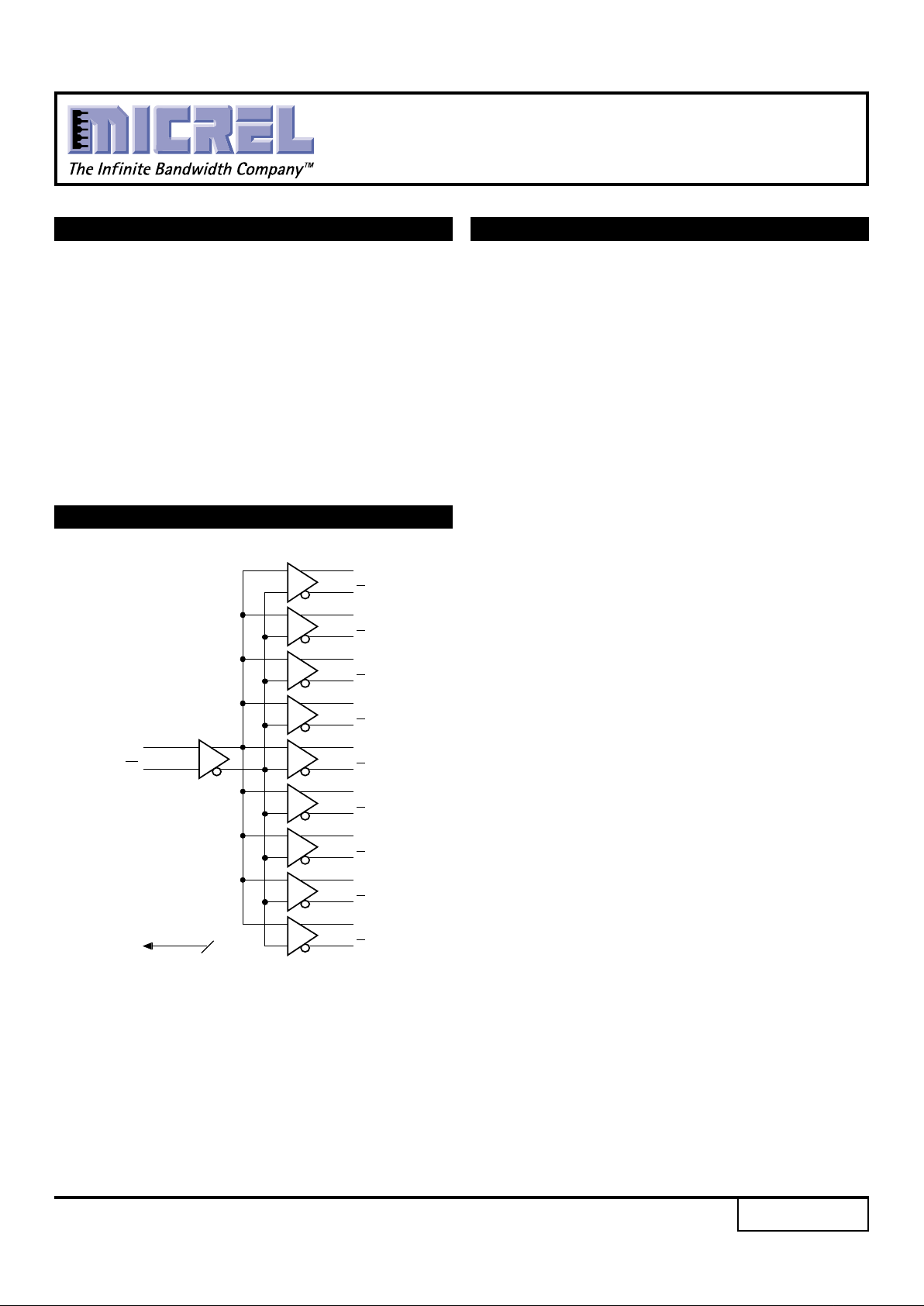
The SY10/100E111A/L are low skew 1-to-9 differential
driver designed for clock distribution in mind. The SY10/
100E111A/L's function and performance are similar to the
popular SY10/100E111, with the improvement of lower
jitter and the added feature of low voltage operation. It
accepts one signal input, which can be either differential or
single-ended if the VBB output is used. The signal is fanned
out to 9 identical differential outputs.
The E111A/L are specifically designed, modeled and
produced with low skew as the key goal. Optimal design
and layout serve to minimize gate to gate skew within a
device, and empirical modeling is used to determine process
control limits that ensure consistent tpd distributions from
lot to lot. The net result is a dependable, guaranteed low
skew device.
To ensure that the tight skew specification is met it is
necessary that both sides of the differential output are
terminated into 50Ω, even if only one side is being used. In
most applications, all nine differential pairs will be used and
therefore terminated. In the case where fewer that nine
pairs are used, it is necessary to terminate at least the
output pairs on the same package side as the pair(s) being
used on that side, in order to maintain minimum skew.
Failure to do this will result in small degradations of
propagation delay (on the order of 10-20ps) of the output(s)
being used which, while not being catastrophic to most
designs, will mean a loss of skew margin.
The E111A/L, as with most other ECL devices, can be
operated from a positive VCC supply in PECL mode. This
allows the E111A/L to be used for high performance clock
distribution in +5V/+3.3V systems. Designers can take
advantage of the E111A/L's performance to distribute low
skew clocks across the backplane or the board. In a PECL
environment, series or Thevenin line terminations are
typically used as they require no additional power supplies.
For systems incorporating GTL, parallel termination offers
the lowest power by taking advantage of the 1.2V supply as
terminating voltage.
BLOCK DIAGRAM
IN
V
BB
Q
0
Q
0
Q
1
Q
1
Q
2
Q
2
Q
3
Q
3
Q
4
Q
4
Q
5
Q
5
Q
6
Q
6
Q
7
Q
7
Q
8
Q
8
IN
1
Page 2
2
ClockWorks™
SY10E111A/L
SY100E111A/L
Micrel
T
A = –40°CTA = 0°CTA = +25°CTA = +85°C
Symbol Parameter Min. Typ. Max. Min. Typ. Max. Min. Typ. Max. Min. Typ. Max. Unit
V
OH Output HIGH Voltage mV
10EL –1080 — –890 –1020 — –840 –980 — –810 –910 — –720
100EL –1085 — –880 –1025 — –880 –1025 — –880 –1025 — –880
V
OL Output LOW Voltage mV
10EL –1950 — –1650 –1950 — –1630 –1950 — –1630 –1950 — –1595
100EL –1830 — –1550 –1810 — –1620 –1810 — –1620 –1810 — –1620
V
IH Input HIGH Voltage mV
10EL –1230 — –890 –1170 — –840 –1130 — –810 –1060 — –720
100EL –1165 — –880 –1165 — –880 –1165 — –880 –1165 — –880
V
IL Input LOW Voltage mV
10EL –1950 — –1500 –1950 — –1480 –1950 — –1480 –1950 — –1445
100EL –1810 — –1475 –1810 — –1475 –1810 — –1475 –1810 — –1475
V
BB Output Reference V
Voltage 10EL –1.43 — –1.30 –1.38 — –1.27 –1.35 — –1.25 –1.31 — –1.19
100EL –1.38 — –1.26 –1.38 — –1.26 –1.38 — –1.26 –1.38 — –1.26
IIH Input HIGH Current — — 150 — — 150 — — 150 — — 150 µA
I
IL Input LOW Current µA
10EL 0.5 — — 0.5 — — 0.5 — — 0.3 — —
100EL 0.5 — — 0.5 — — 0.5 — — 0.5 — —
I
EE Power Supply Current mA
10EL 35 — 65 35 — 65 35 — 65 35 — 65
100EL 35 — 65 35 — 65 35 — 65 35 — 75
VEE = VEE (Min.) to VEE (Max.); VCC = GND
NOTE:
1. Parametric values specified at: 5 volt Power Supply Range 100E111A Series: -4.2V to -5.5V.
10E111A Series -4.75V to -5.5V.
3 volt Power Supply Range 10/100E111L Series: -3.0V to -3.8V.
ECL DC ELECTRICAL CHARACTERISTICS
(1)
PIN CONFIGURATION
V
CC
V
EE
NC
V
BB
IN
Q
2
26
27
28
1
2
3
4
18
17
16
15
14
13
12
25 24 23 22 21 20 19
567891011
NC
IN
Q6Q
6
Q
3
Q
1
PLCC
TOP VIEW
J28-1
Q
2
Q0Q
0
V
CCO
Q
1
Q
3
Q
4
V
CCO
Q
4
Q
5
Q
5
Q
7
V
CCO
Q
7
Q
8
Q
8
PIN NAMES
Pin Function
IN, IN Differential Input Pair
Q0, Q0 — Q8, Q8 Differential Outputs
VBB VBB Output
V
CCO VCC to Output
Page 3

3
ClockWorks™
SY10E111A/L
SY100E111A/L
Micrel
3.3V PECL DC ELECTRICAL CHARACTERISTICS
(1)
VCC = +3.0V to +3.8V, VEE = GND
TA = –40°CTA = 0°CTA = +25°CTA = +85°C
Symbol Parameter Min. Typ. Max. Min. Typ. Max. Min. Typ. Max. Min. Typ. Max. Unit
VOH Output HIGH Voltage
(2)
mV
10EL 2220 — 2110 2280 — 2460 2320 — 2490 2390 — 2580
100EL 2215 — 2120 2275 — 2420 2275 — 2420 2275 — 2420
VOL Output LOW Voltage
(2)
mV
10EL 1350 — 1650 1350 — 1670 1350 — 1670 1350 — 1705
100EL 1470 — 1750 1490 — 1680 1490 — 1680 1490 — 1680
VIH Input HIGH Voltage
(2)
mV
10EL 2070 — 2410 2130 — 2460 2170 — 2490 2240 — 2580
100EL 2135 — 2420 2135 — 2420 2135 — 2420 2135 — 2420
VIL Input LOW Voltage
(2)
mV
10EL 1350 — 1800 1350 — 1820 1350 — 1820 1350 — 1855
100EL 1490 — 1825 1490 — 1825 1490 — 1825 1490 — 1825
VBB Output Reference V
Voltage
(2)
10EL 1.87 — 2.00 1.92 — 2.03 1.95 — 2.05 1.99 — 2.11
100EL 1.92 — 2.04 1.92 — 2.04 1.92 — 2.04 1.92 — 2.04
IIH Input HIGH Current ——150 ——150 ——150 ——150 µA
IIL Input LOW Current µA
10EL 0.5 ——0.5 ——0.5 —— 0.3 ——
100EL 0.5 ——0.5 ——0.5 —— 0.5 ——
IEE Power Supply Current mA
10EL ——66 ——66 ——66 ——66
100EL ——66 ——66 ——66 ——78
NOTES:
1. Parametric values specified at: 3 volt Power Supply Range 10/100E111L Series: +3.0V to +3.8V.
2. These values are for VCC = 3.3V. Level specifications will vary 1:1 with VCC.
5V PECL DC ELECTRICAL CHARACTERISTICS
(1)
VCC = VCC (Min.) to VCC (Max.); VEE = GND
TA = –40°CTA = 0°CTA = +25°CTA = +85°C
Symbol Parameter Min. Typ. Max. Min. Typ. Max. Min. Typ. Max. Min. Typ. Max. Unit
VOH Output HIGH Voltage
(2)
mV
10EL 3920 — 4110 3980 — 4160 4020 — 4190 4090 — 4280
100EL 3915 — 4120 3975 — 4120 3975 — 4120 3975 — 4120
V
OL Output LOW Voltage
(2)
mV
10EL 3050 — 3350 3050 — 3370 3050 — 3370 3050 — 3405
100EL 3170 — 3450 3190 — 3380 3190 — 3380 3190 — 3380
V
IH Input HIGH Voltage
(2)
mV
10EL 3770 — 4110 3830 — 4160 3870 — 4190 3940 — 4280
100EL 3835 — 4120 3835 — 4120 3835 — 4120 3835 — 4120
V
IL Input LOW Voltage
(2)
mV
10EL 3050 — 3500 3050 — 3520 3050 — 3520 3050 — 3555
100EL 3190 — 3525 3190 — 3525 3190 — 3525 3190 — 3525
V
BB Output Reference V
Voltage
(2)
10EL 3.57 — 3.70 3.62 — 3.73 3.65 — 3.75 3.69 — 3.81
100EL 3.62 — 3.74 3.62 — 3.74 3.62 — 3.74 3.62 — 3.74
IIH Input HIGH Current ——150 ——150 ——150 ——150 µA
I
IL Input LOW Current µA
10EL 0.5 ——0.5 ——0.5 —— 0.3 ——
100EL 0.5 ——0.5 ——0.5 —— 0.5 ——
I
EE Power Supply Current mA
10EL ——66 ——66 ——66 ——66
100EL ——66 ——66 ——66 ——78
NOTES:
1. Parametric values specified at: 5 volt Power Supply Range 100E111A Series: +4.2V to +5.5V.
10E111A Series +4.75V to +5.5V.
2. These values are for VCC = 5V. Level specifications will vary 1:1 with VCC.
Page 4

4
ClockWorks™
SY10E111A/L
SY100E111A/L
Micrel
VEE = VEE (Min.) to VEE (Max.); VCC = GND
TA = -40°CTA = 0°CTA = +25°CTA = +85°C
Symbol Parameter Min. Typ. Max. Min. Typ. Max. Min. Typ. Max. Min. Typ. Max. Unit
t
PLH Propagation Delay to Output ps
tPHL IN (differential)
(2)
380 — 680 430 — 630 430 — 630 430 — 630
IN (single-ended)
(3)
280 — 780 330 — 730 330 — 730 330 — 730
t
skew Within-Device Skew
(4)
——75 ——50 ——50 ——50 ps
Part-to-Part Skew (Diff.) ——250 ——200 ——200 ——200
VPP Minimum Input Swing
(5)
250 ——250 ——250 ——250 ——mV
VCMR Common Mode Range
(6)
–1.5 —–0.4 –1.5 —–0.4 –1.5 —–0.4 –1.5 —–0.4 V
tr Rise/Fall Times 200 — 650 200 — 600 200 — 600 200 — 600 ps
tf 20% to 80%
AC ELECTRICAL CHARACTERISTICS
NOTES:
1. Parametric values specified at: 5 volt Power Supply Range 100E111A Series: -4.2V to -5.5V.
10E111A Series -4.75V to -5.5V.
3 volt Power Supply Range 10/100E111L Series: -3.0V to -3.8V.
2. The differential propagation delay is defined as the delay from the crossing points of the differential input signals to the crossing point of the
differential output signals.
3. The single-ended propagation delay is defined as the delay from the 50% point of the input signal to the 50% point of the output signal.
4. The within-device skew is defined as the worst case difference between any two similar delay paths within a single device.
5. VPP (min) is defined as the minimum input differential voltage which will cause no increase in the propagation delay. The VPP (min) is AC limited for
the E111A/L as a differential input as low as 50mV will still produce full ECL levels at the output.
6. VCMR is defined as the range within the VIH level may vary, with the device still meeting the propagation delay specification. The VIL level must be
such that the peak-to-peak voltage is less than 1.0V and greater than or equal to VPP (min).
For PECL operation: VCMR (max) = VCC – |VCMR (max)| and
VCMR (min) = VCC – |VCMR (min)|
Ordering Package Operating VEE Range
Code Type Range (V)
SY10E111AJC J28-1 Commercial -4.75 to -5.5
SY10E111AJCTR J28-1 Commercial -4.75 to -5.5
SY100E111AJC J28-1 Commercial -4.2 to -5.5
SY100E111AJCTR J28-1 Commercial -4.2 to -5.5
PRODUCT ORDERING CODE
SY10E111LJC J28-1 Commercial -3.0 to -3.8
SY10E111LJCTR J28-1 Commercial -3.0 to -3.8
SY100E111LJC J28-1 Commercial -3.0 to -3.8
SY100E111LJCTR J28-1 Commercial -3.0 to -3.8
5V
3.3V
Ordering Package Operating VEE Range
Code Type Range (V)
SY10E111AJI J28-1 Industrial -4.75 to -5.5
SY10E111AJITR J28-1 Industrial -4.75 to -5.5
SY100E111AJI J28-1 Industrial -4.2 to -5.5
SY100E111AJITR J28-1 Industrial -4.2 to -5.5
SY10E111LJI J28-1 Industrial -3.0 to -3.8
SY10E111LJITR J28-1 Industrial -3.0 to -3.8
SY100E111LJI J28-1 Industrial -3.0 to -3.8
SY100E111LJITR J28-1 Industrial -3.0 to -3.8
5V
3.3V
Page 5

5
ClockWorks™
SY10E111A/L
SY100E111A/L
Micrel
28 LEAD PLCC (J28-1)
Rev. 03
MICREL-SYNERGY 3250 SCOTT BOULEVARD SANTA CLARA CA 95054 USA
TEL + 1 (408) 980-9191 FAX + 1 (408) 914-7878 WEB http://www.micrel.com
This information is believed to be accurate and reliable, however no responsibility is assumed by Micrel for its use nor for any infringement of patents or
other rights of third parties resulting from its use. No license is granted by implication or otherwise under any patent or patent right of Micrel Inc.
© 2000 Micrel Incorporated
 Loading...