

Page 1
®
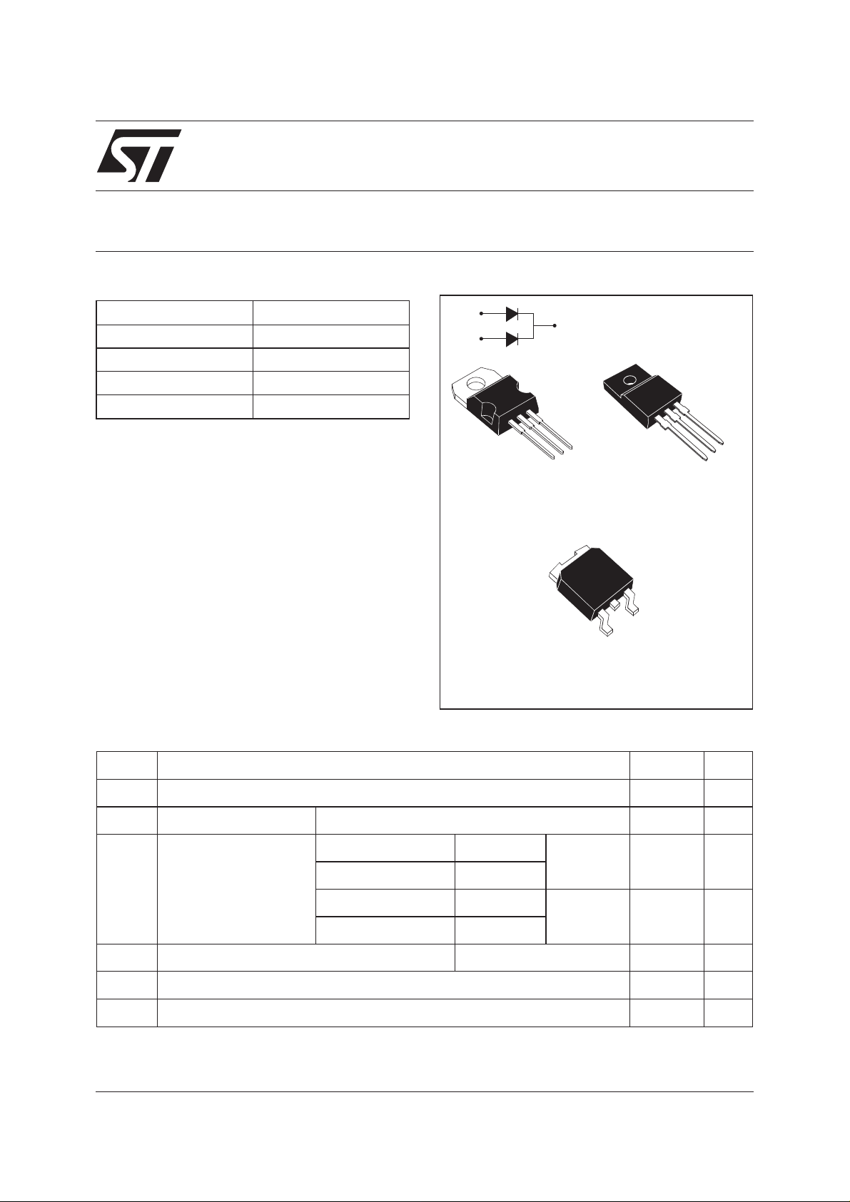
HIGH EFFICIENCY ULTRAFAST DIODE
MAIN PRODUCT CHARACTERISTICS
I
F(AV)
V
RRM
Tj (max) 175 °C
(max) 0.95 V
V
F
trr (max) 20 ns
2x4A
200 V
STTH802CT/CB/CFP
A1
K
A2
FEATURES AND BENEFITS
Suited for SMPS
■
Low losses
■
Low forward and reverserecovery times
■
High surge current capability
■
■ High junction temperature
■ Insulated package: TO-220FPAB
TO-220AB
STTH802CT
A1
A2
K
A1
K
TO-220FPAB
STTH802CFP
K
DESCRIPTION
Dual center tap rectifier suited for Switch Mode
Power Supplies and High frequency DC to DC
converters.
Packaged in DPAK, TO-220AB or TO-220FPAB.
This device is intended foruseinlow voltage, high
frequency inverters, free wheeling and polarity
DPAK
STTH802CB
A1
A2
K
protection applications.
ABSOLUTE RATINGS (limiting values)
Symbol Parameter Value Unit
V
RRM
I
F(RMS)
I
F(AV)
Repetitive peak reverse voltage 200 V
RMS forward current TO-220AB / TO-220FPAB /DPAK 10 A
Average forward
current δ =0.5
TO-220AB / DPAK Tc = 155°C Per diode 4 A
TO-220FPAB Tc = 145°C
A2
TO-220AB / DPAK Tc = 150°C Per device 8 A
TO-220FPAB Tc = 130°C
I
FSM
T
stg
Surge non repetitive forwardcurrent tp = 10 ms Sinusoidal 50 A
Storage temperature range - 65 + 175 °C
Tj Maximum operating junction temperature 175 °C
April 2002 - Ed: 1A
1/8
Page 2

STTH802/CT/CB/CFP
THERMAL PARAMETERS
Symbol Parameter Maximum Unit
R
th (j-c)
Junction to case TO-220AB / DPAK Per diode 4.0 °C/W
TO-220FPAB 6.5
TO-220AB / DPAK Total 2.5
TO-220FPAB 5
R
th (j-c)
Coupling TO-220AB / DPAK 1 °C/W
TO-220FPAB 3.5
When the diodes 1 and 2 are used simultaneously:
∆ Tj (diode1) = P(diode1) x R
(per diode) + P(diode2) x R
th(j-c)
th(c)
STATIC ELECTRICAL CHARACTERISTICS
Symbol Parameter Tests conditions Min. Typ. Max. Unit
I
* Reverse leakage
R
current
V
** Forward voltage drop Tj = 25°C I
F
Tj = 25°C V
R=VRRM
4 µA
Tj = 125°C 2 40
= 4 A 1.1 V
F
Tj = 125°C I
Tj = 25°C I
= 4 A 0.81 0.95
F
= 8 A 1.25
F
Tj = 125°C I
Pulse test: * tp = 5ms, δ <2%
** tp = 380µs, δ <2%
= 8 A 0.95 1.1
F
To evaluate the maximumconduction losses use the following equation :
P=0.80xI
F(AV)
+ 0.037 I
F2(RMS)
DYNAMIC ELECTRICAL CHARACTERISTICS
Symbol Parameter Tests conditions Min. Typ. Max. Unit
trr Reverse recovery
time
tfr Forward recovery
time
V
FP
Forward recovery
Tj = 25°C I
Tj = 25°C I
Tj = 25°C I
= 0.5 A Irr = 0.25 A
F
IR=1A
=4A dIF/dt = 100 A/µs
F
VFR=1.1xVFmax
=4A dIF/dt = 100 A/µs 2.4 V
F
13 20 ns
50 ns
voltage
2/8
Page 3
STTH802/CT/CB/CFP
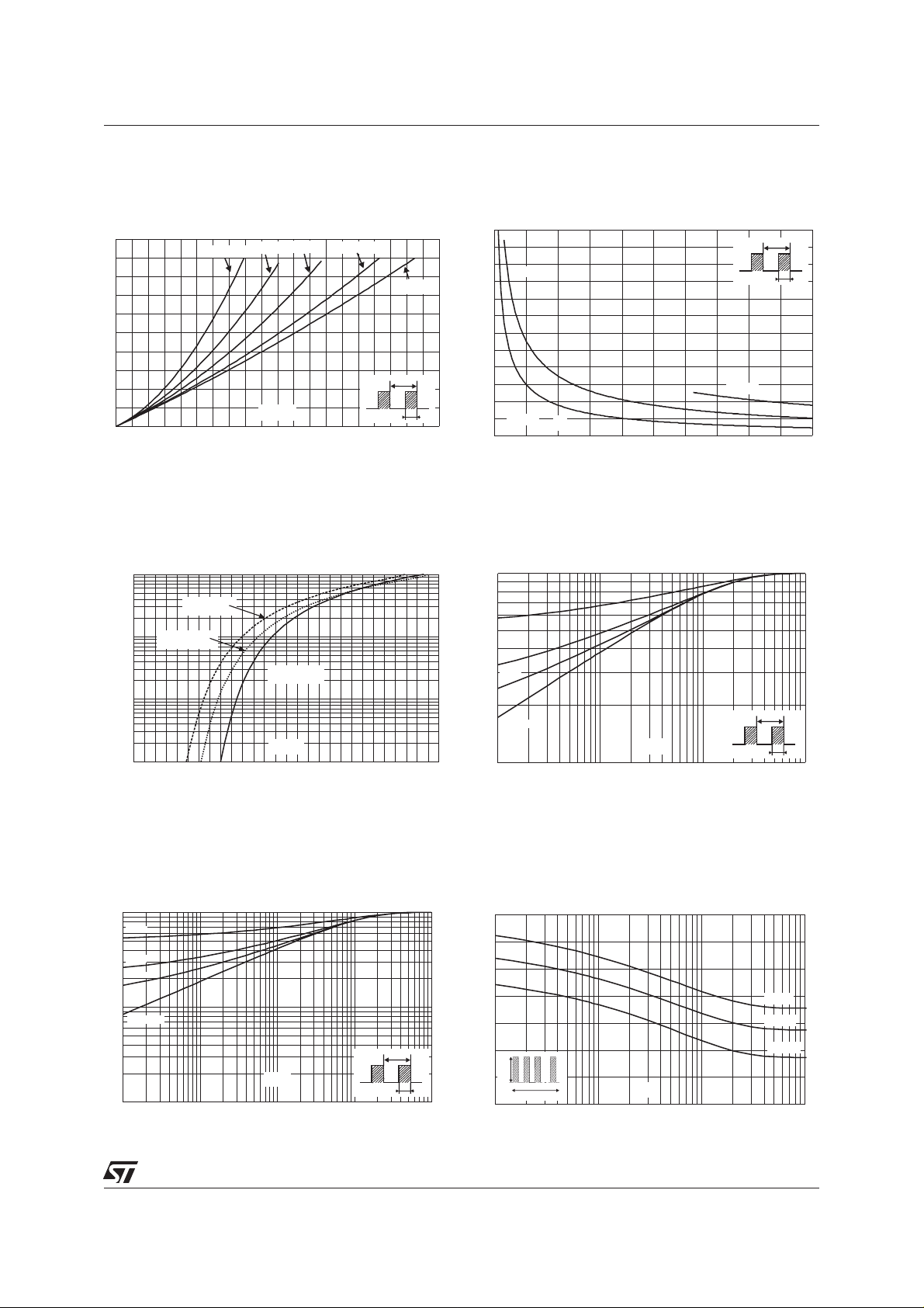
Fig. 1: Average forward power dissipation versus
average forward current (per diode).
P (W)F(av)
5
4
3
2
1
0
0.0 0.5 1.0 1.5 2.0 2.5 3.0 3.5 4.0 4.5 5.0
δ = 0.05
δ = 0.1
I (A)F(av)
δ = 0.2
δ = 0.5
δ
=tp/T
δ = 1
T
tp
Fig. 3: Forward voltage drop versus forward
current (per diode).
I (A)FM
100.0
Tj=125°C
Tj=125°C
Typical values
Typical values
Tj=125°C
10.0
1.0
0.1
0.0 0.2 0.4 0.6 0.8 1.0 1.2 1.4 1.6 1.8 2.0 2.2 2.4 2.6 2.8
Tj=125°C
Maximum values
Maximum values
Tj=25°C
Maximum values
V (V)FM
Fig.2:Peak current versusformfactor (per diode).
I (A)M
60
50
P= 5W
40
30
20
10
P= 2W
0
0.0 0.1 0.2 0.3 0.4 0.5 0.6 0.7 0.8 0.9 1.0
δ
δ
P = 10W
=tp/T
T
tp
Fig. 4-1: Relative variation of thermal impedance
junctiontocaseversuspulseduration(TO-220AB,
DPAK).
Zth(j-c) / Rth(j-c)
1.0
δ = 0.5
δ = 0.2
δ = 0.1
δ
=tp/T
T
tp
Single pulse
tp(s)
0.1
1.E-03 1.E-02 1.E-01 1.E+00
Fig. 4-2:Relativevariation of thermal impedance
junctiontocase versus duration(TO-220FPAB).
Zth(j-c) / Rth(j-c)
1.0
δ = 0.5
δ = 0.2
δ = 0.1
0.1
Single pulse
T
tp(s)
=tp/T
0.0
1.E-03 1.E-02 1.E-01 1.E+00 1.E+01
δ
tp
Fig. 5-1: Non repetitive surge peak forward
current versus overload duration per diode
(TO-220AB, DPAK).
I (A)M
70
60
50
40
30
20
IM
10
0
1.E-03 1.E-02 1.E-01 1.E+00
δ=0.5
t
t(s)
Tc=25°C
Tc=75°C
Tc=125°C
3/8
Page 4

STTH802/CT/CB/CFP
Fig. 5-2: Non repetitive surge peak forward
current versus overload duration per diode
(TO-220FPAB).
I (A)M
60
50
40
30
20
IM
10
0
1.E-03 1.E-02 1.E-01 1.E+00
δ=0.5
t
t(s)
Tc=25°C
Tc=75°C
Tc=125°C
Fig. 7: Junction capacitance versus reverse
voltage applied (typical values, per diode).
C(pF)
100
F=1MHz
Vosc=30mV
Tj=25°C
RMS
Fig. 6:Averageforwardcurrent versus ambient
temperature (δ = 0.5, per diode).
I )(A)F(av
5.0
4.5
4.0
3.5
3.0
2.5
2.0
1.5
DPAK (S=0.5cm²)
1.0
0.5
0.0
Rth(j-a)=70°C:W
0 25 50 75 100 125 150 175
Rth(j-a)=Rth(j-c)
Tamb(°C)
TO-220AB/DPAK
TO-220FPAB
Fig. 8: Reverse recovery charges versus dIF/dt
(90% confidence, per diode).
Q (nC)RR
1000
IF=4A
VR=200V
Tj=125°C
VR(V)
10
1 10 100 1000
Fig. 9: Peak reverse recovery current versus
dIF/dt (90% confidence, per diode).
I (A)RM
100.0
IF=4A
VR=200V
Tj=125°C
10.0
1.0
dI /dt(A/µs)F
0.1
10 100 1000
100
dIF/dt(A/µs)
10
10 100 1000
Fig. 10: Dynamic parameters versus junction
temperature.
Q ;I [Tj] / Q ; I [Tj = 125°C]RR RM RR RM
1.4
IF=4A
=200V
V
R
1.2
1.0
0.8
0.6
0.4
0.2
0.0
0 25 50 75 100 125 150
I
RM
Q
RR
Tj(°C)
4/8
Page 5

Fig. 11: Thermal resistance junction to ambient
versus copper surface under tab (Epoxy printed
circuit board FR4, copper thickness: 35µm) for
DPAK.
(j-a)
Rth (°CW)
100
90
80
70
60
50
40
30
20
10
0
0 2 4 6 8 101214161820
S(cm²)
PACKAGE MECHANICAL DATA
TO-220AB
STTH802CT/CB/CFP
L2
F1
F2
F
G1
H2
Dia
DIMENSIONS
REF.
Millimeters Inches
Min. Max. Min. Max.
A 4.40 4.60 0.173 0.181
A
C
C 1.23 1.32 0.048 0.051
D 2.40 2.72 0.094 0.107
E 0.49 0.70 0.019 0.027
L5
L7
L6
F 0.61 0.88 0.024 0.034
F1 1.14 1.70 0.044 0.066
F2 1.14 1.70 0.044 0.066
G 4.95 5.15 0.194 0.202
L9
D
L4
G1 2.40 2.70 0.094 0.106
H2 10 10.40 0.393 0.409
L2 16.4 typ. 0.645 typ.
M
E
G
L4 13 14 0.511 0.551
L5 2.65 2.95 0.104 0.116
L6 15.25 15.75 0.600 0.620
L7 6.20 6.60 0.244 0.259
L9 3.50 3.93 0.137 0.154
M 2.6 typ. 0.102 typ.
Diam. 3.75 3.85 0.147 0.151
5/8
Page 6

STTH802CT/CB/CFP
PACKAGE MECHANICAL DATA
DPAK
DIMENSIONS
REF.
Millimeters Inches
Min. Max Min. Max.
A 2.20 2.40 0.086 0.094
A1 0.90 1.10 0.035 0.043
A2 0.03 0.23 0.001 0.009
B 0.64 0.90 0.025 0.035
B2 5.20 5.40 0.204 0.212
C 0.45 0.60 0.017 0.023
C2 0.48 0.60 0.018 0.023
D 6.00 6.20 0.236 0.244
E 6.40 6.60 0.251 0.259
G 4.40 4.60 0.173 0.181
H 9.35 10.10 0.368 0.397
L2 0.80 typ. 0.031 typ.
L4 0.60 1.00 0.023 0.039
V2 0° 8° 0° 8°
FOOTPRINT
6.7
6.7
3
3
1.61.6
2.32.3
6/8
Page 7

PACKAGE MECHANICAL DATA
TO-220FPAB
H
Dia
L6
L2
L3
L5
D
L4
G1
F1
F2
F
STTH802/CT/CB/CFP
DIMENSIONS
REF.
A 4.4 4.6 0.173 0.181
A
B
B 2.5 2.7 0.098 0.106
D 2.5 2.75 0.098 0.108
E 0.45 0.70 0.018 0.027
F 0.75 1 0.030 0.039
F1 1.15 1.70 0.045 0.067
L7
F2 1.15 1.70 0.045 0.067
G 4.95 5.20 0.195 0.205
G1 2.4 2.7 0.094 0.106
H 10 10.4 0.393 0.409
L2 16 Typ. 0.63 Typ.
L3 28.6 30.6 1.126 1.205
L4 9.8 10.6 0.386 0.417
E
L5 2.9 3.6 0.114 0.142
Millimeters Inches
Min. Max. Min. Max.
G
L6 15.9 16.4 0.626 0.646
L7 9.00 9.30 0.354 0.366
Dia. 3.00 3.20 0.118 0.126
Ordering code Marking Package Weight Base qty Delivery mode
STTH802CT STTH802CT TO-220AB 2.23 g 50 Tube
STTH802CB STTH802CB DPAK 0.3 g 75 Tube
STTH802CB-TR STTH802CB DPAK 0.3 g 2500 Tape & reel
STTH802CFP STTH802CFP TO-220FPAB 2.0 g 50 Tube
■
Cooling method: by conduction (method C)
■
Recommended torque value (TO-220AB): 0.8 N.m
■
Maximum torque value (TO-220AB): 1.0 N.m
■
Recommended torque value (TO-220FPAB): 0.55 N.m
■
Maximum torque value (TO-220FPAB): 0.7 N.m
■
Epoxy meets UL 94,V0
7/8
Page 8

STTH802CT/CB/CFP
Informationfurnished isbelievedto beaccurate and reliable.However, STMicroelectronics assumesno responsibilityforthe consequencesof
useof suchinformation nor forany infringementof patents orother rights ofthird partieswhich may resultfrom itsuse. No licenseis granted by
implication or otherwise under any patent or patent rights of STMicroelectronics. Specifications mentioned in this publication are subject to
change withoutnotice. This publication supersedes and replaces allinformation previously supplied.
STMicroelectronics products are not authorized for use as critical components in life support devices or systems without express written approval ofSTMicroelectronics.
The ST logo is a registered trademark of STMicroelectronics
© 2002 STMicroelectronics - Printed in Italy - All rights reserved.
STMicroelectronics GROUP OF COMPANIES
Australia - Brazil - Canada - China - Finland - France - Germany
Hong Kong - India - Israel - Italy - Japan - Malaysia - Malta - Morocco - Singapore
Spain - Sweden - Switzerland - United Kingdom - United States.
http://www.st.com
8/8
 Loading...