

Page 1
MICROWAVE CORPORATION
LOW NOISE AMPLIFIER 5.0 - 6.0 GHz
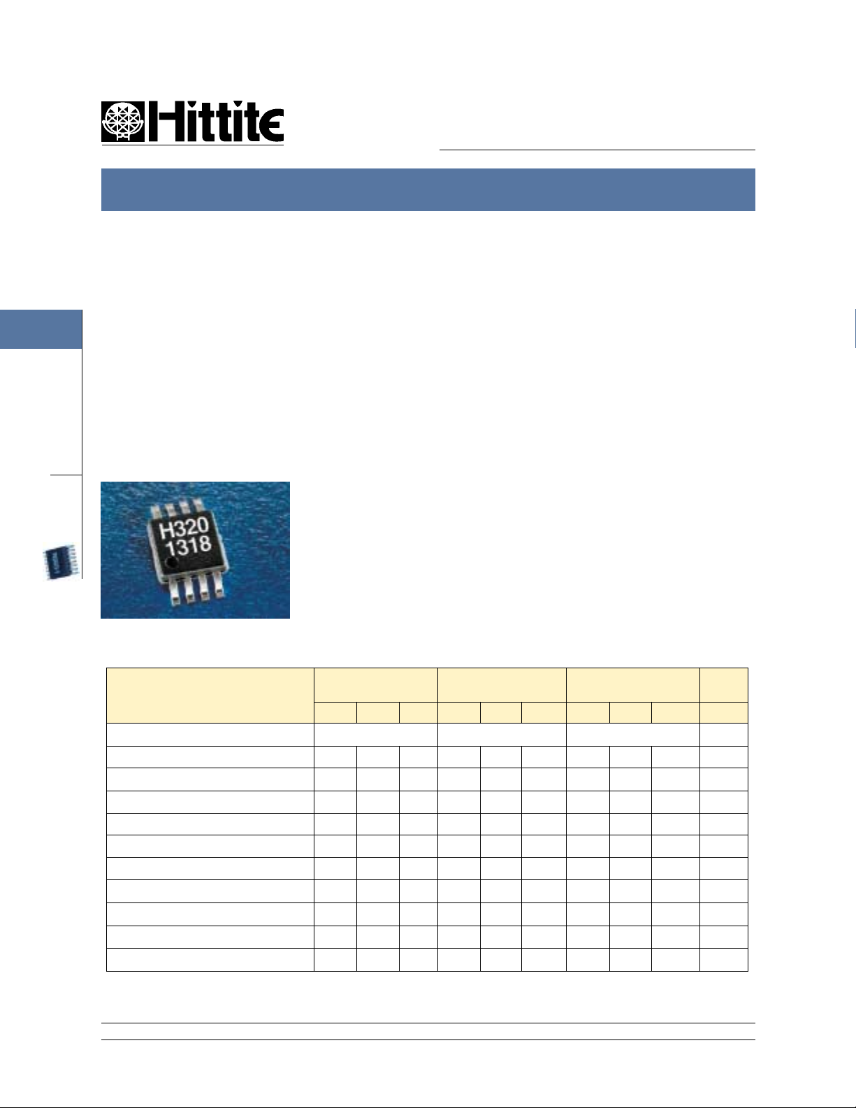
HMC320MS8G
FEBRUARY 2001
Features
Selectable Functionality:
LNA, Driver, or LO Buffer Amp
1
Adjustable Input IP3
Up To +10 dBm
+3V Operation
Ultra Small 8 Lead MSOP:
AMPLIFIERS
14.8 mm² x 1mm High
SMT
V00.0900
General Description
The HMC320MS8G is a low cost C-band fixed
gain Low Noise Amplifier (LNA) that serves the
full UNII and HiperLAN bands. The
HMC320MS8G operates using a single positive
supply that can be set between +3V and +5V.
With +3V bias, the LNA provides a noise figure
of 2.5 dB, 12 dB gain and better than 10 dB return
loss across the UNII band. The HMC320MS8G
also features adaptive biasing that allows the
user to select the optimal P1dB performance for
their system using an external set resistor on the
“RES” pin. P1dB performance can be set between a range of +1 dBm to +13 dBm. The low
cost LNA uses an 8-leaded MSOP ground base
surface mount plastic package, which occupies
less than 14.8mm
2
.
Guaranteed Performance,
retemaraP
egnaRycneuqerF6-56-56-5zHG
C°52@niaG801618 216193161Bd
pmeTrevonoitairaVniaG520.0530.0520.0530.0520.0530.0/BdC°
ssentalFniaG5.0±0.1±5.1±Bd
erugiFesioN7.28.35.28.36.28.3Bd
ssoLnruteRtupnI401401401Bd
ssoLnruteRtuptuO73101810102Bd
)Bd1P(tnioPnoisserpmoCBd1tuptuO4-1-69921mBd
)3PII(tnioPtpecretnIredrOdrihTtupnI3-1 48 601mBd
)ddV(egatloVylppuSdednemmoceR57.20.352.357.20.352.357.20.352.3cdV
)ddI(tnerruCylppuS75204Am
* RBIAS resistor value sets current. See adaptive biasing application note.
12 Elizabeth Drive, Chelmsford, MA 01824 Phone: 978-250-3343 Fax: 978-250-3373 Web Site: www.hittite.com
Vdd = +3V, -40 to +85 deg C
*rewoPwoL
)Am7=ddI,V0=TESV(
.niM .pyT .xaM .niM .pyT .xaM .niM .pyT .xaM stinU
*rewoPmuideM
)Am52=ddI,V3=TESV(
*rewoPhgiH
)Am04=ddI,V3=TESV(
1 - 144
Page 2
MICROWAVE CORPORATION
LOW NOISE AMPLIFIER 5.0 - 6.0 GHz
HMC320MS8G
V00.0900
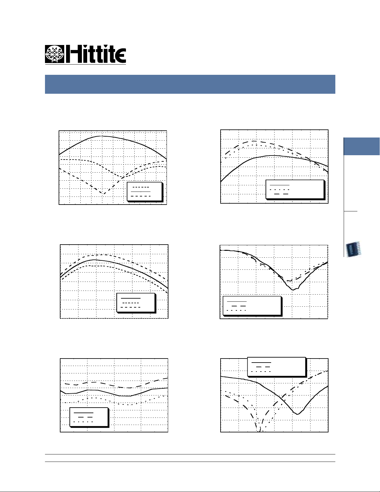
Broadband Gain & Return Loss
Medium Power Bias
15
10
5
0
-5
-10
-15
RESPONSE (dB)
-20
-25
-30
33.544.555.566.577.58
FREQUENCY (GHz)
Gain vs. Temperature
Medium Power Bias
16
14
12
10
8
GAIN (dB)
6
4
2
0
44.555.566.57
FREQUENCY (GHz)
+25 C
+85 C
-40 C
Noise Figure vs. Temperature
Medium Power Bias
5
4.5
4
3.5
3
2.5
2
1.5
NOISEFIGURE(dB)
1
0.5
0
4.5 5 5.5 6 6.5
+25 C
+85 C
-40 C
FREQUENCY (GHz)
S11
S21
S22
FEBRUARY 2001
Gain @ Three Bias Conditions
16
14
12
10
8
GAIN (dB)
6
4
2
0
4 4.5 5 5.5 6 6.5 7
FREQU E NCY (GHz)
Low Power Bias
Medium Power Bias
High Power Bias
Input Return Loss
@ Three Bias Conditions
0
-5
-10
-15
-20
INPUT R ETUR N LOS S (dB)
-25
-30
4 4.5 5 5.5 6 6.5 7
Low Power Bias
Medium PowerBias
High PowerBias
FREQU E NCY (GHz)
Output Return Loss
@Three Bias Conditions
0
-5
-10
-15
-20
OUTPUT RETURN LOSS (dB)
-25
-30
4 4.5 5 5.5 6 6.5 7
Low Power Bias
Medium Power Bias
High Power Bias
FREQU E NCY (GHz)
1
AMPLIFIERS
SMT
12 Elizabeth Drive, Chelmsford, MA 01824 Phone: 978-250-3343 Fax: 978-250-3373 Web Site: www.hittite.com
1 - 145
Page 3

MICROWAVE CORPORATION
LOW NOISE AMPLIFIER 5.0 - 6.0 GHz
HMC320MS8G
FEBRUARY 2001
Noise Figure
@ Three Bias Conditions
1
NOISE FIGURE (dB)
AMPLIFIERS
Output 1dB Compression
SMT
@ Three Bias Conditions
P1dB (dBm)
5
4.5
4
3.5
3
2.5
2
1.5
1
0.5
0
4.5 5 5.5 6 6.5
15
13
11
9
7
5
3
1
-1
-3
-5
4.5 5 5.5 6 6.5
Low Power Bias
Medium PowerBias
High Power Bias
FREQU E NCY (GHz)
Low Power Bias
Medium Power Bias
High Power Bias
FREQU E NCY (GHz)
V00.0900
Input IP3 @Three Bias Conditions
15
13
11
9
7
5
3
INPUT IP3 (dBm)
1
-1
-3
-5
4.5 5 5.5 6 6.5
Low Power Bias
Medium PowerBias
High PowerBias
FREQU E NCY (GHz)
Reverse Isolation
@ Three Bias Conditions
0
-10
-20
-30
-40
REVERSE ISOLATION (dB)
-50
-60
4 4.5 5 5.5 6 6.5 7
Low Power Bias
Medium PowerBias
High Power Bias
FREQU E NCY (GHz)
12 Elizabeth Drive, Chelmsford, MA 01824 Phone: 978-250-3343 Fax: 978-250-3373 Web Site: www.hittite.com
1 - 146
Page 4

MICROWAVE CORPORATION
LOW NOISE AMPLIFIER 5.0 - 6.0 GHz
HMC320MS8G
V00.09.00
FEBRUARY 2001
Adaptive Biasing
Optimizing P1dB Performance of the HMC320MS8G
The bias level may be changed to adjust the P1dB and return loss performance. The table below contains
the HMC320MS8G RF performance as a function of various VSET and RBIAS settings. It will be necessary
for the VSET voltage source to provide 100uA of current to the amplifier. The Idd and Vdd quiescent
performance will not change as a function of changing the VSET voltage.
RF Performance at 5.8GHz (Vdd = +3v)
TESV
)CDV(
047170.10.61
332520.90.21
37 040.310.51
3
R SAIB rotsiseR
dna3niPneewteB
)smhO(DNG
DNG
)rotsiseRoN(
)Am(ddI
060.410.51
tuptuO
)mBd(Bd1P
tuptuO
ssoLnruteR
)Bd(
1
AMPLIFIERS
SMT
Applying the adaptive biasing
A dynamically controlled bias can be implemented with this design. A typical application will include
sensing an RF signal level and then adjusting the VSET. The bias adjustment can be accomplished by
either analog or digitals means, after the RF signal has been detected and translated to a DC voltage using
external power detection circuitry.
12 Elizabeth Drive, Chelmsford, MA 01824 Phone: 978-250-3343 Fax: 978-250-3373 Web Site: www.hittite.com
1 - 147
Page 5

MICROWAVE CORPORATION
HMC320MS8G
LOW NOISE AMPLIFIER 5 - 6 GHz
FEBRUARY 2001
Schematic
1
IN
(Pin 1)
AMPLIFIERS
Note: Internal DC blocks on
SMT
RF I/O's are included on HMC320MS8G
Outline
VSET
(Pin 8)
GND
(Pins 2, 4, 6)
Vdd
(Pin 7)
RES (Pin 3)
RBIAS
OUT
(Pin 5)
V00.0900
Absolute Maximum Ratings
)ddV(egatloVylppuScdV7+
TESVddVotV0
rewoPtupnImBd5+
)cT(erutarepmeTlennahCC°571
)C°58=aT(ssidPsuounitnoC
)C°58evobaC°/Wm89.2etared(
erutarepmeTegarotSC°051+ot56-
erutarepmeTgnitarepOC°58+ot55-
Wm862
T ruth Table
TESV
V0Am7rewoPwoLmhO471
V3Am52rewoPmuideMmhO32
V3Am04rewoPhgiHmhO7
Set external bias resister (R
operating current 0.0< R
gnitarepO
ddItnerruC
BIAS
BIAS
< 200
gnitarepO
etatS
) to achieve desired
Ω.
RretsiseR
SAIB
1. MATERIAL:
A) PACKAGE BODY - LOW STRESS INJECTION-MOLDED PLASTIC,
SILICA & SILICONE IMPREGNATED.
B) LEADFRAME MATERIAL: COPPER ALLOY
2 . PLATING : LEAD - TIN SOLDER PLATE
3. DIMENSIONS ARE IN INCHES (MILLIMETERS).
UNLESS OTHERWISE SPECIFIED ALL TOL. ARE ±0.005 (±0.13).
4. CHARACTERS TO BE HELVETICA MEDIUM, APPROX .020 HIGH
WHITE INK, LOCATED APPROXIMATELY AS SHOWN.
5. DIMENSION DOES NOT INCLUDE MOLDFLASH OF 0.15 MM PER SIDE
6. DIMENSION DOES NOT INCLUDE MOLDFLASH OF 0.25 MM PER SIDE
12 Elizabeth Drive, Chelmsford, MA 01824 Phone: 978-250-3343 Fax: 978-250-3373 Web Site: www.hittite.com
1 - 148
Page 6

MICROWAVE CORPORATION
HMC320MS8G
LOW NOISE AMPLIFIER 5 - 6 GHz
V00.0900
Evaluation PCB for HMC320MS8G
FEBRUARY 2001
1
AMPLIFIERS
SMT
The circuit board used in the final application should use RF circuit design techniques. Signal lines should have
50 ohm impedance while the package ground leads and exposed paddle should be connected directly to the
ground plane similar to that shown above. A sufficient number of VIA holes should be used to connect the top
and bottom ground planes. The evaluation circuit board as shown is available from Hittite upon request.
Evaluation Circuit Board Layout Design Details
metI noitpircseD
2J,1JrotcennoCAMStnuoMCP
4J,3JniPCD
1RretemoitnetoPmhO002
1UreifilpmAG8SM023CMH
*BCP"5.1x"6.1BCPnoitaulavE
0534sregoR:lairetaMdraoBtiucriC*
12 Elizabeth Drive, Chelmsford, MA 01824 Phone: 978-250-3343 Fax: 978-250-3373 Web Site: www.hittite.com
1 - 149
 Loading...