

Page 1
MICROWAVE CORPORATION
HBT BROADBAND AMPLIFIER GAIN BLOCK DC - 6.0 GHz
HMC313
FEBRUARY 2001
Features
P1dB Output Power: +19 dBm
1
Output IP3: +33 dBm
Single Supply: +5V to +7V
High Reliability GaAs HBT Process
AMPLIFIERS
Ultra Small SOT26 Package
SMT
V00.1100
General Description
The HMC313 is a GaAs InGaP Heterojunction
Bipolar Transistor (HBT) MMIC amplifier that
operates from a single Vcc supply. The surface
mount SOT26 amplifier can be used as a broadband gain stage or used with external matching
for optimized narrow band applications. With
Vcc biased at +7V, the HMC313 offers 18 dB of
gain and +20 dBm of saturated power while only
requiring 85 mA of current. The "HMC313 Biasing and Impedance Matching Techniques" application note on page 8-40 offers recommendations for narrow band operation. This amplifier is
ideal as a driver and amplifier for 2.2 - 2.7 GHz
MMDS, 3.5 GHz Wireless Local Loop Applications (WLL), 5.0 - 6.0 GHz UNII and HiperLAN
applications.
Guaranteed Performance, As a Function of Vcc, -40 to +65 deg C
retemaraP
.niM .pyT .xaM .niM .pyT .xaM
egnaRycneuqerF6-CD6-CDzHG
C°52@niaG 317102418112Bd
erutarepmeTrevonoitairaVniaG20.030.020.030.0/BdC°
ssoLnruteRtupnI3737Bd
ssoLnruteRtuptuO2626Bd
noitalosIesreveR62036203Bd
zHG0.1@)Bd1P(noisserpmoCBd1rofrewoPtuptuO11416191mBd
zHG0.1@)tasP(rewoPtuptuOdetarutaS21517102mBd
zHG0.1@)3PI(tpecretnIredrOdrihTtuptuO42720333mBd
erugiFesioN5.652.7Bd
)ccI(tnerruCylppuS0558Am
12 Elizabeth Drive, Chelmsford, MA 01824 Phone: 978-250-3343 Fax: 978-250-3373 Web Site: www.hittite.com
1 - 120
V5+=ccV V7+=ccV
stinU
Page 2
MICROWAVE CORPORATION
HBT BROADBAND AMPLIFIER GAIN BLOCK DC - 6.0 GHz
HMC313
V00.1100
Gain & Return Loss @ Vcc= +7V
25
20
15
10
5
0
-5
RESPONSE (dB)
-10
-15
-20
01234567
S11
S21
S22
FREQUENCY (GHz)
Gain & Return Loss @ Vcc= +5V
25
20
15
10
5
0
-5
RESPONSE (dB)
-10
-15
-20
01234567
S11
S21
S22
FREQUENCY (GHz)
FEBRUARY 2001
Gain vs. Temperature @ Vcc= +7V Gain vs. Temperature @ Vcc= +5V
25
20
15
25
20
15
1
AMPLIFIERS
SMT
+25C
GAIN (dB)
10
5
0
01234567
+85C
-40C
FREQUENCY (GHz)
Input & Output Return Loss vs. Vcc Bias
0
-5
-10
S11 @ Vcc=+5V
RETURN LOSS (dB)
-15
-20
01234567
S22 @ Vcc=+5V
S11 @ Vcc=+7V
S22 @ Vcc=+7V
FREQUENCY (GHz)
GAIN (dB)
10
5
0
01234567
Reverse Isolation vs. Vcc Bias
0
-10
-20
-30
ISOL A T IO N (dB )
-40
-50
01234567
+25C
+85C
-40C
FREQUENCY (GHz)
FREQUENCY (GHz)
+5V
+7V
12 Elizabeth Drive, Chelmsford, MA 01824 Phone: 978-250-3343 Fax: 978-250-3373 Web Site: www.hittite.com
1 - 121
Page 3
MICROWAVE CORPORATION
HBT BROADBAND AMPLIFIER GAIN BLOCK DC - 6.0 GHz
HMC313
FEBRUARY 2001
P1dB vs. Temperature @ Vcc= +7V P1dB vs. Temperature @ Vcc= +5V
1
P1dB (dBm)
AMPLIFIERS
SMT
Psat vs. Temperature @ Vcc = +7V
Psat (dBm)
25
20
15
10
5
0
01234567
FREQUENCY (GHz)
25
20
15
+25C
10
5
+85C
-40C
+25C
+85C
-40C
25
20
15
10
P1dB (dBm)
5
0
01234567
FREQUENCY (GHz)
Psat vs. Temperature @ Vcc= +5V
25
20
15
10
Psat (dBm)
5
V00.1100
+25C
+85C
-40C
+25C
+85C
-40C
0
01234567
FREQUENCY (GHz)
Output IP3 vs.
Temperature @ Vcc= +7V
40
35
30
25
20
IP3 (dBm)
15
10
5
0
01234567
+25C
+85C
-40C
FREQUENCY (GHz)
0
01234567
FREQUENCY (GHz)
Output IP3 vs.
Temperature @ Vcc= +5V
40
35
30
25
20
IP3 (dBm)
15
10
5
0
01234567
+25C
+85C
-40C
FREQUENCY (GHz)
12 Elizabeth Drive, Chelmsford, MA 01824 Phone: 978-250-3343 Fax: 978-250-3373 Web Site: www.hittite.com
1 - 122
Page 4
MICROWAVE CORPORATION
HBT BROADBAND AMPLIFIER GAIN BLOCK DC - 6.0 GHz
HMC313
V00.1100
Power Compression @
1.0 GHz Vcc= +7V
25
20
15
10
5
0
Pout (dBm), Gain (dB), PAE (% )
-5
-10
-20 -18 -16 -14 -12 -10 -8 -6 -4 -2 0 2 4 6 8
INPU T POW ER (dBm)
Power Compression @
3.0 GHz Vcc= +7V
20
15
10
5
Pout (dBm)
Gain (dB)
PAE (%)
FEBRUARY 2001
Power Compression @
1.0 GHz Vcc= +5V
20
15
10
5
0
-5
Pout (dBm), Gain (dB), PAE (% )
-10
-22 -2 0 -18 -1 6 -14 -1 2 -10 -8 -6 -4 -2 0 2 4
INPU T POW ER (dBm)
Power Compression @
3.0 GHz Vcc= +5V
20
15
10
5
Pout (dBm)
Gain (dB)
PAE (%)
1
AMPLIFIERS
SMT
0
-5
Pout (dBm), Gain (dB), PAE (% )
-10
-22 -20 -18 -1 6 -14 -12 -10 -8 -6 - 4 -2 0 2 4 6
INPU T POW ER (dBm)
Pout (dBm)
Gain (dB)
PAE (%)
0
-5
Pout (dBm), Gain (dB), PAE (% )
-10
-22 -20 -18 -16 -14 -12 -10 -8 -6 -4 -2 0 2
INPU T POW ER (dBm)
Pout (dBm)
Gain (dB)
PAE (%)
P1dB vs. Vcc Bias
25
20
15
10
P1dB (dBm)
5
0
01234567
FREQUENCY (GHz)
+5V
+7V
12 Elizabeth Drive, Chelmsford, MA 01824 Phone: 978-250-3343 Fax: 978-250-3373 Web Site: www.hittite.com
1 - 123
Page 5
MICROWAVE CORPORATION
HBT BROADBAND AMPLIFIER GAIN BLOCK DC - 6.0 GHz
HMC313
FEBRUARY 2001
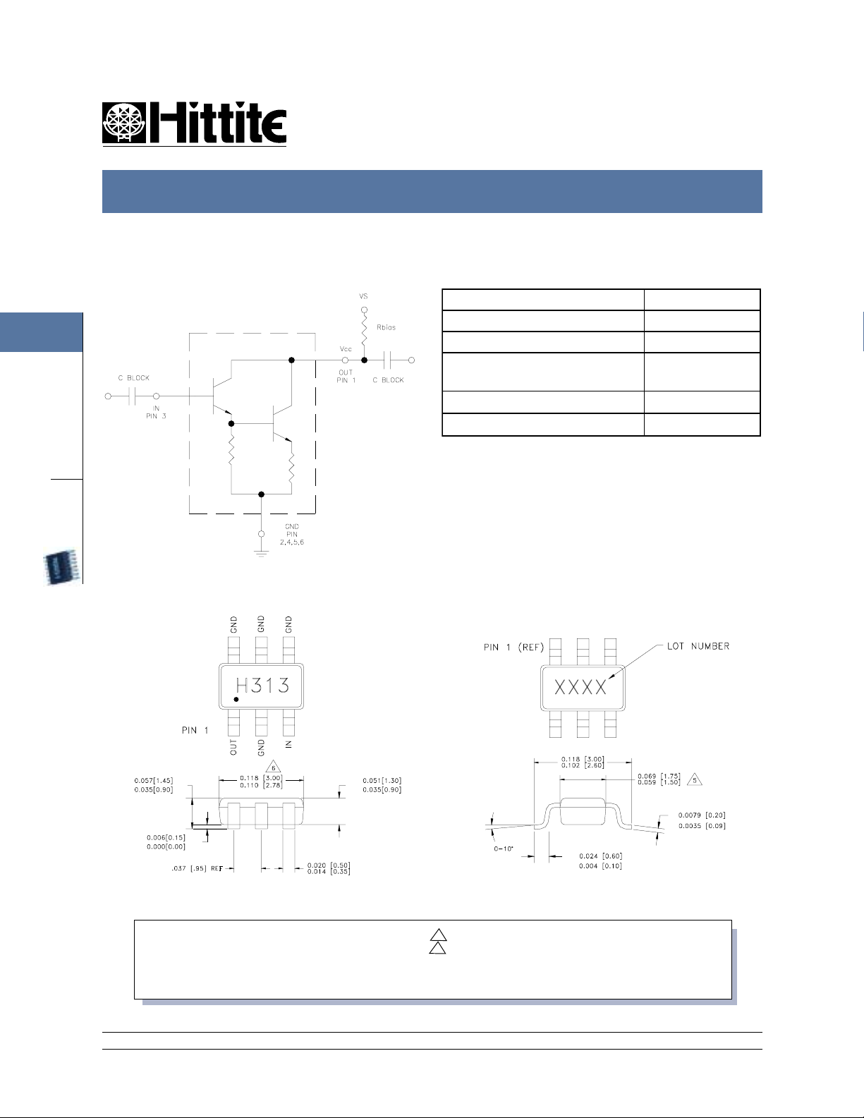
Schematic
1
AMPLIFIERS
SMT
Outline
V00.1100
Absolute Maximum Ratings
)ccV(egatloVylppuScdV5.7+
rewoPtupnImBd02
)cT(erutarepmeTlennahCC°571
o
)C
56=aT(ssidPsuounitnoC
)C°56evobaC/Wm99.3etared(
erutarepmeTegarotSC°051+ot56-
erutarepmeTgnitarepOC°56+ot55-
Note:
1. Select Rbias to achieve desired Vcc voltage
on Pin 1.
2. External blocking capacitors are required on
Pins 1 and 3.
3. See page 8 - 40 for HMC313 Application Circuit.
Wm934
1. MATERIAL:
A) PACKAGE BODY - LOW STRESS INJECTION-MOLDED PLASTIC.
B) LEADFRAME & PADDLE MATERIAL: COPPER ALLOY
2 . PLATING : LEAD & PADDLE- TIN SOLDER PLATE
3. DIMENSIONS ARE IN INCHES (MILLIMETERS).
UNLESS OTHERWISE SPECIFIED ALL TOL. ARE ±0.005(±0.13).
12 Elizabeth Drive, Chelmsford, MA 01824 Phone: 978-250-3343 Fax: 978-250-3373 Web Site: www.hittite.com
4. DIMENSION DOES NOT INCLUDE MOLDFLASH OF 0.15 MM PER SIDE
5. DIMENSION DOES NOT INCLUDE MOLDFLASH OF 0.25 MM PER SIDE
1 - 124
Page 6
MICROWAVE CORPORATION
HBT BROADBAND AMPLIFIER GAIN BLOCK DC - 6.0 GHz
HMC313
V00.1100
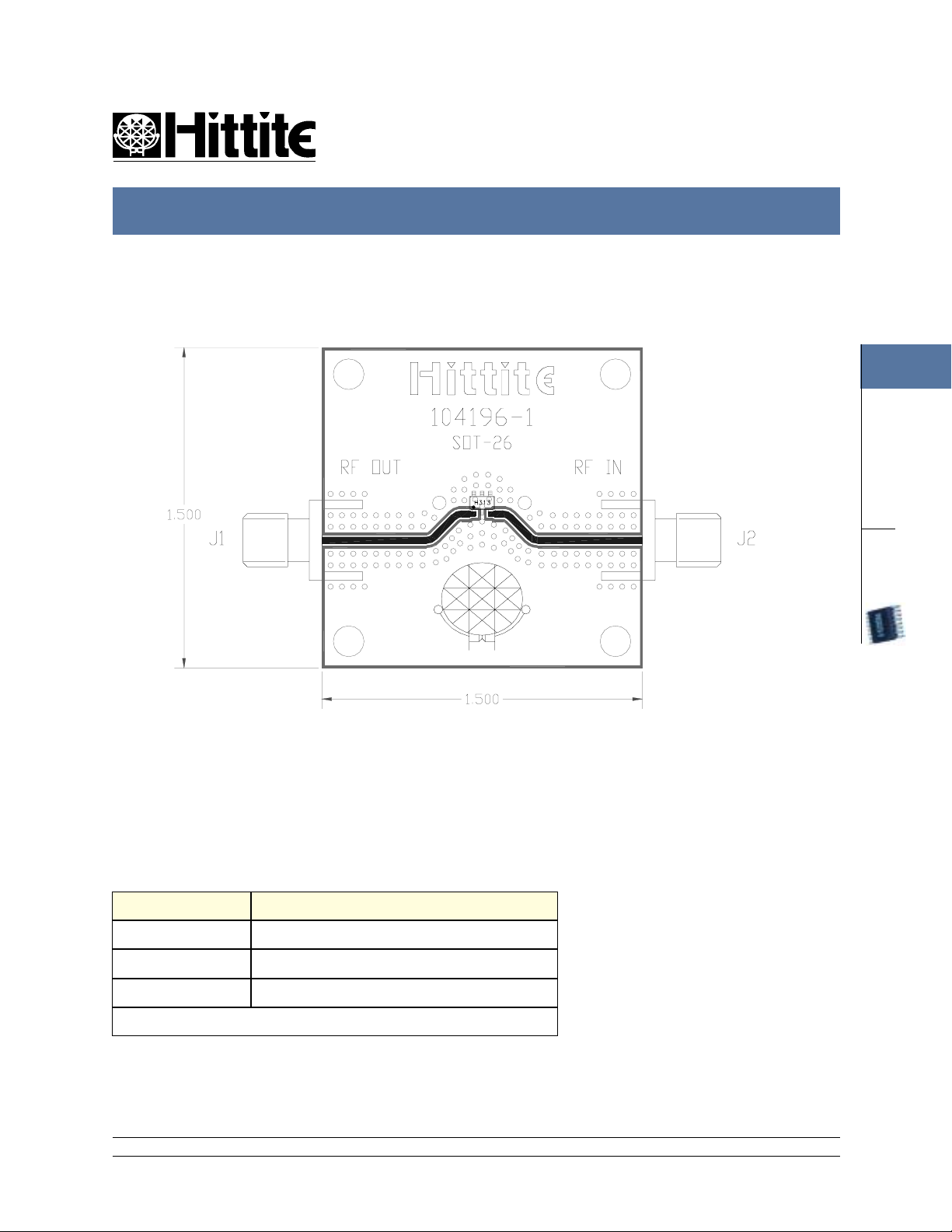
Evaluation PCB Layout for HMC313
FEBRUARY 2001
1
AMPLIFIERS
SMT
The circuit board used in the final application should use RF circuit design techniques. Signal lines should have
50 ohm impedance while the package ground leads should be connected directly to the ground plane similar to
that shown above. A sufficient number of VIA holes should be used to connect the top and bottom ground planes.
The evaluation circuit board as shown is available from Hittite upon request.
Evaluation Circuit Board Layout Design Details
metI noitpircseD
2J-1J rotcennoCAMStnuoMCP
1U 313CMH
*BCP "5.1x"5.1BCPnoitaulavE691401
0534sregoR:lairetaMdraoBtiucriC*
See page 8-40 for "HMC313 Biasing and Impedance Matching Techniques" application note.
12 Elizabeth Drive, Chelmsford, MA 01824 Phone: 978-250-3343 Fax: 978-250-3373 Web Site: www.hittite.com
1 - 125
 Loading...