

Page 1
MICROWAVE CORPORATION
v00.0301
HMC342
GaAs MMIC LOW NOISE
Typical Applications
1
Microwave Point-to-Point Radios
Millimeterwave Point-to-Point Radios
VSAT and other SATCOM Applications
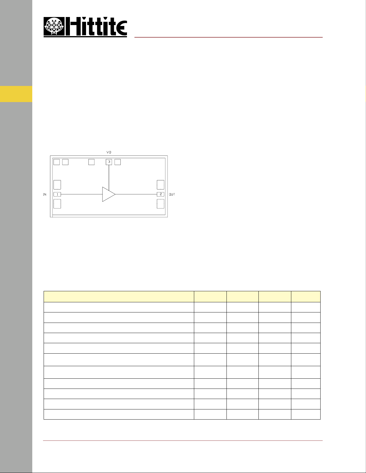
Functional Diagram
AMPLIFIERS - CHIP
AMPLIFIER 13 - 25 GHz
Features
Noise Figure : 3.5 dB
Gain: 20 dB
Single Supply : +3V @ 36 mA
Small Size: 1.06 mm x 2.02 mm
General Description
The HMC342 chip is a GaAs MMIC Low Noise
Amplifi er (LNA) which covers the frequency range
of 13 to 25 GHz. The chip can easily be integrated into Multi-Chip Modules (MCMs) due to its
small (2.14 mm2) size. The chip utilizes a GaAs
PHEMT process offering 20 dB gain from a single
bias supply of + 3.0V @ 36 mA with a noise fi gure
of 3.5 dB. All data is with the chip in a 50 ohm
test fi xture connected via 0.025 mm (1 mil) diameter wire bonds of minimal length 0.31 mm (<12
mils).
1 - 14
Guaranteed Performance, Vdd = +3V, +25° C
retemaraP.niM.pyT.xaMstinU
egnaRycneuqerF 52-31zHG
niaG 510252Bd
erutarepmeTrevOnoitairaVniaG 30.40.C°/Bd
erugiFesioN 5.35.4Bd
ssoLnruteRtupnI 831Bd
ssoLnruteRtuptuO 941Bd
noitalosIesreveR 9354Bd
)Bd1P(noisserpmoCBd1rofrewoPtuptuO 15 mBd
)tasP(rewoPtuptuOdetarutaS 38 mBd
)3PI(tpecretnIredrOdrihTtuptuO 831mBd
)V3+=ddV()ddI(tnerruCylppuS 63Am
For price, delivery, and to place orders, please contact Hittite Microwave Corporation:
12 Elizabeth Drive, Chelmsford, MA 01824 Phone: 978-250-3343 Fax: 978-250-3373
Visit us at www.hittite.com, or Email at [email protected]
Page 2
MICROWAVE CORPORATION
v00.0301
HMC342
GaAs MMIC LOW NOISE
AMPLIFIER 13 - 25 GHz
GaAs MMIC SUB-HARMONICALLY PUMPED MIXER 17 - 25 GHz
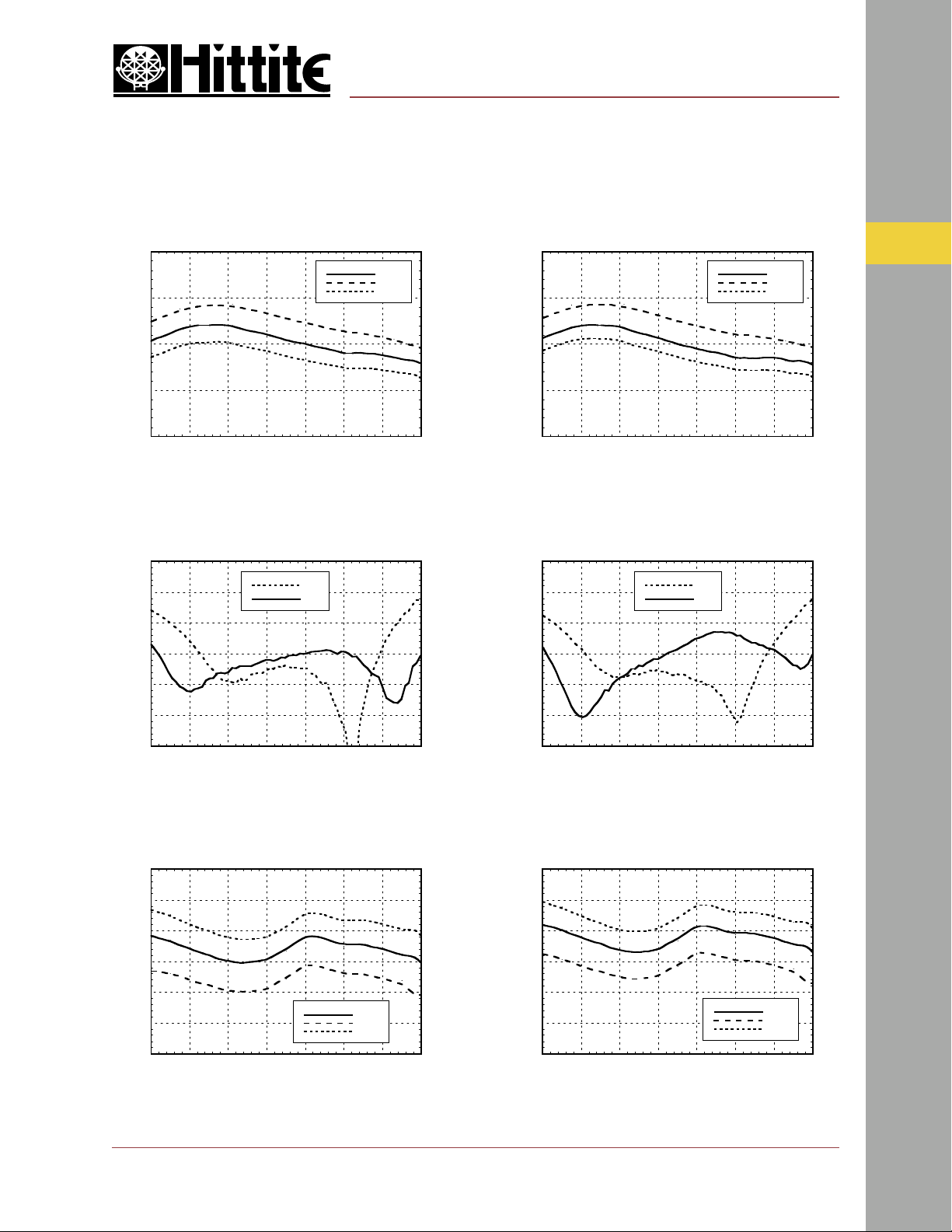
Gain vs. Temperature @ Vdd = +3V Gain vs. Temperature @ Vdd = +5V
30
+25 C
-55 C
25
20
GAIN (dB)
15
10
12 14 16 18 20 22 24 26
FREQUENCY (GHz)
+85 C
Return Loss @ Vdd = +3V Return Loss @ Vdd = +5V
0
-5
-10
S11
S22
30
25
20
GAIN (dB)
15
10
12 14 16 18 20 22 24 26
FREQUENCY (GHz)
0
-5
-10
S11
S22
+25 C
-55 C
+85 C
1
AMPLIFIERS - CHIP
-15
-20
RETURN LOSS (dB)
-25
-30
12 14 16 18 20 22 24 26
FREQUENCY (GHz)
Noise Figure
vs. Temperature @ Vdd = +3V
6
5
4
3
2
NOISE FIGURE (dB)
1
0
12 14 16 18 20 22 24 26
FREQUENCY (GHz)
+25 C
-55 C
+85 C
-15
-20
RETURN LOSS (dB)
-25
-30
12 14 16 18 20 22 24 26
FREQUENCY (GHz)
Noise Figure
vs. Temperature @ Vdd = +5V
6
5
4
3
2
NOISE FIGURE (dB)
1
0
12 14 16 18 20 22 24 26
FREQUENCY (GHz)
+25 C
-55 C
+85 C
For price, delivery, and to place orders, please contact Hittite Microwave Corporation:
12 Elizabeth Drive, Chelmsford, MA 01824 Phone: 978-250-3343 Fax: 978-250-3373
Visit us at www.hittite.com, or Email at [email protected]
1 - 15
Page 3
MICROWAVE CORPORATION
v00.0301
HMC342
GaAs MMIC LOW NOISE
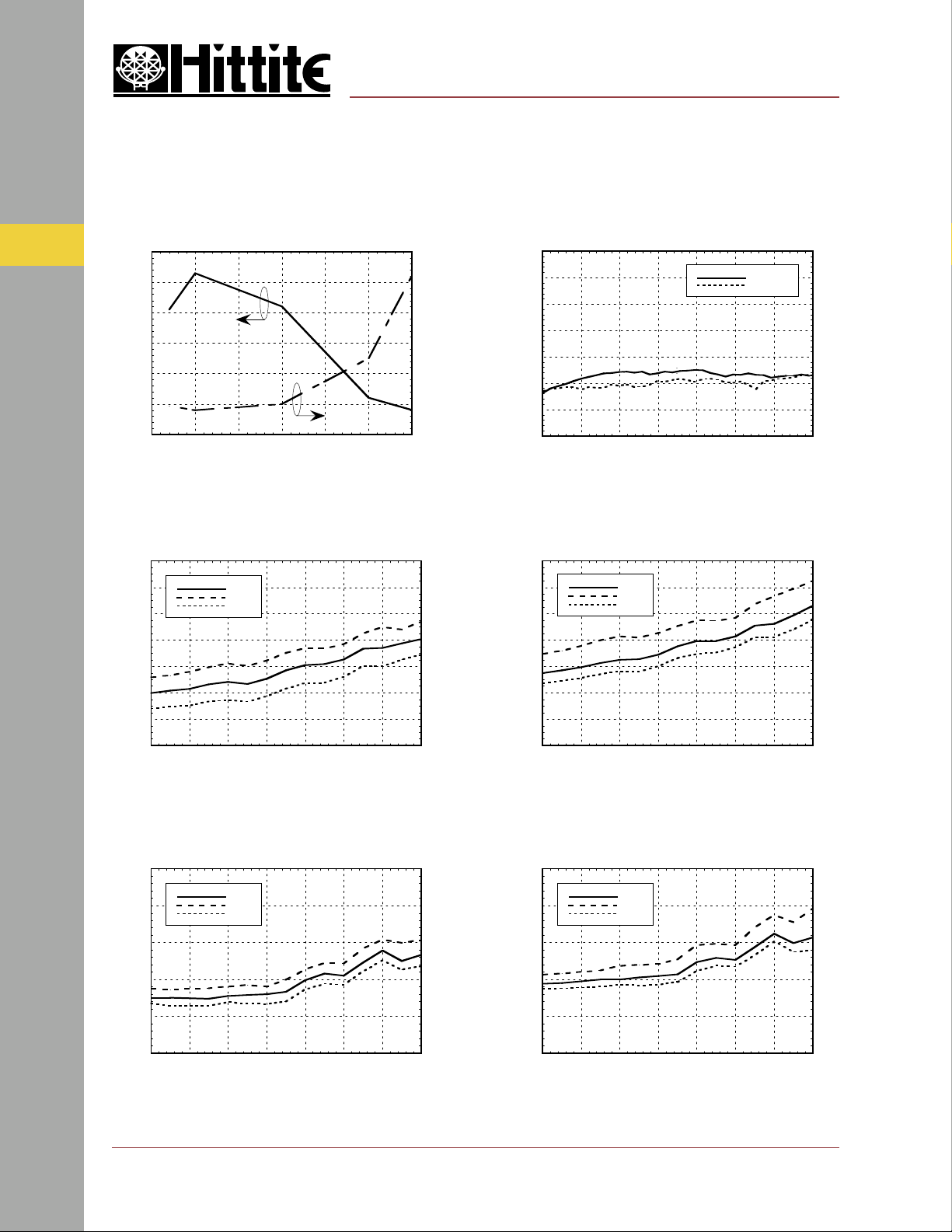
Gain & Noise Figure
vs. Supply Voltage @ 18 GHz
1
21.4
21.3
21.2
21.1
GAIN dB)
21
20.9
20.8
2.5 3 3.5 4 4.5 5 5.5
Vdd SUPPLY VOLTAGE (Vdc)
Output P1dB @ Vdd = +3V Output P1dB @ Vdd = +5V
14
AMPLIFIERS - CHIP
12
10
8
6
P1dB (dBm)
4
2
+25 C
-55 C
+85 C
4
3.8
NOISE FIGURE (dB)
3.6
3.4
3.2
3
2.8
AMPLIFIER 13 - 25 GHz
Isolation
0
-10
-20
-30
-40
ISOLATION (dB)
-50
-60
-70
12 14 16 18 20 22 24 26
FREQUENCY (GHz)
14
12
10
8
6
P1dB (dBm)
4
2
+25 C
-55 C
+85 C
Vdd = +3V
Vdd = +5V
1 - 16
0
12 14 16 18 20 22 24 26
FREQUENCY (GHz)
0
12 14 16 18 20 22 24 26
FREQUENCY (GHz)
Output IP3 @ Vdd = +3V Output IP3 @ Vdd = +5V
30
+25 C
25
20
15
IP3 (dBm)
10
5
12 14 16 18 20 22 24 26
-55 C
+85 C
FREQUENCY (GHz)
For price, delivery, and to place orders, please contact Hittite Microwave Corporation:
12 Elizabeth Drive, Chelmsford, MA 01824 Phone: 978-250-3343 Fax: 978-250-3373
Visit us at www.hittite.com, or Email at [email protected]
30
+25 C
25
20
15
IP3 (dBm)
10
5
12 14 16 18 20 22 24 26
-55 C
+85 C
FREQUENCY (GHz)
Page 4
MICROWAVE CORPORATION
v00.0301
HMC342
GaAs MMIC LOW NOISE
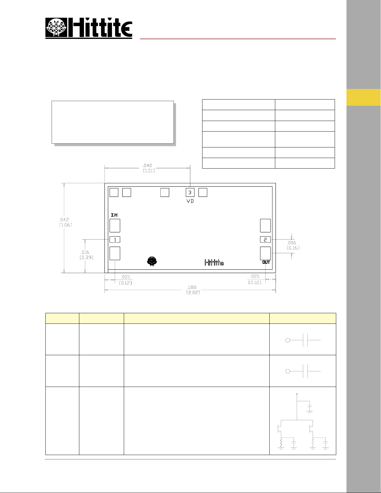
Pad Locations & Outline Drawing
ALL DIMENSIONS IN INCHES (MILLIMETERS)
ALL TOLERANCES ARE ±0.001 (0.025)
DIE THICKNESS IS 0.004 (0.100) BACKSIDE IS GROUND
BOND PADS ARE 0.004 (0.100) SQUARE
BOND PAD SPACING, CTR-CTR: 0.006 (0.150)
BACKSIDE METALLIZATION: GOLD
BOND PAD METALLIZATION: GOLD
AMPLIFIER 13 - 25 GHz
Absolute Maximum Ratings
)ddV(egatloVylppuScdV5.5+
)V3+=ddV()niFR(rewoPtupnImBd0
)cT(erutarepmeTlennahCC°571
)C°58=T(ssidPsuounitnoC
)C°58evobaC°/Wm26.3etared(
erutarepmeTegarotSC°051+ot56-
erutarepmeTgnitarepOC°58+ot55-
Wm623
1
AMPLIFIERS - CHIP
Pad Description
rebmuNdaPnoitcnuFnoitpircseDcitamehcSecafretnI
1tupnIFR zHG52-31morfmho05otdehctamdnadelpuocCAsidapsihT
2tuptuOFR zHG52-31morfmho05otdehctamdnadelpuocCAsidapsihT
3ddV
For price, delivery, and to place orders, please contact Hittite Microwave Corporation:
12 Elizabeth Drive, Chelmsford, MA 01824 Phone: 978-250-3343 Fax: 978-250-3373
.dnuorggnisuohehtotdetcennoc
ebdluohsroticapacehtfoedisdnuorgehT.elbissopsatrohssa
Visit us at www.hittite.com, or Email at [email protected]
roticapacssapybFRlanretxenA.reifilpmaegats-2ehtrofylppusrewoP
ebdluohsroticapacehtothtgneldnobehT.deriuqersiFp003-001fo
1 - 17
Page 5
MICROWAVE CORPORATION
v00.0301
HMC342
GaAs MMIC LOW NOISE
Assembly Diagrams
1
Mounting & Bonding Techniques for Millimeterwave GaAs MMICs
AMPLIFIERS - CHIP
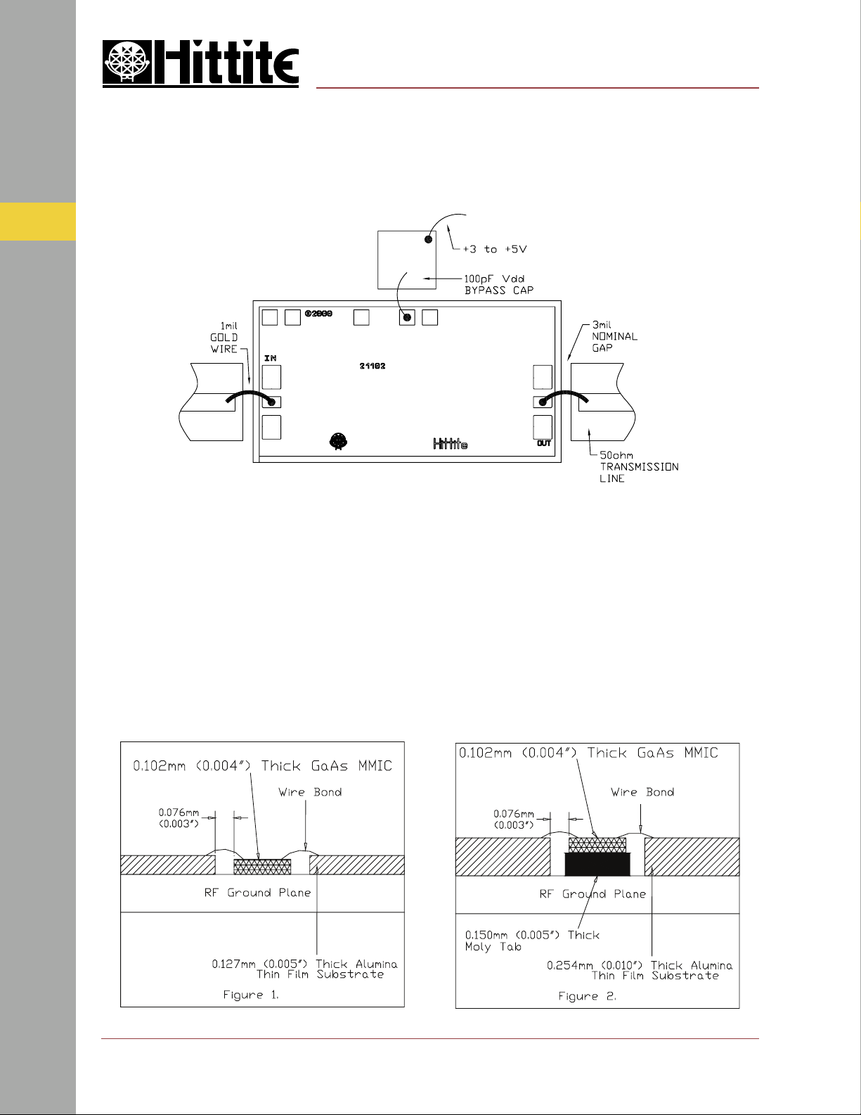
The die should be attached directly to the ground plane eutectically or with conductive epoxy (see HMC general Handling, Mounting, Bonding Note).
AMPLIFIER 13 - 25 GHz
50 Ohm Microstrip transmission lines on 0.127mm (5 mil) thick alumina thin fi lm substrates are recommended for bring-
ing RF to and from the chip (Figure 1). If 0.254mm (10 mil) thick alumina thin fi lm substrates must be used, the die
should be raised 0.150mm (6 mils) so that the surface of the die is coplanar with the surface of the substrate. One
way to accomplish this is to attach the 0.102mm (4 mil) thick die to a 0.150mm (6 mil) thick molybdenum heat spreader
(moly-tab) which is then attached to the ground plane (Figure 2).
Microstrip substrates should brought as close to the die as possible in order to minimize bond wire length. Typical dieto-substrate spacing is 0.076mm to 0.152 mm (3 to 6 mils).
An RF bypass capacitor should be used on the Vdd input. A 100 pF single layer capacitor (mounted eutectically or by
conductive epoxy) placed no further than 0.762mm (30 Mils) from the chip is recommended.
1 - 18
For price, delivery, and to place orders, please contact Hittite Microwave Corporation:
12 Elizabeth Drive, Chelmsford, MA 01824 Phone: 978-250-3343 Fax: 978-250-3373
Visit us at www.hittite.com, or Email at [email protected]
Page 6

MICROWAVE CORPORATION
v00.0301
HMC342
GaAs MMIC LOW NOISE
AMPLIFIER 13 - 25 GHz
GaAs MMIC SUB-HARMONICALLY PUMPED MIXER 17 - 25 GHz
Handling Precautions
Follow these precautions to avoid permanent damage.
Cleanliness:
Handle the chips in a clean environment.
DO NOT attempt to clean the chip using liquid cleaning systems.
Static Sensitivity:
Follow ESD precautions to protect against > ± 250V ESD strikes.
Transients:
Suppress instrument and bias supply transients while bias is applied.
Use shielded signal and bias cables to minimize inductive pick-up.
General Handling:
Handle the chip along the edges with a vacuum collet or with a sharp pair of bent tweezers.
The surface of the chip has fragile air bridges and should not be touched with vacuum collet, tweezers, or fi ngers.
Mounting
1
AMPLIFIERS - CHIP
The chip is back-metallized and can be die mounted with AuSn eutectic preforms or with electrically conductive epoxy.
The mounting surface should be clean and fl at.
Eutectic Die Attach:
A 80/20 gold tin preform is recommended with a work surface temperature of 255 deg. C and a tool temperature of 265
deg. C. When hot 90/10 nitrogen/hydrogen gas is applied, tool tip temperature should be 290 deg. C.
DO NOT expose the chip to a temperature greater than 320 deg. C for more than 20 seconds. No more than 3 seconds
of scrubbing should be required for attachment.
Epoxy Die Attach:
Apply a minimum amount of epoxy to the mounting surface so that a thin epoxy fi llet is observed around the perimeter
of the chip once it is placed into position.
Cure epoxy per the manufacturer’s schedule.
Wire Bonding
Ball or wedge bond with 0.025 mm (1 mil) diameter pure gold wire. Thermosonic wirebonding with a nominal stage
temperature of 150 deg. C and a ball bonding force of 40 to 50 grams or wedge bonding force of 18 to 22 grams is
recommended. Use the minimum level of ultrasonic energy to achieve reliable wirebonds.
Wirebonds should be started on the chip and terminated on the package or substrate. All bonds should be as short as
possible <0.31 mm (12 mils).
For price, delivery, and to place orders, please contact Hittite Microwave Corporation:
12 Elizabeth Drive, Chelmsford, MA 01824 Phone: 978-250-3343 Fax: 978-250-3373
Visit us at www.hittite.com, or Email at [email protected]
1 - 19
 Loading...