

Page 1
查询HMC362供应商
3
MICROWAVE CORPORATION
v02.1202
Typical Applications
Prescaler for DC to X Band PLL Applications:
• Satellite Communication Systems
• Fiber Optic
• Pt-Pt and Pt-MPt Radios
• VSAT
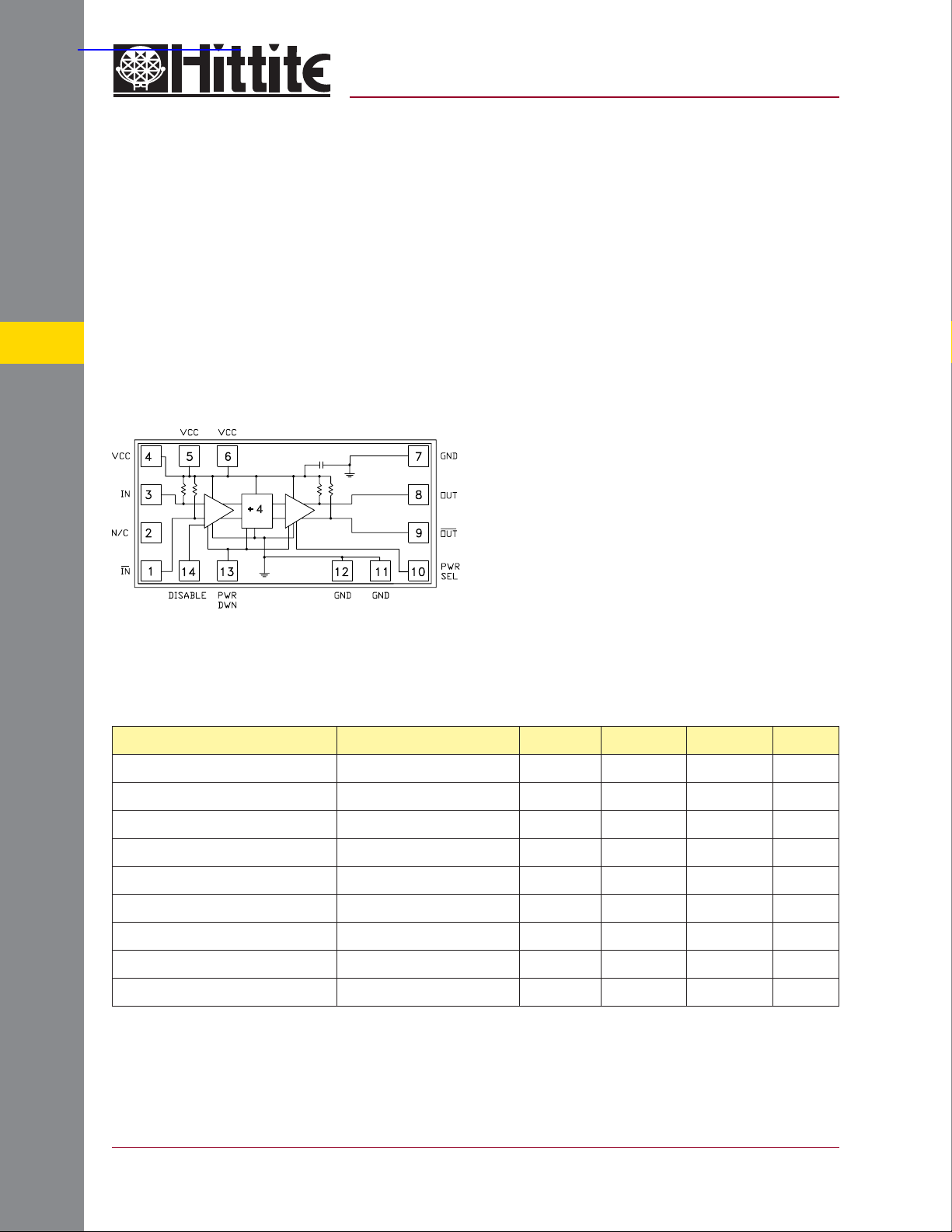
Functional Diagram
HMC362
GaAs HBT MMIC
DIVIDE-BY-4, DC - 11.0 GHz
Features
Ultra Low SSB Phase Noise: -149 dBc/Hz
Wide Bandwidth
Output Power: -6 dBm
Single DC Supply: +5V
Small Size: 0.686 mm x 1.295 mm
General Description
The HMC362 is a low noise Divide-by-4 Static
Divider with InGaP GaAs HBT technology that
has a small size of 0.686 mm x 1.295 mm. This
device operates from DC (with a square wave
input) to 11 GHz input frequency with a single
+5.0V DC supply. The low additive SSB phase
noise of -149 dBc/Hz at 100 kHz offset helps the
user maintain good system noise performance.
Electrical Specifi cations, T
FREQ. DIVIDERS - CHIP
Parameter Conditions Min. Typ. Max. Units
Maximum Input Frequency 11 12 GHz
Minimum Input Frequency Sine Wave Input. [1] 0.2 0.5 GHz
Input Power Range Fin = 1 to 8 GHz -15 >-20 +10 dBm
Output Power [2] Fin = 11 GHz -9 -6 dBm
Reverse Leakage Both RF Outputs Terminated 40 dB
SSB Phase Noise (100 kHz offset) Pin = 0 dBm, Fin = 6 GHz -149 dBc/Hz
Output Transition Time Pin = 0 dBm, Fout = 882 MHz 100 ps
Supply Current (Icc) [2] 68 mA
1. Divider will operate down to DC for square-wave input signal.
2. When operated in low power mode (pin 10 fl oating).
= +25° C, 50 Ohm System,Vcc= 5V
A
Fin = 8 to 11 GHz -10 >-15 +2 dBm
3 - 8
For price, delivery, and to place orders, please contact Hittite Microwave Corporation:
12 Elizabeth Drive, Chelmsford, MA 01824 Phone: 978-250-3343 Fax: 978-250-3373
Order Online at www.hittite.com
Page 2
v02.1202
HMC362
MICROWAVE CORPORATION
GaAs HBT MMIC
DIVIDE-BY-4, DC - 11.0 GHz
GaAs MMIC SUB-HARMONICALLY PUMPED MIXER 17 - 25 GHz
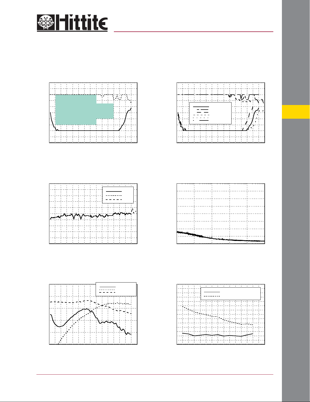
Input Sensitivity Window, T= 25 °C Input Sensitivity Window vs. Temperature
20
10
0
Recommended
Operating Window
-10
INPUT POWER (dBm)
-20
-30
0 1 2 3 4 5 6 7 8 9 10 11 12 13 14 15
INPUT FREQUENCY (GHz)
Output Power vs. Temperature
0
-1
-2
-3
-4
-5
-6
-7
OUTPUT POWER (dBm)
-8
-9
-10
0 1 2 3 4 5 6 7 8 9 10 11 12 13 14 15
INPUT FREQUENCY (GHz)
+25 C
+85 C
-55 C
20
10
0
-10
INPUT POWER (dBm)
-20
-30
0 1 2 3 4 5 6 7 8 9 10 11 12 13 14 15
Min Pin +25 C
Max Pin +25 C
Min Pin +85 C
Max Pin +85 C
Min Pin -55 C
Max Pin -55 C
INPUT FREQUENCY (GHz)
SSB Phase Noise
Performance, Pin= 0 dBm, T= 25 °C
0
-20
-40
-60
-80
-100
-120
SSB PHASE NOISE (dBc/Hz)
-140
-160
2
10
3
10
4
10
OFFSET FREQUENCY (Hz)
5
10
3
FREQ. DIVIDERS - CHIP
6
10
7
10
Output Harmonic
Content, Pin= 0 dBm, T= 25 °C
0
-10
-20
-30
OUTPUT LEVEL (dBm)
-40
-50
0 1 2 3 4 5 6 7 8 9 10 11 12 13 14 15
INPUT FREQUENCY (GHz)
For price, delivery, and to place orders, please contact Hittite Microwave Corporation:
12 Elizabeth Drive, Chelmsford, MA 01824 Phone: 978-250-3343 Fax: 978-250-3373
Reverse Leakage, Pin= 0 dBm, T= 25 °C
Pfeedthru
2nd Harmonic
3rd Harmonic
Order Online at www.hittite.com
0
-10
-20
-30
-40
-50
POWER LEVEL (dBm)
-60
-70
Both Output Ports Terminated
One Output Port Terminated
0 1 2 3 4 5 6 7 8 9 10 11 12 13 14 15
INPUT FREQUENCY (GHz)
3 - 9
Page 3
MICROWAVE CORPORATION
v02.1202
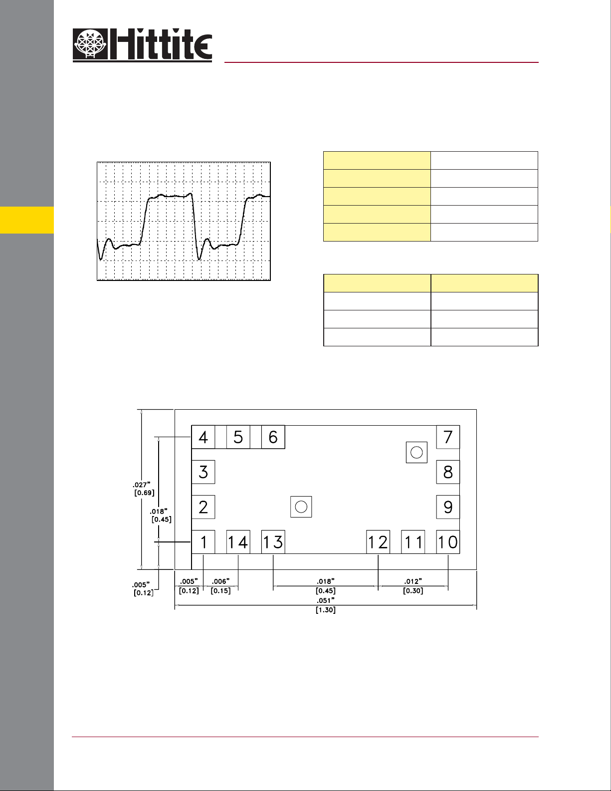
Output V oltage Wavef orm,
Pin= 0 dBm, Fout= 882 MHz, T= 25 °C
HMC362
GaAs HBT MMIC
DIVIDE-BY-4, DC - 11.0 GHz
Absolute Maximum Ratings
3
300
200
100
0
-100
AMPLITUDE (mV)
-200
-300
22.7 22.9 23.1 23.3 23.5 23.7 23.9 24.1 24.3 24.5 24.7
TIME (nS)
Outline Drawing
RF Input (Vcc = +5V) +13 dBm
Vcc +5.5V
VLogic Vcc -1.6V to Vcc -1.2V
Storage Temperature -65 to +150 °C
Operating Temperature -55 to +85 °C
Typical Supply Current vs. Vcc
Vcc (V) Icc (mA)
4.75 61
5.0 68
5.25 74
Note: Divider will operate over full voltage range shown above
FREQ. DIVIDERS - CHIP
For price, delivery, and to place orders, please contact Hittite Microwave Corporation:
3 - 10
12 Elizabeth Drive, Chelmsford, MA 01824 Phone: 978-250-3343 Fax: 978-250-3373
NOTES:
1. ALL DIMENSIONS IN INCHES (MILLIMETERS)
2. ALL TOLERANCES ARE ±0.001 (0.025)
3. DIE THICKNESS IS 0.004 (0.100) BACKSIDE IS GROUND
4. BOND PADS ARE 0.004 (0.100) SQUARE
5. BOND PAD SPACING, CTR-CTR: 0.006 (0.150)
6. BACKSIDE METALLIZATION: GOLD
7. BOND PAD METALLIZATION: GOLD
Order Online at www.hittite.com
Page 4
MICROWAVE CORPORATION
v02.1202
HMC362
GaAs HBT MMIC
DIVIDE-BY-4, DC - 11.0 GHz
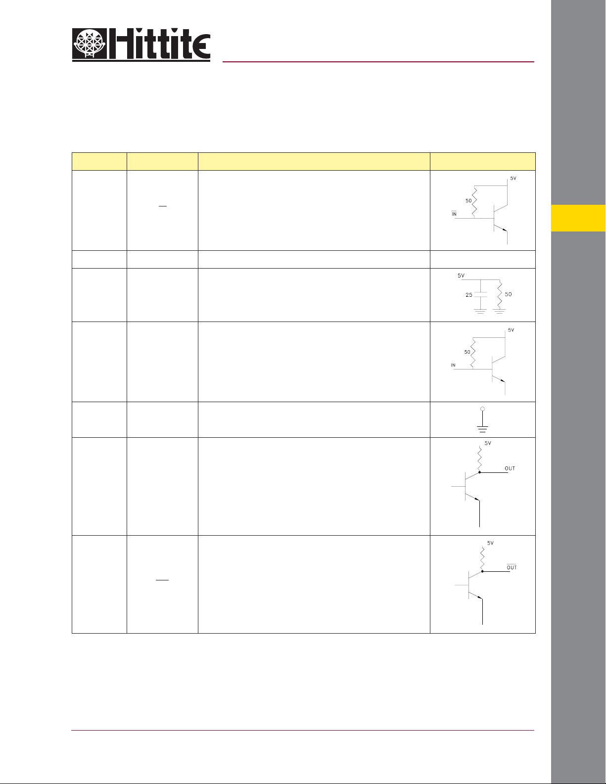
Pad Description
Pad Number Function Description Interface Schematic
1IN
2 N/C Not Connected
4, 5, 6 VCC Supply Voltage 5V ±0.25V can be applied to pad 4, 5, or 6.
3 IN RF Input must be DC blocked.
7, 11, 12 GND Ground: These pads are grounded.
8 OUT Divided Output
RF Input 180° out of phase with pad 3 for differential operation.
AC ground for single ended operation.
3
FREQ. DIVIDERS - CHIP
9 OUT Divided output 180° out of phase with pad 8.
For price, delivery, and to place orders, please contact Hittite Microwave Corporation:
12 Elizabeth Drive, Chelmsford, MA 01824 Phone: 978-250-3343 Fax: 978-250-3373
Order Online at www.hittite.com
3 - 11
Page 5
MICROWAVE CORPORATION
v02.1202
HMC362
GaAs HBT MMIC
DIVIDE-BY-4, DC - 11.0 GHz
Pad Description (continued)
Pad Number Function Description Interface Schematic
3
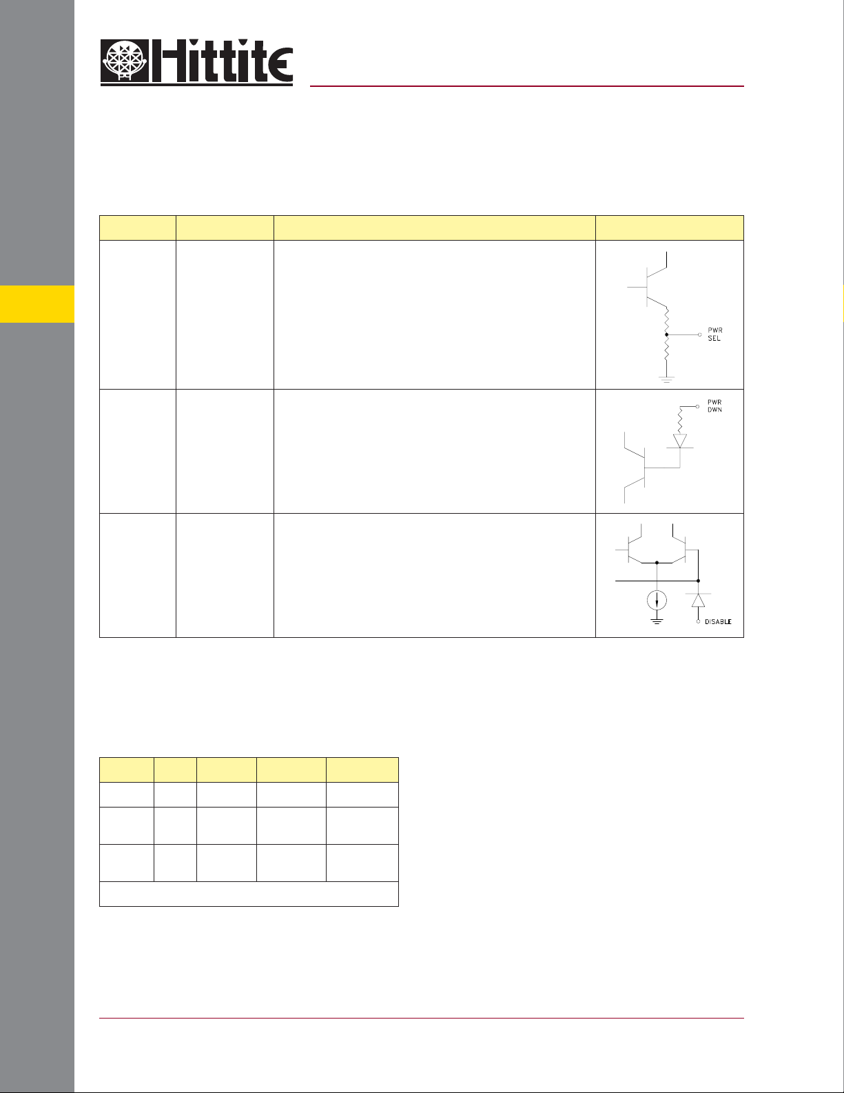
10 PWR SEL
13 PWR DWN
14 DISABLE
FREQ. DIVIDERS - CHIP
In the low power mode, the power select pin is left fl oating.
By grounding this pin, the output power is increased by
approximately 6 dB.
The power down pin is grounded for normal operation.
Applying 5 volts to this pin will power down this device.
The disable pin is grounded for normal operation.
Applying 5 volts to this pin will disable the input buffer amplifi er.
3 - 12
T ruth T able
Function Pin 5V GND Float
DISABLE 14 Output Off Output On X
PWR
DWN
PWR
SEL
X = State not permitted.
13
10 X
For price, delivery, and to place orders, please contact Hittite Microwave Corporation:
12 Elizabeth Drive, Chelmsford, MA 01824 Phone: 978-250-3343 Fax: 978-250-3373
Power
Down
Power
Up
High
Power Output
Power Output
Order Online at www.hittite.com
X
Low
Page 6
MICROWAVE CORPORATION
Assembly Diagram
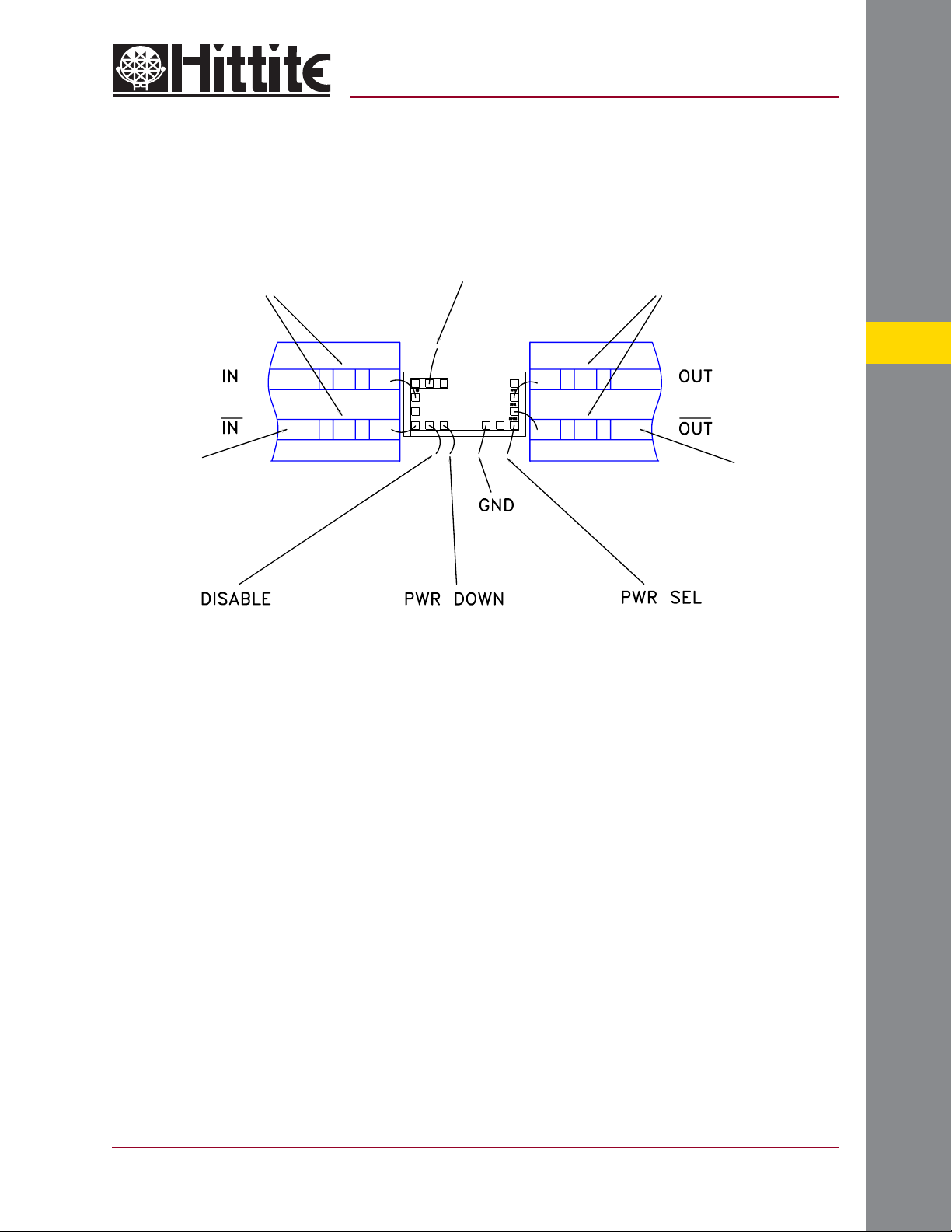
AC coupling capacitors.
v02.1202
To +5V VCC Supply
(Bypassed via 10 uF Capacitor).
HMC362
GaAs HBT MMIC
DIVIDE-BY-4, DC - 11.0 GHz
AC coupling capacitors.
3
Optional AC coupled
differential input. Should
be AC grounded for single
ended operation.
This port should be grounded
for normal operation. Applying
+5V to this port will disable the
input buffer amplifi er.
This port should be grounded
for normal operation. Applying
+5V to this port will power
down the device.
For high power output, this
port should be bonded to
ground. For low power output,
this port should be fl oating.
Optional AC coupled
differential output. For best
single ended reverse leakage
performance, this port should
be terminated into 50 ohm.
Handling Precautions
Follow these precautions to avoid permanent damage.
Cleanliness: Handle the chips in a clean environment. DO NOT attempt to clean the chip using liquid cleaning systems.
Static Sensitivity: Follow ESD precautions to protect against > ± 250V ESD strikes.
Transients: Suppress instrument and bias supply transients while bias is applied. Use shielded signal and bias cables to minimize
inductive pick-up.
General Handling: Handle the chip along the edges with a vacuum collet or with a sharp pair of bent tweezers. The surface of the
chip has fragile air bridges and should not be touched with vacuum collet, tweezers, or fi ngers.
Mounting
The chip is back-metallized and can be die mounted with AuSn eutectic preforms or with electrically conductive epoxy. The mounting
surface should be clean and fl at.
Eutectic Die Attach: A 80/20 gold tin preform is recommended with a work surface temperature of 255 °C and a tool temperature
of 265 °C. When hot 90/10 nitrogen/hydrogen gas is applied, tool tip temperature should be 290 °C. DO NOT expose the chip
to a temperature greater than 320 °C for more than 20 seconds. No more than 3 seconds of scrubbing should be required for
attachment.
Epoxy Die Attach: Apply a minimum amount of epoxy to the mounting surface so that a thin epoxy fi llet is observed around the
perimeter of the chip once it is placed into position. Cure epoxy per the manufacturer’s schedule.
FREQ. DIVIDERS - CHIP
Wire Bonding
Ball or wedge bond with 0.025 mm (1 mil) diameter pure gold wire. Thermosonic wirebonding with a nominal stage temperature of
150 °C and a ball bonding force of 40 to 50 grams or wedge bonding force of 18 to 22 grams is recommended. Use the minimum
level of ultrasonic energy to achieve reliable wirebonds. Wirebonds should be started on the chip and terminated on the package or
substrate. All bonds should be as short as possible <0.31 mm (12 mils).
For price, delivery, and to place orders, please contact Hittite Microwave Corporation:
12 Elizabeth Drive, Chelmsford, MA 01824 Phone: 978-250-3343 Fax: 978-250-3373
Order Online at www.hittite.com
3 - 13
 Loading...