


(without price)
fx-8700GB(LX-388)
JUN. 1992
INDEX
R
CONTENTS
1. |
SCHEMATIC DIAGRAM ................................................................................... |
3 |
2. |
SPECIFICATIONS ............................................................................................. |
4 |
3. |
PIN FUNCTION ................................................................................................. |
5 |
4. |
TROUBLESHOOTING ...................................................................................... |
9 |
5. |
OPERATION CHECK ...................................................................................... |
10 |
6. |
DATA TRANSFER CHECK............................................................................. |
16 |
7. |
EXPLODED VIEW ........................................................................................... |
17 |
8. |
PCB VIEW ....................................................................................................... |
18 |
9. |
PARTS LIST .................................................................................................... |
21 |

1. SCHEMATIC DIAGRAM
— 1 —

— 2 —
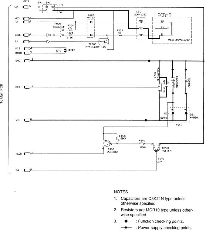
1-3. Power Block
— 3 —

2.SPECIFICATIONS
Program communication functions
RS-232C INTERFACE;
Communication method: Start-stop (Asynchronous)
Transmission speed (baud): 1200 2400 4800 9600BPS
Parity bit: EVEN ODD NONE
Bit length: 8 bit
Stop bit
Transmit: 1 bit
Receive: 2 bit
General
Display system: Liquid crystal display, 10-digit mantissa plus 2-digit exponent. 16 characters by 8 lines (96 by 64 dots).
Power supply: Main — 3 lithium batteries (CR2032)
Memory protection — 1 lithium battery (CR2032)
Power consumption: 0.22W
Battery life: Main — Approximately 100 hours on CR2032
*The battery will also discharge in approximately one year if the unit is left with the power switched off.
Memory protection — Approximately 1 year
*Note that the life of the battery that comes with the unit starts when the battery is loaded in the unit at the factory. The life you get from a battery may be shorter than normal because of the time the unit spends in transport, on the shelf, etc.
*Leaving dead batteries in the unit for a long time can result in demage to the unit. Replace batteries as soon as possible after they get weak or go dead.
Auto power off: Power is automatically switched off approximately 6 minutes after last operation.
Ambient temperature range: 0°C ~ 40°C (32°F ~ 104°F)
Dimensions: 15.6mmH × 81mmW × 172.5mmD (5/8"H × 33/4"W × 63/4"D)
Weight: 179g (6.3oz) including batteries
— 4 —
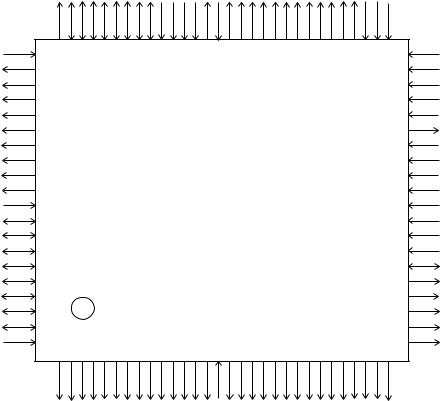
3.PIN FUNCTION
1.CPU (μPD3055GF002-2BA) (IC105)
|
|
H1 |
P7 |
P6 |
P5 |
P4 P3 P2 P1 P0 |
BRK |
INT0 |
INT1 |
INT2 |
KC11 |
GND |
KC10 |
KC9 |
KC8 |
KC7 |
KC6 |
KC5 |
KC4 |
KC3 |
KC2 |
KC1 |
KC0 |
KA0 |
KI0 |
KI1 |
KI2 |
|
||||
WENL |
81 |
80 |
79 |
78 |
77 |
76 |
75 |
74 |
73 |
72 |
71 |
70 |
69 |
68 |
67 |
66 |
65 |
64 |
63 |
62 |
61 |
60 |
59 |
58 |
57 |
56 |
55 |
54 |
53 |
52 |
51 |
50 |
H2 |
82 |
|
|
|
|
|
|
|
|
|
|
|
|
|
|
|
|
|
|
|
|
|
|
|
|
|
|
|
|
|
|
49 |
83 |
|
|
|
|
|
|
|
|
|
|
|
|
|
|
|
|
|
|
|
|
|
|
|
|
|
|
|
|
|
|
48 |
|
L1 |
|
|
|
|
|
|
|
|
|
|
|
|
|
|
|
|
|
|
|
|
|
|
|
|
|
|
|
|
|
|
||
|
|
|
|
|
|
|
|
|
|
|
|
|
|
|
|
|
|
|
|
|
|
|
|
|
|
|
|
|
|
|
|
|
L2 |
84 |
|
|
|
|
|
|
|
|
|
|
|
|
|
|
|
|
|
|
|
|
|
|
|
|
|
|
|
|
|
|
47 |
DT |
85 |
|
|
|
|
|
|
|
|
|
|
|
|
|
|
|
|
|
|
|
|
|
|
|
|
|
|
|
|
|
|
46 |
PRO |
86 |
|
|
|
|
|
|
|
|
|
|
|
|
|
|
|
|
|
|
|
|
|
|
|
|
|
|
|
|
|
|
45 |
FR |
87 |
|
|
|
|
|
|
|
|
|
|
|
|
|
|
|
|
|
|
|
|
|
|
|
|
|
|
|
|
|
|
44 |
LP |
88 |
|
|
|
|
|
|
|
|
|
|
|
|
|
|
|
|
|
|
|
|
|
|
|
|
|
|
|
|
|
|
43 |
GC |
89 |
|
|
|
|
|
|
|
|
|
|
|
|
|
|
|
|
|
|
|
|
|
|
|
|
|
|
|
|
|
|
42 |
DE |
90 |
|
|
|
|
|
|
|
|
|
|
|
|
|
|
|
|
|
|
|
|
|
|
|
|
|
|
|
|
|
|
41 |
VDD1 |
91 |
|
|
|
|
|
|
|
|
|
|
|
|
|
|
|
|
|
|
|
|
|
|
|
|
|
|
|
|
|
|
40 |
IO7 |
92 |
|
|
|
|
|
|
|
|
|
|
|
|
|
|
|
|
|
|
|
|
|
|
|
|
|
|
|
|
|
|
39 |
IO6 |
93 |
|
|
|
|
|
|
|
|
|
|
|
|
|
|
|
|
|
|
|
|
|
|
|
|
|
|
|
|
|
|
38 |
IO5 |
94 |
|
|
|
|
|
|
|
|
|
|
|
|
|
|
|
|
|
|
|
|
|
|
|
|
|
|
|
|
|
|
37 |
IO4 |
95 |
|
|
|
|
|
|
|
|
|
|
|
|
|
|
|
|
|
|
|
|
|
|
|
|
|
|
|
|
|
|
36 |
IO3 |
96 |
|
|
|
|
|
|
|
|
|
|
|
|
|
|
|
|
|
|
|
|
|
|
|
|
|
|
|
|
|
|
35 |
IO2 |
97 |
|
|
|
|
|
|
|
|
|
|
|
|
|
|
|
|
|
|
|
|
|
|
|
|
|
|
|
|
|
|
34 |
|
|
|
|
|
|
|
|
|
|
|
|
|
|
|
|
|
|
|
|
|
|
|
|
|
|
|
|
|
|
|
33 |
|
IO1 |
98 |
|
|
|
|
|
|
|
|
|
|
|
|
|
|
|
|
|
|
|
|
|
|
|
|
|
|
|
|
|
|
|
|
|
|
|
|
|
|
|
|
|
|
|
|
|
|
|
|
|
|
|
|
|
|
|
|
|
|
|
|
|
|
32 |
|
IO0 |
99 |
|
|
|
|
|
|
|
|
|
10 |
11 |
12 |
13 |
14 |
15 |
16 |
17 |
18 |
19 |
20 |
21 |
22 |
23 |
24 |
25 |
26 |
27 |
28 |
29 |
30 |
|
VSS |
100 |
1 |
2 |
3 |
4 |
5 |
6 |
7 |
8 |
9 |
31 |
|||||||||||||||||||||
|
|
|
|
|
|
|
|
|
|
|
|
|
|
|
|
|
|
|
|
|
|
|
|
|
|
|
|
|
|
|
|
|
|
|
A0 |
A1 |
A2 |
A3 |
A4 |
A5 |
A6 |
A7 |
A8 |
A9 |
A10 |
A11 |
A12 |
A13 |
VSS |
A14 |
A15 |
RA14 |
RA15 |
RA16 |
RA17 |
RA18 |
RA19 |
WE |
OE |
FE |
CS1 |
CS2 |
CS3 |
EO |
|
KI3
KI4
KI5
KI6
KI7
V2ON
VDD2
VDD1 VOSC OSCI OSCO VSS TEST ONMK SW MDP2 BCON E3
E2
E1
Pin No. |
Signal |
IN/OUT |
Function |
|
|
|
|
1~14, 16, 19, 20 |
A0~A16 |
OUT |
Address bus |
|
|
|
|
15, 39, 100 |
VSS |
IN |
GND (-5V) |
|
|
|
|
24 |
WE |
OUT |
Write enable signal |
|
|
|
|
25 |
OE |
OUT |
Output enable signal |
|
|
|
|
27, 29 |
CS1, CS3 |
OUT |
Chip select signal |
|
|
|
|
30 |
E0 |
OUT |
Chip enable signal |
|
|
|
|
— 5 —
Pin No. |
Signal |
IN/OUT |
Function |
|
|
|
|
|
|
36 |
SW |
IN/OUT |
Switch signal |
|
|
|
|
|
|
37 |
ONMK |
IN |
Voltage detect signal terminal |
|
|
|
|
|
|
38 |
TEST |
IN |
Test terminal |
|
|
|
|
|
|
40, 41 |
OSCO/I |
IN |
Clock terminal |
|
|
|
|
|
|
42 |
VOSC |
IN |
Power supply for clock |
|
|
|
|
|
|
43, 91 |
VDD1 |
IN |
Power supply (0V) |
|
|
|
|
|
|
44 |
VDD2 |
IN |
Power supply |
|
|
|
|
|
|
45 |
V2ON |
OUT |
Power on signal |
|
|
|
|
|
|
46~53 |
KI0~KI7 |
IN |
Key input signal |
|
|
|
|
|
|
54 |
KAC |
OUT |
On key scan signal |
|
|
|
|
|
|
55~63, 65 |
KC0~KC8, KC10 |
OUT |
Key scan signal |
|
|
|
|
|
|
66 |
GND |
IN |
GND (-5V) |
|
|
|
|
|
|
68, 70 |
INT0, INT2 |
IN |
(0V) |
|
|
|
|
|
|
69 |
INT1 |
IN |
Interrupt terminal |
|
|
|
|
|
|
71 |
BRK |
IN |
(0V) |
|
|
|
|
|
|
72~79 |
P0~P7 |
IN/OUT |
IO port terminal |
|
|
|
|
P0 : Data transfer terminal (Output) |
|
|
|
|
P1 : Data transfer terminal (Input) |
|
|
|
|
P6 : Voltage detect signal terminal (Input) |
|
|
|
|
|
|
80, 82 |
H1, H2 |
OUT |
Output port (Low active) |
|
|
|
|
|
|
81 |
WENL |
IN |
GND (-5V) |
|
|
|
|
|
|
83, 84 |
L1, L2 |
OUT |
Output port (High active) |
|
|
|
|
|
|
89 |
GC |
OUT |
Not used |
|
|
|
|
|
|
92~99 |
IO0~IO7 |
IN/OUT |
Data bus |
|
|
|
|
|
|
— 6 —
 Loading...