

Page 1
CTK-611
INDEX
100 RHYTHMS
PITCH BEND MODE VOLUME INTRO SYNCHRO/ENDING
FULL RANGE
CHORD
FINGERED
POWER
CASIO CHORD
NORMAL
MAX
MIN
NORMAL/FILL-IN VAR/FILL-IN
START
STOP
200 TONES
REVERB
REVERB
HALL
STAGE
SYNTH
ROOM
SYNTH
MIXER
MEMORY
MIXER
TEMPO
STEP
MEMORY
MEMORY TRACK/DRUM PAD
CHORD/1 23456
STEP
ACCOMP
VOLUME
GM
FREE
SESSION
LAYER
SPLIT
TOUCH
RESPONSE
DEMO
TRANSPOSE/
TUNE/MIDI
FREE
SESSION
LAYER
SPLIT
TOUCH
RESPONSE
RHYTHM TONE
CURSOR
ENTER
ENVELOPE
AMP
PITCH
ENVELOPE
ENVELOPE
000-048 DECAY 00 FLAT
049-137 SUSTAIN 01-19 VIBRATO
20-49 OTHERS
CTK-611
ELECTRONIC KEYBOARD
Page 2

CONTENTS
Specifications................................................................................................................................... 1
Block Diagram.................................................................................................................................. 3
Circuit Description............................................................................................................................ 4
Adjustment ..................................................................................................................................... 11
Major Waveforms ........................................................................................................................... 12
Printed Circuit Boards .................................................................................................................... 13
Schematic Diagrams ...................................................................................................................... 14
Exploded View ............................................................................................................................... 19
Parts List ........................................................................................................................................ 20
Page 3

SPECIFICATIONS
GENERAL
Keyboard: 61 standard-size keys, 5 octaves (with touch response on/off)
Drum pads: 6
Tones: 200 (128 General MIDI, 32 synthesized, 8 drum, 32 user); with layer and
split
Rhythm instrument tones: 51
Polyphony: 24 notes maximum (12 for certain tones)
Digital effects: 3 reverb types (HALL, STAGE, ROOM)
Auto accompaniment
Rhythm patterns: 100
Tempo: Variable (216 steps, = 40 to 255)
Chords: 3 fingering methods (CASIO CHORD, FINGERED, FULL RANGE
CHORD)
Rhythm controller: START/STOP, INTRO, NORMAL/NORMAL FILL-IN, VARIATION/VARI-
ATION FILL-IN, SYNCHRO/ENDING
Accomp volume: 0 to 127 (128 steps)
Free session
Number of patterns: 100 (auto-accompaniment in accordance with selected chord progres-
sion)
Memory function
Songs: 2
Recording tracks: 6 (2 through 6 are melody tracks)
Recording methods: Real-time, step
Memory capacity: Approximately 5,200 notes (total for two songs)
Edit function: Equipped
Demo tunes: 2
Synthesizer function
Parameters: PCM set, amp envelope set, attack rate, release rate, pitch envelope set,
pitch, level, touch sense, pan
Mixer function
Channels: 16
Parameters: Program change number, volume, expression, pan, coarse tuning, fine
tuning, on/off/solo
MIDI: 16 multi-timbre receive, GM Level 1 standard
Other functions
Pitch bend range: 12 semitones upwards and downwards
Transpose: 25 steps (–12 semitones to +12 semitones)
Tuning: Variable (A4 = approximately 440 Hz ± 50 cents)
Terminals
MIDI terminals: IN, OUT
Assignable terminal: Standard jack (sustain, sostenuto, soft, rhythm start/stop)
Headphone/Output terminal: Stereo standard jack
Output Impedance: 120 Ω
Output Voltage: 4.5 V (RMS) MAX
Power supply terminal: 9 V DC
Power supply: Dual power supply system
Batteries: 6 D-size batteries
Battery life: Approximately 5 hours continuous operation on manganese batteries
AC adaptor: AD-5
Auto power off: Turns power off approximately six minutes after last key operation. En-
abled under battery power only, can be disabled manually.
Speaker output: 2.5 W + 2.5 W
Power consumption: 9 V --- 7.7 W
Dimensions (HWD): 93.1 × 37.3 × 12.0 cm (36 11/16 × 14 11/16 × 4 3/4 inches)
Weight: Approximately 5.0 kg (11.0 lbs) (without batteries)
— 1 —
Page 4
ELECTRICAL
Current drain with 9 V DC:
No sound output 340 mA ± 20 %
Maximum volume 1012 mA ± 20 %
with 12 keys from C3 to B3 pressed in Square wave tone
Volume: maximum, Touch response: maximum
Reverb: Hall
Phone output level (Vrms with 8 Ω load each channel): L-ch 90 mV ± 20 %
with key C6 pressed in Bassoon tone R-ch 100 mV ± 20 %
Volume: maximum, Touch response: maximum
Reverb: Hall
Speaker output level (Vrms with 4 Ω load each channel): L-ch 1150 mV ± 20 %
with key F5 pressed in Bassoon tone R-ch 1000 mV ± 20 %
Volume: maximum, Touch response: maximum
Reverb: Hall
Output level (Vrms with 47k Ω load each channel): L-ch 1200 mV ± 20 %
with key F5 pressed in Bassoon tone R-ch 1000 mV ± 20 %
Volume: maximum, Touch response: maximum
Reverb: Hall
Minimum operating voltage: 6.3 V
About General MIDI
General MIDI standardizes MIDI data for all sound source types, regardless of manufacturer. General MIDI
specifies such factors as tone numbering, drum sounds, and available MIDI channels for all sound sources.
This standard makes it possible for all MIDI equipment to reproduce the same nuances when playing
General MIDI data, regardless of the manufacturer of the sound source.
This keyboard supports General MIDI, so it can be used to play commercially available pre-recorded
General MIDI data and General MIDI data send to it from a personal computer.
— 2 —
Page 5

BLOCK DIAGRAM
Reset IC
IC1
RN5VD40AA
Sound Source ROM
(16M-bit)
LSI3
UPD23C16000WGX-
C51
Effect RAM
(256K-bit)
LSI5
TC55257DFL-
70L(EL)
RESET
MA0 ~ MA19
MA0, MA1
EA0 ~
EA14
EIO0 ~
EIO7
Working Storage
RAM (256K-bit)
LSI4
TC55257DFL-70L(EL)
MA0
~
MA14
MD0 ~ MD15
MD0
~
MD7
DSP
LSI2
HG51B277FB-1
MIDI
LRCK, SO
BCK, SINK
INOUT
UPD913GF-3BA
P10, P13
P14, P17
CPU
LSI1
NMI
PA0 ~ PA5
PB0 ~ PB3
P23
FI10
LCD Driver
LSI401
SED1278F2A
FI0 ~ FI9
SI0 ~ SI9
KC0 ~ KC7
KI0 ~ KI2
PB0 ~ PB3
VDD
SEG1 ~ SEG40
LCD
COM1 ~ COM16
Keyboard
Power Switch
Buttons
Speakers
Output
LRCK
SO
BCK
D/A Converter
LSI6
UPD6379GR
Filter
Q107 ~ Q110
Main
Volume
Power Amplifier
IC101
TA8248K
PB4
APO
Assingnable Jack
VCC
AVDD
Power Supply Circuit
Q101 ~ Q105,
D106/107, D190
DVDDLVDD
VDD
VC
— 3 —
Page 6

CIRCUIT DESCRIPTION
KEY MATRIX
KC0 KC1 KC2 KC3 KC4 KC KC6 KC7
FI0 C2 (1) C#2 (1) D2 (1) D#2 (1) E2 (1) F2 (1) F#2 (1) G2 (1)
SI0 C2(2) C#2 (2) D2 (2) D#2 (2) E2 (2) F2 (2) F#2 (2) G2 (2)
FI1 G#2 (1) A2 (1) A#2 (1) B2 (1) C3 (1) C#3 (1) D3 (1) D#3 (1)
SI1 G#2 (2) A2 (2) A#2 (2) B2 (2) C3 (2) C#3 (2) D3 (2) D#3 (2)
FI2 E3 (1) F3 (1) F#3 (1) G3 (1) G#3 (1) A3 (1) A#3 (1) B3 (1)
SI2 E3 (2) F3 (2) F#3 (2) G3 (2) G#3 (2) A3 (2) A#3 (2) B3 (2)
FI3 C4 (1) C#4 (1) D4 (1) D#4 (1) E4 (1) F4 (1) F#4 (1) G4 (1)
SI3 C4 (2) C#4 (2) D4 (2) D#4 (2) E4 (2) F4 (2) F#4 (2) G4 (2)
FI4 G#4 (1) A4 (1) A#4 (1) B4 (1) C5 (1) C#5 (1) D5 (1) D#5 (1)
SI4 G#4 (2) A4 (2) #4 (2) B4 (2) C5 (2) C#5 (2) D5 (2) D#5 (2)
FI5 E5 (1) F5 (1) F#5 (1) G5 (1) G#5 (1) A5 (1) A#5 (1) B5 (1)
SI5 E5 (2) F5 (2) F#5 (2) G5 (2) G#5 (2) A5 (2) A#5 (2) B5 (2)
FI6 C6 (1) C#6 (1) D6 (1) D#6 (1) E6 (1) F6 (1) F#6 (1) G6 (1)
SI6 C6 (2) C6# (2) D6 (2) D#6 (2) E6 (2) F6 (2) F#6 (2) G6 (2)
FI7 G#6 (1) A6 (1) A#6 (1) B6 (1) C7 (1)
SI7 G#6 (2) A6 (2) A#6 (2) B6 (2) C7 (2)
BUTTON MATRIX
KC0 KC1 KC2 KC3 KC4 KC5 KC6 KC7
Drum Pad Drum Pad Pitch Bend H
FI10
KI0
KI1
KI2
PB0
PB1 Fingered
PB2 Casio Chord
PB3 Normal
31HEnter
Drum Pad Drum Pad Pitch Bend Start/
42GStop
Drum Pad
5 H
Drum Pad
6 G Tune/MIDI
PA0 PA1 PA2 PA3
Full Range
Chord Response
Step
Memory
Normal/
Synchro/
Ending
Variation/
Tempo
Tempo
Intro
Fill-In Volume
Fill-In
E 7 2 0 Demo
F 45 1
Touch
Free Session
Layer Synth
Split Mixer
9 6 + Tone
8 3 — Rhythm
Transpose/
Reverb
Accomp
— 4 —
Page 7
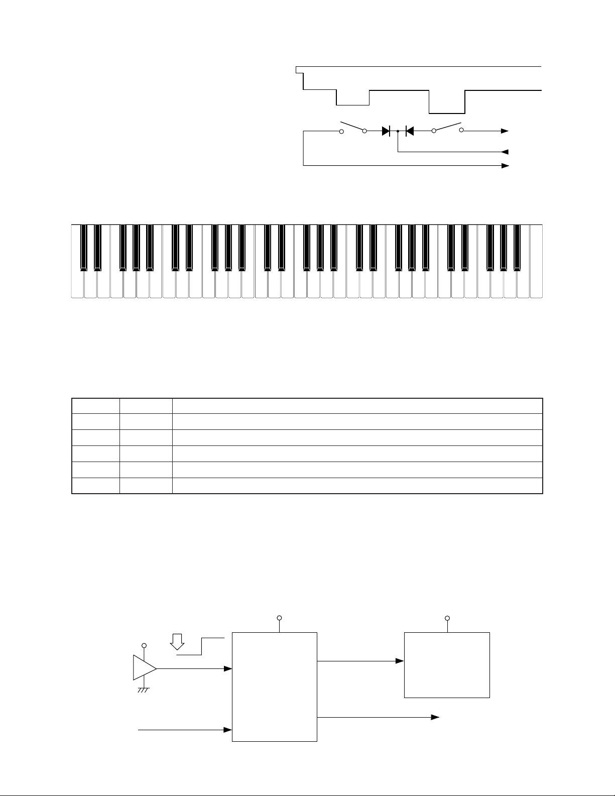
Note: Each key has two contacts,
the first conatct (1) and second contact (2).
NOMENCLATURE OF KEYS
Second contact (2)
Key
First contact (1)
FI
KC
SI
C#2
C2 D2E2F2
F#2D#2
G2
A2 B2 C3 D3
C#3A#2G#2
F#3 G#3
D#3
E3
F3 G3 A3 B3 C4 D4 E4 F4 G4 A4 B4 C5 D5 E5 F5 G5 A5 B5
A#3 C#4 D#4
F#4 G#4
A#4
C#5
D#5
F#5 G#5
A#5
C#6
C6
G#6F#6D#6
A#6
B6A6G6F6E6D6
POWER SUPPLY CIRCUIT
The power supply circuit generates five voltages as shown in the following table. VDD voltage is always
generated. The others are controlled by APO signal from the CPU.
Name Voltage For operation of
VDD +5 V CPU, Reset IC, DSP, Sound source ROM, Working storage RAM, Effect RAM
DVDD +5 V LCD driver, Power jack, Sustain jack, MIDI jack
AVDD +5 V DAC, Filter
LVDD +5.6 V LCD dirver
VCC +9 V Power amplifier, Pilot lamp
C7
RESET CIRCUIT
When batteries are set or an AC adapter is connected, the reset IC provides a low pulse to the CPU. The
CPU then initializes its internal circuit, and clears the working storage RAM.
When the power switch is pressed, the CPU receives a low pulse of POWER signal. The CPU sends APO
signal to the power supply circuit, also sends a reset signal to the DSP.
Battery set
VDD
Reset IC
IC1
RN5VD40AA
POWER
From power switch
RESET
VDD
CPU
LSI1
UPD913GF-3BA
SCKO
NMI
— 5 —
Reset signal
PLE
HG51B277FB-1
APO
To power supply circuit
VDD
DSP
LSI2
Page 8

CPU (LSI1: UPD913GF-3BA)
The 16-bit CPU contains a 1k-byte RAM, three 8-bit I/O ports, two timers, a key controller and serial interfaces.
The CPU detects key velocity by counting the time between first-key input signal FI and second-key SI from
the keyboard. The CPU reads sound data and velocity data from the sound source ROM in accordance with
the selected tone; the CPU can read rhythm data simultaneously when a rhythm pattern is selected. Then the
CPU provides 16-bit serial sound data to the DSP. The CPU also controls MIDI input/output and stores
sequencer data into the working storage RAM.
The following table shows the pin functions of LSI1.
Pin No. Terminal In/Out Function
1 TXD0 Out MIDI signal output
2 RXD0 In MIDI signal input
3 SCK0 Out APO (Auto Power Off) signal output
4, 5 TXD1, RXD2 In/Out Data bus for the LCD driver
6 SCK1 Out 1 MHZ synchronizing pulse output
7 AVCC In DVDD (+5 V) source
AC adaptor detection terminal.
8 AN0 In
9 AN1 — Not used. Connected to ground.
10 AGND In Ground (0 V) source
11 BCK Out Bit clock output
12 SO Out Serial sound data output
13 LRCK Out Word clock output
14 GND In Ground (0 V) source
15, 16 XLT0, XLT1 In/Out 20 MHz clock input/output
17 VCC In +5 V source
18, 19 MD0, MD1 In Mode selection terminal
20 RSTB In Reset signal input
21 NMI In Power ON signal input
22 INT/P10 In/Out Data bus for the LCD driver
23 ~ 30
31 ~ 38 KC0 ~ KC7 Out Terminal for key scan signal
39 ~ 46
47 ~ 50
51 FI10 In Terminal for button input signal
52 SI10/P23 Out Chip enable signal for the LCD driver
53 ~ 55 KI0 ~ KI2 In Terminal for button input signal
56 MWNB Out Write enable signal for the DSP
57 ~ 76 MA0 ~ MA17 Out Address bus
77 MCSB0 Out Chip enable signal output for the sound source ROM
78 MCSB1 Out Not used
79 MCSB2 Out Chip enable signal output for the DSP
FI0 ~ FI3
SI0 ~ SI3
FI4 ~ FI7
SI4 ~ SI7
FI8, FI9
SI8, SI9
In Terminal for key input signal
In Terminal for key input signal
— Not used
+5 V when the keyboard is powered by batteries and becomes
V to cancel the APO function when AC adaptor is connected.
0
— 6 —
Page 9

Pin No. Terminal In/Out Function
80 VCC In +5 V source
81 GND In Ground (0 V) source
82 MRDB Out Read enable signal output for the sound source ROM
83 ~ 98 MD0 ~ MD15 In/Out Data bus
99 PLE Out Reset signal output for the DSP
100 P17 In/Out Data bus for the LCD driver
DIGITAL SIGNAL PROCESSOR (LSI2: HG51B227FB-1)
The DSP receives 16-bit serial sound data output from the CPU and adds the selected effect to the sound data
using the effect RAM. Then the DSP provides the sound data to the DAC. The DSP also controls button input/
output.
The following table shows the pin functions of LSI2.
Pin No. Terminal In/Out Function
1 ~ 3, 80 PB0 ~ PB3 In Button input terminals
4 PB4 In ASSIGNABLE Jack input
5 SO Out Serial sound data output for the DAC
6 WCKO Out Word clock output for the DAC
7 VDD3 In +5 V source
8 TEST — Not used
9 RESB In Reset signal input
10 VSS2 In Ground (0 V) source
11, 12 XIN, XOUT In/Out 20 MHz clock input/output
13 WCKI In Word clock input from the CPU
14 SI In Serial sound data input from the CPU
15 BCKI In Bit clock input from the CPU
16 SINC In 1 MHz synchronizing pulse input
17 VDD2 In +5 V source
18 ~ 25 IO0 ~ IO7 In/Out Data bus
26 RCEB Out Chip enable signal output for the working storage RAM
27 VSS3 In Ground (0 V) source
28 AD1 In Address bus
29 OEB Out Output enable signal for working storage RAM
30 WEB In Write enable signal
31 VDD3 In +5 V source
32 CE2 In Chip enable signal input. High active.
33 AD0 In Address bus
34 CE1B In Chip enable signal input. Low active.
35 ~ 41, 43 EIO0 ~ EIO7 In/Out Data bus for the effect RAM
— 7 —
Page 10

Pin No. Terminal In/Out Function
42 , 44, 46 ~ 48,
51 ~ 59, 61
45 ECEB Out Chip enable signal output for the effect RAM
49 EOEB Out Read enable signal output for the effect RAM
50 VSS3 In Ground (0 V) source
60 EWEB Out Write enable signal output for the effect RAM
62, 66, 70, 74, 78 VSS2 In Ground source
63, 67, 71, 75, 79 VDD2 In +5 V source
64, 65, 68, 69,
72, 73
76, 77 PA6/7 Out Not used
EA0 ~ EA12 Out Address bus for the effect RAM
PA0 ~ PA5 Out Button scan signal output
LCD DRIVER (LSI401: SED1278F2A)
The LCD driver can drive a dot matrix LCD having 40 segment and 16 common lines. The LSI contains 240
graphic symbols in the built-in character generator ROM, and stores 80 characters in the built-in display data
RAM. In accordance with command from the CPU, the LSI is capable of displaying up to 16 characters
simultaneously. The following table shows the pin functions of LSI 401.
Pin No. Terminal In/Out Function
1 ~ 22,
63 ~ 80
23 VSS — GND (0 V) source
24, 25 OSC1, OSC2 In/Out
26 ~ 30 V1 ~ V5 In
31, 32 LP, XCLS — Not used
33 VDD In DVDD (+5 V) source
34, 35 FR, DO — Not used
36 RS In
37 R/W In Read/write terminal. High: read, Low: write
38 E In
39 ~ 42 DB0 ~ DB3 — Not used. Connected to GND (0 V)
43 ~ 46 DB4 ~ DB7 In/Out Data bus
47 ~ 62 COM1 ~ COM16 Out Common signal/output
SEG1 ~ SEG40 Out Segment signal output
Terminals for the built-in clock pulse generator. The external
resistor connected determines the oscillation frequency.
LCD drive voltage input.
Those voltages are used for generating the stepped pulse of
the LCD drive signals.
Data/command determination terminal.
High: data, Low: command
Chip enable signal.
High: enable, the writing is done at fall edge.
Low: disenable
— 8 —
Page 11

DAC (LSI6: UPD6379GR)
The DAC receives 16-bit serial data output from the DSP. The data contains digital sound data of the
melody, chord, bass, and percussion for the right and left channels. The DAC converts the data into
analog waveforms and output them to each channel separately.
Synch signal
L OUT
R OUT
DAC
IC6
UPD6379GR
SI
LRCK
CLK
Data
Word clock
WCKO
Bit clock
SO
DSP
LSI2
HG51B277FB
SINC
SI
Word clock
WCKI
Bit clock
BCKI
Data
SCK1
SO
LRCK
BCK
CPU
LSI1
UPD913GF-3BA
FILTER BLOCK
Since the sound signals from the DAC are stepped waveforms, the filter block is added to smooth the
waveforms.
AVDD
AVDD
To main volume
22 Ω
Q110
2SC1740SQ.R
0.01 µF
AG
2.2K
AG AG AG
150PF
270PF
Q107
10K10K10K
560PF
2SC1740SQ.R
1K
22K
AG
6.3V 1000 µ
AG
+
10 V22 µ
10K
18K
From DAC
— 9 —
Page 12

POWER AMPLIFIER (IC101: TA8248K)
The power amplifier is a two-channel amplifier with standby switch.
The following table shows the pin function of IC101.
Pin No. Terminal In/Out Function
1 NC — Not used
2 B.S.2 — Terminal for a bootstrap capacitor
3 OUT2 Out Channel 2 output
4 VCC In +9 V source
5 OUT1 Out Channel 1 output
6 B.S.1 — Terminal for a bootstrap capacitor
7 Power GND In Ground (0 V) source
8 Stand by In Power control signal input. 0 V: Off, +9 V: On
9 DC — Terminal for a decoupling capacitor
10 NF1 In Negative feedback input
11 IN1 In Channel 1 input
12 IN2 In Channel 2 input
13 NF2 In Negative feedback input
14, 15 Pre GND In Ground (0 V) source
— 10 —
Page 13

ADJUSTMENT
DISPLAY PCB
1) Items to be adjusted:
Item Measuring Instrument
Vop voltage setting Voltmeter
2) Adjustment and Test Point Locations
VR401
3) Equipment connection/Procedure
(TOP VIEW)
TP2
Vop voltage setting
Input
Connection
51.74°
LCD
Input
Point
Eye
Input
Signal
Set Voltmeter
Output
TP2
Adjust
VR410
Watching the LCD at a 51.74° angle to the horizontal, adjust Vop
voltage so that unenergized segments are seen dimly.
Output
Connection
Voltmeter TP2
— 11 —
Output
Point
Adjust for
Adjust for 4.3 to 4.4 V reading on voltmeter under the
temparature 20 to 25 °C.
Make fine adjustment according to the following instruction.
Page 14

MAJOR WAVEFORMS
1
2
CH1: 5 V–CH2: 5 V
1 NMI signal
JE connector pin 16
2 APO signal
JD connector pin 9
5
0.5 s
Power button ON
–
50 µs
CH1
CH2
CH1
3
4
CH1: 5 V–CH2: 5 V
3 Button scan signal PA0
JD connector pin 14
4 Button scan signal PA1
JE connector pin 14
Power ON
20 ms
–
0.5 s
CH1
CH2
CH1
9
0
CH1: 50 mV
˜
9 DAC output (L-ch)
JD connector pin 6
0 Dac output (R-ch)
JD connector pin 7
1 ms
CH2: 50 mV
1 ms
CH1
CH1
A
CH2
CH2
B
˜
CH1: 50 mV˜CH2: 50 mV
˜
A Sound signal (L-ch)
JF connector pin 2
B Sound signal (R-ch)
JF connector pin 1
Tone : Whistle (078)
Key : A4
Touch response : Off
Reverb : Off
Volume : Maximum
6
CH1: 5 V–CH2: 5 V
5 Key scan signal KC0
JB connector pin 1
6 Key scan signal KC1
JB connector pin 2
7
CH2
8
–
CH1: 5 V–CH2: 5 V
–
CH2
7 RS signal PA4
JC connector pin 7
8 R/W signal PA5
JC connector pin 6
— 12 —
Page 15

Sub PCB JCM462-MA2M
PRINTED CIRCUIT BOARDS
Main PCB JCM462-MA1M
7
8
1
3
2
10
9
6
Top View
12
11
4
Top View
5
Bottom View
— 13 —
Page 16

Main PCB JCM462-MA1M
SCHEMATIC DIAGRAMS
8
7
4
1
10
3
9
2
56
— 14 —
Page 17

Sub PCB JCM462-MA2M/Volume PCB JCM462-MA3M
12
— 15 —
11
Page 18

Display PCB JCM462-LCD1M
— 16 —
Page 19

Keyboard PCBs JCM617T-KY1M/KY2M
— 17 —
Page 20

LCD
Common
SEG 1
SEG 2
SEG 3
SEG 4
SEG 5
SEG 6
SEG 7
SEG 8
SEG 9
SEG10
SEG11
SEG12
SEG13
SEG14
SEG15
SEG16
SEG17
SEG18
SEG19
SEG20
SEG21
SEG22
SEG23
SEG24
SEG25
SEG26
SEG27
SEG28
SEG29
SEG30
SEG31
SEG32
SEG33
SEG34
SEG35
SEG36
SEG37
SEG38
SEG39
SEG40
COM 1
COM 2
COM 3
COM 4
COM 5
COM 6
COM 7
COM12
COM13
COM14
COM15
Segment
SEG 1
SEG 2
SEG 3
COM16
SEG17
SEG 8
SEG 4
SEG 5
SEG 6
SEG 9
SEG10
SEG 7
SEG 8
SEG 9
SEG32
COM 9
SEG33
SEG10
SEG11
SEG34
SEG35
SEG36
SEG12
SEG13
SEG14
SEG37
SEG38
SEG39
SEG15
SEG16
SEG17
SEG40
SEG 3
COM12
SEG18
SEG19
SEG20
SEG 2
SEG 1
SEG11
SEG21
SEG22
SEG23
COM 9
SEG12
COM16
SEG24
SEG25
SEG26
SEG29
COM15
COM14
SEG27
SEG28
SEG29
COM13
SEG30
SEG31
SEG30
SEG31
SEG32
SEG32
COM12
COM11
SEG33
SEG34
SEG35
COM10
SEG20
COM 9
SEG36
SEG37
SEG38
SEG19
SEG18
SEG39
SEG40
COM 1
COM13
COM14
COM15
COM 2
COM 3
COM 4
COM16
COM10
COM12
COM 5
COM 6
COM 7
SEG21
COM11
COM12
COM13
COM14
COM15
COM16
SEG17
SEG 8
SEG 9
SEG10
SEG32
COM 9
SEG33
SEG34
SEG35
SEG36
SEG37
SEG38
SEG39
SEG40
SEG 3
COM12
SEG 2
SEG 1
SEG11
COM 9
— 18 —
SEG12
COM16
SEG29
COM15
COM14
COM13
SEG30
SEG31
SEG32
COM12
COM11
COM10
SEG20
COM 9
SEG19
SEG18
COM13
COM14
COM15
COM16
COM10
COM12
SEG21
COM11
Page 21

17
27
28
31
29
16
EXPLODED VIEW
R-1
17
13
15
18
19
14
20
26
25
24
23
22
21
12
3
2
1
6
10
7
9
8
R-2
11
30
5
R-3
4
— 19 —
Page 22

PARTS LIST
CTK-611
Notes: This parts list does not include the cosmetic parts, which
parts are marked with item No. "R-X" in the exploded
view.
Contact our spare parts department if you need these
parts for refurbish.
1. Prices and specifications are subject to change without prior notice.
2. As for spare parts order and supply, refer to the
"GUIDEBOOK for Spare parts Supply", published
seperately.
3. The numbers in item column correspond to the same
numbers in drawing.
Page 23

Item Code No. Parts Name Specification Q R
Main PCB
1 6925 8440 PCB/ASS'Y (MA1M) M240613*1 1 B
LSI1 2012 4879 LSI/CPU UPD913GF-3BA(T) 1 A
LSI2 2012 2079 LSI/DSP HG51B277FB-1 1 A
LSI3 2012 5590 LSI/ROM UPD23C16000WGX-C51 1 A
LSI4/LSI5 2012 5572 LSI/RAM TC55257DFL-70L(EL) 2 A
LSI6 2105 4746 LSI/DAC UPD6379GR-E1 1 A
IC1 2012 1883 IC/MOS RN5VD40AA-TR 1 A
MRC1,2,5,6 2845 6456
MRC3,4 2845 6457
X1 2590 2742
X2 2590 2699
Sub PCB ass'y
2
IC101 2114 5775
IC102
Q101 2250 0742
Q103 2251 0672
Q105 2250 1578
D101/D102
D106 2360 1085
D107 2360 1946
D190 2360 1673 DIODE/ZENER
LED101 2320 3146 LED
J101 3501 7049 JACK/POWER HEC2305-01-330 1 C
J102 3612 0665 JACK/PHONE YKB21-5006 1 C
J103 3612 0789 JACK YKB21-5010 1 C
J104 3501 4816 JACK/DIN YKF51-5051 1 C
VR101 2765 2178 VOLUME EWASC2C95B23 1 C
3 6926 8350 PCB/ASS'Y (LCD1M) M240609*2 1 B
LSI401 2012 6018 LSI/LCD DRIVER SED1278F2A 1
VR401 2775 3286 POTENTIOMETER/CHIP EVM3SSX50B53 1
4 6924 2580 PCB/ASS'Y (KY1M) M140211*5 1
D501 - D564 2301 0101 DIODE 1S2473-T-77-T 64
5 6925 8490 PCB/ASS'Y (KY2M) M140212*9 1
D565 - D622 2301 0101 DIODE 1S2473-T-77-T 58
6 6922 2720 KEY SET/LT WHITE M312118*1 4 A
7 6922 2730 KEY SET/LT WHITE M312118*2 1 A
8 6922 2740 KEY SET/10P BLACK M111726-1 2
9 6922 2750 KEY SET/5P BLACK M111726-2 1 A
10 6922 2761 RUBBER/KEY CONTACT M211704A-1 4 C
11 6922 2771 RUBBER/KEY CONTACT M211705A-1 1 C
12 3122 3546
13 3335 6724
14 6926 6971
15 6926 6991
16 6925 8590
6926 9180 PCB/ASS'Y (MA2,3M) M140554*3 1 B
2252 1248 IC/PHOTOCOUPLER HCPL-261A 1 B
2252 0784
2390 3018 DIODE 1T2
2390 1344
Display PCB
Keyboard PCBs
Keyboard unit
Panel unit
Notes: Q Ð Quantity per unit
R-C NETWORK/CHIP
R-C NETWORK/CHIP
OSCILLATOR/CRYSTAL
OSCILLATOR/CERAMIC
IC/LINEAR (POWER AMP)
TRANSISTOR
TRANSISTOR
TRANSISTOR
TRANSISTOR
DIODE
DIODE/ZENER
DIODE/ZENER
MODULE/EL
LCD
SPACER
SPACER
RUBBER/INTERCONNECTOR
R Ð Rank
Ñ 20 Ñ
EZAST62AAAJ 4 C
EZASS508TAJ 2 C
AT-49-30M 1 C
EFOB2005E0 1 C
TA8248K 1 A
2SA1703S,T-AN-T
2SC1740SQ,R-TP-T 7 C
2SB1548-P,CS 1 1
2SC4483S,T-AN 1 C
1SS133T-77-T 40 C
HZS6B1LTD-T 1 C
MTZJ5.6CT-77-T 1 C
MTZJ5.6AT-77-T
TLR124
YLM-102 1 B
LD-B10088E 1 B
M440644A-1 1 C
M440648A-1 1 C
M440426-2 2 B
1C
2C
1
1
C
C
A
C
B
X
B
X
A
Page 24

Item Code No. Parts Name Specification Q R
17 3831 0833
18 6923 4980
19 6925 8610
20 6926 8280
21
22 6926 8290
23 6926 8300
24
25 6906 9071
26 6925 8680
27 6913 6410
28 6921 5030
29 6926 8320
30 6906 9097 COVER/BATTERY M311164G*16 1
31 6926 8520 FILM M440651-1 2
6925 8630
6926 8310 RUBBER/BUTTON M240546-2 1
Accessory
6906 8752 STAND/MUSIC/BAR TYPE M340629B*2 1
6926 8360 STAND/MUSIC/BOARD TYPE M140530-2 1
SPEAKER
RUBBER/BUTTON
RUBBER/BUTTON
RUBBER/BUTTON
RUBBER/BUTTON
RUBBER/BUTTON
RUBBER/BUTTON
RUBBER/BUTTON
RUBBER/BUTTON
SWITCH/SLIDE
KNOB
PLATE/DISPLAY
S12J49A 2 B
M312122-2 1 B
M240543-1 1 B
M140516-2 1 B
M240544-1 1 B
M240544-3 1 B
M240545-2 1 B
M240547-2 1 B
M240548-1 1 B
CSB-12D 1 B
M311859-1 2 B
M240568-3 1 C
B
B
C
B
B
Notes: Q Ð Quantity per unit
R Ð Rank
Ñ 21 Ñ
Page 25

Page 26

CASIO TECHNO CO.,LTD.
Overseas Service Division
8-11-10, Nishi-Shinjuku
Shinjuku-ku, Tokyo 160-0023, Japan
 Loading...