

Page 1
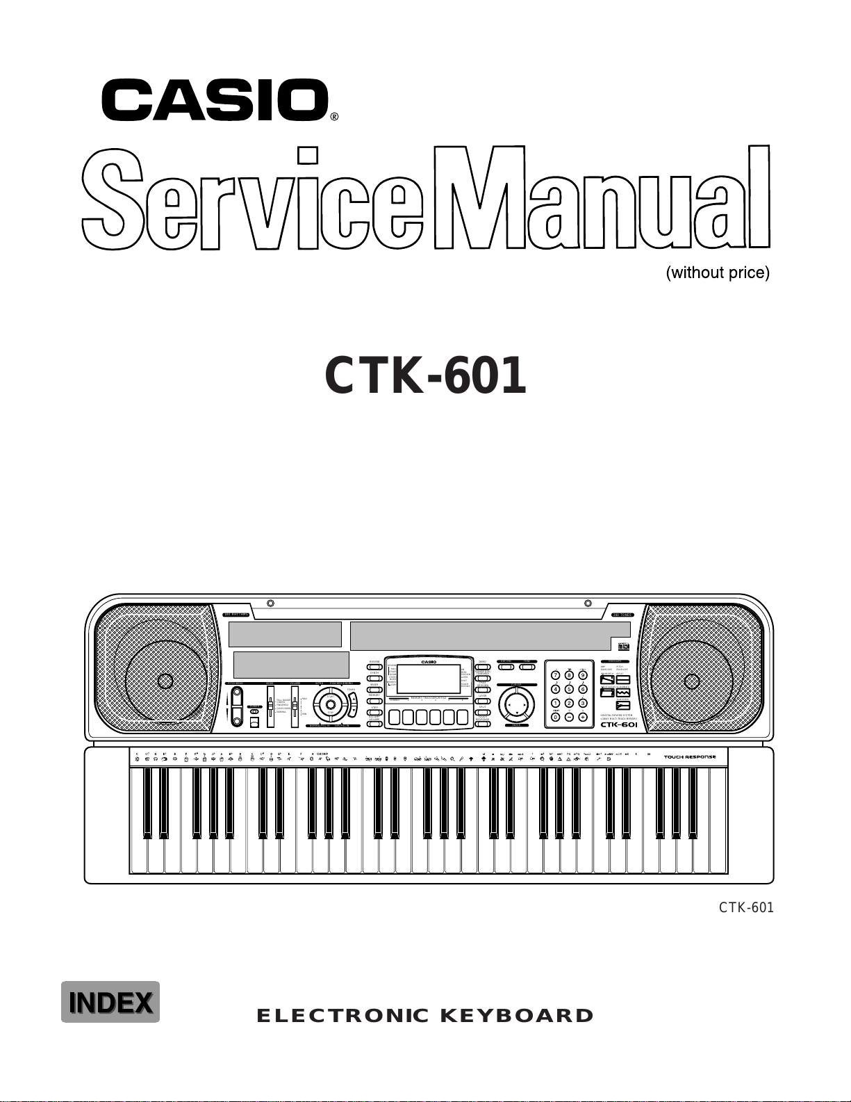
CTK-601
100 RHYTHMS
PITCH BEND MODE VOLUME INTRO SYNCHRO/ENDING
FULL RANGE
CHORD
FINGERED
POWER
CASIO CHORD
NORMAL
MAX
MIN
NORMAL/FILL-IN VAR/FILL-IN
START
STOP
200 TONES
REVERB
REVERB
HALL
STAGE
SYNTH
ROOM
SYNTH
MIXER
MEMORY
MIXER
TEMPO
STEP
MEMORY
MEMORY TRACK/DRUM PAD
CHORD/1 23456
STEP
ACCOMP
VOLUME
GM
FREE
SESSION
LAYER
SPLIT
TOUCH
RESPONSE
TRANSPOSE/
TUNE/MIDI
SESSION
TOUCH
RESPONSE
RHYTHM TONE
DEMO
FREE
CURSOR
LAYER
SPLIT
ENTER
ENVELOPE
AMP
PITCH
ENVELOPE
ENVELOPE
000-048 DECAY 00 FLAT
049-137 SUSTAIN 01-19 VIBRATO
20-49 OTHERS
DIGITAL REVERB SYSTEM
2WAY MULTI-TRACK MEMORY
CTK-601
ELECTRONIC KEYBOARD
Page 2

CONTENTS
Page
Specifications............................................................................................................................................ 1
Block Diagram........................................................................................................................................... 3
Circuit Description..................................................................................................................................... 4
Adjustment .............................................................................................................................................. 11
Major Waveforms .................................................................................................................................... 13
Printed Circuit Boards ............................................................................................................................. 14
Schematic Diagrams ............................................................................................................................... 15
Exploded View ........................................................................................................................................ 20
Parts List ................................................................................................................................................. 21
SPECIFICATIONS
GENERAL
Keyboard: 61 standard-size keys, 5 octaves (with touch response on/off)
Drum pads: 6
Tones: 200 (128 General MIDI, 32 synthesized, 8 drum, 32 user); with layer and
split
Rhythm instrument tones: 51
Polyphony: 24 notes maximum (12 for certain tones)
Digital effects: 3 reverb types (HALL, STAGE, ROOM)
Auto accompaniment
Rhythm patterns: 100
Tempo: Variable (216 steps, = 40 to 255)
Chords: 3 fingering methods (CASIO CHORD, FINGERED, FULL RANGE
CHORD)
Rhythm controller: ST ART/STOP, INTRO, NORMA/FILL-IN, VAR/FILL-IN, SYNCHRO/END-
ING
Accomp volume: 0 to 127 (128 steps)
Free session
Number of patterns 100 (auto-accompaniment in accordance with selected chord progres-
sion)
Memory function
Songs: 2
Recording tracks: 6 (2 through 6 are melody tracks)
Recording methods: Real-time, step
Memory capacity: Approximately 5,200 notes (total for two songs)
Edit function: Equipped
Demo tunes: 2
Synthesizer function
Parameters: PCM set, amp envelope set, attack rate, release rate, pitch envelope set,
pitch, level, touch sense, pan
Mixer function
Channels: 16
Parameters: Program change number, volume, expression, pan, coarse tuning, fine
tuning, on/off/solo
MIDI: 16 multi-timbre receive, GM Level 1 standard
Other functions
Pitch bend range: 12 semitones upwards and downwards
Transpose: 25 steps (–12 semitones to +12 semitones)
Tuning: Variable (A4 = approximately 440 Hz ± 50 cents)
— 1 —
Page 3
Terminals
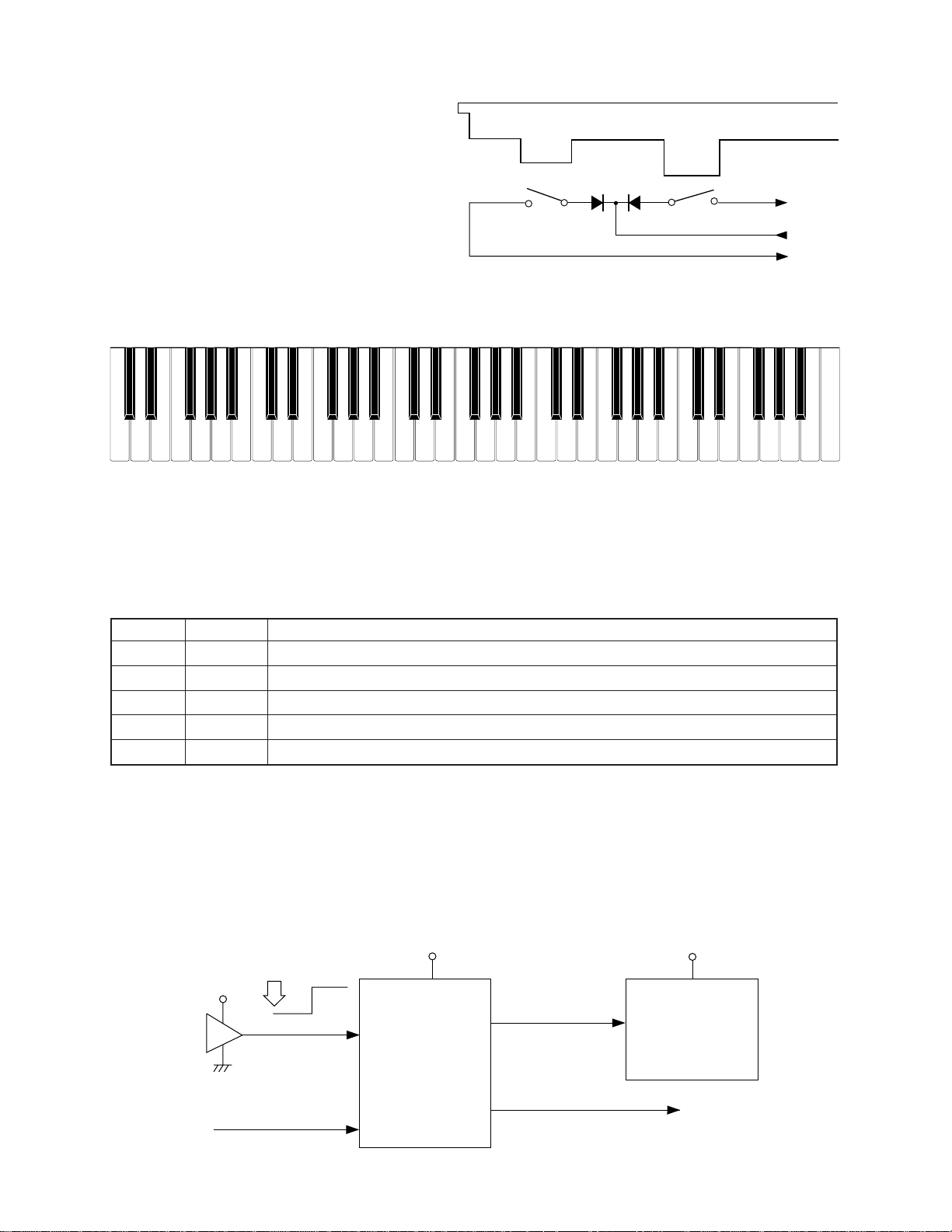
MIDI terminals: IN, OUT
Assignable terminal: Standard jack (sustain, sostenuto, soft, rhythm start/stop)
Headphone/Output terminal: Stereo standard jack
Output Impedance: 120 Ω
Output Voltage: 4.5 V (RMS) MAX
Power supply terminal: 9 V DC
Power supply Dual power supply system
Batteries: Six D-size batteries
Battery life: Approximately 5 hours continuous operation on manganese batteries
AC adaptor: AD-5
Auto power off: Turns power off approximately six minutes after last key operation. En-
abled under battery power only, can be disabled manually.
Power consumption: 9 V --- 7.7 W
Speaker output: 2.5 W + 2.5 W
Dimensions (HWD): 93.1 × 37.3 × 12.0 cm (36 11/16 × 14 11/16 × 4 3/4 inches)
Weight: Approximately 5.0 kg (11.0 lbs) (without batteries)
ELECTRICAL
Current drain with 9 V DC:
No sound output 200 mA ± 20 %
Maximum volume 810 mA ± 20 %
with 12 keys from C3 to B3 pressed in Square wave tone
Volume: maximum, Touch response: maximum
Reverb: Hall
Phone output level (Vrms with 8 Ω load each channel):
with key C6 pressed in Bassoon tone R-ch 100 mV ± 20 %
Speaker output level (Vrms with 4 Ω load each channel):
with key F5 pressed in Bassoon tone R-ch 1000 mV ± 20 %
Minimum operating voltage: 6.3 V
About General MIDI
General MIDI standardizes MIDI data for all sound source types, regardless of manufacturer. General MIDI
specifies such factors as tone numbering, drum sounds, and available MIDI channels for all sound sources.
This standard makes it possible for all MIDI equipment to reproduce the same nuances when playing
General MIDI data, regardless of the manufacturer of the sound source.
This keyboard supports General MIDI, so it can be used to play commercially available pre-recorded
General MIDI data and General MIDI data send to it from a personal computer.
— 2 —
Page 4
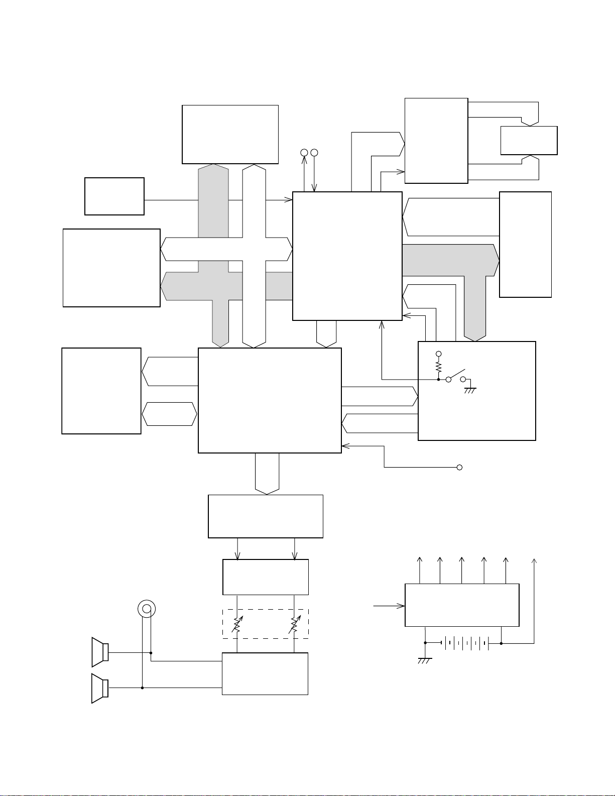
KC0 ~ KC7
FI0 ~ FI9
SI0 ~ SI9
KI0 ~ KI2
PB0 ~ PB3
P10, P13
P14, P17
Working Storage
RAM (256K-bit)
LSI4
TC55257DFL-70L(EL)
MIDI
EA0 ~
EA14
EIO0 ~
EIO7
Sound Source ROM
(16M-bit)
LSI3
UPD23C16000WGX-
C51
LRCK
SO
BCK
D/A Converter
LSI6
UPD6379GR
Filter
Q107 ~ Q110
Main
Volume
Power Amplifier
IC101
TA8248K
Keyboard
MA0 ~ MA19
Power Supply Circuit
Q101 ~ Q105,
D106/107, D190
VCC
AVDD
VDD
DVDDLVDD
VC
APO
Effect RAM
(256K-bit)
LSI5
TC55257DFL-
70L(EL)
MD0
~
MD7
Speakers
Output
MA0
~
MA14
MA0, MA1
LRCK, SO
BCK, SINK
LCD
LCD Driver
LSI401
SED1278F0A
SEG1 ~ SEG40
INOUT
Reset IC
IC1
RN5VD40AA
RESET
COM1 ~ COM16
DSP
LSI2
HG51B277FB-1
MD0 ~ MD15
CPU
LSI1
UPD913GF-3BA
Buttons
Assingnable Jack
PB4
VDD
Power Switch
@
NMI
FI10
P23
PA0 ~ PA5
PB0 ~ PB3
BLOCK DIAGRAM
— 3 —
Page 5
CIRCUIT DESCRIPTION
KEY MATRIX
KC0 KC1 KC2 KC3 KC4 KC5 KC6 KC7
FI0 C2 (1) C#2 (1) D2 (1) D#2 (1) E2 (1) F2 (1) F#2 (1) G2 (1)
SI0 C2 (2) C#2 (2) D2 (2) D#2 (2( E2 (2) F2 (2) F#2 (2) G2 (2)
FI1 G#2 (1) A2 (1) A#2 (1) B2 (1) C3 (1) C#3 (1) D3 (1) D#3 (1)
SI1 G#2 (2) A2 (2) A#2 (2) B2 (2) C3 (2) C#3 (2) D3 (2) D#3 (2)
FI2 E3 (1) F3 (1) F#3 (1) G3 (1) G#3 (1) A3 (1) A#3 (1) B3 (1)
SI2 E3 (2) F3 (2) F#3 (2) G3 (2) G#3 (2) A3 (2) A#3 (2) B3 (2)
FI3 C4 (1) C#4 (1) D4 (1) D#4 (1) E4 (1) F4 (1) F#4 (1) G4 (1)
SI3 C4 (2) C#4 (2) D4 (2) D#4 (2) E4 (2) F4 (2) F#4 (2) G4 (2)
FI4 G#4 (1) A4 (1) A#4 (1) B4 (1) C5 (1) C#5 (1) D5 (1) D#5 (1)
SI4 G#4 (2) A4 (2) A#4 (2) B4 (2) C5 (2) C#5 (2) D5 (2) D#5 (2)
FI5 E5 (1) F5 (1) F#5 (1) G5 (1) G#5 (1) A5 (1) A#5 (1) B5 (1)
SI5 E5 (2) F5 (2) F#5 (2) G5 (2) G#5 (2) A5 (2) A#5 (2) B5 (2)
FI6 C6 (1) C#6 (1) D6 (1) D#6 (1) E6 (1) F6 (1) F#6 (1) G6 (1)
SI6 C6 (2) C6# (2) D6 (2) D#6 (2) E6 (2) F6 (2) F#6 (2) G6 (1)
FI7 G#6 (1) A6 (1) A#6 (1) B6 (1) C7 (1)
SI7 G#6 (2) A6 (2) A#6 (2) B6 (2) C7 (2)
BUTTON MATRIX
0CK1CK2CK3CK4CK5CK6CK7CK
01IF
0IK
1IK
2IK
0BP
1BPderegniF
2BPdrohCoisaC
3BPlamroN
daPmurD
3
daPmurD
4
daPmurD
5
daPmurD
6
0AP1AP2AP3AP
egnaRlluF
drohC
daPmurD
1
daPmurD
2
petS
yromeM
H
G
opmeT
H
opmeT
G
ortnI
/lamroN
nI-lliF
/orhcnyS
gnidnE
/noitairaV
nI-lliF
dneBhctiP
dneBhctiP
H
retnE
/tratS
potS
E
F
hcuoT
esnopseR
noisseSeerF
reyaLhtnyS
tilpSrexiM
96+ enoT
83— mhtyhR
720 omeD
451
breveR
pmoccA
emuloV
/esopsnarT
IDIM/enuT
— 4 —
Page 6
Note: Each key has two contacts,
the first conatct (1) and second contact (2).
NOMENCLATURE OF KEYS
Second contact (2)
Key
First contact (1)
FI
KC
SI
C#2
C2 D2E2F2G2A2 B2 C3 D3
F#2D#2
C#3A#2G#2
F#3 G#3
D#3
E3
F3 G3 A3 B3 C4 D4 E4 F4 G4 A4 B4 C5 D5 E5 F5 G5 A5 B5
A#3 C#4 D#4
F#4 G#4
A#4
C#5
D#5
F#5 G#5
A#5
C#6
C6
G#6F#6D#6
A#6
B6A6G6F6E6D6
POWER SUPPLY CIRCUIT
The power supply circuit generates five voltages as shown in the following table. VDD voltage is always
generated. The others are controlled by APO signal from the CPU.
emaNegatloVfonoitareporoF
DDVV5+ MARtceffE,MARegarotsgnikroW,MORecruosdnuoS,PSD,CIteseR,UPC
DDVDV5+kcajIDIM,kcajniatsuS,kcajrewoP,revirdDCL
DDVAV5+retliF,CAD
DDVLV6.5+revridDCL
CCVV9+pmaltoliP,reifilpmarewoP
C7
RESET CIRCUIT
When batteries are set or an AC adapter is connected, the reset IC provides a low pulse to the CPU. The
CPU then initializes its internal circuit, and clears the working storage RAM.
When the power switch is pressed, the CPU receives a low pulse of POWER signal. The CPU sends APO
signal to the power supply circuit, also sends a reset signal to the DSP.
Battery set
VDD
Reset IC
IC1
RN5VD40AA
POWER
From power switch
RESET
VDD
CPU
LSI1
UPD913GF-3BA
SCKO
NMI
— 5 —
Reset signal
PLE
HG51B277FB-1
APO
To power supply circuit
VDD
DSP
LSI2
Page 7
CPU (LSI1: UPD913GF-3BA)
The 16-bit CPU contains a 1k-byte RAM, three 8-bit I/O ports, two timers, a key controller and serial interfaces.
The CPU detects key velocity by counting the time between first-key input signal FI and second-key SI from
the keyboard. The CPU reads sound data and velocity data from the sound source ROM in accordance with
the selected tone; the CPU can read rhythm data simultaneously when a rhythm pattern is selected. Then the
CPU provides 16-bit serial sound data to the DSP. The CPU also controls MIDI input/output and stores
sequencer data into the working storage RAM.
The following table shows the pin functions of LSI1.
.oNniPlanimreTtuO/nInoitcnuF
10DXTtuOtuptuolangisIDIM
20DXRnItupnilangisIDIM
30KCStuOtuptuolangis)ffOrewoPotuA(OPA
5,42DXR,1DXTtuO/nIrevirdDCLehtrofsubataD
61KCStuOtuptuoeslupgnizinorhcnysZHM1
7CCVAnIecruos)V5+(DDVD
.lanimretnoitcetedrotpadaCA
80NAnI
91NA— .dnuorgotdetcennoC.desutoN
01DNGAnIecruos)V0(dnuorG
11KCBtuOtuptuokcolctiB
21OStuOtuptuoataddnuoslaireS
31KCRLtuOtuptuokcolcdroW
41DNGnIecruos)V0(dnuorG
61,511TLX,0TLXtuO/nItuptuo/tupnikcolczHM02
71CCVnIecruosV5+
91,811DM,0DMnIlanimretnoitcelesedoM
02BTSRnItupnilangisteseR
12IMNnItupnilangisNOrewoP
2201P/TNItuO/nIrevirdDCLehtrofsubataD
03~32
83~137CK~0CKtuOlangisnacsyekroflanimreT
64~93
05~74
1501IFnIlangistupninottubroflanimreT
2532P/01IStuOrevirdDCLehtroflangiselbanepihC
55~352IK~0IKnIlangistupninottubroflanimreT
65BNWMtuOPSDehtroflangiselbaneetirW
67~7571AM~0AMtuOsubsserddA
770BSCMtuOMORecruosdnuosehtroftuptuolangiselbanepihC
871BSCMtuOdesutoN
972BSCMtuOPSDehtroftuptuolangiselbanepihC
3IF~0IF
3IS~0IS
7IF~4IF
7IS~4IS
9IF,8IF
9IS,8IS
nIlangistupniyekroflanimreT
nIlangistupniyekroflanimreT
—desutoN
V0semocebdnaseirettabybderewopsidraobyekehtnehwV5+
.detcennocsirotpadaCAnehwnoitcnufOPAehtlecnacot
— 6 —
Page 8
.oNniPlanimreTtuO/nInoitcnuF
08CCVnIecruosV5+
18DNGnIecruos)V0(dnuorG
28BDRMtuOMORecruosdnuosehtroftuptuolangiselbanedaeR
89~3851DM~0DMtuO/nIsubataD
99ELPtuOPSDehtroftuptuolangisteseR
00171PtuO/nIrevirdDCLehtrofsubataD
DIGITAL SIGNAL PROCESSOR (LSI2: HG51B227FB-1)
The DSP receives 16-bit serial sound data output from the CPU and adds the selected effect to the sound data
using the effect RAM. Then the DSP provides the sound data to the DAC. The DSP also controls button input/
output.
The following table shows the pin functions of LSI2.
.oNniPlanimreTtuO/nI
08,3~13BP~0BPnIslanimrettupninottuB
44BPnItupnikcaJELBANGISSA
5OStuOCADehtroftuptuoataddnuoslaireS
6OKCWtuOCADehtroftuptuokcolcdroW
73DDVnIecruosV5+
8TSET—desutoN
9BSERnItupnilangisteseR
012SSVnIecruos)V0(dnuorG
21,11TUOX,NIXtuO/nItuptuo/tupnikcolczHM02
31IKCWnIUPCehtmorftupnikcolcdroW
41ISnIUPCehtmorftupniataddnuoslaireS
51IKCBnIUPCehtmorftupnikcolctiB
61CNISnItupnieslupgnizinorhcnyszHM1
712DDVnIecruosV5+
52~817OI~0OItuO/nIsubataD
62BECRtuOMARegarotsgnikrowehtroftuptuolangiselbanepihC
723SSVnIecruos)V0(dnuorG
821DAnIsubsserddA
92BEOtuOMARegarotsgnikrowroflangiselbanetuptuO
03BEWnIlangiselbaneetirW
133DDVnIecruosV5+
232ECnI.evitcahgiH.tupnilangiselbanepihC
330DAnIsubsserddA
43B1ECnI.evitcawoL.tupnilangiselbanepihC
34,14~537OIE~0OIEtuO/nIMARtceffeehtrofsubataD
,84~64,44,24
16,95~15
54BECEtuOMARtceffeehtroftuptuolangiselbanepihC
21AE~0AEtuOMARtceffeehtrofsubsserddA
noitcnuF
— 7 —
Page 9

Pin No. Terminal In/Out Function
49 EOEB Out Read enable signal output for the effect RAM
50 VSS3 In Ground(0V) source
60 EWEB Out Write enable signal output for the effect RAM
62,66,70,74,78 VSS2 In Ground source
63,67,71,75,79 VDD2 In +5 V source
64,65,68,69,
72,73
76,77 PA6/7 Out Not used
PA0~PA5 Out Button scan signal output
LCD DRIVER (LSI401:SED1278F0A)
The LCD driver can drive a dot matrix LCD having 40 segment and 16 common lines. The LSI contains 240
graphic symbols in the built-in character generator ROM, and stores 80 characters in the built-in display data
RAM. In accordance with command from the CPU, the LSI is capable of displaying up to 16 characters
simultaneously. the following table shows the pin functions of LSI 401.
Pin No. Terminal In/Out Function
1 ~ 22,
63 ~ 80
23 VSS GND (0 V) source
24, 25 OSC1,OSC2 In/Out
26 ~ 30 V1~V5 In
31, 32 LP,XCLS Not used
33 VDD In DVDD (+5 V) source
34, 35 FR,DO Not used
36 RS In
37 R/W In Read/write terminal. High: read, Low: write
38 E In
39 ~ 42 DB0 ~ DB3 Not used. Connected to GND (0 V)
43 ~ 46 DB4 ~ DB7 In/Out Data bus
47 ~ 62 COM1 ~ COM16 Out Common signal/output
SEG1 ~ SEG40 Out Segment signal output
Terminals for the built-in clock pulse generator. The external
resistor connected determines the oscillation frequency.
LCD drive voltage input.
Those voltages are used for generating the stepped pulse of the
LCD drive signals.
Data/command determination terminal.
High: data, Low: command
Chip enable signal
High: enable, the writing is done at fall edge.
Low: disable
- 8 -
Page 10

DAC (LSI6: UPD6379GR)
The DAC receives 16-bit serial data output from the DSP. The data contains digital sound data of the
melody, chord, bass, and percussion for the right and left channels. The DAC converts the data into
analog waveforms and output them to each channel separately.
Synch signal
L OUT
R OUT
DAC
IC6
UPD6379GR
SI
LRCK
CLK
Data
Word clock
WCKO
Bit clock
SO
DSP
LSI2
HG51B277FB
SINC
SI
Word clock
WCKI
Bit clock
BCKI
Data
SCK1
SO
LRCK
BCK
CPU
LSI1
UPD913GF-3BA
FILTER BLOCK
Since the sound signals from the DAC are stepped waveforms, the filter block is added to smooth the
waveforms.
AVDD
AVDD
To main volume
22 Ω
Q110
2SC1740SQ.R
0.01 µF
AG
2.2K
AG AG AG
150PF
270PF
Q107
10K10K10K
560PF
2SC1740SQ.R
1K
22K
AG
6.3V 1000 µ
AG
+
10 V22 µ
10K
18K
From DAC
— 9 —
Page 11
POWER AMPLIFIER (IC101: TA8248K)
The power amplifier is a two-channel amplifier with standby switch.
The following table shows the pin function of IC101.
.oNniPlanimreTtuO/nInoitcnuF
1CN—desutoN
22.S.B— roticapacpartstoobaroflanimreT
32TUOtuOtuptuo2lennahC
4CCVnIecruosV9+
51TUOtuOtuptuo1lennahC
61.S.B— roticapacpartstoobaroflanimreT
7DNGrewoPnIecruos)V0(dnuorG
8ybdnatSnInO:V9+,ffO:V0.tupnilangislortnocrewoP
9CD— roticapacgnilpuocedaroflanimreT
011FNnItupnikcabdeefevitageN
111NInItupni1lennahC
212NInItupni2lennahC
312FNnItupnikcabdeefevitageN
51,41DNGerPnIecruos)V0(dnuorG
— 10 —
Page 12

DISPLAY PCB
1) Items to be adjusted:
metItnemurtsnIgnirusaeM
gnittesegatlovpoVretemtloV
2) Adjustment and Test Point Locations
ADJUSTMENT
(TOP VIEW)
VR410
TP2
3) Equipment connection/Procedure
Input
Connection
Input
Point
Input
Signal
Eye
51.74°
Vop voltage setting
Set Voltmeter
Output
TP2
Adjust
Output
Connection
Output
Point
Adjust for
VR410 Voltmeter TP2 Adjust for 4.4 ± 0.1 V reading
on voltmeter.
Make fine adjustment according to the next instruction.
Watching the LCD at a 51.74° angle to the horizontal, adjust Vop
voltage so that unenergized segments are seen dimly.
LCD
— 11 —
Page 13

MAJOR WAVEFORMS
1
2
CH1: 5 V
1 NMI signal
JE connector pin 16
2 APO signal
JD connector pin 9
5
–
Power button ON
CH2: 5 V
0.5 s
–
50 µs
CH1
CH2
CH1
3
4
CH1: 5 V–CH2: 5 V
3 Button scan signal PA0
JD connector pin 14
4 Button scan signal PA1
JE connector pin 14
Power ON
20 ms
–
0.5 s
CH1
CH2
CH1
9
0
CH1: 50 mV˜CH2: 50 mV
9 DAC output (L-ch)
JD connector pin 6
0 Dac output (R-ch)
JD connector pin 7
1 ms
1 ms
CH1
CH1
A
CH2
CH2
B
˜
CH1: 50 mV˜CH2: 50 mV
˜
A Sound signal (L-ch)
JF connector pin 2
B Sound signal (R-ch)
JF connector pin 1
Tone : Whistle (078)
Key : A4
Touch response : Off
Reverb : Off
Volume : Maximum
6
CH1: 5 V–CH2: 5 V
5 Key scan signal KC0
JB connector pin 1
6 Key scan signal KC1
JB connector pin 2
7
CH2
8
–
CH1: 5 V
–
CH2: 5 V
–
CH2
7 RS signal PA4
JC connector pin 7
8 R/W signal PA5
JC connector pin 6
— 12 —
Page 14

Sub PCB JCM462-MA2M
PRINTED CIRCUIT BOARDS
Main PCB JCM462-MA1M
7
8
1
3
2
10
9
6
Top View
12
11
4
Top View
5
Bottom View
— 13 —
Page 15

Main PCB JCM462-MA1M
SCHEMATIC DIAGRAMS
8
7
4
1
10
3
9
2
56
— 14 —
Page 16

Sub PCB JCM462-MA2M/Volume PCB JCM462-MA3M
12
— 15 —
11
Page 17

Display PCB JCM462-LCD1M
— 16 —
Page 18

Keyboard PCBs JCM617T-KY1M/KY2M
— 17 —
Page 19

LCD
Common
SEG 1
SEG 2
SEG 3
SEG 4
SEG 5
SEG 6
SEG 7
SEG 8
SEG 9
SEG10
SEG11
SEG12
SEG13
SEG14
SEG15
SEG16
SEG17
SEG18
SEG19
SEG20
SEG21
SEG22
SEG23
SEG24
SEG25
SEG26
SEG27
SEG28
SEG29
SEG30
SEG31
SEG32
SEG33
SEG34
SEG35
SEG36
SEG37
SEG38
SEG39
SEG40
COM 1
COM 2
COM 3
COM 4
COM 5
COM 6
COM 7
COM12
COM13
COM14
COM15
Segment
SEG 1
SEG 2
SEG 3
COM16
SEG17
SEG 8
SEG 4
SEG 5
SEG 6
SEG 9
SEG10
SEG 7
SEG 8
SEG 9
SEG32
COM 9
SEG33
SEG10
SEG11
SEG34
SEG35
SEG36
SEG12
SEG13
SEG14
SEG37
SEG38
SEG39
SEG15
SEG16
SEG17
SEG40
SEG 3
COM12
SEG18
SEG19
SEG20
SEG 2
SEG 1
SEG11
SEG21
SEG22
SEG23
COM 9
SEG12
COM16
SEG24
SEG25
SEG26
SEG29
COM15
COM14
SEG27
SEG28
SEG29
COM13
SEG30
SEG31
SEG30
SEG31
SEG32
SEG32
COM12
COM11
SEG33
SEG34
SEG35
COM10
SEG20
SEG36
SEG37
SEG38
COM 9
SEG19
SEG18
SEG39
SEG40
COM 1
COM13
COM14
COM15
COM 2
COM 3
COM 4
COM16
COM10
COM12
COM 5
COM 6
COM 7
SEG21
COM11
COM12
COM13
COM14
COM15
COM16
SEG17
SEG 8
SEG 9
SEG10
SEG32
COM 9
SEG33
SEG34
SEG35
SEG36
SEG37
SEG38
SEG39
SEG40
SEG 3
COM12
SEG 2
SEG 1
SEG11
COM 9
— 18 —
SEG12
COM16
SEG29
COM15
COM14
COM13
SEG30
SEG31
SEG32
COM12
COM11
COM10
SEG20
COM 9
SEG19
SEG18
COM13
COM14
COM15
COM16
COM10
COM12
SEG21
COM11
Page 20

25
26
EXPLODED VIEW
14
23
12
R-1
14
2
16
15
24
17
3
18
13
22
21
20
19
1
6
7
9
8
R-2
27
10
4
— 19 —
11
5
R-3
Page 21

PARTS LIST
CTK-601
Notes: This parts list does not include the cosmetic parts, which
parts are marked with item No. "R-X" in the exploded
view.
Contact our spare parts department if you need these
parts for refurbish.
1. Prices and specifications are subject to change without prior notice.
2. As for spare parts order and supply, refer to the
"GUIDEBOOK for Spare parts Supply", published
seperately.
3. The numbers in item column correspond to the same
numbers in drawing.
Page 22

Item Code No. Parts Name Specification Q R
Main PCB
1 6925 8440 Main PCB ass'y, M462-MA1M M240613*1 1 B
LSI1 2012 4879 LSI, CPU UPD913GF-3BA(T) 1 A
LSI2 2012 2079 LSI, DSP HG51B277FB-1 1 A
LSI3 2012 5590 LSI, ROM UPD23C16000WGX-C51 1 A
LSI4/LSI5 2012 5572 LSI, RAM TC55257DFL-70L(EL) 2 A
LSI6 2105 4746 LSI, DAC UPD6379GR-E1 1 A
IC1 2012 1883 IC RN5VD40AA-TR 1 A
X1 2590 2700
X2 2590 2699
Sub PCB ass'y
2
IC101 2114 5775
IC102
Q101, Q103 2250 0742
Q105 2250 1578 Transistor 2SC4483S,T-AN 1 A
D101/D102
D106 2360 1085
D107 2360 1946
D190 2360 1673 Diode, Zener
LED101 2320 3146 LED
J101 3501 7049 Jack, Power HEC2305-01-330
J102 3612 0665 Jack, Phone YKB21-5006
J103 3612 0789 Jack YKB21-5010
J104 3501 4816 Jack, DIN YKF51-5051
VR101 2765 2178 Volume EWASC2C95B23
3 6925 8420 Display PCB ass'y M462-LCD1M M240609*1
LSI401 2012 5569 LSI, LCD driver SED1278F0A 1
VR401 2775 3286 Potentionmeter, Chip EVM3SSX50B53 1
4 6924 2580 PCB ass'y M617T-KY1M M140211*5 1
D501~D564 2301 0101 Diode 1S2473-T-77-T 64
5 6925 8490 PCB ass'y M617T-KY2M M140212*9 1
D565~D622 2301 0101 Diode 1S2473-T-77-T 58
6 6922 2720 White key set, LT-CB M312118*1
7 6922 2730 White key set, LT-CS M312118*2
8 6922 2740 Black key set 10P M111726-1
9 6922 2750 Black key set 5P M111726-2
10 6922 2761 Key contact rubber LT-CB M211704A-1
11 6922 2771 Key contact rubber LT-CS M211705A-1
12 3335 6551
13 6925 8590
14 3831 0833
15 6923 4980
16 6925 8610
17 6925 8620
18 6925 8630
19 6925 8640
20 6925 8650
21 6925 8660 Rubber button 462E M240546-1 1
22 6925 8670
6925 8470 Sub PCB ass'y M462-MA2,3M M140554*1
2252 1248 IC, Photocoupler HCPL-261A
2252 0784
2390 3018 Diode 1T2
2390 1344
Display PCB
Keyboard PCBs
Keyboard unit
Panel unit
Oscillator, Crystal
Oscillator, Ceramic
IC, Power amp.
Transistor
Transistor
Diode
Diode, Zener
Diode, Zener
LCD
Interconnector
Speaker
Rubber button 711A
Rubber button 462A
Rubber button 462B
Rubber button 462C
Rubber button 462C
Rubber button 462D
Rubber button 462F
XA10412 1 B
EFOB2005E0 1 B
TA8248K 1 A
2SA1703S,T-AN-T 2
2SC1740SQ,R-TP-T 7 A
1SS133T-77-T 40 B
HZS6B1LTD-T 1 B
MTZJ5.6CT-77-T 1 A
MTZJ5.6AT-77-T 1 A
TLR124 1 B
LD-B10088A
M440426-2
S12J49A
M312122-2
M240543-1
M140516-1
M240544-1
M240544-2
M240545-1
M240547-1
B
1
B
1
A
2B
A
1
B
1
B
1
B
1
A
1
B
1
A
A
B
B
B
B
A
4
A
1
2A
A
1
A
4
A
1
B
1
B
2
B
2
B
1
B
1
B
1
B
1
B
1
B
1
B
B
1
— 20 —
Page 23

Item Code No. Parts Name Specification Q R
23 6925 8680
24 6913 6410
25 6921 5030
26 6925 8580
27 6906 8456 Battery cover M311164F*12 1
Accessory
6925 8690 Music stand M340629*1
Rubber button 462G
Slide contact 12D
Slide knob
Display plate
M240548-1
CSB-12D
M311859-1
M240568-1
B
1
B
1
B
2
C
1
B
1B
— 21 —
Page 24

MA0400571A
 Loading...