

Page 1
CTK-541
INDEX
JULY.1999
E
E
E
CTK-541
ELECTRONIC KEYBOARD
Page 2

CONTENTS
Specifications ................................................................................................................................... 1
Block Diagram.................................................................................................................................. 3
Circuit Description ............................................................................................................................ 4
Adjustment ....................................................................................................................................... 8
Major Waveforms ........................................................................................................................... 10
Printed Circuit Boards .................................................................................................................... 11
Schematic Diagrams ...................................................................................................................... 15
Exploded View ............................................................................................................................... 19
Parts List ........................................................................................................................................ 20
Page 3

SPECIFICATIONS
GENERAL
Keyboard: 61 standard-size keys, 5 octaves (with touch response on/off)
Tones: 100
Polyphony: 16 notes maximum (8 for certain tones)
Auto accompaniment
Rhythm patterns: 100
Tempo: Variable (236 steps, = 20 to 255)
Chords: 2 fingering methods (CASIO CHORD, FINGERED)
Rhythm controller: START/STOP, SYNCHRO/FILL-IN
Accomp volume: 0 to 9 (10 steps)
Song bank
Tunes: 100
Controllers: PLAY/PAUSE, STOP, REW, FF, LEFT ON/OFF (ACCOMP), RIGHT ON/
OFF (MELODY)
Display
Name display: TONE, RHYTHM, SONG BANK name/number, keyboard settings name/value
Tempo: Tempo value, metronome, synchro standby, beat indicator
Chord: Chord name, Chord form
Fingering: Fingering indicators, parts, pedal
Song bank status: PLAY, PAUSE, REW, FF
Staff: 5 octaves with sharp and flat indications
Keyboard: 5 octaves
MIDI: 5 multi-timbre receive
Other functions
Transpose: 12 steps (–6 semitones to +5 semitones)
Tuning: Variable (A4 = approximately 440 Hz ± 50 cents)
Volume: 0 to 9 (10 steps)
Terminals
MIDI terminals: IN, OUT
Sustain terminal: Standard jack
Phones/Output terminal: Stereo standard jack
Output Impedance: 50 Ω
Output Voltage: 3.5 V (RMS) MAX
Power supply terminal: 9 V DC
Power supply DC 9 V
Batteries: 6 D-size batteries
Battery life: Approximately 5 hours on manganese batteries
Auto power off: Turns power off approximately six minutes after last key operation. Enabled
under battery power only, can be disabled manually.
Speaker output: 2.0 W + 2.0 W
Power consumption: 9 V --- 7.7 W
Dimensions (HWD): 961 × 376 × 143 mm (37-7/8 × 14-13/16 × 5-5/8 inches)
Weight: Approximately 5.7 kg (12.6 lbs) (without batteries)
— 1 —
Page 4

ELECTRICAL
Current drain with 9 V DC: Nominal Limit
No sound output 330 mA 330 mA ± 20%
Maximum volume 990 mA 990 mA ± 20%
with 16 keys C1 to D3 pressed in Synth-Lead 1
Volume: Maximum, Touch response: ON(Velocity MAX)
Phone output level (Vrms with 8 Ω load each channel): L 240mV 240 mV ± 20%
with key C3 pressed in Synth-Lead 1 R 250mV 250 mV ± 20%
Speaker output level (Vrms with 4 Ω load each channel):
with key G1 pressed in Synth-Lead 1 L/R 2500mV 2500 mV ± 20%
Output level (Vrms with 47 KΩ load each channel): L 2300mV 2300 mV ± 20%
with key C2 pressed in Synth-Lead 1 R 2400mV 2400 mV ± 20%
Minimum operating voltage: 6.3V 7.0V
— 2 —
Page 5
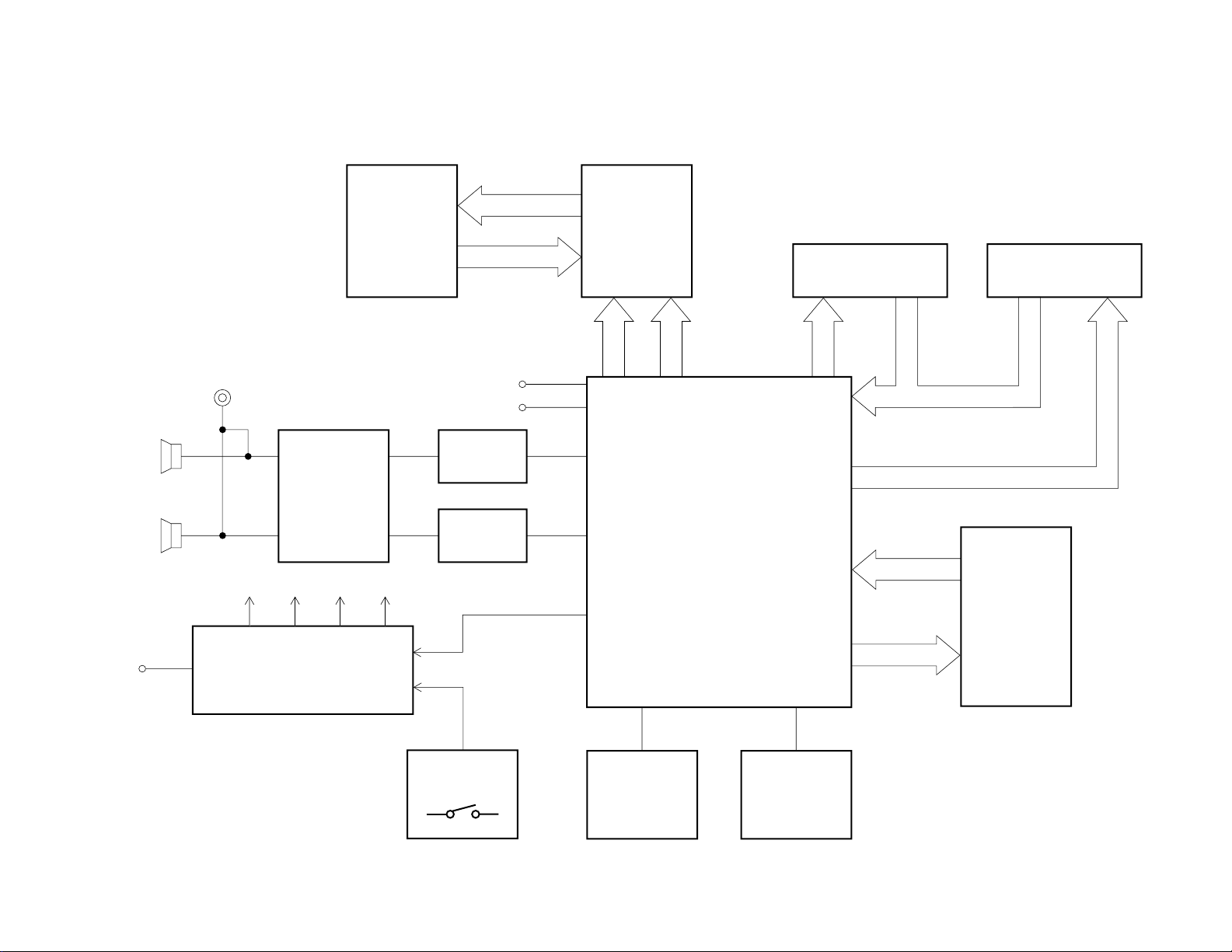
— 3 —
CPU
GT913F(T)
LSI1
Keyboard
Buttons
LCD
LCD Driver
KS0066U-10B
LSI3
Reset IC
UPD6379GR-E1
IC1
Oscillator
X1, Q1
Power Supply Circuit
Q201 ~ Q203, Q207, Q208, D205
Power Amp.
TA8248K
IC201
Filter (L)
Q206
Filter (R)
Q205
Phone/Output
VC VCC DVDD
AVDD
APO
DC + 9V IN
DB4 ~ DB7
MIDI IN
MIDI OUT
COM1 ~ COM16
SEG1 ~ SEG40
RS
R/W
E
KI0,KI1
FI8~FI10
FI0 ~ FI7
KC0 ~ KC7
MD0 ~ MD15
MA0 ~ MA19
ROM(8M-bit)
MSM538002E-
N8GS - KDR1
LSI2
Power Switch
BLOCK DIAGRAM
Page 6
CIRCUIT DESCRIPTION
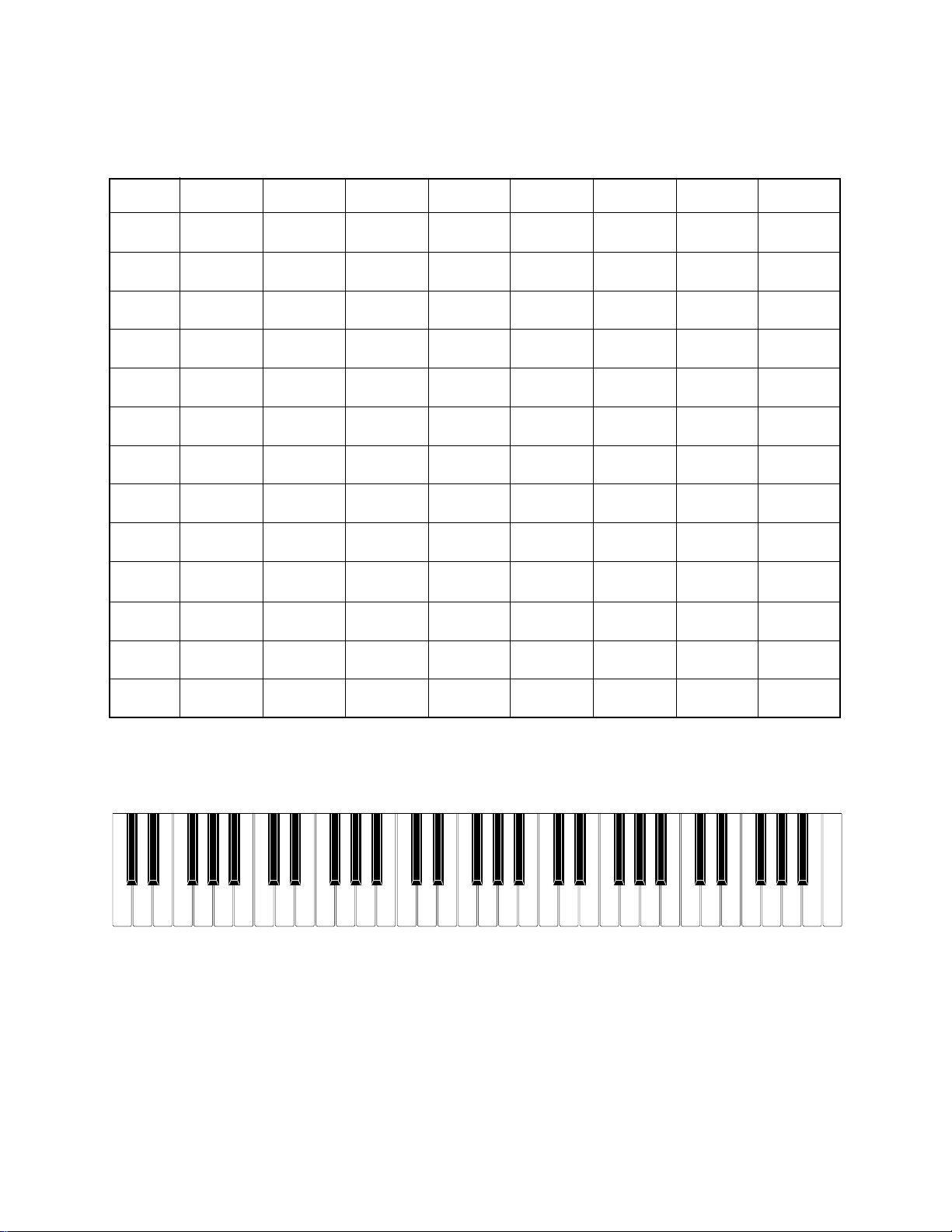
KEY MATRIX
KI0 KI1 KI2 KI3 KI4 KI5 KI6 KI7
KO0 C2 G#2 E3 C4 G#4 E5 C6 G#6
KO1 C#2 A2 F3 C#4 A4 F5 C#6 A6
KO2 D2 A#2 F#3 D4 A#4 F#5 D6 A#6
KO3 D#2 B2 G3 D#4 B4 G5 D#6 B6
KO4 E2 C3 G#3 E4 C5 G#5 E6 C7
KO5 F2 C#3 A3 F4 C#5 A5 F6
KO6 F#2 D3 A#3 F#4 D5 A#5 F#6
KO7 G2 D#3 B3 G4 D#5 B5 G6
KO8 —+0
KO9 321
KO10 6 5 4 Rhythm Tone
Tempo
Down
Start/
Stop
Transpose/
Tune/MIDI
KO11 9 8 7 Fingered Normal Off
KO12 FF Right Stop Left REW
Play/
Pause
Tempo
Up
Synchro/
Fill-In
Song
Bank
CASIO
Chord
Volume
Down
Chord
Book
Volume
Accomp
Volume
NOMENCLATURE OF KEYS
C#2
C2 D2E2F2G2A2 B2 C3 D3
F#2D#2
C#3A#2G#2
F#3 G#3
D#3
E3
F3 G3 A3 B3 C4 D4 E4 F4 G4 A4 B4 C5 D5 E5 F5 G5 A5 B5
A#3 C#4 D#4
F#4 G#4
A#4
C#5
D#5
F#5 G#5
A#5
C#6
C6
Up
G#6F#6D#6
A#6
B6A6G6F6E6D6
C7
— 4 —
Page 7
CPU (LSI1: GT-913F)
The 16-bit CPU contains a 1k-byte RAM, three 8-bit I/O ports, two timers, a key controller and serial interfaces.
The CPU detects key velocity by counting the time between first-key input signal FI and second-key SI from
the keyboard. The CPU reads sound data and velocity data from the sound source ROM in accordance with
the selected tone; the CPU can read rhythm data simultaneously when a rhythm pattern is selected. Then the
CPU provides 16-bit serial sound data to the DSP. The CPU also controls MIDI input/output and stores
sequencer data into the working storage RAM.
The following table shows the pin functions of LSI1.
Pin No. Terminal In/Out Function
1 TXD0 Out MIDI signal output
2 RXD0 In MIDI signal input
3 SCK0 Out APO (Auto Power Off) signal output
4, 5
6 SCK1 Out 1 MHZ synchronizing pulse output
7 AVCC In CVDD (+5 V) source
8 AN0 In +5 V when the keyboard is powered by batteries and becomes 0 V
9 AN1 In Input from pitch bender
10 AGND In Ground (0 V) source
11 BCK Out Bit clock output
12 SO Out Serial sound data output
13 LRCK Out Word clock output
14 GND In Ground (0 V) source
15, 16 XLT0, XLT1 In/Out 30 MHz clock input/output
17 VCC In +5 V source
18, 19 MOD0, MOD1 In Mode selection terminal
20 RSTB In Reset signal input
21 NMI In Power ON signal input
22 INT/P10 In/Out Data bus for the LCD driver
TXD/P13,
RXD/P14
In/Out Data bus for the LCD driver
AC adaptor detection terminal.
to cancel the APO function when AC adaptor is connected.
23 ~ 30
31 ~ 38 KC0 ~ KC7 Out Terminal for key scan signal
39 ~ 50
51 FI10 In Terminal for button input signal
52 SI10/P23 Out Chip enable signal for the LCD driver
53 ~ 55 KI0 ~ KI2 In Terminal for button input signal
56 MWNB Out Write enable signal for the DSP
57 ~ 76 MA0 ~ MA19 Out Address bus
77 MCSB0 Out Chip enable signal output for the sound source ROM
78 MCSB1 Out Not used
79 MCSB2 Out Chip enable signal output for the DSP
FI0 ~ FI3
SI0 ~ SI3
FI4 ~ FI9
SI4 ~ SI9
In Terminal for key input signal
In Terminal for key input signal
— 5 —
Page 8
Pin No. Terminal In/Out Function
80 VCC In +5 V source
81 GND In Ground (0 V) source
82 MRDB Out Read enable signal output for the sound source ROM
83 ~ 98 MD0 ~ MD15 In/Out Data bus
99 PLE Out Reset signal output for the DSP
100 P17 In/Out Data bus for the LCD driver
LCD DRIVER (LSI3: KS0066U-10B)
The LCD driver can drive a dot matrix LCD having 40 segment and 16 common lines. The LSI contains 240
graphic symbols in the built-in character generator ROM, and stores 80 characters in the built-in display data
RAM. In accordance with command from the CPU, the LSI is capable of displaying up to 16 characters
simultaneously. The following table shows the pin functions of KS0066U-10B.
Pin No. Terminal In/Out Function
1 ~ 22,
63 ~ 80
23 VSS — GND (0 V) source
24, 25 OSC1, OSC2 In/Out
26 ~ 30 V1 ~ V5 In Those voltages are used for generating the stepped pulse of
31, 32 LP, XCLS — Not used
33 VDD In DVDD (+5 V) source
34, 35 FR, DO — Not used
36 RS In
37 R/W In Read/Write terminal. High: read, Low: write
38 E In High: enable, the writing is done at fall edge.
39 ~ 42 DB0 ~ DB3 — Not used. Connected to GND (0 V)
43 ~ 46 DB4 ~ DB7 In/Out Data bus
47 ~ 62 COM1 ~ COM16 Out Common signal/output
SEG1 ~ SEG40 Out Segment signal output
Terminals for the built-in clock pulse generator. The external
resistor connected determines the oscillation frequency.
LCD drive voltage input.
the LCD drive signals.
Data/command determination terminal.
High: data, Low: command
Chip enable signal.
Low: disenable
— 6 —
Page 9

FILTER BLOCK
Since the sound signals from the CPU is stepped waveforms, the filter block is added to smooth the waveforms.
Amp.
TA8248K
Filter
Block
POWER AMPLIFIER (IC201: TA8248K)
The power amplifier is a two-channel amplifier with standby switch.
The following table shows the pin function of IC201.
Pin No. Terminal In/Out Function
1 NC — Not used
2 B.S.2 — Terminal for a bootstrap capacitor
3 OUT2 Out Channel 2 output
4 VCC In +9 V source
5 OUT1 Out Channel 1 output
6 B.S.1 — Terminal for a bootstrap capacitor
7 Power GND In Ground (0 V) source
8 Stand by In Power control signal input. 0 V: Off, +9 V: On
9 DC — Terminal for a decoupling capacitor
10 NF1 In Negative feedback input
11 IN1 In Channel 1 input
12 IN2 In Channel 2 input
13 NF2 In Negative feedback input
14, 15 Pre GND In Ground (0 V) source
CPU
MSM6755B-17
— 7 —
Page 10

MAIN PCB
1) Items to be adjusted:
ADJUSTMENT
Item
Vop voltage setting Voltmeter
2) Adjustment and Test Point Locations
Measuring Instrument
(TOP VIEW)
(BOTTOM VIEW)
Test point
VR1
— 8 —
Page 11

3) Equipment connection/Procedure
Vop voltage setting
Set Voltmeter
Output
CP3-CP4
Input
Connection
50°
LCD
Input
Point
Eye
Input
Signal
Adjust
Output
Connection
VR1 Voltmeter CP3-CP4
Output
Point
Adjust for
Adjust for 3.90 ~ 4.00V reading on voltmeter under the
temparature 20 ~ 25 °C.
Make fine adjustment according to the following instruction.
Watching the LCD at a 50° angle to the horizontal, adjust Vop
voltage so that unenergized segments are seen dimly.
— 9 —
Page 12

MAJOR WAVEFORMS
1
1 Clock pulse
GT913F(T) pin 15
4
5
2
3
2 Power source CVDD
JD connector pin 13
3 APO signal
JD connector pin 12
6
7
4 Sound waveform (R-ch) Tone: Whistle (59)
JD connector pin 6 Key: A4
5 Sound waveform (L-ch) Volume: Max.
JD connector pin 5
8
9
8 LCD common signal COM6
KS0066U-10B pin 52
9 LCD common signal COM7
KS0066U-10B pin 53
6 JB connector pin 1
7 JB connector pin 2
— 10 —
Page 13

PRINTED CIRCUIT BOARDS
Main PCB JCM456-MA1M
1 7 8
6
5
4
3
2
Main PCB JCM456-MA1M
Top View
6
Bottom View
— 11 —
Page 14

Sub PCB JCM453-MA2M
Sub PCB JCM453-MA2M
Top View
Bottom View
— 12 —
Page 15

Console PCB JCM453-CN1
Console PCB JCM453-CN1
Top View
Bottom View
— 13 —
Page 16

Keyboard PCB JCM618T-KY1M
Keyboard PCB JCM618T-KY1M
Top View
Keyboard PCB JCM618T-KY2M
Keyboard PCB JCM618T-KY2M
Bottom View
Top View
Bottom View
— 14 —
Page 17

Main PCB JCM456-MA1M
SCHEMATIC DIAGRAMS
5
3
2
4
8
9
6
1
7
— 15 —
Page 18

Sub PCB KDM453-MA2M
— 16 —
Page 19

Console PCBs JCM453-CN1
— 17 —
Page 20

Keyboard PCBs JCM618T-KY1M / KY2M
— 18 —
Page 21

22
33
14
15
29
28
26
27
24
25
30
23
14
15
37
16
3
7
6
9
8
13
34
5
4
12
38
4
20
20
19
21
18
35
21
17
2
1
´
9
3´8
´
10
´
18
R-4
R-4
R-1
15
34
31
36
32
R-5
R-3
R-2
10
10
34
34
11
37
EXPLODED VIEW
— 19 —
Page 22

PARTS LIST
CTK-541
Notes: This parts list does not include the cosmetic parts, which
parts are marked with item No. "R-X" in the exploded
view.
Contact our spare parts department if you need these
parts for refurbish.
1. Prices and specifications are subject to change without prior notice.
2. As for spare parts order and supply, refer to the
"GUIDEBOOK for Spare parts Supply", published
seperately.
3. The numbers in item column correspond to the same
numbers in drawing.
— 20 —
Page 23

PARTS PRICE LIST
CTK-541
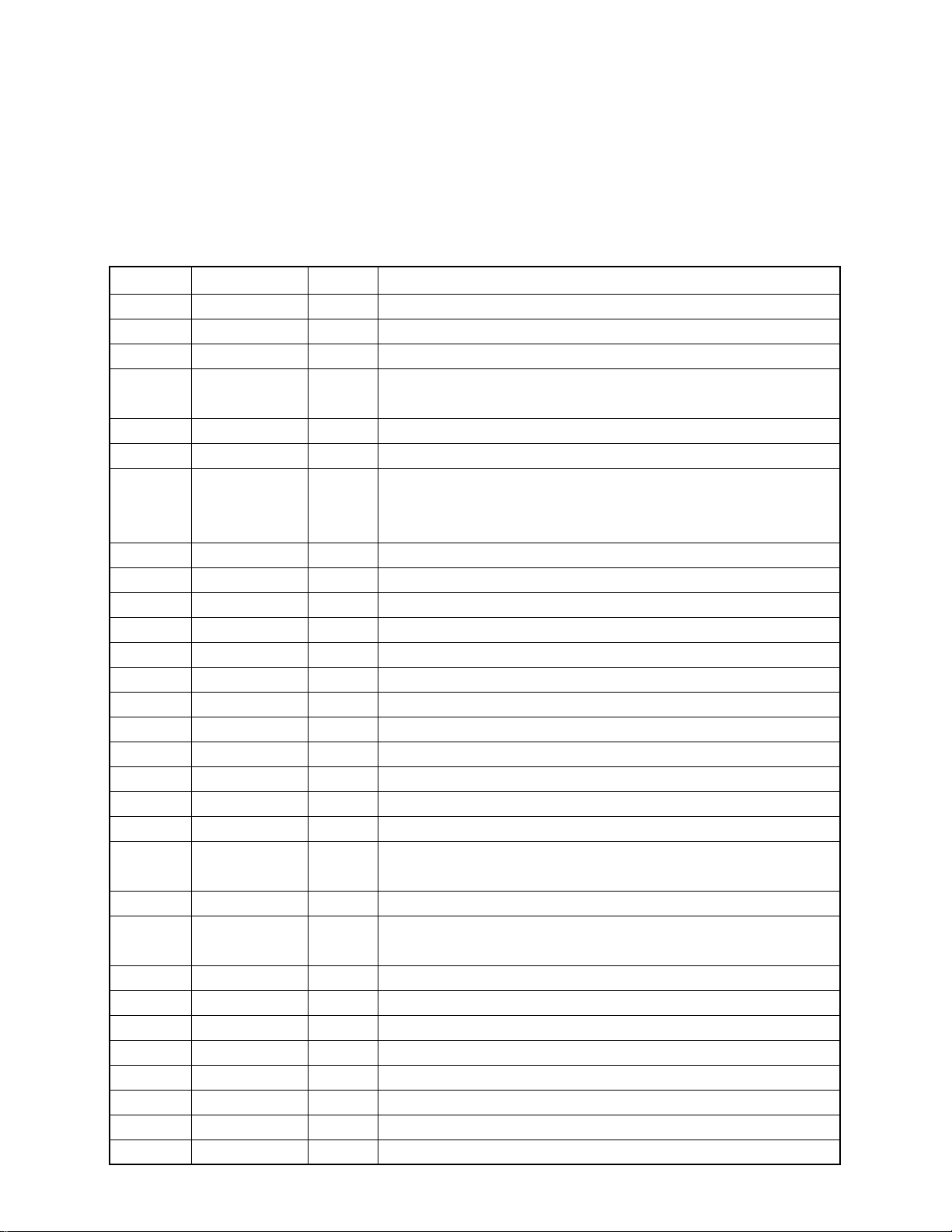
N Item Code No. Part Name Specification Q PRICE CODE R
Main PCB
N 1 6928 2120 PCB/ASSY (MA1M) M241173*1 1 DE B
D1-D4 2775 2079 DIODE/CHIP DA227TL 4 AA C
LSI1 2012 5005 LSI GT913F(T) 1 BO A
N LSI2 2012 6501 LSI/MC MSM538002E-S1GS-KDR1 1 AV A
LSI3 2012 5935 LSI/LCD DRIVER KS0066U-10B 1 AV A
IC1 2105 4746 LSI UPD6379GR-E1 1 AO B
IC2 2012 1883 IC/MOS RN5VD40AA-TR 1 AE B
Q1,Q2 2253 0308 TRANSISTOR 2SD1119-R(TX) 2 AC B
Q3 2250 1169 TRANSISTOR 2SA1576AT106R 1 AA B
Q4,Q7,Q8,Q11 2252 0637 TRANSISTOR 2SC4081T106R 4 AA B
VR1 2775 0994 POTENTIOMETER EVND8AA03B53 1 AA B
X1 2590 2774 OSCILLATOR/CERAMIC CSACV30.00MXJ040 1 AE B
SUB PCB ASS'Y
2 6927 3690 PCB/ASSY (MA2M) M140841*1 1 DB B
IC201 2114 5775 IC/LINEAR (POWER AMP) TA8248K 1 BI A
IC202 2114 1421 IC/PHOTO COUPLER PC900V 1 AK B
Q201,Q203 2250 1595 TRANSISTOR 2SB1240TV2R 2 AB B
Q205 2251 0672 TRANSISTOR 2SB1548-P.CS 1 AD B
Q202, Q204,
Q206-Q210
D201, D202 2390 3021 DIODE SRT14 2 AF B
D203, D205,
D207-D210
D206 2360 2044 DIODE/ZENER MTZJ6.2A-T77-T 1 AA C
D204 2360 1939 DIODE/ZENER MTZJ5.1C-T77-T 1 AA A
J201 3501 7049 JACK (POWER) HEC2305-01-330 1 AC A
J202 3612 0665 JACK (PHONE) YKB21-5006 1 AG B
J203 3612 0789 JACK YKB21-5010 1 AC B
J204 3501 4816 JACK/DIN YKF51-5051 1 AH B
N 3 6928 2130 PCB/ASSY (CN1M) M241172*1 1 BP C
LED301 2370 1414 LED MPR3338S-B149 1 AA B
N 4 6928 4500 PCB/ASSY (KY1M) M140687*5 1 BG B
D501 - D564 2301 0101 DIODE 1S2473T-77-T 64 AA B
N 5 6928 4510 PCB/ASSY (KY2M) M140688*5 1 BE B
D565 - D622 2301 0101 DIODE 1S2473T-77-T 58 AA B
6 6922 2720 KEY SET/LT WHITE M312118*1 4 AP A
7 6922 2730 KEY SET/LT WHITE M312118*2 1 AR A
8 6906 8481 KEY SET/LT BLACK 10P M140369A-3 2 AL A
9 6906 8591 KEY SET/LT BLACK 5P M140369A-4 1 AT A
N 10 5860 0679 SCREW 3X8 19 AA C
11 1909 2637 SCREW 3X18 21 AA C
12 6922 2762 RUBBER/CONTACT M211704B-1 4 AF A
13 6922 2772 RUBBER/CONTACT M211705B-1 1 AF A
2250 1592 TRANSISTOR 2SC1740STPR 7 AA B
2390 1344 DIODE 1SS133T-77-T 6 AA C
Console PCBs
Keyboard PCBs
Keyboard unit
- 21 -
Page 24

N Item Code No. Part Name Specification Q PRICE CODE R
R : Rank
Panel unit
14 3831 1096 SPEAKER S12J89A 2 BH B
15 1908 6418 SCREW 4X8 13 AA C
16 3335 6804 LCD LD-B10427E 1 BO B
17 6927 3890 RUBBER/INTERCONNECTOR M440759-1 2 AV B
18 6927 3920 REFLECTOR M240922-1 1 AM C
19 3122 3698 CFL HMBV4BG2W106NLUAZG 1 AX C
20 6927 3420 HOLDER/CFL M440758-1 2 AA C
N 21 6927 3900 PACKING
22 6921 5031 KNOB M311859A-1 1 AA B
23 6927 0510 SWITCH/SLIDE KNOB CSB-08D 1 AD B
24 6927 3820 RUBBER/BUTTON M140821-1 1 AI B
25 6927 3830 RUBBER/BUTTON M240928-1 1 AD B
26 6927 3840 RUBBER/BUTTON M240929-1 1 AD B
27 6927 3850 RUBBER/BUTTON M140824-1 1 AG B
28 6927 3860 RUBBER/BUTTON M240931-1 1 AC B
29 6927 3870 RUBBER/BUTTON M240932-1 1 AK B
30 6903 2150 RUBBER/BUTTON M341091-1 1 AA B
31 6903 2150 SPRING/BATTERY(+) M41330-1 1 AA B
32 6902 6141 SPRING/BATTERY(-) M41226A-1 1 AB B
N 33 6928 4910 PLATE/DISPLAY M241161-1 1 AW C
34 5111 5163 SCREW 4X10 40 AA C
N 35 5860 0679 SCREW 3X8 18 AA C
N 36 5150 1640 SCREW 3X10 10 AA C
N 37 5161 3171 SCREW 4X12 8 AA C
38 6906 9218 COVER/BATTERY M311164H*17 1 AW B
Accessory
6906 9043 STAND/NOTE M340701*2 1 BK B
M440760-1
2 AC C
Notes: Q : Quantity
- 22 -
Page 25

CASIO TECHNO CO.,LTD.
Overseas Service Division
Nishi-Shinjuku Kimuraya Bldg. 1F
5-25, Nishi-Shinjuku 7-Chome
Shinjuku-ku, Tokyo 160-0023, Japan
 Loading...