


SERVICE MANUAL

REFERENCE MANUAL
Oct. 1999
Table of content
Page
1 1. PRODUCT OUTLINE
12. CHANGES FROM THE BJC-80/80v
13. EXTERNAL APPEARANCE
24. SPECIFICATIONS
24.1 PRINTER SPECIFICATIONS
34.2 INTERFACE SPECIFICATIONS
64.3 PAPER SPECIFICATIONS
74.4 PHOTO BJ CARTRIDGE SPECIFICATIONS
85. OPERATION
8 |
5-1. FUNCTION SETTING |
105.2 ERROR INDICATIONS
115-3. INK LOW WARNING RESET BY BUTTON OPERATION
125-4. DIRECT PRINTING FUNCTION OF THE IMAGE FROM DIGITAL CAMERAS
136. SPECIAL TOOLS
147. PARTS LIST
158. CIRCUIT DIAGRAM
1. PRODUCT OUTLINE
The BJ M70 and the BJC-85 are portable, color BJ printers targeting the personal use market. As successive models of the BJC-80/80v, the following functions have been added, the ease of connection has been improved, and the functions as a portable spacesaving printer has been strengthened.
(1)The high-speed IrDA (Ver.1.1) enables the printer to attain print speed comparable to that of the Centronics interface.
(2)Direct printing from digital cameras by the new standards of IrTran-P.
(3)Support of the USB I/F function.
(4)Photo printing function is added.
2. CHANGES FROM THE BJC-80/80v
1)New adoption of the photo cartridge (Photo printing function is added.)
2)The IrDA version upgrade from Ver. 1.0 to 1.1 has enabled faster transmission.
3)New adoption of IrTranP (Direct printing from digital cameras, enabled only in BJ M70).
4)New adoption of USB I/F
5)One emulation (BJC-85: LQ mode / BJ M70: BJ mode)
6)Button reset of the ink low warning is added.
7)Various specifications / Circuit diagram
8)Special tool (spur cleaner) is added.
3. EXTERNAL APPEARANCE
The BJ M70 and the BJC-85 have the same appearance as the BJC-80/80v, except for the following:
(1)The USB I/F connector has been added to the right side of the printer.
(2)The color of the panel cover and inner cover has been changed from gray to blue.
USB Connector
Changed from gray to blue.
1
4. SPECIFICATIONS
4-1. PRIINTER SPECIFICATIONS
Type |
Portable serial color bubble jet printer |
||
Paper feeding |
Auto sheet feed |
|
|
method |
|
|
|
Printing speed |
Burst HS: 434cps HQ: 346cps (when using the BC-10) |
||
|
Throughput: |
|
|
|
BC-10 |
|
|
|
New monochrome pattern (E) |
5 ppm(HS) 3.9 ppm(Standard) |
|
|
New monochrome pattern (J) |
5 ppm(HS) 4.3 ppm(Standard) |
|
|
BC-11e |
|
|
|
New color pattern (E) |
2 ppm(HS) 1.6 ppm(Standard) |
|
|
New color pattern (J) |
2 ppm(HS) 1.7 ppm(Standard) |
|
|
BC-12e |
|
|
|
A4 full address |
1.0ppm (HQ) |
|
|
|
||
Printing direction |
Unidirectional (automatically selected according to the print data) |
||
|
|
|
|
Max. Print Width |
203 mm |
|
|
Line feed pitch |
136 ms/line (128" /360" line feed) |
||
|
|
|
|
Built-in print |
LQ mode: BJC-85 only |
|
|
control mode |
BJ mode: BJ M70 only |
|
|
|
Native mode |
|
|
|
BJL command |
|
|
|
|
|
|
Detection functions |
Presence of paper: Available |
|
|
|
Presence of BJ cartridge: Available |
||
|
Waste ink amount: Available |
|
|
|
Paper width: Not available |
|
|
|
Distinction of BJ cartridge: Available |
||
|
Ink low: Available (by using the dot-count) |
||
Noise |
Sound pressure level: conforms to ISO9296 |
||
|
Approx. 45 dB (A) or less during operation (HQ/HS mode) |
||
Environmental |
During operation |
Temperature 5oC to 35oC (41oF to 95oF) |
|
requirements |
|
Humidity |
10%RH to 90%RH (no condensation) |
|
Non operation |
Temperature 0oC to 35oC (32oF to 95oF) |
|
|
|
Humidity |
5%RH to 95%RH (no condensation) |
Power supply |
Input voltage/Frequency: |
|
|
|
AC100 V, 50/60 Hz AC120 V, 60 Hz AC230 V, 50 Hz AC240 V, 50 Hz |
||
|
Power consumption |
|
|
|
Printing status |
Standby status |
Soft power off |
|
Max. 30 W |
3 W |
2 W |
External |
300 mm (W) x 157.6 mm (D) x 57 mm (H) |
||
dimensions |
|
|
|
Weight |
Approx. 1.4 Kg (including BJ cartridge) |
||
|
|
|
|
2
4-2. INTERFACE SPECIFICATIONS
The interface specifications of this printer is shown below.
1)Bidirectional Centronics Interface (IEEE1284 compatible)
2)Infrared Interface
IrDA Interface Ver. 1.1 / IrTranP
ASK Interface
3)USB Interface
<Difference from the BJC-80/80v>
1)The specified version of IrDA is changed from Ver. 1.0 to 1.1.
2)IrTranP compliant.
3)USB interface compliant.
IrDA Ver. 1.1 and USB I/F compliancy for preinstalled Windows 98 PCs. Windows 95 PCs comply with IrDA Ver. 1.0.
The specifications of IrDA Ver. 1.1 and USB I/F are explained below. See the BJC-80/80v
Service Manual for details regarding the bidirectional interface/ASK interface.
4-2-1. IrDA Interface
1)Interface
IrDA Version 1.1 compatible
2)Optical specifications
|
Light generation |
|
|
Wavelength: |
0.85 to 0.90 µm |
|
Intensity: |
100 to 500 m W/Sr |
|
Light angle: |
±15o (along optical axis) |
|
Light interception |
|
|
Wavelength: |
0.85 to 0.90 µm |
|
Intensity: |
4µ W/cm2 to 500m W/cm2 |
|
|
10µ W/cm2 to 500m W/cm2 |
|
|
(when the communication speed is more than 0.576 MHz.) |
|
Light angle: |
Max. ±15o (along optical axis) |
3) |
Transfer speed |
9600/19200/38400/57600/115.2k/576k/1.152M/4M bps |
4) |
Communication |
Half duplex, start/stop system (bidirectional): |
|
method |
when the transfer speed is less than 115.2kbps |
|
|
Half duplex, frame synchronization system (bidirectional): |
|
|
when the transfer speed is more than 0.576Mbps |
5) |
Communication |
0 to 1m: when the transfer speed is less than 115.2kbps |
|
distance |
0 to 0.8m: when the transfer speed is more than 0.576Mbps |
3
6)Maximum received 2048 byte/packet data size
7)Modulation method 3/16 RZI (Return to Zero Invert):
|
|
when the transfer speed is less than 115.2kbps |
|
|||||
|
|
1/4 RZI (Return to Zero Invert): |
|
|||||
|
|
when the transfer speed is 0.576Mbps and 1.152Mbps |
|
|||||
|
|
4 PPM (Pulse Position Modulation): |
|
|||||
|
|
when the transfer speed is 4Mbps |
|
|||||
4-2-2. USB Interface |
|
|
|
|
|
|
|
|
<Specifications> |
|
|
|
|
|
|
|
|
1) |
Device structure |
Self-powered device |
|
|
|
|
|
|
2) |
Data transfer |
Half duplex serial interface |
|
|
|
|
|
|
|
method |
Universal Serial Bus Specification Revision 1.0 compatible |
|
|||||
|
|
Universal Serial Bus Device Class Definition for printing |
|
|||||
|
|
Device Version 1.0 compatible |
|
|||||
|
|
Signal rate: 12Mbps (full speed) |
|
|||||
|
|
Transfer type: Control transfer/Bulk transfer |
|
|||||
3) |
Input/output circuit |
No. |
Signal name |
2 |
|
|
|
1 |
|
|
1 |
Vcc |
|
|
|
||
|
|
|
|
|
|
|
||
|
|
2 |
-Data |
Data signal line |
|
|
|
|
|
|
|
|
|
|
|||
|
|
3 |
+Data |
Data signal line |
|
|
|
|
|
|
|
|
|
|
|||
|
|
4 |
GND |
|
|
|
|
|
|
|
|
|
|
|
|
||
|
|
|
|
3 |
|
|
|
4 |
|
|
|
|
Series B |
|
|||
<Signal level>
Vcc: "H" level input voltage: +2.0V to +5.5V "L" level input voltage: +0.0V to +0.8V
-Data, +Data: Differential input sensitivity
"H" level input voltage: +2.8V to +3.6V
"L" level input voltage: +0.0V to +0.3V
4) Interface cable Material: AWG No.28 or larger
Full speed device cable (with twisted-pair shield)
Less than 5 mm
5)Interface connector Printer-side: USB standard, Series B receptacle
Cable-side: USB standard, Series B plug
4
<Technical explanation>
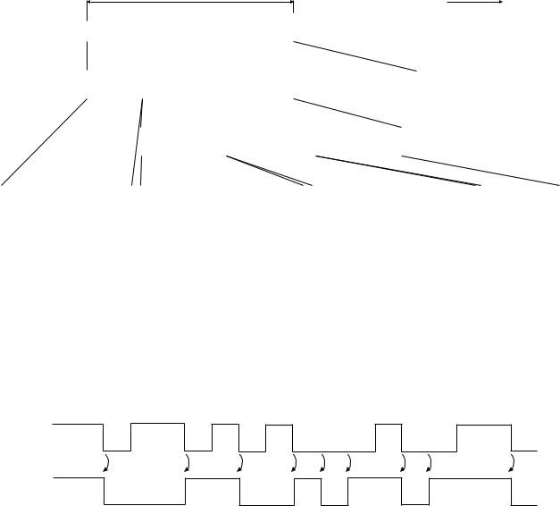
USB is a serial interface which connects up to 127 peripheral devices to a host computer, and transmits data at a high-speed rate of 12Mbps. Hot plugging, in which connecting/disconnecting devices while the host or the printer is in use, is supported. Each device is connected to a hub's port, where each port's detection/disconnection status is returned to the host.
Data transfer
The data transfer in USB is executed in terms of the transfer unit called a frame, a time frame of approximately 1ms, into which the data is divided. Data is transferred by piling up these frames.
All packets begin with a SYNC (synchronizing) field to synchronize with the local clock, and are separated with an EOP (End of Packet) field.
Frame lines begin with an SOF (Start of Frame) packet. An SOF is composed of a PID (Packet Identification Field) that represents the type of the packet and the direction, frame number, and a CRC (Cyclic Redundancy Check) used for error-check.
Inside a frame is a packet line containing a token packet, data packet and a handshake packet, which indicates the status of the flow control.
A token packet is composed of a PID, an address field which can specify up to 128 addresses, an ENDP (endpoint) field, and a CRC.
Inside a data packet are a PID, data field, CRC, and EOP.
Only a PID is present inside the handshake packet.
1 frame (Approx.1ms) Time passage
Frame line |
SOF |
|
SOF |
|
|
|
|
|
|
Frame inside |
|
SOF |
|
|
Printer |
|
|
|
|
Other functions |
|
|
|
|
|
|
|
|
|
||||||||
|
|
|
|
|
|
|
|
|
|
|
|
|
|
|
|
|
|
|
|
|
|
|
|
|
|
|
|
|
|
Packet line |
|
|
|
|
|
|
|
|
|
|
|
|
|
|
|
|
|
|
|
|
|
||||
|
|
Token |
|
Data |
|
|
Handshake` |
|
|
|
|
|
|
|
|
|
|||||||||||
Packet inside |
|
|
|
|
|
|
|
|
|
|
|
|
|
|
|
|
|
|
|
|
|
|
|||||
|
|
|
|
|
|
|
|
|
|
|
|
|
|
|
|
|
|
|
|
|
|
||||||
|
|
|
|
|
|
|
|
|
|
|
|
|
|
|
|
|
|
|
|
|
|
|
|
|
|
|
|
SYNC |
Frame |
CRC |
EOP |
|
SYNC |
PID |
ADDR |
|
ENDP |
CRC |
EOP |
|
|
SYNC |
PID |
|
DATA |
|
CRC |
EOP |
|
SYNC |
PID |
EOP |
|||
Nunber |
|
|
|
|
|
|
|
||||||||||||||||||||
|
|
|
|
|
|
|
|
|
|
|
|
|
|
|
|
|
|
|
|
|
|
|
|
|
|
|
|
|
|
|
|
|
|
|
|
|
|
|
|
|
|
|
|
|
|
|
|
|
|
|
|
|
|
|
|
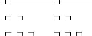
Encoding/Decoding the Data
In USB, data transfer lines are ultimately encoded with NRZI (Non Return to Zero Invert) method. When the original data bit is 0, sent data bits are inverted; when the original data bit is 1, the value is retained.
However, if the level of the transferred data remain unchanged for a certain period of time, the receiving side may not be able to synchronize with the data sample position, which will result in data bits being out of phase. This is prevented by a method called bit stuffing; when data bit 1 is repeated 6 times, one 0 bit is added to the original data before encoding with NRZI.
0 |
1 |
1 |
0 |
1 |
0 |
1 |
0 |
0 |
0 |
1 |
0 |
0 |
1 |
1 |
0 |
Data
Idle
NRZI
Idle
5

4-3. PAPER SPECIFICATIONS
Plain paper (Weight: 64 to 90g / m2)
Government postcard (Weight: 90g / m2, Thickness: 0.23 mm) Coated paper (Canon coated paper LC-301, A4/LTR)
High resolution paper (Canon high resolution paper HR-101, A4/LTR) Glossy paper (Canon glossy paper GP-301, A4/LTR)
Transparency film (Canon transparency film CF-102, A4/LTR) BPF (Canon back print film BF-102, A4/LTR)
Glossy film (Canon glossy film HG-101, A4/LTR)
T-shirt transfer (Canon T-shirt transfer TR-201, A4/LTR)
Fabric sheet (Canon fabric sheet FS-101, A4/LTR)
Glossy postcard (Canon glossy postcard KH-201)
Photo glossy postcard (Canon photo glossy postcard FM-101) Envelope (Size 4, size 6, COM #10, DL)
Note: Printing on fanfold paper and labels is not supported.
|
Type |
Paper |
Size |
Remarks |
|
|
Plain paper*1 |
PB (SK/DK) |
A4, B5, A5 |
Suggested paper |
|
|
|
Kangas |
A4 |
|
|
|
|
Neusiedler |
A4 |
See *1 |
|
|
|
Boise Cascade |
LTR, LGL |
|
|
|
|
XX4024(75g/m2) |
LTR, LGL |
|
|
|
|
XX4024(95g/m2) |
LTR, LGL |
|
|
|
|
Fox River Bond |
LTR |
|
|
|
Color BJ plain paper |
LC-301 |
A4, LTR |
See *1 |
|
|
High resolution paper*2 |
HR-101 |
A4, LTR |
See *2 |
|
|
Glossy paper*2 |
GP-301 |
A4, LTR |
See *2 |
|
|
Transparency film*2 |
CF-102 |
A4, LTR |
See *2, Note 1)&2) |
|
|
BPF*3 |
BF-102 |
A4, LTR |
See *3, Note 2) |
|
|
Glossy film*2 |
HG-101 |
A4, LTR |
See *2, Note 2 |
|
|
T-shirt transfer |
TR-201 |
A4, LTR |
See *3 |
|
|
Fabric sheet*3 |
FS-101 |
A4, LTR |
See *3, Note 1) |
|
|
Government postcard*2 |
---------- |
100 x 148* |
See *2 |
|
|
Glossy postcard*2 |
KH-201 |
100 x 148* |
See *2 |
|
|
Photo glossy postcard |
FM-101 |
215.9 x 119.6* |
See *3 |
|
|
Envelope*4 |
Size 4 |
235 x 105* |
See *4 |
|
|
|
Size 6 |
190 x 98* |
|
|
|
|
COM #10 |
241 x 106* |
|
|
|
|
DL |
220 x 110* |
|
|
|
Thick paper |
91 to 105g / m2 |
|
|
|
*: Unit: mm
*1:Stackable up to 3 mm (Approx. 30 sheets). For legal size paper, feeds single sheet. *2: Stackable up to 10 sheets *3: Single paper feeding *4: Stackable up to 5 sheets
Note 1): A plain sheet of paper should be set under the back print film, fabric sheet, and T- shirt transfer.
Note 2) Transparency film, back print film, and Glossy film are usable when the humidity is 70 % or less.
6

4-4. PHOTO BJ CARTRIDGE SPECIFICATIONS
Photo cartridge BC-12e
BJ cartridge BC-12e: Ink cartridge replaceable type of color BJ cartridge (drop modulation adopted)
Ink cartridge BCI-12Bk: Black (64 nozzles)
Ink cartridge BCI-12Color: Yellow, Magenta, Cyan (24 nozzles x 3)
No. of pages printed |
Approx. 20 pages : reference value |
|
(in the HR-Fine mode, 7.5% duty pattern per color (A4) |
|
: calculated value) |
Weight |
Approx. 29 g (including both ink cartridges) |
Print speed |
Approx. 0.1 pp : reference value |
|
(A4 full address printing pattern) |
Nozzle check pattern |
Same as the BC-11e |
HR-Fine mode |
|
Carriage motion: |
3 pass |
Printing nozzle: |
8 nozzle |
Resolution: |
360 dpi |
Carriage driving frequency: |
5.00 kHz |
Photo print mode can be used to obtain high level gradation print quality when using the Photo BJ cartridge. These cartridges contain light density ink which achieves a rich gradation and reduced graininess by printing several times over the same dot.
The printer driver divides the pixel data into a maximum of 4-values (not printed, print 1 dot, print 2 dots and print 3 dots) enabling each pixel to be printed in up to 4 gradations. The printer therefore makes three passes using a maximum of 150% more ink than usual. This Photo cartridge adopts drop modulation, decreasing granularity of the light density parts by efficiently ejecting large and small ink droplets.
Head ID
|
|
Carriage ribbon cable contact part pin No. / Signal name |
||||
Head |
|
11/ID0 |
12/ID1 |
13/HCONT |
||
|
BC-10 |
L |
L |
|
H |
|
|
BC-11e |
H |
L |
|
L |
|
|
BC-12e |
H |
H |
|
L |
|
|
No head installation error |
H |
H |
|
|
|
|
|
|
|
|||
The printer has no detection function of the ink cartridge type, and for the BC-11e and BC12e, the ink cartridges to be installed are not incompatible, therefore, the following mistaken installation may occur. In case the BCI-12 Bk/Color are installed in the print head of the BC11e, as the printer recognizes that the color cartridge (BC-11e) has been installed in spite of light density photo ink cartridge installation, low density imaging is produced. In case of the installation of the BCI-11 Bk/Color in the print head of the BC-12e, in reverse, high density colored imaging is produced.
7
5. OPERATION
5-1. FUNCTION SETTING
Default setting
The default setting can be set by button operation when the power is turned on. When the printer is turned on, hold down the POWER button until the beeper sounds the specified number of times for the desired function setting, and release the POWER button to set.
Function Setting
|
Mode |
Beeper |
Remark |
|
|
|
|
|
Table 1 |
7 times |
Factory default setting |
|
Table 2 |
8 times |
|
|
Table 3 |
9 times |
|
|
Table 4 |
10 times |
|
|
Table 5 |
11 times |
|
<Difference from the BJC-80> BJC-85
1)No setting regarding the BJ mode
2)The setting to enable/disable the ink low warning is added.
3)The setting of Euro font is added.
|
Table 1 |
Table 2 |
Table 3 |
Table 4 |
Table 5 |
|
Print mode |
HQ |
HQ |
HQ |
HQ |
HQ |
|
Left margin |
LTR |
LTR |
A4 |
A4 |
A4 |
|
Text scale mode |
Disable |
Disable |
Disable |
Disable |
Disable |
|
Paper feed position |
8.5 mm |
8.5 mm |
8.5 mm |
8.5 mm |
8.5 mm |
|
Smoothing |
Disable |
Disable |
Disable |
Disable |
Disable |
|
Reduction |
1/1 |
1/1 |
1/1 |
1/1 |
1/1 |
|
Automatic power off |
Disable |
Disable |
Disable |
Disable |
Disable |
|
Font |
Roman |
Roman |
Roman |
Roman |
Roman |
|
Font lock |
Disable |
Disable |
Disable |
Disable |
Disable |
|
Input/download buffer |
25 kB/0 kB |
25 kB/0 kB |
25 kB/0 kB |
25 kB/0 kB |
25 kB/0 kB |
|
Automatic line feed |
CR |
CR |
CR |
CR |
CR |
|
International character set |
USA |
USA |
USA |
USA |
USA |
|
Character set |
Italics |
Italics |
Italics |
Italics |
Graphics |
|
Code page |
437 |
437 |
437 |
437 |
858 |
|
Ink low warning |
Disable |
Enable |
Disable |
Disable |
Disable |
|
|
|
|
|
|
|
|
When the printer is turned on, hold down the POWER button until the beeper sounds 12 times to change "Code Page" in the following table to "858," "Character Set" to"Graphics." Other items will not be changed.
8
<Difference from the BJC-80v> BJ M70
1)No setting regarding the LQ mode
2)The setting to enable/disable the ink low warning is added.
|
Table 1 |
Table 2 |
Table 3 |
Table 4 |
Table 5 |
|
Operation mode change |
BJ |
BJ |
|
|
|
|
Print mode |
HQ |
HQ |
|
|
|
|
Automatic power off |
Disable |
Disable |
|
|
|
|
Smoothing |
Disable |
Disable |
|
|
|
|
Remaining ink |
Disable |
Enable |
Same as |
Same as |
Same as |
|
Reduction |
1/1 |
1/1 |
Table 1 |
Table 1 |
Table 1 |
|
BJ Paper feed position |
8.5 mm |
8.5 mm |
|
|
|
|
BJ receive buffer |
23 kB |
23 kB |
|
|
|
|
BJ ANK character quality |
Normal |
Normal |
|
|
|
|
BJ ANK character set |
Katakana |
Katakana |
|
|
|
|
BJ CR function (+LF) |
CR only |
CR only |
|
|
|
|
BJ ANK international |
Japan |
Japan |
|
|
|
|
character |
|
|
|
|
|
|
9

5-2. ERROR INDICATIONS
<Difference from the BJC-80/80v>
|
Beeper |
|
|
|
BJC-80/80v |
BJC-85/BJ M70 |
|
Waste ink warning |
4 times |
5 times |
|
Low battery warning |
3 times |
4 times |
|
Ink low warning |
Once |
Twice |
|
Cartridge replacement compulsory |
Twice |
3 times |
|
completion warning |
|
|
|
Diode sensor error |
9 times |
------*1 |
|
*1: Eliminated
<BJC-85/BJ M70 error indications>
Error condition |
Error LED |
Power LED |
Beeper |
[Recoverable by customers] |
(Orange) |
(Green) |
|
Paper pick-up error |
Lights |
Lights |
Once |
Paper delivery error |
Lights |
Lights |
Twice |
BJ cartridge check |
Lights |
Lights |
3 times |
Cartridge mis-match |
Lights |
Lights |
4 times |
Ink low warning*1 |
Blinks |
Lights |
Twice |
Cartridge replacement compulsory |
Blinks |
Lights |
3 times |
completion warning |
|
|
|
Low battery warning |
Blinks |
Lights |
4 times |
Waste ink warning |
Blinks |
Lights |
5 times |
Low battery error (with battery) |
Blinks |
Blinks |
Long, then short |
|
|
|
|
[Unrecoverable by customers] |
|
|
|
ROM error |
Blinks |
Blinks |
Once |
RAM error |
Blinks |
Blinks |
Twice |
No head installation error |
Blinks |
Blinks |
3 times |
HP sensor error |
Blinks |
Blinks |
4 times |
Waste ink full error |
Blinks |
Blinks |
5 times |
Internal temperature error |
Blinks |
Blinks |
6 times |
Print position detection error |
Blinks |
Blinks |
7 times |
Abnormal temperature rise error |
Blinks |
Blinks |
8 times |
EEPROM error |
Blinks |
Blinks |
11 times |
Low battery error (with AC adapter) |
Blinks |
Blinks |
Long, then short |
|
|
|
|
*1: Ink low warning is enabled only when the ink low warning selection is set to on.
10
5-3. INK LOW WARNING RESET BY BUTTON OPERATION
Ink low warning
This printer detects the remaining ink level by counting the number of ejected ink dots in the same way as the BJC-80/80v. When the setting of the ink low warning is enabled, and the remaining ink gets low, the beeper sounds twice, and the ERROR LED blinks.
Pressing the cartridge replacement button will sound the beeper and move the carriage to the center, and the ERROR LED indicates the ink cartridge for which the remaining ink is low as shown below.
Blinks once: when the remaining ink of the BCI-10 / BCI-11Bk / BCI-12Bk is little
Blinks twice: when the remaining ink of the BCI-11Color / BCI-12Color is little
Blinks 3 times: when the remaining ink of the BCI-11 BK & Color / BCI-12 BK & Color is little
The ink low warning reset function by button operation is added to this printer. The button operation procedures are shown below. (The ink low warning of the BJC-80/80v can be reset from the host computer only.)
Operation
1)Turn on the printer.
2)Press the cartridge replacement button to move the carriage to the center.
If the carriage was moved to the center by signals from the PC, the reset operation by the cartridge replacement button is not possible.
3)Make sure that the proper cartridge is installed in the carriage. If not, install the proper one. (The ink dot counter reset is effective only to the ink cartridge type installed in the carriage.)
4)Press and hold the RESUME button for the number of beeps corresponding to the warned ink type to select the ink type for which the dot counter is to be reset, and release the RESUME button. The number of beeper sounds is as follows:
Once: |
The dot counter of the BCI-10/BCI-11Bk/BCI-12Bk is reset. |
Twice: |
The dot counter of the BCI-11Color/BCI-12 Color is reset. |
3 times: |
The dot counter of the BCI-11Bk&Color/BCI-12Bk&Color is reset. |
4 times: |
The selected ink type is canceled. |
5)Press the cartridge replacement button.
The ink dot counter selected in the procedure 4) and the ink low warning are reset, and at the same time, the carriage returns to the home position.
11
5-4. DIRECT PRINTING FUNCTION OF THE IMAGE FROM DIGITAL CAMERAS (BJ M70 only)
<Difference from the BJC-80/80v>
The new adoption of IrTranP has enabled the printing of data directly sent from digital cameras compliant to IrTranP standards, not through the host computer, but via IrDA communication.
Specifications |
|
Data communication form: |
IrTranP standards compatible |
Input image size: |
640 x 460 pixels |
Input image capacity: |
128 Kbyte or less |
Output image size: |
Landscape: 90 x 68 mm |
|
Portrait: 77 x 103 mm |
|
Seal printing: 19 x 26 mm x 16 images |
Paper size: |
Postcard |
Operation
<Image printing>
After receiving the data, the image data is output by pressing the RESUME button, and releasing before the beeper sounds. This is not effective when an error has occurred or paper is fed.
<Reprinting>
The image data is also maintained in the memory after printing, and will not be abandoned until new image data is received from the digital camera, or print data is input from the host computer. Reprinting of data is possible by pressing the RESUME button (and releasing before the beeper sounds).
<Printing cancellation>
During the printing of image data, printing is cancelled by pressing the RESUME button until the beeper sounds once, then releasing. In this case paper is delivered. The remaining data halfway through printing is abandoned. (As the image data has been maintained, it is possible to reprint the data, without resending the data from the digital camera.)
<Printing position definition>
To select the printing position, press the POWER button and cartridge replacement button simultaneously when the power is on, and release the buttons after the beeper sounds the number of times applicable to the printing position to be selected. This setting returns to the default (Landscape) by powering off. The number of beeper sounds is as follows:
Once: |
Portrait |
Twice: |
16-image seal printing |
3 times: |
Photo glossy card landscape |
4 times: |
Photo glossy card portrait |
5 times: |
Setting completed. (The power is normally turned on.) |
12
6. SPECIAL TOOLS
Clean spurs by using the spur cleaner in case spur marks are left on the print images.
Special tool (part number) |
Remarks |
Spur cleaner (QY9-0055-000) |
For cleaning spurs |
Usage
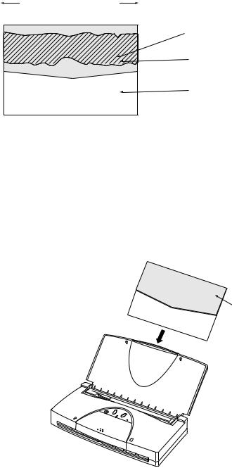
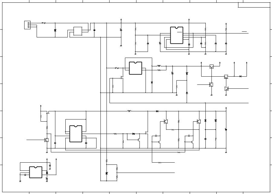
1)Moisten the fabric part of the spur cleaner with approx. 5 cc of water.
Moisten the fabric with the water, as shown below, so that the fabric absorbs the water from end to end.
Be careful not to moisten the fabric with too much water. In case too much water is used, there is the possibility that water will be wrung from the spur cleaner when passing through the paper feed roller, spread inside the printer, and cause failure.
Be careful that the water is absorbed by the fabric from end to end.
Part moistened with water
Fabric (white-colored)
Spur cleaner
Transparent film
2)Turn on the power of the printer. Remove the paper from the ASF to set the spur cleaner with the fabric-affixed part of the cleaner face-up and to the top.
3)Press the RESUME button, and release it after the beeper sounds once. The spur cleaner is fed and stops at the print start position.
4)Press the RESUME button again, and release it after the beeper sounds once. The spur cleaner is delivered. Repeat procedures 3) to 4) approx. 5 times in case of heavy soiling.
5)Set a single sheet of paper to the ASF to repeat procedures 3) and 4). (To remove the moisture remaining in the paper feeding path.)
Spur cleaner
Fabric (white-colored)
13

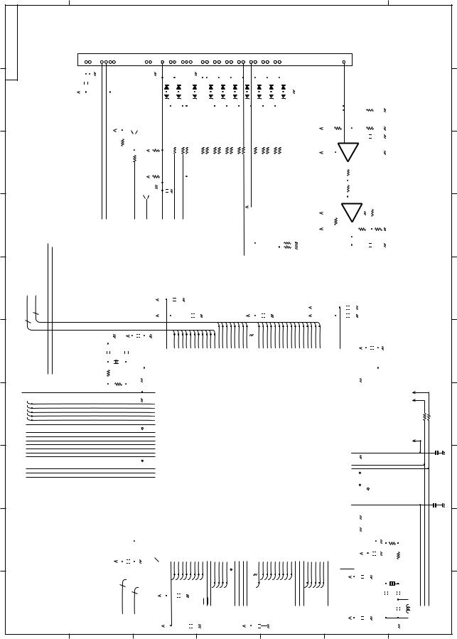
7. PARTS LIST
|
BJC-85 |
BJ M70 |
|
COVER, INNER |
QB1-4449 |
QB1-4450 |
|
COVER, PANEL |
QB1-4451 |
QB1-4452 |
|
CONTROL PCB ASS'Y |
QG2-3096 |
QG2-3097 |
|
CHASSIS PLATEN UNIT |
QG5-1476 |
QG5-1481 |
|
FLASH-ROM |
QH8-0258 |
QH8-0259 |
|
Service parts other than the above are common for BJC-85 and BJ M70. See the BJC-85 and BJ M70 Parts Catalog for details.
14
15
1 |
2 |
3 |
4 |
5 |
6 |
7 |
8 |
9 |
10 |
|
|
|
|
|
|
|
|
|
CONTROL PCB ASS'Y 01 |
|
DC connector |
|
|
|
|
|
|
|
A |
|
|
|
Vpp |
|
|
Vcc1 |
|
|
|
|
CNDC1 |
|
|
|
|
|
|
||
|
|
|
|
|
|
|
|
|
|
|
F1 |
|
|
|
|
|
|
Vcc1 |
|
|
1 |
|
|
|
|
|
|
|
|
|
|
|
|
|
IC1 |
|
|
|
|
|
2 |
|
L1 |
|
|
|
|
|
|
|
3 |
|
|
|
|
|
|
|
|
1 |
4 |
C1 |
R117 |
|
|
R97 |
R2 |
|
C2 |
|
|
180K,1/16W |
10K,1/16W |
|
|||
ZD1 |
3 |
0.1μ,25V |
11.5K,1/16W |
|
|
|
||
2 |
2200μ,25V |
|
|
8 |
RESET |
<02-F1> |
||
|
|
|
1 |
CT |
RESET |
|||
|
|
|
2 |
7 |
|
<03-G3> |
||
|
|
|
VSC |
VSA |
|
|||
|
|
|
3 |
6 |
|
|
||
|
|
|
OUT |
VSB/_RIN |
|
|
||
|
|
|
4 |
5 |
|
|
||
|
|
|
GND |
VCC |
|
|
||
|
|
|
|
|
|
|
|
|
|
|
|
|
|
|
|
|
|
|
R118 |
|
|
C57 |
C53 |
|
C60 |
|
|
C54 |
R98 |
|
C4 |
C3 |
|
B |
|
|
|
|
|
|
|
|
|
|
|
1K,1/16W |
|
0.1μ,25V |
2.2μ,50V |
|
|
0.1μ,25V |
33K,1/16W |
100p,50V |
0.1μ,25V |
|
|
|||||
|
|
|
|
|
|
|
|
|
|
|
|
|
0.1μ,25V |
|
|
|
|||||||||||
|
|
|
|
|
|
|
|
|
|
|
|
|
|
|
|
|
|
|
|
|
|
|
|
|
|
|
|
|
|
|
|
|
|
|
|
|
|
|
|
IC14 |
|
|
L101 |
|
|
|
|
Vcc1 |
|
|
Vcc2 |
Vcc3 |
Vif |
|
|
|
|
|
|
|
|
|
|
|
|
|
|
|
|
|
|
|
|
|
|
|
Q4 |
|
|
|
|
|
|
|
|
|
|
|
|
|
|
|
|
|
|
|
|
|
|
LHL10TB221K |
|
|
|
|
|
|
|
|
|
|
|
|
|
|
|
|
|
|
|
|
|
ICP1 |
|
|
|
|
|
|
|
|
|
|
|
1 |
2 |
|
|
|
|
|
|
|
|
|
|
|
|
|
|
1 |
|
|
|
4 |
|
|
|
|
|
|
|
|
|
|
|
|
|
|
|
|
|
|
|
|
|
|
|
|
VIN |
GND |
|
|
|
|
|
|
|
|
|
|
|
C |
|||
|
|
|
|
|
|
|
|
|
|
|
|
|
|
|
|
|
|
|
|
|
|
|
|
||||
|
|
|
|
|
|
|
|
|
|
|
2 SW |
|
F/B 3 |
|
|
|
|
|
|
3 |
|
|
|
|
|||
|
|
|
|
|
|
|
|
|
|
|
|
|
|
|
|
R101 |
|
C8 |
ZD3 |
|
|
|
|
Q3 |
|
D9 |
|
|
|
|
|
|
|
|
|
|
|
Q7 |
|
|
|
|
|
100,1/16W |
|
1000μ,16V |
|
|
|
|
|
|
|||
|
|
|
|
|
|
|
|
|
|
2 |
|
|
|
|
|
|
|
|
|
|
1 |
2 |
|
|
|||
|
|
|
|
|
|
|
|
|
|
|
|
|
|
|
|
|
|
|
|
|
|
|
|
||||
|
|
|
|
|
|
|
|
|
|
3 |
|
|
|
|
|
|
|
|
|
|
|
|
|
|
|
|
|
|
|
|
|
|
|
|
|
|
|
|
1 |
|
|
|
|
|
|
|
|
|
|
|
|
3 |
|
|
|
|
|
|
|
|
|
|
|
|
|
|
|
|
|
|
|
D101 |
|
|
|
|
|
2 |
|
|
|
|
|
|
|
|
|
|
|
|
|
|
|
|
|
|
|
|
|
|
|
|
|
V2-ON |
3 |
|
|
|
|
|
|
|
|
|
|
|
|
|
|
|
|
|
|
|
|
|
|
|
|
|
<02-A3> |
Q6 |
|
|
|
|
|||
|
|
|
|
|
|
|
|
|
|
R165 |
|
|
|
|
|
|
|
R166 |
|
|
2 |
|
|
|
|||
|
|
|
|
|
|
|
|
|
|
|
|
|
|
|
|
|
|
|
|
|
|
|
|
|
|||
|
|
|
|
|
|
|
|
|
|
1MA,1/16W |
|
|
|
|
|
|
4.7K,1/16W |
|
|
|
1 |
|
|
3 |
V3-ON |
<02-F1> |
|
|
|
|
|
|
|
|
|
|
|
|
|
|
|
|
|
|
|
|
|
|
|
|
|
|
|
|
|
|
|
|
|
|
|
|
|
|
|
|
|
|
|
|
|
|
|
|
D8 |
|
|
|
|
Q5 1 |
|
|
|
|
|
|
|
|
|
|
|
|
|
|
|
|
|
|
|
|
|
|
|
|
|
|
|
|
|
|
|
|
|
|
|
|
|
|
|
|
|
|
|
|
|
|
|
|
|
|
|
|
|
|
|
|
|
|
D |
|
|
|
Vpp |
|
|
|
|
|
|
|
|
|
|
|
|
|
|
|
|
|
|
|
|
|
|
LF-PRT |
<05-F1> |
|
|
|
|
|
|
|
|
|
|
|
|
|
|
|
|
|
|
|
|
|
|
|
|
|
|
||
|
|
|
|
|
|
|
|
|
|
|
|
|
|
|
|
|
|
|
|
|
|
|
|
|
|
|
|
|
|
|
|
|
|
|
|
|
|
|
|
|
|
|
|
|
|
|
|
|
|
|
|
VH |
|
|
|
|
|
|
|
|
Q10 |
|
|
|
|
|
L2 |
|
|
|
D4 |
|
|
|
|
|
|
|
|
|
|
|
|
|
|
|
|
|
1 |
2 |
|
|
|
|
|
|
|
|
|
|
|
|
|
|
|
|
|
|
|
|
|
|
|
|
R22 |
|
3 |
|
|
|
|
|
|
|
|
|
|
|
|
|
|
|
|
|
|
|
|
|
|
|
|
10K,1/16W |
|
|
|
|
|
|
|
|
|
|
|
|
1 |
|
|
|
Q35 |
1 |
|
|
|
|
|
|
|
|
|
|
|
|
|
|
|
|
|
|
|
|
|
|
|
|
|
|
|
|
|
|
|
|
|||
|
|
|
|
|
|
|
|
|
|
|
|
|
|
|
|
3 |
Q33 |
R20 |
|
3 |
|
D7 |
|
ZD6 |
|
|
|
|
|
|
|
|
|
|
|
IC2 |
|
|
|
|
|
|
|
|
15K,1/16W |
|
|
|
|
|
|
|
E |
||
|
|
|
|
|
|
|
|
|
|
|
|
|
|
|
|
|
|
|
|
|
|
|
|
||||
|
|
|
|
|
|
|
|
|
|
|
|
|
|
|
2 |
|
|
|
|
2 |
|
|
|
|
|
||
|
|
|
|
R23 |
|
|
|
|
|
|
|
|
|
|
|
|
R10 |
|
|
|
|
|
|
|
|
|
|
|
|
|
|
|
|
|
|
|
|
|
|
|
|
|
|
68K,1/16W |
|
|
|
|
|
|
|
|
|
||
|
|
|
1K,1/16W |
|
|
|
|
|
R16 |
|
|
|
|
|
|
|
|
|
|
|
|
C19 |
|
|
|||
|
|
|
|
|
|
|
|
|
|
|
|
Q9 |
2 |
|
|
|
|
|
|
|
|
|
|
||||
|
|
|
|
|
|
8 |
|
|
1 |
|
D3 |
|
|
|
|
|
|
|
|
|
|
1000μ,35V |
|
|
|||
|
|
|
|
|
|
Cd |
Cs |
200,1/16W |
|
|
|
|
|
|
C75 |
|
|
|
|
|
|
|
|||||
|
|
|
|
|
|
7 |
2 |
|
|
|
|
3 |
C74 |
|
|
|
|
|
|
|
|
|
|
||||
|
|
|
|
|
|
Si |
Es |
|
|
|
|
|
|
|
|
|
|
|
|
|
|
|
|
|
|||
|
|
|
|
|
|
6 |
3 |
|
|
|
|
|
|
|
|
|
|
|
|
|
|
|
|
|
|
||
|
|
|
|
|
|
V+ |
Ct |
|
|
|
|
|
|
1 |
|
|
|
|
|
|
|
|
|
|
|
||
|
|
|
|
|
2 |
5 |
4 |
|
|
|
|
1 |
|
|
|
|
|
|
|
|
|
|
|
|
|||
|
|
|
|
|
INV |
GND |
|
|
|
|
|
|
|
|
|
|
|
C73 |
|
R19 |
|
|
|
||||
|
VH-ON |
|
3 |
|
|
|
|
|
|
3 |
|
|
2 |
|
R21 |
|
2 |
|
|
|
|
|
|||||
<03-A3> |
|
|
|
|
|
|
|
|
|
|
Q8 |
|
|
|
|
|
51,1/10W |
|
|
|
|||||||
|
|
|
|
|
|
|
|
|
R17 |
|
|
|
|
3 |
820,1/16W |
3 |
|
|
|
|
|
|
|
||||
|
|
|
|
|
|
C13 |
|
|
|
|
|
|
|
|
Q36 |
|
|
|
|
|
|
||||||
|
|
|
Q11 |
1 |
|
|
|
C12 |
|
|
|
2 |
|
Q34 |
|
|
|
|
|
|
|
|
|
||||
|
|
|
0.1μ,25V |
|
|
|
1K,1/16W |
|
|
|
|
1 |
|
|
|
|
|
|
|
|
|
|
|
||||
|
|
|
|
|
|
|
|
|
|
|
|
|
|
|
|
|
|
1 |
|
|
|
|
|
|
|
||
|
|
|
|
|
|
|
|
|
|
|
|
|
|
|
|
|
|
|
|
|
|
|
|
|
|
||
|
|
|
|
|
|
|
|
|
|
|
|
|
|
|
|
|
|
|
|
|
|
|
|
|
|
|
F |
|
|
|
|
|
|
|
|
|
|
|
|
|
|
|
|
|
|
R167 |
|
|
|
|
|
|
|
|
|
|
|
|
|
|
Vcc1 |
3Vcc |
|
|
|
|
|
|
|
|
|
|
|
330K,1/16W |
|
|
|
|
|
|
|
|
|
|
|
|
|
|
|
|
|
|
|
|
|
|
|
R168 |
|
|
|
|
|
|
|
|
|
|
|
||
|
|
|
|
|
|
|
|
|
|
R24 |
|
|
|
|
|
|
|
|
|
|
|
|
|
|
|
|
|
|
|
|
|
|
|
|
|
|
|
|
|
|
|
|
330K,1/16W |
|
|
|
|
|
|
|
|
|
|
|
|
|
|
|
|
|
|
|
|
|
|
2K,1/16W |
|
|
|
|
|
LFREF1 |
|
|
|
|
|
|
|
|
|
|
|
|
|
|
|
|
|
|
|
|
|
|
|
|
|
|
|
<03-A3> |
|
|
|
|
|
|
|
|
|
||
|
|
|
|
|
|
C5 |
|
|
|
|
|
|
|
|
|
|
|
|
|
|
|
|
|
|
|
|
|
|
|
IC15 |
|
|
|
|
|
|
|
|
|
|
|
|
|
|
|
|
|
|
|
|
|
|
|
||
|
|
|
|
0.1μ, |
|
|
|
|
|
|
|
|
|
|
|
|
|
|
|
|
|
|
|
|
|
||
|
|
|
|
|
|
|
|
|
|
|
|
|
|
|
|
|
|
|
|
|
|
|
|
|
|
|
|
|
|
|
|
|
|
25V |
|
|
|
R25 |
|
|
|
|
|
|
|
|
|
|
|
|
|
|
|
|
|
|
1 |
CONT |
VIN |
5 |
|
|
|
|
|
23.2K,1/16W |
|
|
|
|
|
|
|
|
|
|
|
|
|
|
|
|
|
|
2 |
|
|
|
|
|
|
|
|
|
|
|
|
|
DCLVL |
|
|
|
|
|
|
|
|
|
|
||
|
GND |
|
|
|
D2 |
|
|
|
ZD2 |
|
|
|
|
|
|
<03-D1> |
|
|
|
|
|
|
|
|
|
||
|
3 |
|
4 |
|
|
|
|
|
|
|
|
|
|
|
|
|
|
|
|
|
|
|
|
||||
|
NOISE |
VOUT |
|
|
|
|
|
|
|
|
|
|
|
|
|
|
|
|
|
|
|
|
|
|
|||
|
|
|
|
|
|
|
|
|
|
|
|
|
|
|
|
|
|
|
|
|
|
|
|
||||
|
|
|
|
|
|
|
|
R26 |
|
|
|
|
|
|
|
|
|
|
|
|
|
|
|
|
|
||
C7 |
|
|
|
|
|
|
|
|
|
|
|
|
|
|
|
|
|
|
|
|
|
|
|
|
|
|
|
|
|
|
|
|
C6 |
|
|
|
10K,1/16W |
|
|
|
|
|
|
|
|
|
|
|
|
|
|
|
|
||
0.01μ,50V |
|
|
|
|
|
|
|
|
|
|
|
|
|
|
|
|
|
|
|
|
|
|
|
||||
|
|
|
|
4.7μ,25V |
|
|
|
|
|
|
|
|
|
|
|
|
|
|
|
|
|
|
|
|
|
||
|
|
|
|
|
|
|
|
|
|
|
|
|
|
|
|
|
|
|
|
|
|
|
|
|
|
|
|
M70) BJ and 85-BJC for (Common DIAGRAM CIRCUIT .8
10
9
8
7
6
5
4
3
2
1
A
CONTROL PCB ASS'Y 02
|
<03-E1> |
<03-A4> |
<03-A6> <03-B6> |
||
|
|
D15~0 |
A23~0 |
||
SXOUT |
|
||||
|
|
|
|
24 |
|
|
|
|
16 |
|
|
BLM11B221SD |
|
|
|
||
|
|
|
|
|
|
|
FB10 |
|
|
||
|
|
|
|
4 |
|
|
|
|
|
||
|
|
|
|
||
|
|
|
|
3 |
|
|
|
|
|
2 |
|
|
|
|
|
1 |
|
<03-D6> |
|
0 |
|||
CE1 |
|||||
|
|
|
|||
<03-G4> |
INT7 |
||||
<03-G4> |
|||||
INT6 |
|||||
<03-G3> |
|||||
INT5 |
|||||
<03-G3> |
|||||
INT4 |
|||||
<03-G3> |
|||||
WAIT |
|||||
<05-C1> |
|||||
MTSTB |
|||||
<01-D8> |
|||||
V2-ON |
|||||
|
|
|
|||
<05-F1> |
WHEAT |
||||
<05-F1> |
|||||
MCHE0 |
|||||
<05-F1> |
|||||
MCHE1 |
|||||
|
|
|
|||
B |
|
C |
|
D |
|
E |
|
F |
|
|
|
|
|||||
|
|
|
|
|
|
|
|
|
|
|
|
|
|
|
|
|
|
|
|
|
|
VHG |
VHG |
MCH0 |
MCH1 |
|
HVH |
HVH |
|
|
|
|
|
|
|
|
|
|
|
W-HT |
IHKS1 |
|
|
|
TOP |
DIA |
ID0 |
|
ID1 |
IHKS2 |
|
HVSS |
To BJ cartrige |
|
HENBA |
EVENENB |
|
|
HENBB |
HENBD |
|
|
ODDENB |
BENB0 |
|
|
BENB1 |
BENB2 |
|
|
HVDO |
HCLOCK |
|
|
HLATCH |
HRES |
|
HENBC |
HDATA |
|
|
|
|
|
|
|
|
|
|
|
|
|
|
|
|
|
|
|
|
|
|
|
|
|
|
|
|
DIK |
|
|
|
|
|
|
|
|
|
|
|
|
|
|
|
|
|
|
|
|
|
|
|
|
||||||||||||||||||||
|
|
|
|
|
|
|
|
CNH1 |
1 |
2 |
|
|
3 |
4 |
5 |
6 |
|
|
|
|
|
|
|
|
|
7 |
8 |
|
|
|
|
9 |
10 |
11 |
|
12 |
13 |
14 |
|
|
15 |
16 |
|
|
17 |
18 |
|
|
19 |
20 |
|
21 |
22 |
|
|
23 |
24 |
|
|
25 |
26 |
|
27 |
28 |
|
|
|
|
|
|
|
|
|
|
|
|
|
|
|
|
|
|
|
|
|
|
|
|
|
|
|
|
29 |
|
|
|
|
|
|
|
|
|
|
|
|
|
|
|
|
|
|
|
|
|
|
|
|
||||||||||||||||||||||||||
|
|
|
|
|
|
|
|
|
C318 1μ,50V |
|
|
|
|
|
|
|
|
|
|
|
|
|
|
|
|
|
|
|
|
|
|
|
|
|
|
|
|
|
|
|
|
|
|
|
|
|
|
|
|
|
|
|
|
|
|
|
|
|
|
|
|
|
|
|
|
|
|
|
|
|
|
|
|
|
|
|
|
|
|
|
|
|
|
|
|
|
|
|
|
|
|
|
|
|
|
|
|
|
|
|
|
|
|
|
|
|
|
|
|
|
|
|
|
|
|
|
|
|
|
|
|
|
|
|
|
|
|
|
|
|
|
|
|
|
|
|
|
|
|||||
|
|
|
|
|
|
|
|
|
|
|
|
|
|
|
|
|
|
|
|
|
|
|
|
|
|
|
|
|
|
|
|
|
|
|
|
|
|
|
|
|
|
|
|
|
|
|
|
|
|
|
|
|
|
|
|
|
|
|
|
|
|
|
|
|
|
|
|
|
|
|
|
|
|
|
|
|
|
|
|
|
|
|
|
|
|
|
|
|
|
|
|
|
|
|
|
|
|
|
|
|
|
|
|
|
|
|
|
|
|
|
|
|
|
|
|
|
|
|
|
|
|
|
|
|
|
|
|
|
|
|
|
|
|
|
|
|
|
|
|
||||
|
|
|
|
|
|
|
|
VH |
|
|
|
|
|
|
|
|
|
|
|
|
|
|
|
|
|
|
|
|
|
|
|
|
|
|
|
|
|
|
3 |
|
|
|
1 |
|
|
|
|
|
|
4 |
|
|
|
|
5 |
|
|
|
3 |
|
|
|
1 |
|
|
|
3 |
|
|
|
1 |
|
|
|
|
3 |
|
|
|
1 |
|
|
|
|
|
|
|
|
|
|
|
|
|
|
|
|
|
|
|
|
|
|
|
|
|
|
|
|
|
|
|
|
|
|
|
|
|
|
|
|
|
|
|
|
|
|
|
|
|
|
|
|
|
|
|
||||||||
|
|
|
|
|
|
|
|
|
|
|
|
|
|
|
|
|
|
|
|
|
|
|
|
|
|
|
|
|
|
|
|
|
|
|
|
|
|
|
|
|
|
|
|
|
|
|
|
|
|
|
|
|
|
|
|
|
|
|
|
|
|
|
|
|
|
|
|
|
|
|
|
|
|
|
|
|
|
|
|
|
|
|
|
|
|
|
|
|
|
|
|
|
|
|
|
|
|
|
|
|
|
|
|
|
|
|
|
|
|
|
|
|
|
|
|
|
|
|
|
|
|
|
|
|
|
|
|
|
|
|
|
|
|
|
|
|
|
|
|||||
|
|
|
|
|
|
|
|
|
|
|
|
|
|
|
|
|
|
|
|
|
|
|
|
|
|
|
|
|
|
|
|
|
|
|
|
|
|
|
|
|
|
|
|
|
|
|
|
|
|
|
|
|
|
|
|
|
|
|
|
|
|
|
|
|
|
|
|
|
|
|
|
|
|
|
|
|
|
|
|
|
|
|
|
|
|
|
|
|
|
|
|
|
|
|
|
|
|
|
|
|
|
|
|
|
|
|
|
|
|
|
|
|
|
|
|
|
|
|
|
|
|
|
|
|
|
|
|
|
|
|
|
|
|
|
|
|
|||||||
|
|
|
|
|
|
|
|
|
|
|
|
|
|
|
|
|
|
|
|
|
|
|
|
|
|
|
|
|
|
|
|
|
|
|
|
|
|
|
|
|
|
|
|
|
2 |
|
|
|
|
2 |
|
|
|
|
2 |
|
|
|
2 |
|
|
|
2 |
|
|
|
2 |
|
|
2 |
|
|
|
|
|
2 |
|
|
2 |
|
|
|
2 |
|
|
|
|
|
|
|
|
|
|
|
|
|
|
|
|
|
|
|
|
|
|
|
|
|
|
|
|
|
|
|
|
|
|
|
|
|
|
|
|
R339 1K,1/16W |
|
|
|
|
|
|
|
||||||||||||
|
|
|
|
|
|
|
|
|
|
|
|
|
|
|
|
|
|
|
|
|
|
|
|
|
|
|
|
|
|
|
|
|
|
|
|
|
|
|
|
|
|
|
4 |
|
|
|
5 |
|
|
|
|
|
|
3 |
|
|
|
|
1 |
|
|
|
4 |
|
|
|
5 |
|
|
|
4 |
|
|
|
5 |
|
|
|
|
4 |
|
|
|
5 |
|
|
|
|
|
|
|
|
|
|
|
|
|
|
|
|
|
|
|
|
|
|
|
|
|
|
|
|
|
|
|
|
|
|
|
|
|
|
|
|
|
|
|
|
|
|
|
|
|
|
|||||||||
|
|
|
|
|
|
|
|
|
|
|
|
|
|
|
|
|
|
|
|
|
|
|
|
|
|
|
|
|
|
|
|
|
|
|
|
|
|
|
|
|
|
|
DA1 |
HZM6.8FA |
|
|
DA1 |
100,1/16WR312HZM6.8FA |
|
|
DA2 |
HZM6.8FA |
|
|
|
|
DA2 |
100,1/16WR316HZM6.8FA |
|
|
DA3 |
100,1/16WR318HZM6.8FA |
|
|
DA3 |
100,1/16WR320HZM6.8FA |
|
|
DA4 |
HZM6.8FA |
|
|
|
DA4 |
|
100,1/16WR323HZM6.8FA |
|
|
DA5 |
100,1/16WR325HZM6.8FA |
|
|
DA5 |
HZM6.8FA |
|
|
|
|
|
|
|
|
|
|
|
|
|
|
|
|
|
|
|
|
|
|
|
|
|
|
|
|
|
|
|
|
|
|
|
|
|
|
|
|
|
|
|
|
|
|
|
|
|
||||||||||
|
|
|
|
|
|
|
|
|
|
|
|
|
|
|
|
|
|
|
|
|
|
|
VH |
R306 |
2.7K,1/16W |
|
R307 |
5.6K1/4 |
2 Vcc1Vcc1 |
R327 |
|
330K,1/16W |
|
100,1/16WR311 |
|
100,1/16WR313 |
|
100,1/16WR314 |
100,1/16WR315 |
100,1/16WR317 |
100,1/16WR319 |
|
100,1/16WR321 |
100,1/16WR322 |
|
|
|
100,1/16WR324 |
100,1/16WR326 |
|
|
|
|
|
|
|
|
|
|
|
|
|
Vcc1Vcc1 |
|
|
|
|
|
|
R338 |
R336 |
100, |
1/16W |
3 |
4 |
|
IC13 |
R337 |
7.5K, |
1/16WC320 |
|
,25V0.1μ |
|
|
|
|
|
|
|
|
|
||||||||||||||||||||||||||||||||||||||||||||||||||||
|
|
|
|
|
|
|
|
|
|
|
|
|
|
|
|
|
|
|
|
|
|
|
|
|
|
|
|
|
|
|
|
Q16 |
|
|
|
|
|
|
|
|
|
|
|
|
|
|
|
|
|
|
|
|
|
|
|
|
|
|
|
|
|
|
|
|
|
|
|
|
|
|
|
|
|
|
|
|
|
|
|
|
|
|
|
|
|
|
|
|
|
|
|
|
|
|
|
|
|
|
|
|
|
|
|
|
|
|
|
|
|
|
|
|
180K, |
1/16W |
|
|
|
|
|
|
|
|
|
|
|
|
|
|
|
|
|
|
|
|
|
|
|
|
|||||
|
|
|
|
|
|
|
|
|
|
|
|
|
|
|
|
|
|
|
|
|
|
|
|
|
|
|
|
|
1 |
|
|
|
|
|
|
|
|
1K,1/16W |
|
|
|
|
|
|
|
|
|
|
|
|
|
|
|
|
|
|
|
|
|
|
|
|
|
|
|
|
|
|
|
|
|
|
|
|
|
|
|
|
|
|
|
|
|
|
|
|
|
|
|
|
|
|
|
|
|
|
|
|
|
|
|
|
|
|
|
|
|
|
|
|
|
|
|
|
|
|
|
|
|
|
|
|
|
|
|
|
|
|
|
|
|
|
|
|
|
|
|
|
|
|
|||
|
|
|
|
|
|
|
|
|
|
|
|
|
|
|
|
|
|
|
|
|
|
|
|
|
|
|
|
|
|
|
3 |
|
|
|
|
|
R308 |
|
|
|
|
|
|
|
|
|
|
|
|
|
|
|
|
|
|
|
|
|
|
|
|
|
|
|
|
|
|
|
|
|
|
|
|
|
|
|
|
|
|
|
|
|
|
|
|
|
|
|
|
|
|
|
|
|
|
|
|
|
|
|
|
|
|
|
|
|
|
|
|
|
2 |
|
|
|
|
|
|
|
|
|
|
|
|
|
|
|
|
|
|
|
|
|
|
|
|
|
|
|
|||||
|
|
|
|
|
|
|
|
|
|
|
|
|
|
|
|
|
|
|
|
|
|
|
|
|
|
|
|
|
|
|
|
|
|
|
|
|
|
|
|
|
|
|
|
|
|
|
|
|
|
|
|
|
|
|
|
|
|
|
|
|
|
|
|
|
|
|
|
|
|
|
|
|
|
|
|
|
|
|
|
|
|
|
|
|
|
|
|
|
|
|
|
|
|
|
|
|
|
|
|
|
|
|
|
|
|
|
|
|
|
|
|
|
|
|
|
|
|
|
|
|
|
|
|
|
|
|
|
|
|
|
|
|
|
||||||||||
|
|
|
|
|
|
|
|
|
|
|
|
|
|
|
|
|
|
|
|
|
|
|
|
|
|
|
|
|
|
|
|
|
|
|
|
|
|
|
|
|
|
|
|
|
|
|
|
|
|
|
|
|
|
|
|
|
|
|
|
|
|
|
|
|
|
|
|
|
|
|
|
|
|
|
|
|
|
|
|
|
|
|
|
|
|
|
|
|
|
|
|
|
|
|
|
|
|
|
|
|
|
|
|
|
|
|
|
|
|
|
|
|
|
|
|
|
|
|
|
|
|
|
|
|
|
|
|
|
|
|
|
|
|
|
|
|
|
|
|
|
|
|
|
|
|
|
|
|
|
|
|
|
|
|
|
|
|
|
|
|
|
|
|
|
|
|
|
|
|
|
|
|
|
|
|
|
|
|
|
|
|
|
|
|
|
|
|
|
|
|
|
|
|
|
|
|
|
|
|
|
|
|
|
|
|
|
|
|
|
|
|
|
|
|
|
|
|
|
|
|
|
|
|
|
|
|
|
|
|
|
|
|
|
|
|
|
|
|
|
|
|
|
|
|
|
|
|
|
|
|
|
|
|
|
|
|
8 |
1 |
|
|
|
|
|
|
|
|
|
|
|
|
|
|
|
|
|
|
|
|
|
|
|
|
|||||
|
|
|
|
|
|
|
|
|
|
|
|
|
|
|
|
|
|
|
|
|
|
|
|
|
|
|
|
|
|
|
|
|
|
|
|
|
|
|
|
|
|
|
|
|
|
|
|
|
|
|
|
|
|
|
|
|
|
|
|
|
|
|
|
|
|
|
|
|
|
|
|
|
|
|
|
|
|
|
|
|
|
|
|
|
|
|
|
|
|
|
|
|
|
|
|
|
|
|
|
|
|
|
|
|
|
|
|
|
|
|
|
|
|
|
|
|
|
|
|
|
|
|
|
|
|
|
|
|
|
|
|
|
|
|
|
|
|
|
|
||||
|
|
|
|
|
|
|
|
|
|
|
|
|
|
|
|
|
|
|
|
|
|
|
|
|
|
|
|
|
|
|
|
|
|
|
|
|
|
|
|
|
|
|
|
|
|
|
|
|
|
|
|
|
|
|
|
|
|
|
|
|
|
|
|
|
|
|
|
|
|
|
|
|
|
|
|
|
|
|
|
|
|
|
|
|
|
|
|
|
|
|
|
|
|
|
|
|
|
|
|
|
|
|
|
|
|
|
|
|
|
|
|
|
|
|
|
|
|
|
|
|
|
|
|
|
|
IC13 |
|
|
|
|
|
|
|
|
|
|
|
|
|
|
|
|
|
|
|
|
|
|
|
|
|
|
|
|
|
|
|
|
|
|
|
|
|
|
|
|
|
|
|
|
|
|
|
|
|
|
|
|
|
|
|
|
|
|
|
|
|
|
|
|
|
|
|
|
|
|
|
|
|
|
|
|
|
|
|
|
|
|
|
|
|
|
|
|
|
|
|
|
|
|
|
|
|
|
|
|
|
|
|
|
|
|
|
|
|
|
|
|
|
|
|
|
|
|
|
|
|
|
|
|
|
|
|
|
|
|
|
|
|
|
|
|
|
|
|
|
|
|
|
|
|
|
|
|
|
|
|
|
|
|
|
|
|
|
|
||
|
|
|
|
|
|
|
|
|
|
|
|
|
|
|
|
|
|
|
|
|
|
|
|
|
|
|
|
|
|
|
|
|
|
|
|
|
|
|
|
|
|
|
|
|
|
|
|
|
|
|
|
|
|
|
|
|
|
|
|
|
|
|
|
|
|
|
|
|
|
|
|
|
|
|
|
|
|
|
|
|
|
|
|
|
|
|
|
|
|
|
|
|
|
|
|
|
|
|
|
|
|
|
|
|
|
|
|
|
|
|
|
|
|
|
|
|
|
|
|
|
|
|
|
|
|
|
|
|
|
|
|
|
|
|
|
|
|
|
|
|
|
||
|
|
|
|
|
|
|
|
|
|
|
|
|
|
|
|
|
|
|
|
|
|
|
|
|
|
|
|
|
|
|
|
|
|
|
|
|
|
|
|
|
|
|
|
|
|
|
|
|
|
|
|
|
|
|
|
|
|
|
|
|
|
|
|
|
|
|
|
|
|
|
|
|
|
|
|
|
|
|
|
|
|
|
|
|
|
|
|
|
|
|
|
|
|
|
|
|
|
|
|
|
|
|
|
|
|
|
|
|
|
|
|
R335 |
100K, |
1/16W |
|
|
|
|
|
|
|
|
|
|
|
|
|
|
|
|
|
|
|
|
|
|
|||||||
|
|
|
|
|
|
|
|
|
|
|
|
|
|
|
|
|
|
|
|
|
|
|
|
|
|
|
|
|
|
|
|
|
2 |
|
|
1 |
|
Q2 |
|
|
|
|
|
|
|
|
|
|
|
|
|
|
|
|
|
|
|
|
|
|
|
|
|
|
|
|
|
|
|
|
|
|
|
|
|
|
|
|
|
|
|
|
|
|
|
|
|
|
|
|
|
|
|
|
|
|
|
|
|
|
|
|
|
|
|
|
|
|
|
|
|
|
|
|
|
|
|
|
|
|
|
|
|
|
|
|
|
|
|
|
|
|
|
||||||||||
|
|
|
|
|
|
|
|
|
|
|
|
|
|
|
|
|
|
F4>-<05 |
F4>-<05 |
|
|
|
|
|
|
|
|
|
|
F4>-<05 |
|
|
|
|
|
|
|
|
|
D2>-<03 C316 |
1000p,50V |
C1>-<03 |
C1>-<03 |
|
|
|
|
|
|
|
|
|
|
|
|
|
|
|
|
|
|
|
|
|
Vcc2 |
|
|
|
|
|
|
|
|
|
|
|
|
|
|
R328 |
10K,1/16W |
|
|
|
|
|
|
|
|
|
|
|
Vcc1Vcc1 |
|
R333 |
470K, |
1/10W |
|
|
|
|
8 6 |
|
7 |
|
5 |
|
R331 33K, |
1/16W |
|
|
R332 |
|
12K, |
1/16W |
|
|
|
|
||||||||||||||||||||||||
|
|
|
|
|
|
|
|
|
|
|
|
|
|
|
|
|
|
|
|
|
|
|
|
|
|
|
|
|
|
|
C2>-<03 |
|
|
|
|
|
|
|
|
|
|
|
|
|
|
|
|
|
|
|
|
|
|
|
|
|
|
|
|
|
|
|
|
|
|
|
|
|
|
|
|
|
|
|
|
|
|
|
|
|
|
|
|
|
|
|
|
|
|
|
|
|
|
|
|
|
|||||||||||||||||||||||||||||||||||||||||||||||
|
|
|
|
|
|
|
|
|
|
|
|
|
|
|
|
|
|
|
|
|
|
|
|
|
|
|
|
|
|
|
|
|
|
3 |
|
|
|
|
|
|
|
|
|
|
|
|
|
|
|
|
|
|
|
|
|
|
|
|
|
|
|
|
|
|
|
|
|
|
|
|
|
|
|
|
|
|
|
|
|
|
|
|
|
|
|
|
|
|
|
|
|
|
|
|
|
|
|
|
|
|
|
|
|
|
|
|
|
|
|
|
|
|
|
|
|
|
|
|
|
|
|
|
|
|
|
|
|
|
|
|
|
R334 100K,1/16W |
|
|
|
|
|
|
|
||||
|
|
|
|
|
|
|
|
|
|
|
|
|
|
|
|
|
|
MCH0 |
MCH1 |
|
|
|
|
|
|
|
|
|
HT - W |
|
|
TOPC |
|
|
|
|
HRANK |
|
ID0 |
|
ID1 |
|
|
|
|
|
|
|
|
|
|
|
|
|
|
|
|
|
|
|
|
|
|
|
|
|
|
|
|
|
|
|
|
|
|
|
|
|
|
|
|
|
|
|
|
|
|
|
|
|
|
|
|
|
|
|
|
|
|
|
|
|
|
|
|
|
|
|
|
|
|
4 |
|
|
|
|
|
|
|
|
|
|
|
|
|
|
|||||||||||||||||
|
|
|
|
|
|
|
|
|
|
|
|
|
|
|
|
|
|
|
|
|
|
|
|
|
|
|
|
|
|
|
|
|
|
|
|
|
|
|
|
|
|
|
|
|
|
|
|
|
|
|
|
|
|
|
|
|
|
|
|
|
|
|
|
|
|
|
|
|
|
|
|
|
|
|
|
|
|
|
|
|
|
|
|
|
|
|
|
|
|
|
|
|
|
|
|
|
|
|
|
|
|
|
|
|
|
|
|
|
|
|
|
|
|
|
|
|
|
|
|
|
|
|
|
|
|
|
|
|
|
|
|
|
|
|
|
|
|
|
|
|
|
|
|
|
|
|
|
|
|
|
|
|
|
|
|
|
|
|
|
|
|
|
|
|
|
|
|
|
|
|
|
|
|
|
|
|
|
|
|
|
|
|
|
|
|
|
|
|
|
|
|
|
|
|
|
|
|
|
|
|
|
|
|
|
|
|
|
|
|
|
|
|
|
|
|
|
|
|
|
|
|
|
|
|
|
|
|
|
|
|
|
|
|
|
|
|
|
|
|
|
|
|
|
|
|
|
|
|
|
|
|
|
|
|
|
|
|
|
|
|
|
|
|
|
|
|
|
|
|
|
|
|
|
|
|
|
|
|
|
|
|
|
|
|
|
|
|
|
|
|
|
|
|
|
|
|
|
|
|
|
|
|
|
|
|
|
|
|
|
|
|
|
|
|
|
|
|
|
|
|
|
|
|
|
|
|
|
|
|
|
|
|
|
|
|
|
|
|
|
|
|
|
|
|
|
|
|
|
|
|
|
|
|
|
|
|
|
|
|
|
|
|
|
|
|
|
|
|
|
|
|
|
|
|
|
|
|
|
|
|
|
|
|
|
|
|
|
|
|
|
|
|
|
|
|
|
|
|
|
|
|
|
|
|
|
|
|
|
|
|
|
|
|
|
|
|
|
|
|
|
|
|
|
|
|
|
|
|
|
|
|
|
|
|
|
|
|
|
|
|
|
|
|
|
|
|
|
|
|
|
|
|
|
|
|
|
|
|
|
|
|
|
|
|
|
|
|
|
|
|
|
|
|
|
|
|
|
|
|
|
|
|
|
|
|
|
|
|
|
|
|
|
|
|
|
|
|
|
|
|
|
|
|
|
|
|
|
|
|
|
|
|
|
|
|
|
|
|
|
|
R329 |
10K,1/16W |
|
|
|
|
|
|
|
|
|
|
|
|
|
|
|
|
|
|
|
|
|
|
|
|
|
|
|
|
|
HDIS |
|
|
|
|
|
|
C319 |
|
1000p,50V |
|
|
|
|
|
|
|
|
|
|
|
|||
|
|
|
|
|
|
|
|
|
|
|
|
|
|
|
|
|
|
|
|
|
|
|
|
|
|
|
|
|
|
|
|
|
|
|
|
|
|
|
|
|
|
|
|
|
|
|
|
|
|
|
|
|
|
|
|
|
|
|
|
|
|
|
|
|
|
|
|
|
|
|
|
|
|
|
|
|
|
|
|
|
|
|
|
|
|
|
|
|
|
|
|
|
|
|
|
|
|
|
|
|
|
|
|
|
|
|
|
|
|
|
|
|
|
|
|
|
|
|
|
|
|
|
|
|
|
|
|
|
|
|
|
|
|
|
|
||||||||
|
|
|
|
|
|
|
|
|
|
|
|
|
|
|
|
|
|
|
|
|
|
|
|
|
|
|
|
|
|
|
|
|
|
|
|
|
|
|
|
|
|
|
|
|
|
|
|
|
|
|
|
|
|
|
|
|
|
|
|
|
|
|
|
|
|
|
|
|
|
|
|
|
|
|
|
|
|
|
|
|
|
|
|
|
|
|
|
|
|
|
|
|
|
|
|
|
|
|
|
|
|
|
|
|
|
|
|
|
|
|
|
|
|
|
|
|
|
|
|
|
|
|
|
|
|
|
|
|
|
|
|
|
|
|
|
|
|
||||||
|
|
|
|
|
|
|
|
|
|
|
|
|
|
|
|
|
|
|
|
|
|
|
|
|
|
|
|
|
|
|
|
|
|
|
|
|
|
|
|
|
|
|
|
|
|
|
|
|
|
|
|
|
|
|
|
|
|
|
|
|
|
|
|
|
|
|
|
|
|
|
|
|
|
|
|
|
|
|
|
|
|
|
|
|
|
|
|
|
|
|
|
|
|
|
|
|
|
|
|
|
|
|
|
|
|
|
|
|
|
|
|
|
|
|
|
|
|
|
|
|
|
|
|
|
|
|
|
|
|
|
|
|
|
|
|
|
|
||||||
|
|
|
|
|
|
|
|
|
|
|
|
|
|
|
|
|
|
|
|
|
|
|
|
|
|
|
|
|
|
|
|
|
|
|
|
|
|
|
|
|
|
|
|
|
|
|
|
|
|
|
|
|
|
|
|
|
|
|
|
|
|
|
|
|
|
|
|
|
|
|
|
|
|
|
|
|
|
|
|
|
|
|
|
|
|
|
|
|
|
|
|
|
|
|
|
|
|
|
|
|
|
|
|
|
<03-A3> |
<03-A3> |
|
<03-A3> |
|
|
|
|
|
|
|
|
|
|
<03-D2> |
|
|
|
|
|
|
|
|
|
|
|
|
|
|
|
|
|
|
||||||
|
|
|
|
|
|
|
|
|
|
|
|
|
|
|
|
|
|
|
|
|
|
|
|
|
|
|
|
|
|
|
|
|
|
|
|
|
|
|
|
|
|
|
|
|
|
|
|
|
|
|
|
|
|
|
|
|
|
|
|
|
|
|
|
|
|
|
|
|
|
|
|
|
|
|
|
|
|
|
|
|
|
|
|
|
|
|
|
|
|
|
|
|
|
|
|
|
|
|
|
|
|
|
|
|
|
|
|
|
|
|
|
|
|
|
|
|
|
|
|
|
|
|
|
|
|
|
|
|
|
|
|
|
|
||||||||||
|
|
|
|
|
|
|
|
|
|
|
|
|
|
|
|
|
|
|
|
|
|
|
|
|
|
|
|
|
|
|
|
|
|
|
|
|
|
|
|
|
|
|
|
|
|
|
|
|
|
|
|
|
|
|
|
|
|
|
|
|
|
|
|
|
|
|
|
|
|
|
|
|
|
|
|
|
|
|
|
|
|
|
|
|
|
|
|
|
|
|
|
|
|
|
|
|
|
|
|
|
|
|
|
|
|
|
|
|
|
|
|
|
|
|
|
|
|
|
|
|
|
|
|
|
|
|
|
|
|
|
|
|
|
||||||||||
|
|
|
|
|
|
|
|
|
|
|
|
|
|
|
|
|
|
|
|
|
|
|
|
|
|
|
|
|
|
|
|
|
|
|
|
|
|
|
|
|
|
|
|
|
|
|
|
|
|
|
|
|
|
|
|
|
|
|
|
|
|
|
|
|
|
|
|
|
|
|
|
|
|
|
|
|
|
|
|
|
|
|
|
|
|
|
|
|
|
|
|
|
|
|
|
|
|
|
|
|
|
|
|
|
RD |
|
WR |
|
HWR |
|
|
|
|
|
|
|
|
|
0.01μ, |
|
|
|
|
|
|
|
|
|
|
|
|
|
|
|
|
|
|
|
|
|
|
||
|
|
|
|
|
|
|
|
|
|
|
|
|
|
|
|
|
|
|
|
|
|
|
|
|
|
|
|
|
|
|
|
|
Vcc1 3Vcc |
|
|
|
|
|
|
|
|
|
|
|
|
|
|
|
|
|
|
|
|
|
|
|
|
|
|
|
|
|
|
|
|
|
|
|
|
|
|
|
|
|
|
|
|
|
|
|
|
|
|
|
|
|
|
|
|
|
|
|
|
|
|
|
|
|
|
|
|
|
|
|
|
C40 |
|
50V |
|
|
|
|
|
|
|
|
|
|
|
|
|
|
|
|
|
|
|||||||||||||||||
HCONT |
HCLK |
HDATA |
HLAT |
BENB3 |
BENB2 |
BENB1 |
ODDENB |
EVENB |
HENBC |
HENBB |
HENBA |
HENBD |
HRES |
|
|
|
|
|
|
|
|
|
|
|
|
|
|
|
|
|
|
|
|
|
|
|
|
|
|
C35 |
0.01μ, |
50V |
|
C36 |
0.01μ, |
50V |
|
|
|
|
|
|
|
|
|
|
|
|
|
|
|
3Vcc |
|
|
|
|
|
|
C22 |
0.01μ, |
|
50V |
|
|
|
|
|
|
|
|
|
|
|
|
|
|
Vcc1 3Vcc |
|
|
|
|
|
|
|
|
|
|
|
|
|
|
|
|
|
|
|
|
|
|
|
|
|
|
|
|
|
|
|
|
|
|
|
|
||||||||||||||||||||
|
|
|
|
|
|
|
|
|
|
|
|
|
|
|
|
|
|
|
|
|
|
|
|
|
|
|
|
|
|
|
|
|
|
|
|
|
|
|
|
|
|
|
|
|
|
|
|
|
|
|
|
|
|
|
|
|
|
|
|
|
|
|
|
|
|
|
|
|
|
|
|
|
|
|
|
|
|
|
|
|
|
|
|
|
|
|
|
|
|
|
|
|
|
|
|
|
|
|
|
|
|
|
|
|
|
|
|||||||||||||||||||||||||||||||||||||
|
|
|
|
|
|
|
|
|
|
|
|
|
|
|
|
|
|
|
|
|
|
|
|
|
|
|
|
|
|
|
|
|
|
|
|
|
|
|
|
|
|
|
|
|
|
|
|
|
|
|
|
|
|
|
|
|
|
|
|
|
|
|
|
|
|
|
|
|
|
|
|
|
|
|
|
|
|
|
|
|
|
|
|
|
|
|
|
|
|
|
|
|
|
|
|
|
|
|
|
|
|
|
|
|
|
|
|||||||||||||||||||||||||||||||||||||
|
|
|
|
|
|
|
|
|
|
|
|
|
|
|
|
|
|
|
|
|
|
|
|
|
|
|
|
|
|
|
|
|
|
|
|
|
|
|
|
|
|
|
|
|
|
|
|
|
|
|
|
|
|
|
|
|
|
|
|
|
|
|
|
|
|
|
|
|
|
|
|
|
|
|
|
|
|
|
|
|
|
|
|
|
|
|
|
|
|
|
|
|
|
|
|
|
|
|
|
|
|
|
|
|
|
|
|
|
|
|
|
|
|
|
|
|
|
|
|
|
|||||||||||||||||||||||
|
|
|
|
|
|
|
C315 |
Vcc1 |
|
|
|
C38 |
|
|
|
|
|
|
|
|
|
63VDD |
|
130 |
|
1295 |
1286 1277 |
1268 |
|
1259 |
12410 |
12311 |
12212 |
12113 |
12014 |
11915 |
118 |
117 |
116 |
115 |
114 |
|
|
111 |
110 |
|
109 |
108 |
107 |
106 |
105 |
104 |
103 |
102 |
101 |
100 |
99 |
98 |
96 |
95 |
94 |
93 |
92 |
|
91 |
|
90 |
|
|
43VDD |
|
C39 |
0.01μ, |
|
50V Vcc1 |
|
|
|
|
C306 ,50V0.01μ |
|
|
|
|
|
|
|
|
|
|
|
||||||||||||||||||||||||||||||||||||||||||||||||||||
|
|
|
|
|
|
|
|
|
|
|
|
|
|
|
|
|
|
|
|
|
|
|
|
|
|
|
|
μ |
|
|
|
|
|
|
|
|
|
|
|
|
|
113 |
112 |
|
97 |
|
|
|
|
|
|
|
|
|
|
|
|
|
|
|
|
|
|
|
|
|
|||||||||||||||||||||||||||||||||||||||||||||||||||||||||||||||||||||||||||||
|
|
|
|
|
|
|
|
|
|
|
|
|
|
|
|
|
|
|
|
|
|
|
|
|
|
|
|
|
|
|
|
|
|
|
|
|
|
|
|
|
|
|
|
|
|
|
|
|
|
|
|
|
|
|
|
|
|
|
|
|
|
|
|
23 |
22 |
21 |
20 |
19 |
18 |
17 |
16 |
|
|
|
|
15 |
14 |
13 |
12 |
11 |
10 |
9 |
8 |
7 |
6 |
5 |
4 |
3 |
2 |
1 |
0 |
|
|
|
|
|
|
|
|
|
|
|
|
|
|
|
|
|
|
|
|
|
|
|
|
|
|
|
|
|
|
|
|
|
|
|
|
|
|
||||||||||||||
|
|
|
|
|
|
|
|
|
|
|
|
|
|
|
|
|
|
|
10p,50V |
|
|
|
|
|
|
|
|
|
|
|
|
,50V |
|
|
|
|
|
|
|
|
132 |
131 |
|
|
|
|
|
|
|
|
|
|
|
|
|
|
|
|
|
|
|
|
|
|
|
|
|
|
|
|
|
|
|
|
|
|
|
|
|
|
|
|
|
|
|
|
|
|
|
|
|
|
|
|
|
|
|
|
|
|
|
|
|
|
|
|
|
|
|
|
89 |
|
|
|
|
|
|
|
|
|
|
|
|
|
|
|
|
|
|
|
|
|
|
|
|
|
|
|
|
||||
|
BK1608LM182 |
|
BK1608LM182 |
|
|
|
|
|
|
|
|
|
|
|
|
|
|
C314 |
|
|
|
|
|
|
|
10p,50V |
|
|
|
|
0.01 |
|
|
|
|
|
|
|
|
|
|
|
5VDD 7 |
D5 D6 D7 D8 D9 |
D10 D11 D12 |
D13 |
D14 |
D15 |
A23 |
A22 |
A21 |
A20 |
A19 |
A18 |
A17 |
A16 |
VSS 8 |
3VDD 5 |
A15 |
|
A14 |
A13 |
A12 |
A11 |
A10 |
A9 |
A8 |
A7 |
|
A6 |
A5 |
A4 |
A3 |
A2 |
A1 |
A0 |
RDN |
WRN |
HWRN |
|
5VDD 6 |
|
|
|
|
|
|
|
|
|
|
|
|
|
|
|
|
|
|
|
|
|
|
|
|
|
|
|
|
|
|||||||||||||||||||||||||||||||||
|
|
|
|
|
|
|
|
|
|
|
|
|
|
|
|
|
|
|
|
|
|
|
|
|
|
|
|
|
|
|
|
|
|
|
|
|
|
|
|
|
|
|
|
|
|
|
|
|
|
|
|
|
|
|
|
|
|
|
|
|
|
|
|
|
|
|
|
|
|
|
|
|
|
|
|
|
|
|
|
||||||||||||||||||||||||||||||||||||||||||||||||||||||||||||||||
|
|
|
|
|
|
|
|
|
|
|
R304 |
100,1/16W |
|
|
X4 |
|
|
|
|
|
|
|
|
|
|
|
|
|
|
|
|
|
|
|
|
|
|
|
|
|
|
|
|
|
|
|
|
|
|
|
|
|
|
|
|
|
|
|
|
|
|
|
|
|
|
|
|
|
|
|
|
|
|
|
|
|
|
|
|
|
|
|
|
|
|
|
|
|
|
|
|
|
|
|
|
|
|
|
|
|
|
|
|
|
|
|
|
|
|
|
|
|
|
|
|
|
|
|
|
|
|
|
|
|
|
|
|
|
|
|
|
||||||||||||
|
|
|
|
|
|
|
|
|
|
|
|
|
R305 |
1MA, |
1/16W |
|
|
|
|
|
|
|
133 |
|
SXI |
|
|
|
|
|
|
|
|
|
|
|
|
|
|
|
|
|
|
|
|
|
|
|
|
|
|
|
|
|
|
|
|
|
|
|
|
|
|
|
|
|
|
|
|
|
|
|
|
|
|
|
|
|
|
|
|
|
|
|
|
|
|
|
|
|
|
|
|
|
|
|
STBN |
|
88 |
|
|
|
|
|
|
|
|
|
|
|
|
|
|
|
<04-B6> |
||||||||||||||||||||||||||||
|
|
FB201 FB202 |
|
|
|
|
|
|
|
|
|
|
|
|
|
|
|
|
|
|
|
|
|
|
|
|
|
|
|
|
|
|
|
|
|
|
|
|
|
|
|
|
|
|
|
|
|
|
|
|
|
|
|
|
|
|
|
|
|
|
|
|
|
|
|
|
|
|
|
|
|
|
|
|
|
|
|
|
|
|
|
|
|
|
|
|
|
|
|
|
|
|
|
|
|
|
|
|
|
|
|
|
|
|
|
|
|
|
|
|
|
|
|
|
|
|
|
||||||||||||||||||||||||||
|
|
|
|
|
|
|
|
|
|
|
|
|
|
|
|
|
|
|
|
|
|
|
|
|
|
|
|
|
|
|
|
|
|
|
|
|
|
|
VSS _ 9 |
|
|
|
|
|
|
|
|
|
|
|
|
|
|
|
|
|
|
|
|
|
|
|
|
|
|
|
|
|
|
|
|
|
|
|
|
|
|
|
|
|
|
|
|
|
|
|
|
|
|
|
|
|
|
|
|
|
|
|
|
|
|
|
|
|
|
|
|
|
|
VSS _ 7 |
|
|
|
|
|
|
|
|
|
|
|
|
|
|
|
|
|
|
|
|
|
|
|||||||||||
|
|
|
|
|
|
|
|
|
|
|
|
|
|
|
|
|
|
|
|
|
|
|
|
|
|
|
|
|
|
|
|
|
|
134 |
|
VSS _ 10 |
|
|
|
|
|
|
|
|
|
|
|
|
|
|
|
|
|
|
|
|
|
|
|
|
|
|
|
|
|
|
|
|
|
|
|
|
|
|
|
|
|
|
|
|
|
|
|
|
|
|
|
|
|
|
|
|
|
|
|
|
|
|
|
|
|
|
|
|
|
VSS _ 6 |
|
87 |
|
|
|
|
|
|
|
|
|
|
|
|
|
|
|
|
|
|
|
||||||||||||||||
|
|
|
|
|
|
|
|
|
|
|
|
|
|
|
|
|
|
|
|
|
|
|
|
|
|
|
|
|
|
|
|
|
|
|
135 |
|
5VDD_B |
|
|
|
|
|
|
|
|
|
|
|
|
|
|
|
|
|
|
|
|
|
|
|
|
|
|
|
|
|
|
|
|
|
|
|
|
|
|
|
|
|
|
|
|
|
|
|
|
|
|
|
|
|
|
|
|
|
|
|
|
|
|
|
|
|
|
|
|
5VDD_5 |
|
86 |
|
|
|
|
|
|
|
|
|
|
|
|
|
|
|
|
|
|
|
||||||||||||||||
|
|
|
|
|
|
|
|
|
|
|
|
|
|
|
|
|
|
|
|
|
|
|
|
|
|
|
|
|
|
|
|
|
|
|
136 |
|
NTEST1 |
|
|
|
|
|
|
|
|
|
|
|
|
|
|
|
|
|
|
|
|
|
|
|
|
|
|
|
|
|
|
|
|
|
|
|
|
|
|
|
|
|
|
|
|
|
|
|
|
|
|
|
|
|
|
|
|
|
|
|
|
|
|
|
|
|
|
|
|
|
VSS_5 |
|
85 |
|
|
|
|
|
|
|
|
|
|
|
|
|
|
|
|
|
|
|
|||||||||||||||
|
|
|
|
|
|
|
|
|
|
|
|
|
|
|
|
|
|
|
|
|
|
|
|
|
|
|
|
|
|
|
|
|
|
|
|
|
|
|
|
|
|
|
|
|
|
|
|
|
|
|
|
|
|
|
|
|
|
|
|
|
|
|
|
|
|
|
|
|
|
|
|
|
|
|
|
|
|
|
|
|
|
|
|
|
|
|
|
|
|
|
|
|
|
|
|
|
|
|
|
|
|
|
|
|
|
|
|
|
|
|
|
|
|
|
|
|
|
|
|
|
|
|
|
|
|
|
|
|
|
|
|
|
|
|
|
|
|
|
|||||
|
|
|
|
|
|
|
|
|
|
|
|
|
|
|
|
|
|
|
|
|
|
|
|
|
|
|
|
|
|
|
|
|
|
137 |
|
SXO |
|
|
|
|
|
|
|
|
|
|
|
|
|
|
|
|
|
|
|
|
|
|
|
|
|
|
|
|
|
|
|
|
|
|
|
|
|
|
|
|
|
|
|
|
|
|
|
|
|
|
|
|
|
|
|
|
|
|
|
|
|
|
|
|
|
|
|
|
|
|
|
IFD0 |
|
84 |
|
|
|
|
|
|
|
|
|
|
|
|
STB |
<04-B6> |
|||||||||||||||||||
|
|
|
|
|
|
|
|
|
|
|
|
|
|
|
|
|
|
|
|
|
|
|
|
|
|
|
|
|
|
|
|
|
|
138 |
|
SXOUT |
|
|
|
|
|
|
|
|
|
|
|
|
|
|
|
|
|
|
|
|
|
|
|
|
|
|
|
|
|
|
|
|
|
|
|
|
|
|
|
|
|
|
|
|
|
|
|
|
|
|
|
|
|
|
|
|
|
|
|
|
|
|
|
|
|
|
|
|
|
|
|
IFD1 |
|
83 |
|
|
|
|
|
|
|
|
|
|
IFD0 |
<04-B6> |
|||||||||||||||||||||
|
|
|
|
|
|
|
|
|
|
|
|
|
|
|
|
|
|
|
|
|
|
|
|
|
|
|
|
|
|
|
|
|
|
139 |
|
SXIN |
|
|
|
|
|
|
|
|
|
|
|
|
|
|
|
|
|
|
|
|
|
|
|
|
|
|
|
|
|
|
|
|
|
|
|
|
|
|
|
|
|
|
|
|
|
|
|
|
|
|
|
|
|
|
|
|
|
|
|
|
|
|
|
|
|
|
|
|
|
|
|
IFD2 |
|
82 |
|
|
|
|
|
|
|
|
|
|
IFD1 |
<04-B6> |
|||||||||||||||||||||
|
|
|
|
|
|
|
|
|
|
|
|
|
|
|
|
|
|
|
|
|
|
|
|
|
|
|
|
|
|
|
|
|
|
|
140 |
|
|
|
|
|
|
|
|
|
|
|
|
|
|
|
|
|
|
|
|
|
|
|
|
|
|
|
|
|
|
|
|
|
|
|
|
|
|
|
|
|
|
|
|
|
|
|
|
|
|
|
|
|
|
|
|
|
|
|
|
|
|
|
|
|
|
|
|
|
|
|
|
|
81 |
|
|
|
|
|
|
|
|
|
|
IFD2 |
|||||||||||||||||||||||
|
|
|
|
|
|
|
|
|
|
|
|
|
|
|
|
|
|
|
|
|
|
|
|
|
|
|
|
|
|
|
|
|
|
|
|
|
|
|
NTEST2 |
|
|
|
|
|
|
|
|
|
|
|
|
|
|
|
|
|
|
|
|
|
|
|
|
|
|
|
|
|
|
|
|
|
|
|
|
|
|
|
|
|
|
|
|
|
|
|
|
|
|
|
|
|
|
|
|
|
|
|
|
|
|
|
|
|
|
|
|
|
|
IFD3 |
|
|
|
|
|
|
|
|
|
|
|
|
|
IFD3 |
<04-B6> |
||||||||||||||||||
|
|
|
|
|
|
|
|
|
|
|
|
|
|
|
|
|
|
|
|
|
|
|
|
|
|
|
|
|
|
|
|
|
|
|
141 |
|
D4 |
|
|
|
|
|
|
|
|
|
|
|
|
|
|
|
|
|
|
|
|
|
|
|
|
|
|
|
|
|
|
|
|
|
|
|
|
|
|
|
|
|
|
|
|
|
|
|
|
|
|
|
|
|
|
|
|
|
|
|
|
|
|
|
|
|
|
|
|
|
|
|
|
|
|
IFD4 |
|
80 |
|
|
|
|
|
|
|
|
|
|
<04-B6> |
||||||||||||||||||
|
|
|
|
|
|
|
|
|
|
|
|
|
|
|
|
|
|
|
|
|
|
|
|
|
|
|
|
|
|
|
|
|
|
142 |
|
|
|
|
|
|
|
|
|
|
|
|
|
|
|
|
|
|
|
|
|
|
|
|
|
|
|
|
|
|
|
|
|
|
|
|
|
|
|
|
|
|
|
|
|
|
|
|
|
|
|
|
|
|
|
|
|
|
|
|
|
|
|
|
|
|
|
|
|
|
|
|
|
|
|
|
79 |
|
|
|
|
|
|
|
|
|
|
IFD4 |
|||||||||||||||||||||
|
|
|
|
|
|
|
|
|
|
|
|
|
|
|
|
|
|
|
|
|
|
|
|
|
|
|
|
|
|
|
|
|
|
|
D3 |
|
|
|
|
|
|
|
|
|
|
|
|
|
|
|
|
|
|
|
|
|
|
|
|
|
|
|
|
|
|
|
|
|
|
|
|
|
|
|
|
|
|
|
|
|
|
|
|
|
|
|
|
|
|
|
|
|
|
|
|
|
|
|
|
|
|
|
|
|
|
|
|
|
|
IFD5 |
|
|
|
|
|
|
|
|
|
|
|
<04-C6> |
|||||||||||||||||||||
|
|
|
|
|
|
|
|
|
|
|
|
|
|
|
|
|
|
|
|
|
|
|
|
|
|
|
|
|
|
|
|
|
|
143 |
|
|
|
|
|
|
|
|
|
|
|
|
|
|
|
|
|
|
|
|
|
|
|
|
|
|
|
|
|
|
|
|
|
|
|
|
|
|
|
|
|
|
|
|
|
|
|
|
|
|
|
|
|
|
|
|
|
|
|
|
|
|
|
|
|
|
|
|
|
|
|
|
|
|
|
|
78 |
|
|
|
|
|
|
|
|
|
|
IFD5 |
|||||||||||||||||||||
|
|
|
|
|
|
|
|
|
|
|
|
|
|
|
|
|
|
|
|
|
|
|
|
|
|
|
|
|
|
|
|
|
|
|
D2 |
|
|
|
|
|
|
|
|
|
|
|
|
|
|
|
|
|
|
|
|
|
|
|
|
|
|
|
|
|
|
|
|
|
|
|
|
|
|
|
|
|
|
|
|
|
|
|
|
|
|
|
|
|
|
|
|
|
|
|
|
|
|
|
|
|
|
|
|
|
|
|
|
|
|
IFD6 |
|
|
|
|
|
|
|
|
|
|
|
<04-C6> |
|||||||||||||||||||||
|
|
|
|
|
|
|
|
|
|
|
|
|
|
|
|
|
|
|
|
|
|
|
|
|
|
|
|
|
|
|
|
|
|
144 |
|
|
|
|
|
|
|
|
|
|
|
|
|
|
|
|
|
|
|
|
|
|
|
|
|
|
|
|
|
|
|
|
|
|
|
|
|
|
|
|
|
|
|
|
|
|
|
|
|
|
|
|
|
|
|
|
|
|
|
|
|
|
|
|
|
|
|
|
|
|
|
|
|
|
|
|
77 |
|
|
|
|
|
|
|
|
|
|
IFD6 |
|||||||||||||||||||||
|
|
|
|
|
|
|
|
|
|
|
|
|
|
|
|
|
|
|
|
|
|
|
|
|
|
|
|
|
|
|
|
|
|
|
D1 |
|
|
|
|
|
|
|
|
|
|
|
|
|
|
|
|
|
|
|
|
|
|
|
|
|
|
|
|
|
|
|
|
|
|
|
|
|
|
|
|
|
|
|
|
|
|
|
|
|
|
|
|
|
|
|
|
|
|
|
|
|
|
|
|
|
|
|
|
|
|
|
|
|
|
IFD7 |
|
|
|
|
|
|
|
|
|
|
|
<04-C6> |
|||||||||||||||||||||
|
|
|
|
|
|
|
|
|
|
|
|
|
|
|
|
|
|
|
|
|
|
|
|
|
|
|
|
|
|
|
|
|
|
145 |
|
|
|
|
|
|
|
|
|
|
|
|
|
|
|
|
|
|
|
|
|
|
|
|
|
|
|
|
|
|
|
|
|
|
|
|
|
|
|
|
|
|
|
|
|
|
|
|
|
|
|
|
|
|
|
|
|
|
|
|
|
|
|
|
|
|
|
|
|
|
|
|
|
|
|
|
76 |
|
|
|
|
|
|
|
|
|
|
IFD7 |
|||||||||||||||||||||
|
|
|
|
|
|
|
|
|
|
|
|
|
|
|
|
|
|
|
|
|
|
|
|
|
|
|
|
|
|
|
|
|
|
|
D0 |
|
|
|
|
|
|
|
|
|
|
|
|
|
|
|
|
|
|
|
|
|
|
|
|
|
|
|
|
|
|
|
|
|
|
|
|
|
|
|
|
|
|
|
|
|
|
|
|
|
|
|
|
|
|
|
|
|
|
|
|
|
|
|
|
|
|
|
|
|
|
|
|
|
|
ACK |
|
|
|
|
|
|
|
|
|
|
|
<04-D6> |
|||||||||||||||||||||
|
|
|
|
|
|
|
|
|
|
|
|
|
|
|
|
|
|
|
|
|
|
|
|
|
|
|
|
|
|
|
|
|
|
146 |
|
|
|
|
|
|
|
|
|
|
|
|
|
|
|
|
|
|
|
|
|
|
|
|
|
|
|
|
|
|
|
|
|
|
|
|
|
|
|
|
|
|
|
|
|
|
|
|
|
|
|
|
|
|
|
|
|
|
|
|
|
|
|
|
|
|
|
|
|
|
|
|
|
|
|
|
75 |
|
|
|
|
|
|
|
|
|
|
|
ACK |
||||||||||||||||||||
|
|
|
|
|
|
|
|
|
|
|
|
|
|
|
|
|
|
|
|
|
|
|
|
|
|
|
|
|
|
|
|
|
|
|
CS1N |
|
|
|
|
|
|
|
|
|
|
|
|
|
|
|
|
|
|
|
|
|
|
|
|
|
|
|
|
|
|
|
|
|
|
|
|
|
|
|
|
|
|
|
|
|
|
|
|
|
|
|
|
|
|
|
|
|
|
|
|
|
|
|
|
|
|
|
|
|
|
|
BUSY |
|
|
|
|
|
|
|
|
|
|
|
|
<04-D6> |
|||||||||||||||||||||||
|
|
|
|
|
|
|
|
|
|
|
|
|
|
|
|
|
|
|
|
|
|
|
|
|
|
|
|
|
|
|
|
|
CP6 |
147 |
|
|
|
|
|
|
|
|
|
|
|
|
|
|
|
|
|
|
|
|
|
|
|
|
|
|
|
|
|
|
|
|
|
|
|
|
|
|
|
|
|
|
|
|
|
|
|
|
|
|
|
|
|
|
|
|
|
|
|
|
|
|
|
|
|
|
|
|
|
|
|
|
|
74 |
|
|
|
|
|
|
|
|
|
|
BUSY |
||||||||||||||||||||||||
|
|
|
|
|
|
|
|
|
|
|
|
|
|
|
|
|
|
|
|
|
|
|
|
|
|
|
|
|
|
|
|
|
|
CS0N |
|
|
|
|
|
|
|
|
|
|
|
|
|
|
|
|
|
|
|
|
|
|
|
|
|
|
|
|
|
|
|
|
|
|
|
|
|
|
|
|
|
|
|
|
|
|
|
|
|
|
|
|
|
|
|
|
|
|
|
|
|
|
|
|
|
|
|
|
|
|
|
|
|
|
PE |
|
|
|
|
|
|
|
|
|
|
|
<04-D6> |
||||||||||||||||||||||
|
|
|
|
|
|
|
|
|
|
|
|
|
|
|
|
|
|
|
|
|
|
|
|
|
|
|
|
|
|
|
|
|
148 |
|
|
|
|
|
|
|
|
|
|
|
|
|
|
|
|
|
|
|
|
|
|
|
|
|
|
|
|
|
|
|
|
|
|
|
|
|
|
|
|
|
|
|
|
|
|
|
|
|
|
|
|
|
|
|
|
|
|
|
|
|
|
|
|
|
|
|
|
|
|
|
|
|
|
|
|
73 |
|
|
|
|
|
|
|
|
|
|
|
|
|
PE |
|||||||||||||||||||
|
|
|
|
|
|
|
|
|
|
|
|
|
|
|
|
|
|
|
|
|
|
|
|
|
|
|
|
|
|
|
|
|
|
|
|
|
|
|
INT3 |
|
|
|
|
|
|
|
|
|
|
|
|
|
|
|
|
|
|
|
|
|
|
|
|
|
|
|
|
|
|
|
|
|
|
|
|
|
|
|
|
|
|
|
|
|
|
|
|
|
|
|
|
|
|
|
|
|
|
|
|
|
|
|
|
|
|
|
|
|
|
|
SLCT |
|
|
|
|
|
|
|
|
|
|
|
|
|
|
|
|
|
|
<04-D6> |
|||||||||||||
|
|
|
|
|
|
|
|
|
|
|
|
|
|
|
|
|
|
|
|
|
|
|
|
|
|
|
|
|
|
|
|
|
|
149 |
|
|
|
|
|
|
|
|
|
|
|
|
|
|
|
|
|
|
|
|
|
|
|
|
|
|
|
|
|
|
|
|
|
|
|
|
|
|
|
|
|
|
|
|
|
|
|
|
|
|
|
|
|
|
|
|
|
|
|
|
|
|
|
|
|
|
|
|
|
|
|
|
|
72 |
|
|
|
|
|
|
|
|
|
|
SLCT |
||||||||||||||||||||||||
|
|
|
|
|
|
|
|
|
|
|
|
|
|
|
|
|
|
|
|
|
|
|
|
|
|
|
|
|
|
|
|
|
|
|
INT2 |
|
|
|
|
|
|
|
|
|
|
|
|
|
|
|
|
|
|
|
|
|
|
|
|
|
|
|
|
|
|
|
|
-JEU |
|
|
|
|
|
|
|
|
|
|
|
|
|
|
|
|
|
|
|
|
|
|
|
|
|
|
|
|
|
|
|
|
|
|
|
|
|
FAULT |
|
|
|
|
|
|
|
|
|
|
|
<04-E6> |
|||||||||||||||||||||||||
|
|
|
|
|
|
|
|
|
|
|
|
|
|
|
|
|
|
|
|
|
|
|
|
|
|
|
|
|
|
|
|
|
|
150 |
|
|
|
|
|
|
|
|
|
|
|
|
|
|
|
|
|
|
|
|
|
|
|
|
|
|
|
|
|
|
|
|
|
|
|
|
|
|
|
|
|
|
|
|
|
|
|
|
|
|
|
|
|
|
|
|
|
|
|
|
|
|
|
|
|
|
|
|
|
|
|
71 |
|
|
|
|
|
|
|
|
|
|
FAULT |
||||||||||||||||||||||||||
|
|
|
|
|
|
|
|
|
|
|
|
|
|
|
|
|
|
|
|
|
|
|
|
|
|
|
|
|
|
|
|
|
|
|
INT1 |
|
|
|
|
|
|
|
|
|
|
|
|
|
|
|
|
|
|
|
|
|
|
|
|
|
|
|
|
|
|
|
|
|
|
|
|
|
|
|
|
|
|
|
|
|
|
|
|
|
|
|
|
|
|
|
|
|
|
|
|
|
|
|
|
|
|
|
|
|
AFXT |
|
|
|
|
|
|
|
|
|
|
|
<04-D6> |
||||||||||||||||||||||||||
|
|
|
|
|
|
|
|
|
|
|
|
|
|
|
|
|
|
|
|
|
|
|
|
|
|
|
|
|
|
|
|
|
|
151 |
|
|
|
|
|
|
|
|
|
|
|
|
|
|
|
|
|
|
|
|
|
|
|
|
|
|
|
|
|
|
|
|
|
|
|
|
|
|
|
|
|
|
|
|
|
|
|
|
|
|
|
|
|
|
|
|
|
|
|
|
|
|
|
|
|
|
|
|
|
|
|
70 |
|
|
|
|
|
|
|
|
|
|
AUTXT |
||||||||||||||||||||||||||
|
|
|
|
|
|
|
|
|
|
|
|
|
|
|
|
|
|
|
|
|
|
|
|
|
|
|
|
|
|
|
|
|
|
|
|
|
|
|
INT0 |
|
|
|
|
|
|
|
|
|
|
|
|
|
|
|
|
|
|
|
|
|
|
|
|
|
|
|
|
|
|
|
|
UPD82662GM-001 |
|
|
|
|
|
|
|
|
|
|
|
|
|
|
|
|
|
|
|
|
|
|
|
|
|
|
|
|
|
|
|
|
|
|
|
|
|
INITN |
|
|
|
|
|
|
|
|
|
|
|
|
|
|
|
|
|
|
<04-D6> |
||||||||||||||
|
|
|
|
|
|
|
|
|
|
|
|
|
|
|
|
|
|
|
|
|
|
|
|
|
|
|
|
|
|
|
|
|
|
152 |
|
|
|
|
|
|
|
|
|
|
|
|
|
|
|
|
|
|
|
|
|
|
|
|
|
|
|
|
|
|
|
|
|
|
|
|
|
|
|
|
|
|
|
|
|
|
|
|
|
|
|
|
|
|
|
|
|
|
|
|
|
|
|
|
|
|
|
|
|
|
69 |
|
|
|
|
|
|
|
|
|
|
|
|
INIT |
|||||||||||||||||||||||||
|
|
|
|
|
|
|
|
|
|
|
|
|
|
|
|
|
|
|
|
|
|
|
|
|
|
|
|
|
|
|
|
|
|
|
WAITN |
|
|
|
|
|
|
|
|
|
|
|
|
|
|
|
|
|
|
|
|
|
|
|
|
|
|
|
|
ASIC |
|
|
|
|
|
|
|
|
|
|
|
|
|
|
|
|
|
|
|
|
|
|
|
|
|
|
|
|
|
|
|
|
|
|
|
|
|
|
|
|
SELIN |
|
|
|
|
|
|
|
|
|
|
|
|
|
<04-E6> |
||||||||||||||||||||||||
|
|
|
|
|
|
|
|
|
|
|
|
|
|
|
|
|
|
|
|
|
|
|
|
|
|
|
|
|
|
|
|
|
CP4 |
159 |
|
|
|
|
|
|
|
|
|
|
|
|
|
|
|
|
|
|
|
|
|
|
|
|
|
|
|
|
|
|
IC3 |
|
|
|
|
|
|
|
|
|
|
|
|
|
|
|
|
|
|
|
|
|
|
|
|
|
|
|
|
|
|
|
|
|
|
|
|
|
|
|
62 |
|
|
CP3 |
|
|
|
|
|
SELIN |
|||||||||||||||||||||||||||||
|
|
|
|
|
|
|
|
|
|
|
|
|
|
|
|
|
|
|
|
|
|
|
|
|
|
|
|
|
|
|
|
|
|
153 |
|
LPA1 |
|
|
|
|
|
|
|
|
|
|
|
|
|
|
|
|
|
|
|
|
|
|
|
|
|
|
|
|
|
|
|
|
|
|
|
|
|
|
|
|
|
|
|
|
|
|
|
|
|
|
|
|
|
|
|
|
|
|
|
|
|
|
|
|
|
|
|
|
|
5VDD_4 |
|
68 |
|
|
|
|
|
|
|
|
|
|
|
|
|
|
|||||||||||||||||||||
|
|
|
|
|
|
|
|
|
|
|
|
|
|
|
|
|
|
|
|
|
|
|
|
|
|
|
|
|
|
|
|
|
|
154 |
|
|
|
|
|
|
|
|
|
|
|
|
|
|
|
|
|
|
|
|
|
|
|
|
|
|
|
|
|
|
|
|
|
|
|
|
|
|
|
|
|
|
|
|
|
|
|
|
|
|
|
|
|
|
|
|
|
|
|
|
|
|
|
|
|
|
|
|
|
|
|
67 |
|
|
|
|
|
|
|
|
|
|
|
|
|
|
|
|
|
|
|
||||||||||||||||||
|
|
|
|
|
|
|
|
|
|
|
|
|
|
|
|
|
|
|
|
|
|
|
|
|
|
|
|
|
|
|
|
|
|
155 |
|
LPA0 |
|
|
|
|
|
|
|
|
|
|
|
|
|
|
|
|
|
|
|
|
|
|
|
|
|
|
|
|
|
|
|
|
|
|
|
|
|
|
|
|
|
|
|
|
|
|
|
|
|
|
|
|
|
|
|
|
|
|
|
|
|
|
|
|
|
|
|
|
|
|
VSS_4 |
|
66 |
|
|
|
|
|
|
|
|
|
|
|
|
|
|
|
<04-E7> |
||||||||||||||||||
|
|
|
|
|
|
|
|
|
|
|
|
|
|
|
|
|
|
|
|
|
|
|
|
|
|
|
|
|
|
|
|
|
|
|
IFSEL |
|
|
|
|
|
|
|
|
|
|
|
|
|
|
|
|
|
|
|
|
|
|
|
|
|
|
|
|
|
|
|
|
|
|
|
|
|
|
|
|
|
|
|
|
|
|
|
|
|
|
|
|
|
|
|
|
|
|
|
|
|
|
|
|
|
|
|
|
|
|
|
IRTXD |
|
|
|
|
|
|
|
|
|
|
|
|
|
|
|
|
||||||||||||||||||||
|
|
|
|
|
|
|
|
|
|
|
|
|
|
|
|
|
|
|
|
|
|
|
|
|
|
|
|
|
|
|
|
|
|
156 |
|
|
|
|
|
|
|
|
|
|
|
|
|
|
|
|
|
|
|
|
|
|
|
|
|
|
|
|
|
|
|
|
|
|
|
|
|
|
|
|
|
|
|
|
|
|
|
|
|
|
|
|
|
|
|
|
|
|
|
|
|
|
|
|
|
|
|
|
|
|
|
|
|
65 |
|
|
|
|
|
|
|
|
|
|
|
TXD |
|||||||||||||||||||||||
|
|
|
|
|
|
|
|
|
|
|
|
|
|
|
|
|
|
|
|
|
|
|
|
|
|
|
|
|
|
|
|
|
|
|
HDRES |
|
|
|
|
|
|
|
|
|
|
|
|
|
|
|
|
|
|
|
|
|
|
|
|
|
|
|
|
|
|
|
|
|
|
|
|
|
|
|
|
|
|
|
|
|
|
|
|
|
|
|
|
|
|
|
|
|
|
|
|
|
|
|
|
|
|
|
|
|
IRFRXD |
|
|
|
|
|
|
|
|
|
|
|
|
|
|
|
|
||||||||||||||||||||||
|
|
|
|
|
|
|
|
|
|
|
|
|
|
|
|
|
|
|
|
|
|
|
|
|
|
|
|
|
|
|
|
|
|
157 |
|
|
|
|
|
|
|
|
|
|
|
|
|
|
|
|
|
|
|
|
|
|
|
|
|
|
|
|
|
|
|
|
|
|
|
|
|
|
|
|
|
|
|
|
|
|
|
|
|
|
|
|
|
|
|
|
|
|
|
|
|
|
|
|
|
|
|
|
|
|
|
64 |
|
|
|
|
|
|
|
|
|
|
|
|
|
|
|
|
|
|
|
||||||||||||||||||
|
|
|
|
|
|
|
|
|
|
|
|
|
|
|
|
|
|
|
|
|
|
|
|
|
|
|
|
|
|
|
|
|
|
|
WHEAT |
|
|
|
|
|
|
|
|
|
|
|
|
|
|
|
|
|
|
|
|
|
|
|
|
|
|
|
|
|
|
|
|
|
|
|
|
|
|
|
|
|
|
|
|
|
|
|
|
|
|
|
|
|
|
|
|
|
|
|
|
|
|
|
|
|
|
|
|
|
|
IRRXD |
|
|
|
|
|
|
|
|
|
|
|
|
|
|
|
|
|
|
|
|
|||||||||||||||||
|
|
|
|
|
|
|
|
|
|
|
|
|
|
|
|
|
|
|
|
|
|
|
|
|
|
|
|
|
|
|
|
|
|
158 |
|
|
|
|
|
|
|
|
|
|
|
|
|
|
|
|
|
|
|
|
|
|
|
|
|
|
|
|
|
|
|
|
|
|
|
|
|
|
|
|
|
|
|
|
|
|
|
|
|
|
|
|
|
|
|
|
|
|
|
|
|
|
|
|
|
|
|
|
|
|
|
|
63 |
|
|
|
|
|
|
|
|
|
|
|
|
|
|
|
|
|
|
|
|||||||||||||||||
|
|
|
|
|
|
|
|
|
|
|
|
|
|
|
|
|
|
|
|
|
|
|
|
|
|
|
|
|
|
|
|
|
|
|
MCHE0 |
|
|
|
|
|
|
|
|
|
|
|
|
|
|
|
|
|
|
|
|
|
|
|
|
|
|
|
|
|
|
|
|
|
|
|
|
|
|
|
|
|
|
|
|
|
|
|
|
|
|
|
|
|
|
|
|
|
|
|
|
|
|
|
|
|
|
|
|
|
|
|
LPA4 |
|
|
|
|
|
|
|
|
|
|
|
|
|
|
|
|
|
|
|
|
||||||||||||||||
|
|
|
|
|
|
|
|
|
|
|
|
|
|
|
|
|
|
|
|
|
|
|
|
|
|
|
|
|
|
|
|
|
|
|
|
|
|
|
|
|
|
|
|
|
|
|
|
|
|
|
|
|
|
|
|
|
|
|
|
|
|
|
|
|
|
|
|
|
|
|
|
|
|
|
|
|
|
|
|
|
|
|
|
|
|
|
|
|
|
|
|
|
|
|
|
|
|
|
|
|
|
|
|
|
|
|
|
|
|
|
|
|
|
|
|
|
|
|
|
|
|
|
|
|
|
|
|
<04-B7> |
|||||||||||||||
|
|
|
|
|
|
|
|
|
|
|
|
|
|
|
|
|
|
|
|
|
|
|
|
|
|
|
|
|
|
|
|
|
|
|
|
|
|
|
MCHE1 |
|
|
|
|
|
|
|
|
|
|
|
|
|
|
|
|
|
|
|
|
|
|
|
|
|
|
|
|
|
|
|
|
|
|
|
|
|
|
|
|
|
|
|
|
|
|
|
|
|
|
|
|
|
|
|
|
|
|
|
|
|
|
|
|
|
|
|
|
|
|
|
LPA5 |
|
|
|
|
|
|
|
|
|
|
|
|
|
|
|
|
|
|
||||||||||||||
|
|
|
|
|
|
|
|
|
|
|
|
|
|
|
|
|
|
|
|
|
|
|
|
|
|
|
|
|
|
|
|
|
|
160 |
|
|
|
|
|
|
|
|
|
|
|
|
|
|
|
|
|
|
|
|
|
|
|
|
|
|
|
|
|
|
|
|
|
|
|
|
|
|
|
|
|
|
|
|
|
|
|
|
|
|
|
|
|
|
|
|
|
|
|
|
|
|
|
|
|
|
|
|
|
|
|
|
|
61 |
|
|
|
|
|
|
|
ERR-LED |
|||||||||||||||||||||||||||
|
|
|
|
|
|
|
|
|
|
|
|
|
|
|
|
|
|
|
|
|
|
|
|
|
|
|
|
|
|
|
|
|
|
|
HENB0 |
|
|
|
|
|
|
|
|
|
|
|
|
|
|
|
|
|
|
|
|
|
|
|
|
|
|
|
|
|
|
|
|
|
|
|
|
|
|
|
|
|
|
|
|
|
|
|
|
|
|
|
|
|
|
|
|
|
|
|
|
|
|
|
|
|
|
|
|
|
|
|
LPA6 |
|
|
|
|
|
|
|
|
<04-B7> |
|||||||||||||||||||||||||||
|
|
|
|
|
|
|
|
|
|
|
|
|
|
|
|
|
|
|
|
|
|
|
|
|
|
|
|
|
|
|
|
|
|
163 |
|
|
|
|
|
|
|
|
|
|
|
|
|
|
|
|
|
|
|
|
|
|
|
|
|
|
|
|
|
|
|
|
|
|
|
|
|
|
|
|
|
|
|
|
|
|
|
|
|
|
|
|
|
|
|
|
|
|
|
|
|
|
|
|
|
|
|
|
|
|
|
|
|
58 |
|
|
CP9 |
|
CP8 |
|
|
|
|
|
|
|
|||||||||||||||||||||||
|
|
|
|
|
|
|
|
|
|
|
|
|
|
|
|
|
|
|
|
|
|
|
|
|
|
|
|
|
|
|
|
|
|
161 |
|
HENB1 |
|
|
|
|
|
|
|
|
|
|
|
|
|
|
|
|
|
|
|
|
|
|
|
|
|
|
|
|
|
|
|
|
|
|
|
|
|
|
|
|
|
|
|
|
|
|
|
|
|
|
|
|
|
|
|
|
|
|
|
|
|
|
|
|
|
|
|
|
|
|
CSSEL |
|
60 |
|
|
|
|
|
|
|
|
PW-LED |
|
|
|
|
|||||||||||||||||||||
|
|
|
|
|
|
|
|
|
|
|
|
|
|
|
|
|
|
|
|
|
|
|
|
|
|
|
|
|
|
|
|
|
|
162 |
|
|
|
|
|
|
|
|
|
|
|
|
|
|
|
|
|
|
|
|
|
|
|
|
|
|
|
|
|
|
|
|
|
|
|
|
|
|
|
|
|
|
|
|
|
|
|
|
|
|
|
|
|
|
|
|
|
|
|
|
|
|
|
|
|
|
|
|
|
|
|
|
59 |
|
|
|
|
|
|
|
|
|
|
|
|
|
|
|
|
|
|
|
|||||||||||||||||
|
|
|
|
|
|
|
|
|
|
|
|
|
|
|
|
|
|
|
|
|
|
|
|
|
|
|
|
|
|
|
|
|
|
|
HENB2 |
|
|
|
|
|
|
|
|
|
|
|
|
|
|
|
|
|
|
|
|
|
|
|
|
|
|
|
|
|
|
|
|
|
|
|
|
|
|
|
|
|
|
|
|
|
|
|
|
|
|
|
|
|
|
|
|
|
|
|
|
|
|
|
|
|
|
|
|
|
|
|
LPB0 |
|
|
|
|
|
|
|
|
|
|
|
|
|
|
|
|
|
|
|
|
||||||||||||||||
|
|
|
|
|
|
|
|
|
|
|
|
|
|
|
|
|
|
|
|
|
|
|
|
|
|
|
|
|
|
|
|
|
|
|
|
|
|
|
|
|
|
|
|
|
|
|
|
|
|
|
|
|
|
|
|
|
|
|
|
|
|
|
|
|
|
|
|
|
|
|
|
|
|
|
|
|
|
|
|
|
|
|
|
|
|
|
|
|
|
|
|
|
|
|
|
|
|
|
|
|
|
|
|
|
|
|
|
|
|
|
|
|
|
|
|
|
|
|
|
|
|
|
|
|
|
|
|
<04-B7> |
|||||||||||||||
|
|
|
|
|
|
|
|
|
|
|
|
|
|
|
|
|
|
|
|
|
|
|
|
|
|
|
|
|
|
|
|
|
|
|
|
|
|
|
HENB3 |
|
|
|
|
|
|
|
|
|
|
|
|
|
|
|
|
|
|
|
|
|
|
|
|
|
|
|
|
|
|
|
|
|
|
|
|
|
|
|
|
|
|
|
|
|
|
|
|
|
|
|
|
|
|
|
|
|
|
|
|
|
|
|
|
|
|
|
|
|
|
|
LPB1 |
|
|
|
|
|
|
|
|
|
|
|
|
|
|
|
|
|
|
||||||||||||||
|
|
|
|
|
|
|
|
|
|
|
|
|
|
|
|
|
|
|
|
|
|
|
|
|
|
|
|
|
|
|
|
|
|
164 |
|
|
|
|
|
|
|
|
|
|
|
|
|
|
|
|
|
|
|
|
|
|
|
|
|
|
|
|
|
|
|
|
|
|
|
|
|
|
|
|
|
|
|
|
|
|
|
|
|
|
|
|
|
|
|
|
|
|
|
|
|
|
|
|
|
|
|
|
|
|
|
|
|
57 |
|
|
|
|
|
|
|
|
|
BZOUT |
|||||||||||||||||||||||||
|
|
|
|
|
|
|
|
|
|
|
|
|
|
|
|
|
|
|
|
|
|
|
|
|
|
|
|
|
|
|
|
|
|
|
EVENB |
|
|
|
|
|
|
|
|
|
|
|
|
|
|
|
|
|
|
|
|
|
|
|
|
|
|
|
|
|
|
|
|
|
|
|
|
|
|
|
|
|
|
|
|
|
|
|
|
|
|
|
|
|
|
|
|
|
|
|
|
|
|
|
|
|
|
|
|
|
|
|
LPB2 |
|
|
|
|
|
|
|
|
|
|
<04-D7> |
|||||||||||||||||||||||||
|
|
|
|
|
|
|
|
|
|
|
|
|
|
|
|
|
|
|
|
|
|
|
|
|
|
|
|
|
|
|
|
|
|
165 |
|
|
|
|
|
|
|
|
|
|
|
|
|
|
|
|
|
|
|
|
|
|
|
|
|
|
|
|
|
|
|
|
|
|
|
|
|
|
|
|
|
|
|
|
|
|
|
|
|
|
|
|
|
|
|
|
|
|
|
|
|
|
|
|
|
|
|
|
|
|
|
|
|
56 |
|
|
|
|
|
|
|
|
RCV-SW |
||||||||||||||||||||||||||
|
|
|
|
|
|
|
|
|
|
|
|
|
|
|
|
|
|
|
|
|
|
|
|
|
|
|
|
|
|
|
|
|
|
|
ODENB |
|
|
|
|
|
|
|
|
|
|
|
|
|
|
|
|
|
|
|
|
|
|
|
|
|
|
|
|
|
|
|
|
|
|
|
|
|
|
|
|
|
|
|
|
|
|
|
|
|
|
|
|
|
|
|
|
|
|
|
|
|
|
|
|
|
|
|
|
|
|
|
LPB3 |
|
|
|
|
|
|
|
|
|
<04-C7> |
||||||||||||||||||||||||||
|
|
|
|
|
|
|
|
|
|
|
|
|
|
|
|
|
|
|
|
|
|
|
|
|
|
|
|
|
|
|
|
|
|
166 |
|
|
|
|
|
|
|
|
|
|
|
|
|
|
|
|
|
|
|
|
|
|
|
|
|
|
|
|
|
|
|
|
|
|
|
|
|
|
|
|
|
|
|
|
|
|
|
|
|
|
|
|
|
|
|
|
|
|
|
|
|
|
|
|
|
|
|
|
|
|
|
|
|
55 |
|
|
|
|
|
|
|
|
|
CC-SW |
|||||||||||||||||||||||||
|
|
|
|
|
|
|
|
|
|
|
|
|
|
|
|
|
|
|
|
|
|
|
|
|
|
|
|
|
|
|
|
|
|
|
BENB1 |
|
|
|
|
|
|
|
|
|
|
|
|
|
|
|
|
|
|
|
|
|
|
|
|
|
|
|
|
|
|
|
|
|
|
|
|
|
|
|
|
|
|
|
|
|
|
|
|
|
|
|
|
|
|
|
|
|
|
|
|
|
|
|
|
|
|
|
|
|
|
|
NMIO |
|
|
|
|
|
|
|
|
|
|
|
|
|
|
||||||||||||||||||||||
|
|
|
|
|
|
|
|
|
|
|
|
|
|
|
|
|
|
|
|
|
|
|
|
|
|
|
|
|
|
|
|
|
|
167 |
|
|
|
|
|
|
|
|
|
|
|
|
|
|
|
|
|
|
|
|
|
|
|
|
|
|
|
|
|
|
|
|
|
|
|
|
|
|
|
|
|
|
|
|
|
|
|
|
|
|
|
|
|
|
|
|
|
|
|
|
|
|
|
|
|
|
|
|
|
|
|
|
|
54 |
|
|
|
|
|
|
|
|
|
|
|
|
|
|
|
<04-C7> |
|||||||||||||||||||
|
|
|
|
|
|
|
|
|
|
|
|
|
|
|
|
|
|
|
|
|
|
|
|
|
|
|
|
|
|
|
|
|
|
|
BENB2 |
|
|
|
|
|
|
|
|
|
|
|
|
|
|
|
|
|
|
|
|
|
|
|
|
|
|
|
|
|
|
|
|
|
|
|
|
|
|
|
|
|
|
|
|
|
|
|
|
|
|
|
|
|
|
|
|
|
|
|
|
|
|
|
|
|
|
|
|
|
|
|
SNMI |
|
|
|
|
|
|
|
|
|
|
|
|
|
|
|
|
||||||||||||||||||||
|
|
|
|
|
|
|
|
|
|
|
|
|
|
|
|
|
|
|
|
|
|
|
|
|
|
|
|
|
|
|
|
|
|
168 |
|
|
|
|
|
|
|
|
|
|
|
|
|
|
|
|
|
|
|
|
|
|
|
|
|
|
|
|
|
|
|
|
|
|
|
|
|
|
|
|
|
|
|
|
|
|
|
|
|
|
|
|
|
|
|
|
|
|
|
|
|
|
|
|
|
|
|
|
|
|
|
|
|
53 |
|
|
|
|
|
|
|
|
PWRON |
||||||||||||||||||||||||||
|
|
|
|
|
|
|
|
|
|
|
|
|
|
|
|
|
|
|
|
|
|
|
|
|
|
|
|
|
|
|
|
|
|
|
BENB3 |
|
|
|
|
|
|
|
|
|
|
|
|
|
|
|
|
|
|
|
|
|
|
|
|
|
|
|
|
|
|
|
|
|
|
|
|
|
|
|
|
|
|
|
|
|
|
|
|
|
|
|
|
|
|
|
|
|
|
|
|
|
|
|
|
|
|
|
|
|
|
|
LPA3 |
|
|
|
|
|
|
|
|
|
<04-E4> |
||||||||||||||||||||||||||
|
|
|
|
|
|
|
|
|
|
|
|
|
|
|
|
|
|
|
|
|
|
|
|
|
|
|
|
|
|
|
|
|
|
169 |
|
|
|
|
|
|
|
|
|
|
|
|
|
|
|
|
|
|
|
|
|
|
|
|
|
|
|
|
|
|
|
|
|
|
|
|
|
|
|
|
|
|
|
|
|
|
|
|
|
|
|
|
|
|
|
|
|
|
|
|
|
|
|
|
|
|
|
|
|
|
|
|
|
52 |
|
|
|
|
|
|
|
|
|
|
MODE |
||||||||||||||||||||||||
|
|
|
|
|
|
|
|
|
|
|
|
|
|
|
|
|
|
|
|
|
|
|
|
|
|
|
|
|
|
|
|
|
|
170 |
|
HLAT |
|
|
|
|
|
|
|
|
|
|
|
|
|
|
|
|
|
|
|
|
|
|
|
|
|
|
|
|
|
|
|
|
|
|
|
|
|
|
|
|
|
|
|
|
|
|
|
|
|
|
|
|
|
|
|
|
|
|
|
|
|
|
|
|
|
|
|
|
|
|
MTEST |
|
51 |
|
|
|
|
|
|
|
|
|
|
|
|
|
|
|
|
|
|
|
|||||||||||||||
|
|
|
|
|
|
|
|
|
|
|
|
|
|
|
|
|
|
|
|
|
|
|
|
|
|
|
|
|
|
|
|
|
|
|
HDATA |
|
|
|
|
|
|
|
|
|
|
|
|
|
|
|
|
|
|
|
|
|
|
|
|
|
|
|
|
|
|
|
|
|
|
|
|
|
|
|
|
|
|
|
|
|
|
|
|
|
|
|
|
|
|
|
|
|
|
|
|
|
|
|
|
|
|
|
|
|
|
|
LXO |
|
|
|
|
|
|
|
|
|
|
|
|
|
|
|
|
|
|
|
|
||||||||||||||||
|
|
|
|
|
|
|
|
|
|
|
|
|
|
|
|
|
|
|
|
|
|
|
|
|
|
|
|
|
|
|
|
|
|
171 |
|
HCLK |
|
|
|
|
|
|
|
|
|
|
|
|
|
|
|
|
|
|
|
|
|
|
|
|
|
|
|
|
|
|
|
|
|
|
|
|
|
|
|
|
|
|
|
|
|
|
|
|
|
|
|
|
|
|
|
|
|
|
|
|
|
|
|
|
|
|
|
|
|
|
|
|
|
|
LXI |
|
50 |
|
|
|
|
|
|
|
|
|
|
|
|
|
|
|
|
1MA,1/16W |
|
|
|||||||||||
|
|
|
|
|
|
|
|
|
|
|
|
|
|
|
|
|
|
|
|
|
|
|
|
|
|
|
|
|
|
|
|
|
|
175 |
|
|
|
|
|
|
|
|
|
|
|
|
|
|
|
|
|
|
|
|
|
|
|
|
|
|
|
|
|
|
|
|
|
|
|
|
|
|
|
|
|
|
|
|
|
|
|
|
|
|
|
|
|
|
|
|
|
|
|
|
|
|
|
|
|
|
|
|
|
|
|
|
|
|
|
|
46 |
|
|
|
|
|
|
|
|
|
|
|
|
|
|
R303 |
|
|
|||||||||||||||
|
|
|
|
|
|
|
|
|
|
|
|
|
|
|
|
|
|
|
|
|
|
|
|
|
|
|
|
|
|
|
|
|
|
172 |
|
|
|
|
|
|
|
|
|
|
|
|
|
|
|
|
|
|
|
|
|
|
|
|
|
|
|
|
|
|
|
|
|
|
|
|
|
|
|
|
|
|
|
|
|
|
|
|
|
|
|
|
|
|
|
|
|
|
|
|
|
|
|
|
|
|
|
|
|
|
|
|
|
|
|
|
49 |
|
|
|
|
|
|
|
|
|
|
|
|
|
|
|
|
|
|
|
|||||||||||||
|
|
|
|
|
|
|
|
|
|
|
|
|
|
|
|
|
|
|
|
|
|
|
|
|
|
|
|
|
|
|
|
|
|
173 |
|
HCONT |
|
|
|
|
|
|
|
|
|
|
|
|
|
|
|
|
|
|
|
|
|
|
|
|
|
|
|
|
|
|
|
|
|
|
|
|
|
|
|
|
|
|
|
|
|
|
|
|
|
|
|
|
|
|
|
|
|
|
|
|
|
|
|
|
|
|
|
|
|
|
|
TEST |
|
48 |
|
|
|
|
|
|
|
|
|
|
|
|
|
|
|
|
|
|
|
||||||||||||||
|
|
|
|
|
|
|
|
|
|
|
|
|
|
|
|
|
|
|
|
|
|
|
|
|
|
|
|
|
|
|
|
|
|
|
5VDD_9 |
|
|
|
|
|
|
|
|
|
|
|
|
|
|
|
|
|
|
|
|
|
|
|
|
|
|
|
|
|
|
|
|
|
|
|
|
|
|
|
|
|
|
|
|
|
|
|
|
|
|
|
|
|
|
|
|
|
|
|
|
|
|
|
|
|
|
|
|
5VDD_3 |
|
|
|
|
|
|
|
|
|
|
|
|
|
|
|
|
|
|
|
|
|||||||||||||||||||
|
|
|
|
|
|
|
|
|
|
|
|
|
|
|
|
|
|
|
|
|
|
|
|
|
|
|
|
|
|
|
|
|
|
174 |
|
VSS_11 |
|
|
|
|
|
|
|
|
|
|
|
|
|
|
|
|
|
|
|
|
|
|
|
|
|
|
|
|
|
|
|
|
|
|
|
|
|
|
|
|
|
|
|
|
|
|
|
|
|
|
|
|
|
|
|
|
|
|
|
|
|
|
|
|
|
|
|
|
|
VSS_3 |
|
47 |
|
|
|
|
|
|
|
|
|
|
|
|
|
|
|
|
|
|
|
||||||||||||||||
|
|
|
|
|
|
|
|
|
|
|
|
|
|
|
|
|
|
|
|
|
|
|
|
|
|
|
|
|
|
|
,50V |
|
|
|
|
|
|
|
VSS_12 |
|
|
|
|
|
|
|
|
|
|
|
|
|
|
|
|
|
|
|
|
|
|
|
|
|
|
|
|
|
|
|
|
|
|
|
|
|
|
|
|
|
|
|
|
|
|
|
|
|
|
|
|
|
|
|
|
|
|
|
|
|
|
|
|
|
|
|
|
|
VSS_2 |
|
|
|
|
|
|
|
|
|
|
|
|
|
|
|
|
|
|
|
|
|
|
||||||||||||
|
|
|
|
|
|
|
|
|
|
|
|
|
|
|
|
|
|
|
|
|
|
|
|
|
|
|
|
|
|
|
|
|
176 |
|
|
|
|
|
|
3VDD 1 |
5VDD 1 |
|
|
|
|
|
|
|
|
|
|
|
|
|
|
|
|
|
|
|
|
|
|
|
PULUPN USBD P |
USBD M |
3VDD 2 |
|
|
|
|
|
|
|
|
|
|
|
|
|
|
|
|
|
|
|
|
|
|
|
|
|
|
|
|
|
|
|
|
|
|
|
|
|
5VDD 2 |
3VDD 3 |
|
|
|
|
|
|
|
45 |
|
|
|
|
|
|
|
|
|
|
|
|
|
|
|
|
|
|
|
||||||||||
|
|
|
|
|
|
|
|
|
|
|
|
|
|
|
|
|
|
|
|
|
|
|
|
|
|
|
|
|
|
μ |
|
|
|
|
|
|
|
|
|
|
|
|
|
|
|
|
|
|
|
|
UWN |
RASN |
|
|
|
|
|
|
LWN |
PLUG |
VSS 1 |
|
|
MD15 |
MD14 |
MD13 |
MD12 |
MD11 |
MD10 |
|
|
|
|
LCASN |
UCASN |
OEN |
|
|
|
|
|
|
|
|
LPA2 |
RESN |
|
|
|
|
|
|
|
|
|
|
|
|
|
|
|
|
|
|
|
|
|
|
|
|
200,1/16W |
|
|
||||||||||||||||||||||||||||||
|
|
|
|
|
|
|
|
|
|
|
|
|
|
|
|
|
|
|
|
|
|
|
|
|
|
|
|
|
|
|
|
|
|
|
|
|
|
|
|
|
|
|
|
|
|
|
|
|
|
|
|
|
|
|
|
|
|
|
|
|
|
|
|
|
|
|
|
|
|
|
|
|
|
|
|
|
|
|
|
|
|
|
|
|
|
|
|
|
|||||||||||||||||||||||||||||||||||||||||||||||||||||||
|
|
|
|
|
|
|
|
|
|
|
|
|
|
|
|
|
|
|
|
|
|
|
Vcc1 |
|
|
|
|
|
C15 |
0.01 |
|
|
|
|
|
|
|
|
|
|
|
|
MD0 MD1 MD2 |
MD3 |
|
MD4 |
MD5 MD6 MD7 |
MA9 |
MA0 |
MA1 |
MA2 |
MA3 |
|
MD9 |
MD8 |
|
MA8 |
MA7 |
MA6 |
MA5 |
MA4 |
|
|
|
|
|
|
|
|
|
|
Vcc1 |
|
|
|
|
|
|
|
|
|
|
|
|
|
R302 |
|
|
|||||||||||||||||||||||||||||||||||||||||||||||||||||||
|
|
|
|
|
|
|
|
|
|
|
|
|
|
|
|
|
|
|
|
|
|
|
|
|
|
|
|
|
|
|
|
|
|
|
|
|
|
|
|
|
|
|
|
|
|
|
|
|
|
|
|
|
|
|
|
|
C20 |
0.01μ, |
|
50V |
|
|
|
|
|
|
|||||||||||||||||||||||||||||||||||||||||||||||||||||||||||||||||||||||||||||
|
|
|
|
|
|
|
|
|
|
|
|
|
|
|
|
|
|
|
|
|
|
|
|
|
|
|
|
|
|
|
|
|
|
|
|
|
|
|
|
|
1 |
2 3 4 5 6 7 8 9 |
10 11 |
12 |
13 14 15 |
16 17 |
18 |
19 |
|
20 |
21 |
22 |
23 |
|
24 |
25 |
26 |
27 |
28 |
29 |
30 |
31 |
32 |
33 |
34 |
35 |
36 37 38 39 |
40 |
41 |
|
42 |
|
43 |
|
44 |
|
|
|
|
|
|
|
|
|
|
|
|
|
|
|
|
|
|
|
|
|
|
|
|||||||||||||||||||||||||||||||||||||||||||||
|
|
|
|
|
|
|
|
|
|
|
|
|
|
|
|
|
|
|
|
|
|
|
|
|
|
|
|
|
|
|
|
|
|
|
|
|
|
|
|
|
|
|
|
|
|
|
|
0 |
1 2 3 4 5 |
|
|
7 |
|
|
|
|
|
|
|
|
CP5 |
|
|
|
|
|
|
|
|
|
|
|
|
|
|
|
|
|
|
|
|
|
|
|
8 |
|
|
|
|
|
|
|
|
|
|
|
|
|
|
|
|
|
|
|
|
|
|
|
Vcc1 3Vcc |
|
|
|
|
|
|
|
|
|
|
|
|
|
|
|
|
|
|
|
X3 CX-16F 48MHz |
|
|
||||||||||||
|
|
|
|
|
|
|
|
|
|
|
|
|
|
|
|
|
|
|
|
|
|
|
|
|
|
|
|
|
|
|
|
|
|
|
|
|
|
|
|
|
|
|
|
|
|
|
|
|
|
|
|
|
|
|
|
|
|
|
|
|
|
|
|
|
|
|
|
|
|
|
|
|
|
|
|
|
|
|
|
|
|
|
|
|
|
|
|
|
|
|
|
|
|
|
|
|
|
|
|
|
|
|
|
|
|
|
|
|
|
|
|
|
|
|
|
|
|
|
|
|
|
|
|
|
|||||||||||||||||||
|
|
|
|
|
|
|
|
|
|
|
|
|
|
|
|
|
|
|
|
|
|
|
|
|
|
|
|
|
|
|
|
|
|
|
|
|
|
|
|
|
|
|
|
|
|
|
|
|
|
|
|
|
|
|
|
|
6 |
|
|
|
|
|
|
|
|
|
|
|
|
|
|
|
|
|
|
|
15 |
14 |
13 |
12 |
11 |
10 |
9 |
|
|
|
|
|
|
|
|
|
|
|
|
|
|
|
|
|
|
|
|
|
|
|
|
|
|
|
|
C302 C14 |
,0.01μ 0.01μ, |
|
50V 50V |
|
|
|
|
|
SPEC/NOPART |
|
|
|
|
|
|
|
|||||||||||||||
|
|
|
|
|
|
|
|
|
|
|
|
|
|
|
|
|
|
|
|
|
|
|
|
|
|
|
|
A6>-<03 |
|
|
|
A6>-<03 |
|
|
|
|
|
3Vcc |
|
Vcc1 |
|
|
|
|
|
|
C10 |
0.01 |
|
|
C9 |
0.01 |
50V |
|
|
C6>-<03 |
C6>-<03 |
9 |
0 |
1 |
2 |
F7>-<05 |
3VccF7>-<05 |
F7>-<05 |
F7>-<05 |
|
|
|
C11 0.01 |
|
|
|
|
|
|
|
|
|
|
|
|
|
C8>-<03 |
D6>-<03 |
D6>-<03 |
|
8 |
7 |
6 |
5 |
|
D10>-<01 |
|
|
B10>-<01 |
|
G3>-<03 |
|
|
|
|
|
|
|
|
|
|
|
C311 |
|
|
C37 |
|
3p,50V |
|
C312 |
|||||||||||||||||||||||||||
|
|
|
|
|
|
|
|
|
|
|
|
|
|
|
|
|
|
|
|
|
|
|
|
|
|
MD15~016 |
|
|
|
|
|
|
|
|
|
|
|
|
|
|
|
|
|
|
|
|
|
|
|
|
|
|
|
|
|
|
|
|
|
|
|
|
|
|
|
|
|
|
|
|
|
|
|
|
|
|
3 |
|
|
|
|
|
|
|
|
|
|
|
|
|
|
|
|
|
|
|
|
|
|
|
|
|
4 |
|
|
|
|
|
|
|
|
|
|
|
|
|
|
|
|
|
|
|
|
|
|
|
|
|
|
|
|
|
|
|
|
|
|
|
|
||||
|
|
|
|
|
|
|
|
|
|
|
|
|
|
|
|
|
|
|
|
|
|
|
|
|
|
|
|
MA9~010 |
|
|
|
|
|
|
|
|
|
|
|
|
|
|
|
|
μ 50V |
, |
|
|
|
UW |
RAS |
|
|
|
|
|
|
|
|
PLUG |
PULLUP |
USBD+ |
USBD- |
|
|
|
|
|
|
,50V |
|
|
|
|
|
|
|
|
|
|
|
|
LCAS |
UCAS |
OE |
|
|
|
|
|
|
|
|
|
ONV3- |
|
|
|
RESET |
|
|
|
|
|
|
|
|
|
|
|
|
|
|
|
|
|
|
|
|
|
|
|
|
|
|
|
|
|
|
||||||||||||||
|
|
|
|
|
|
|
|
|
|
|
|
|
|
|
|
|
|
|
|
|
|
|
|
|
|
|
|
|
|
|
|
|
|
|
|
|
|
|
|
|
|
|
|
|
|
|
|
|
, |
|
|
|
|
|
|
|
|
|
|
|
|
|
|
|
|
|
|
|
|
|
|
|
|
|
|
|
|
|
|
|
|
|
|
|
|
|
|
|
|
|
|
|
|
|
|
|
|
|
|
|
|
|
|
|
|
|
|
|
|
|
|
|
|
|
|
|
|
|
|
|
|
|
|
|
|
|
|
|
|
|
|
|
|
|
|
|
|
|
|
|
|
|
|
|
|
|
|
|
|
|
|
|
|
|
|
|
|
|
|
|
|
|
|
|
|
|
|
|
|
|
|
|
|
|
|
|
|
|
|
|
|
|
|
|
|
|
|
|
|
|
|
|
|
|
|
|
μ |
|
|
|
|
|
|
|
|
|
|
|
|
|
|
|
|
|
|
|
|
|
|
|
μ |
|
|
|
|
|
|
|
|
|
|
|
|
|
|
|
|
|
|
|
|
|
|
|
|
|
|
|
|
|
|
|
|
|
|
|
|
|
|
|
|
|
|
|
|
|
|
|
|
|
|
|
|
|
|
|
|
|
|
|
|
|
|
|
|||
|
|
|
|
|
|
|
|
|
|
|
|
|
|
|
|
|
|
|
|
|
|
|
|
|
|
|
|
|
|
|
|
|
|
|
|
|
|
|
|
|
|
|
|
|
|
|
|
|
|
|
|
|
|
|
|
|
|
|
|
|
|
|
|
|
|
|
|
|
|
|
|
|
|
|
|
|
|
|
|
|
|
|
|
|
|
|
|
|
|
|
|
|
|
|
|
|
|
|
|
|
|
|
|
|
|
|
|
|
|
|
|
|
|
|
|
|
|
|
|
|
|
|
|
|
|
|
|
|
|
|
|
|
|
|
|
|
|
|
|
|
|
|
|
Vcc1 Vcc1 |
|
|
|
R310 |
47K,1/16W |
R309 |
47K,1/16W |
Vcc1 |
|
C304 0.01μ,50V |
|
C21 |
100p,50V |
1000p, 50V |
FPWRON FRXD RXD |
|
|
L3 |
<03-C2> <04-D7> <04-E7> |
|
|
|
16
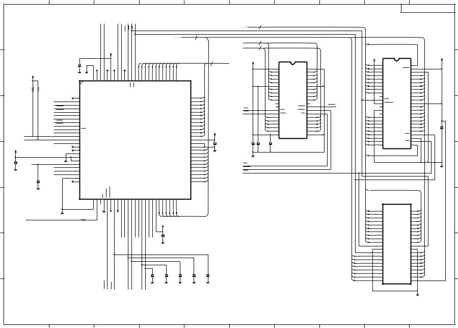
|
|
|
1 |
|
2 |
|
|
|
|
|
|
|
|
3 |
|
|
|
|
|
|
|
|
|
|
|
|
4 |
|
|
|
|
|
|
|
5 |
|
|
6 |
|
|
7 |
|
|
8 |
|
9 |
|
|
10 |
|
|
|
|
|
|
|
|
|
<01-F7> |
<01-F1> |
|
|
|
<04-B7> |
<04-B7> |
|
<02-F6> |
<02-F6> |
<02-F6> |
|
|
|
|
|
|
|
|
|
|
|
|
|
|
|
|
|
|
|
|
|
|
|
|
|
|
|
CONTROL PCB ASS'Y 03 |
||
|
|
|
|
|
|
|
|
|
|
|
|
|
|
|
|
|
|
|
|
|
|
|
|
|
|
|
|
|
|
|
|
|
|
|
|
|
|
|
|
|
|
|
|||||||
|
|
|
|
|
|
|
|
|
LFREF1 |
ON-VH |
|
|
|
PES |
HPS |
|
HWR |
WR |
RD |
|
|
|
|
|
|
|
|
|
|
|
|
|
|
|
|
|
<03-B6> |
A20~1 |
21 |
|
|
|
|
|
|
|
|
|
A |
|
|
|
|
|
|
|
|
|
|
|
|
|
|
|
|
|
|
|
|
|
|
|
|
|
|
|
|
|
|
<02-A6> |
|
|
|
|
|
|
|
|
|
|
|
|
|||||||
|
|
|
|
|
|
|
|
|
|
|
|
|
|
|
|
|
|
|
|
|
|
|
|
|
|
|
|
|
|
|
|
|
|
|
|
|
|
|
|
|
|
|
|
|
|
|
|
|
|
|
|
|
|
|
|
|
|
|
|
|
|
|
|
|
|
|
|
|
|
|
|
|
|
|
|
|
<02-A6> |
D15~0 |
16 |
|
|
|
|
|
|
|
|
|
|
|
|
|
|
|
|
||||
|
|
|
|
|
|
|
|
|
|
|
|
|
|
|
|
|
|
|
|
|
|
|
|
|
|
|
|
|
|
|
|
|
|
|
|
|
|
|
|
|
|
|
|
|
|
||||
|
|
|
|
|
|
|
|
|
|
|
|
|
|
|
|
|
|
|
|
|
|
|
|
|
|
|
|
|
|
|
|
|
|
|
|
|
<02-B1> |
MD15~0 |
16 |
|
|
|
|
17 |
|
|
|
|
|
|
|
|
|
|
|
|
|
|
|
|
|
|
|
|
|
|
|
|
|
|
|
|
|
|
|
|
|
|
|
|
|
|
|
|
|
|
|
|
|
|
|
|
|
|
|
|
|
||
|
|
|
|
|
|
|
|
|
|
|
|
|
|
|
|
|
|
|
|
|
|
|
|
|
|
|
|
|
|
|
|
|
|
|
|
|
<02-C1> |
MA9~0 |
10 |
|
|
|
|
|
CONTROL/CG ROM |
|
|
||
|
|
|
|
|
|
|
|
|
|
|
|
|
|
|
|
|
|
|
|
|
|
|
|
|
|
|
|
|
|
|
|
|
|
|
|
|
|
|
|
|
|
|
|
|
|
||||
|
|
|
|
|
|
|
|
|
|
|
Vcc1 |
|
|
|
|
|
|
|
|
|
|
|
|
|
|
|
|
|
|
|
|
|
|
|
|
|
|
|
DRAM |
|
|
|
|
|
|||||
|
|
|
|
|
|
|
|
|
|
|
|
|
|
|
|
|
|
|
|
|
|
|
|
|
|
|
|
|
|
|
|
|
|
|
|
|
|
|
|
|
|
|
|
|
|
||||
|
|
|
|
|
|
|
|
|
|
|
|
|
|
|
|
|
|
|
|
|
|
|
|
|
|
|
|
|
|
|
|
|
|
|
|
|
|
|
|
|
|
|
|
|
|
IC5 |
|
Vcc1 |
|
|
|
|
|
|
|
|
|
|
|
|
|
|
|
|
|
|
|
|
|
|
|
|
|
|
|
|
|
|
|
|
|
|
|
|
|
|
|
|
|
|
IC4 |
|
|
|
Vcc1 |
|
|
||
|
|
|
|
|
|
|
|
|
|
|
|
|
|
|
|
|
|
|
|
|
|
|
|
|
|
|
|
|
|
|
|
|
|
|
|
|
|
|
|
|
|
|
|
|
|
|
|||
|
|
|
|
|
|
|
|
|
|
|
|
|
|
|
|
|
|
|
|
|
|
|
|
|
|
|
|
|
|
|
|
|
|
|
24 |
A23~0 |
<02-A6> |
Vcc1 |
|
|
|
|
|
|
|
|
|
|
|
|
|
|
|
|
C25 |
|
|
|
|
|
|
|
|
|
|
|
|
|
|
|
|
|
|
|
|
|
|
|
|
|
|
|
|
|
|
|
|
|
|
16 |
1 |
|
48 |
|
|
||||
|
|
|
|
|
0.01μ, |
|
|
|
|
|
|
|
|
|
|
|
|
|
|
0 |
1 2 3 4 5 6 |
7 |
8 |
9 |
10 |
11 |
|
|
|
|
<03-A6> |
|
|
|
|
|
|
A15 |
|
|
|||||||||
|
|
|
|
|
|
|
|
|
|
|
|
|
|
|
|
|
|
|
|
|
|
|
|
|
|
1 |
40 |
|
|
15 |
2 |
A16 |
|
|
|||||||||||||||
|
|
|
|
|
|
|
CP13 |
CP14 CP15 |
CP19 |
|
|
|
|
|
|
|
|
|
|
|
|
|
|
|
|
|
|
|
|
|
|
|
|
|
47 |
|
|
||||||||||||
|
|
|
|
|
50V |
|
|
|
|
|
|
|
|
|
|
|
|
|
|
|
|
|
|
|
|
|
0 |
VCC1 |
VSS3 |
15 |
|
14 |
3 |
A14 |
BYTE |
|
B |
||||||||||||
|
|
|
|
|
|
|
|
|
|
|
|
|
|
|
|
|
|
|
|
|
|
|
|
|
|
|
|
|
|
|
|
|
|
|
|
|
|
|
2 |
39 |
|
A13 |
46 |
|
|||||
|
|
|
Vcc1 |
|
|
|
|
|
|
|
|
|
|
|
|
|
|
|
|
|
|
|
|
|
|
|
|
|
|
|
|
|
|
|
|
|
|
|
1 |
I/O0 |
I/O15 |
14 |
|
13 |
4 |
VSS2 |
15 |
||
|
|
|
|
|
|
|
|
|
|
|
|
|
|
|
|
|
|
|
|
|
|
|
|
|
|
|
|
|
|
|
|
|
|
|
|
|
|
3 |
38 |
|
A12 |
45 |
|
||||||
|
|
|
|
|
|
|
100 |
99 |
98 |
97 |
96 |
95 |
94 |
93 |
92 |
91 |
90 |
89 |
88 |
87 |
86 |
85 |
84 |
83 |
82 |
81 |
80 |
79 |
78 |
77 |
76 |
|
|
|
|
|
|
|
2 |
I/O1 |
I/O14 |
13 |
|
12 |
|
DQ15 |
7 |
|
|
|
|
|
|
|
|
|
|
|
|
|
|
|
|
4 |
37 |
|
5 |
A11 |
44 |
|
|||||||||||||||||||||||||||||
|
|
|
|
|
|
|
|
|
|
|
|
|
|
|
|
|
|
|
|
|
|
|
|
|
|
|
|
|
|
|
|
|
|
|
|
|
|
|
3 |
I/O2 |
I/O13 |
12 |
|
11 |
6 |
DQ7 |
14 |
|
|
|
|
|
|
|
|
|
|
|
|
|
|
|
|
|
|
|
|
|
|
|
|
|
|
|
|
|
|
|
|
|
|
|
|
|
|
|
|
|
5 |
36 |
|
A10 |
43 |
|
|||||
|
|
|
|
|
|
|
|
|
CS3/P63/CAS |
P62/CS2 |
P61/CS1 |
VCC4 |
P60/CS0 |
P55/R/W |
P54/BUSAK |
BUSROP53/ |
P52/HWR |
WR |
RD |
A0 |
A1 |
A2 |
A3 |
A4 |
A5 |
A6 |
A7 |
A8 |
A9 |
A10 |
A11 |
|
|
|
|
|
|
|
|
I/O3 |
I/O12 |
|
|
|
|
DQ14 |
|
|
|
|
|
|
1/16W |
1/16W |
CP16 |
|
P65/_REFOUT |
A12 |
|
|
|
|
|
|
7 |
10 |
31 |
8 |
|
|
11 |
A19 |
38 |
4 |
|
||||||||||||||||||||||||
|
|
|
|
|
GND4 |
RAS P64/ |
|
|
|
|
|
|
|
|
|
|
|
|
|
|
|
|
|
|
|
|
|
|
|
|
|
|
|
|
|
|
|
I/O5 |
I/O10 |
|
|
10 |
7 |
DQ5 |
6 |
|
|||
|
|
|
R352 |
R351 |
|
|
|
|
|
|
|
|
|
|
|
|
|
|
|
|
|
|
|
|
|
|
|
|
|
|
|
|
|
|
|
|
|
|
|
6 |
35 |
|
|
A9 |
42 |
|
|||
|
|
|
10K, |
10K, |
|
|
|
|
|
|
|
|
|
|
|
|
|
|
|
|
|
|
|
|
|
|
|
|
|
|
|
|
|
|
|
|
|
|
4 |
7 |
34 |
11 |
|
9 |
8 |
A8 |
41 |
13 |
|
|
|
|
|
|
|
|
|
|
|
|
|
|
|
|
|
|
|
|
|
|
|
|
|
|
|
|
|
|
|
|
|
|
|
|
|
|
|
|
5 |
8 |
33 |
10 |
|
20 |
9 |
|
40 |
5 |
|
|
|
|
|
|
|
1 |
|
|
|
|
|
|
|
|
|
|
|
|
|
|
|
|
|
|
|
|
|
|
|
|
|
|
75 |
12 |
|
|
|
|
6 |
9 |
32 |
9 |
|
|
10 |
NC1 |
39 |
12 |
|
|
|
|
|
|
|
|
|
|
|
|
|
|
|
|
|
|
|
|
|
|
|
|
|
|
|
|
|
|
|
|
|
|
|
|
|
|
I/O6 |
I/O9 |
|
|
|
|
DQ12 |
|
|
||||
|
|
|
|
<05-B1> |
ACRM |
2 |
P70/PG00 |
|
|
|
|
|
|
|
|
|
|
|
|
|
|
|
|
|
|
|
|
|
|
|
|
A13 |
74 |
13 |
|
|
|
|
|
I/O7 |
I/O8 |
|
|
|
12 |
WE |
DQ4 |
|
|
|
|
|
|
BCRM |
3 |
|
|
|
|
|
|
|
|
|
|
|
|
|
|
|
|
|
|
|
|
|
|
|
|
73 |
14 |
|
|
|
|
|
11 |
30 |
|
|
|
RESET |
37 |
|
|
||||
|
|
|
|
<05-B7> |
P71/PG01 |
|
|
|
|
|
|
|
|
|
|
|
|
|
|
|
|
|
|
|
|
|
|
|
|
A14 |
|
|
|
|
|
NC1 |
NC4 |
|
LCAS |
|
13 |
VCC |
11 |
|
|||||
|
|
|
|
ACRM |
4 |
|
|
|
|
|
|
|
|
|
|
|
|
|
|
|
|
|
|
|
|
|
|
|
|
72 |
15 |
|
|
|
|
|
12 |
29 |
|
<02-E1> |
NC2 |
36 |
|
||||||
|
|
|
|
<05-B1> |
P72/PG02 |
|
|
|
|
|
|
|
|
|
|
|
|
|
|
|
|
|
|
|
|
|
|
|
|
A15 |
|
|
|
UW |
|
NC2 |
LCAS |
|
|
14 |
DQ11 |
3 |
|
||||||
|
|
|
|
BCRM |
5 |
|
|
|
|
|
|
|
|
|
|
|
|
|
|
|
|
|
|
|
|
|
|
|
|
71 |
16 |
|
|
<02-D1> |
|
13 |
28 |
|
|
|
NC3 |
35 |
|
||||||
|
|
|
|
<05-B7> |
P73/PG03 |
|
|
|
|
|
|
|
|
|
|
|
|
|
|
|
|
|
|
|
|
|
|
|
|
P20/A16 |
|
|
RAS |
|
WE |
UCAS |
|
|
|
15 |
DQ3 |
10 |
|
||||||
|
|
|
|
ALFM |
6 |
|
|
|
|
|
|
|
|
|
|
|
|
|
|
|
|
|
|
|
|
|
|
|
|
70 |
17 |
|
|
<02-D1> |
|
14 |
27 |
|
|
|
RY/_BY |
34 |
|
||||||
|
|
|
|
<05-F1> |
P74/PG10 |
|
|
|
|
|
|
|
|
|
|
|
|
|
|
|
|
|
|
|
|
|
|
|
|
P21/A17 |
|
|
|
9 |
RAS |
OE |
8 |
|
19 |
16 |
DQ10 |
2 |
C |
||||||
|
|
|
|
BLFM |
7 |
|
|
|
|
|
|
|
|
|
|
|
|
|
|
|
|
|
|
|
|
|
|
|
|
69 |
18 |
|
|
|
|
15 |
26 |
|
A18 |
33 |
|||||||||
|
|
|
|
<05-F1> |
P75/PG11 |
|
|
|
|
|
|
|
|
|
|
|
|
|
|
|
|
|
|
|
|
|
|
|
|
P22/A18 |
|
|
|
|
0 |
NC3 |
A8 |
7 |
|
18 |
17 |
DQ2 |
9 |
||||||
|
|
|
|
ALFM |
8 |
|
|
|
|
|
|
|
|
|
|
|
|
|
|
|
|
|
|
|
|
|
|
|
|
68 |
19 |
|
|
|
|
16 |
25 |
|
A17 |
32 |
|
||||||||
|
|
|
|
<05-F1> |
P76/PG12 |
|
|
|
|
|
|
|
|
|
|
|
|
|
|
|
|
|
|
|
|
|
|
|
|
P23/A19 |
|
|
|
|
1 |
A0 |
A7 |
6 |
|
8 |
18 |
DQ9 |
1 |
|
|||||
|
|
|
|
BLFM |
9 |
|
|
|
|
|
|
|
|
|
|
|
|
|
|
|
|
|
|
|
|
|
|
|
|
67 |
20 |
|
|
|
|
17 |
24 |
|
A7 |
31 |
|
||||||||
|
|
|
|
<05-F1> |
P77/PG13 |
|
|
|
|
|
|
|
|
|
|
|
|
|
|
|
|
|
|
|
|
|
|
|
|
P24/A20 |
|
|
|
|
2 |
A1 |
A6 |
5 |
|
7 |
19 |
DQ1 |
8 |
C404 |
|||||
|
|
|
|
FPWRON |
10 |
|
|
|
|
|
|
|
|
|
|
|
|
|
|
|
|
|
|
|
|
|
|
|
|
66 |
21 |
|
|
|
|
18 |
23 |
|
A6 |
30 |
|||||||||
|
|
|
|
<02-G1> |
NMI |
|
|
|
|
|
|
|
|
|
|
|
|
|
|
|
|
|
|
|
|
|
|
|
|
P25/A21 |
|
|
|
|
3 |
A2 |
A5 |
4 |
|
6 |
20 |
DQ8 |
0 |
0.01μ,50V |
|||||
|
|
|
|
TOPC |
11 |
|
|
|
|
|
|
|
|
|
|
|
|
|
|
|
|
|
|
|
|
|
|
|
|
65 |
22 |
Vcc1 |
|
|
19 |
22 |
|
A5 |
29 |
||||||||||
|
|
|
|
<02-C7> |
P80/TXD0 |
|
|
|
|
|
|
|
|
|
|
|
|
|
|
|
|
|
|
|
|
|
|
|
|
P26/A22 |
|
|
|
A3 |
A4 |
|
|
5 |
21 |
DQ0 |
|
|
|||||||
|
|
|
IDO |
|
12 |
|
|
|
|
|
|
|
|
|
|
|
|
|
|
|
|
|
|
|
|
|
|
|
|
64 |
23 |
|
|
|
|
|
20 |
21 |
|
|
A4 |
28 |
|
|
|||||
|
<02-C7> |
|
|
P81/RXD0 |
|
|
|
|
|
|
|
|
|
|
|
|
|
|
|
|
|
|
|
|
|
|
|
|
P27/A23 |
|
|
|
|
|
VCC3 |
VSS1 |
|
|
4 |
22 |
OE |
|
|
||||||
|
ID1 |
|
|
13 |
|
|
|
|
|
|
|
|
|
|
CPU |
|
|
|
|
|
|
|
|
|
|
|
63 |
|
|
|
|
|
|
|
|
|
|
A3 |
27 |
|
|
||||||||
|
<02-C7> |
|
|
P82/_CTS0/SCLK0 |
|
|
|
|
|
|
|
|
|
|
|
|
|
|
|
|
|
|
VCC3 |
|
|
C26 |
|
|
|
|
|
|
|
3 |
23 |
VSS1 |
|
|
|||||||||||
|
|
|
E-DO |
14 |
|
|
|
|
|
|
|
|
IC6 |
|
|
|
|
|
|
|
|
|
|
|
62 |
|
|
|
C401 |
C402 |
C403 |
|
|
|
A2 |
26 |
|
|
|||||||||||
|
|
|
|
<05-D10> |
P83/TXD1 |
|
|
|
|
|
|
|
|
|
|
|
|
|
|
|
|
|
|
|
|
|
|
GND3 |
|
|
0.01μ, |
|
|
|
|
2 |
24 |
CE |
|
|
|||||||||
|
|
|
|
|
15 |
|
|
|
|
|
|
|
|
|
|
|
|
|
|
|
|
|
|
|
|
|
|
61 |
|
|
|
0.01μ, |
0.01μ, |
0.01μ, |
|
|
|
A1 |
25 |
|
|
||||||||
|
Vcc1 |
|
|
|
CP10 |
P84/RXD1 |
|
|
|
|
|
|
|
|
|
|
|
|
|
|
|
|
|
|
|
|
|
|
|
|
GND2 |
|
|
50V |
|
|
|
|
|
|
A0 |
|
|
||||||
|
|
|
|
16 |
|
|
|
|
|
|
|
|
|
|
|
|
|
|
|
|
|
|
|
|
|
|
|
|
60 |
|
15 |
|
50V |
50V |
50V |
|
|
|
|
|
|
|
|
|
|||||
|
|
|
|
|
CP12 |
P85/SCLK1 |
|
|
|
|
|
|
|
|
|
|
|
|
|
|
|
|
|
|
|
|
|
|
|
|
P17/D15 |
|
|
|
|
|
|
|
|
|
|
|
|
||||||
|
|
|
|
|
17 |
|
|
|
|
|
|
|
|
|
|
|
|
|
|
|
|
|
|
|
|
|
|
|
|
59 |
|
14 |
|
|
|
|
|
|
|
|
|
|
|
|
|
|
|||
|
|
|
|
|
|
AGND |
|
|
|
|
|
|
|
|
|
|
|
|
|
|
|
|
|
|
|
|
|
|
|
|
P16/D14 |
|
|
|
|
|
|
|
|
|
1 |
|
|
|
|
|
|||
17 |
|
|
|
|
|
18 |
|
|
|
|
|
|
|
|
|
|
|
|
|
|
|
|
|
|
|
|
|
|
|
|
58 |
|
13 |
|
|
|
|
|
|
|
|
|
|
|
|
|
|||
|
|
|
|
|
VREF |
|
|
|
|
|
|
|
|
|
|
|
|
|
|
|
|
|
|
|
|
|
|
|
|
P15/D13 |
|
|
|
|
|
|
|
|
|
|
|
|
|
|
|
||||
C27 |
|
|
|
|
19 |
|
|
|
|
|
|
|
|
|
|
|
|
|
|
|
|
|
|
|
|
|
|
|
|
57 |
|
12 |
|
|
|
|
|
|
|
|
|
|
|
|
|
|
|||
|
DCLVL |
|
VCC1 |
|
|
|
|
|
|
|
|
|
|
|
|
|
|
|
|
|
|
|
|
|
|
|
|
P14/D12 |
|
|
|
|
|
|
|
|
|
|
|
|
|
|
D |
||||||
0.01μ, |
|
|
20 |
|
|
|
|
|
|
|
|
|
|
|
|
|
|
|
|
|
|
|
|
|
|
|
|
56 |
|
11 |
|
|
|
|
|
|
|
|
|
|
|
|
|
||||||
|
|
P90/AN0 |
|
|
|
|
|
|
|
|
|
|
|
|
|
|
|
|
|
|
|
|
|
|
|
|
P13/D11 |
|
|
|
OE |
|
|
|
|
|
|
|
|
|
|
||||||||
<01-G7> |
|
|
|
|
|
|
|
|
|
|
|
|
|
|
|
|
|
|
|
|
|
|
|
|
|
|
|
10 |
|
<02-E1> |
|
|
|
|
|
|
|
|
|
|
|||||||||
|
50V |
|
|
<02-F6> |
HDIS |
21 |
P91/AN1 |
|
|
|
|
|
|
|
|
|
|
|
|
|
|
|
|
|
|
|
|
|
|
|
|
P12/D10 |
55 |
|
|
UCAS |
|
|
|
|
|
|
|
|
|
|
|
||
|
|
|
|
HRANK |
22 |
|
|
|
|
|
|
|
|
|
|
|
|
|
|
|
|
|
|
|
|
|
|
|
|
54 |
|
9 |
|
<02-E1> |
|
|
|
|
|
|
|
|
|
|
|
||||
|
|
|
|
<02-C7> |
P92/AN2 |
|
|
|
|
|
|
|
|
|
|
|
|
|
|
|
|
|
|
|
|
|
|
|
|
P11/D9 |
|
|
CE1 |
|
|
|
|
|
|
|
|
|
|
|
|||||
|
|
|
|
THLVL |
23 |
|
|
|
|
|
|
|
|
|
|
|
|
|
|
|
|
|
|
|
|
|
|
|
|
53 |
|
8 |
|
<02-A4> |
|
|
|
|
|
|
|
|
|
|
|
||||
|
|
|
|
<04-G6> |
P93/AN3 |
|
|
|
|
|
|
|
|
|
|
|
|
|
|
|
|
|
|
|
|
|
|
|
|
P10/D8 |
|
|
|
|
|
|
|
|
|
|
|
|
|
|
|||||
|
|
|
|
|
24 |
|
|
|
|
|
|
|
|
|
|
|
|
|
|
|
|
|
|
|
|
|
|
|
|
52 |
|
7 |
|
|
|
|
|
|
|
|
|
|
|
|
|
|
|||
|
|
|
C24 |
|
|
AM8/_16 |
|
|
|
|
|
|
|
|
|
|
|
|
|
|
|
|
|
|
|
|
|
|
|
|
D7 |
|
|
|
|
|
|
|
|
|
|
|
|
|
|
|
|||
|
|
|
|
|
25 |
|
|
|
|
|
|
|
|
|
|
|
|
|
|
|
|
|
|
|
|
|
|
|
|
51 |
|
6 |
|
|
|
|
|
|
|
|
|
|
|
|
|
|
|||
|
|
|
|
CP11 |
CLK |
|
|
|
|
|
|
|
|
|
|
|
|
|
|
|
|
|
|
|
|
|
|
|
|
D6 |
|
|
|
|
|
|
|
|
|
|
|
|
|
|
|
||||
|
|
|
0.01μ, |
|
|
|
|
|
|
|
|
|
|
|
|
|
|
|
|
|
|
|
|
|
|
|
|
|
|
|
|
|
|
|
|
|
|
|
|
|
|
|
|
||||||
|
|
|
|
|
X1 |
X2 |
EA |
RESET |
WDTOUT |
WAITPA0/ |
PA1/TI0 |
PA2/TO1 |
PA3/TO3 |
PB0/INT4/TI4 |
PB1/INT5/TI5 |
PB2/TO4 |
PB3/TO5 |
PB4/INT6/TI6 |
PB5/INT7/TI7 |
PB6/TO6 |
PB7/INT0 |
VCC2 |
D0 |
D1 |
D2 |
D3 |
D4 |
D5 |
|
|
|
|
|
|
|
|
|
|
|
|
|
|
|
|
|
||||
|
|
|
50V |
|
|
|
GND1 |
|
|
|
|
|
|
|
|
|
|
|
|
|
|
|
|
|
|
||||||||||||||||||||||||
|
|
|
|
|
|
|
26 |
27 |
28 |
29 |
30 |
31 |
32 |
33 |
34 |
35 |
36 |
37 |
38 |
39 |
40 |
41 |
42 |
43 |
44 |
45 |
46 |
47 |
48 |
49 |
50 |
|
|
|
|
|
|
|
|
|
|
|
|
|
|
ICS5 (Not mounted) |
|
|
|
|
|
|
|
|
|
|
|
|
|
|
|
|
|
|
|
|
|
|
|
|
|
|
|
|
|||||||||||||||||||||||||
|
|
|
|
|
|
|
|
|
|
|
|
|
|
|
|
|
|
|
|
|
|
|
|
|
|
|
|
|
|
|
|
|
|
|
|
|
|
|
|
|
|
|
|
19 |
1 |
|
42 |
20 |
E |
|
|
|
|
|
|
|
|
|
|
|
CP18 CP17 |
|
|
|
|
|
|
|
|
|
|
|
0 1 2 3 4 5 |
|
|
|
|
|
|
|
|
|
|
|
18 |
2 |
|
41 |
9 |
|
|||||||||
|
|
|
SXOUT |
|
|
|
|
|
|
|
|
|
|
|
|
|
|
|
|
|
|
|
|
|
|
|
|
|
|
|
|
|
|
|
|
|
|
|
|
|
|
|
|
8 |
3 |
|
40 |
10 |
|
|
<02-A6> |
|
|
|
|
|
|
|
|
|
|
|
|
|
|
|
|
|
|
|
|
|
|
|
|
|
|
|
|
|
|
|
|
|
|
|
|
|
|
|
|
7 |
4 |
|
39 |
11 |
|
||
|
|
|
|
|
R13 |
|
|
|
|
|
|
|
|
|
|
|
|
|
|
|
|
|
|
Vcc1 |
|
|
|
|
|
|
|
|
|
|
|
|
|
|
|
|
|
||||||||
|
|
|
|
|
|
|
|
|
|
|
|
|
|
|
|
|
|
|
|
|
|
|
|
|
|
|
|
|
|
|
|
|
|
|
|
|
|
|
|
6 |
5 |
|
38 |
12 |
|
||||
|
|
|
|
|
|
300,1/16W |
|
|
|
|
|
|
|
CRREF1 |
CRREF2 |
|
|
DIO-TE |
CLK-TE |
|
|
OE-E |
OE-T |
|
|
|
|
|
|
|
|
|
|
|
|
|
|
|
|
|
|
|
5 |
6 |
|
37 |
13 |
|
|
|
|
|
|
|
|
|
|
|
|
|
|
|
|
|
|
|
|
|
|
|
|
C34 |
|
|
|
|
|
|
|
|
|
|
|
|
|
|
4 |
7 |
|
36 |
14 |
|
|||||||
|
|
|
|
|
|
|
|
|
|
|
|
|
|
|
|
|
|
|
|
|
|
|
|
|
|
|
|
|
|
|
|
|
|
|
|
|
|
|
|
|
|
3 |
8 |
|
35 |
15 |
|
||
|
|
|
|
|
|
|
|
|
|
|
|
|
|
|
|
|
|
|
|
|
|
|
|
|
|
|
|
0.01μ, |
|
|
|
|
|
|
|
|
|
|
|
|
|
|
|
||||||
|
|
|
|
|
|
|
|
|
|
|
|
|
|
|
|
|
|
|
|
|
|
|
|
|
|
|
|
|
|
|
|
|
|
|
|
|
|
|
|
|
2 |
9 |
|
34 |
16 |
|
|||
|
|
|
|
|
|
|
|
|
|
|
|
|
|
|
|
|
|
|
|
|
|
|
|
|
|
|
|
50V |
|
|
|
|
|
|
|
|
|
|
|
|
|
|
|
|
|||||
|
|
|
|
|
|
|
|
|
|
|
|
|
|
|
-<05B1> |
-<05B7> |
|
|
-<05E7> |
D7>-<05 |
|
|
D7>-<05 |
C7>-<05 |
|
|
|
|
|
|
|
|
|
|
|
|
|
|
|
|
|
1 |
10 |
|
33 |
17 |
|
||
|
|
|
|
|
|
|
|
|
|
|
|
|
|
|
|
|
|
|
|
|
|
|
|
|
|
|
|
|
|
|
|
|
|
|
|
|
|
|
|
||||||||||
|
|
|
|
|
|
|
|
|
|
|
|
|
|
|
|
|
|
|
|
|
|
|
|
|
|
|
|
|
|
|
|
|
|
|
|
|
|
|
11 |
|
32 |
|
|
||||||
|
|
|
|
|
|
|
|
|
|
|
|
|
|
|
|
|
|
|
|
|
|
|
|
|
|
|
|
|
|
|
|
|
|
|
|
|
|
|
|
|
|
|
|
|
12 |
|
31 |
|
|
|
|
|
|
|
|
|
|
|
|
|
|
|
|
|
|
|
|
|
|
|
|
|
|
|
|
|
|
|
|
|
|
|
|
|
|
|
|
|
|
|
|
|
|
|
13 |
|
30 |
15 |
F |
|
|
|
|
|
|
|
|
|
|
|
|
|
|
|
|
|
|
|
|
|
|
|
|
|
|
|
|
|
|
|
|
|
|
|
|
|
|
|
|
|
|
|
|
0 |
14 |
|
29 |
7 |
|
|
|
|
|
|
|
|
|
|
|
|
|
|
|
|
|
|
|
|
|
|
|
|
|
|
|
|
|
|
|
|
|
|
|
|
|
|
|
|
|
|
|
|
|
8 |
15 |
|
28 |
14 |
|
|
|
|
|
|
|
|
|
|
|
|
|
|
|
|
|
|
|
|
|
|
|
|
|
|
|
|
|
|
|
|
|
|
|
|
|
|
|
|
|
|
|
|
|
1 |
16 |
|
27 |
6 |
|
|
|
|
|
|
|
|
|
|
|
|
|
|
|
|
|
|
|
|
|
|
|
|
|
|
|
|
|
|
|
|
|
|
|
|
|
|
|
|
|
|
|
|
|
9 |
17 |
|
26 |
13 |
|
|
|
|
|
|
|
|
|
|
|
|
|
|
|
|
|
|
|
|
|
|
|
|
|
|
|
|
|
|
|
|
|
|
|
|
|
|
|
|
|
|
|
|
|
2 |
18 |
|
25 |
5 |
|
|
|
|
|
|
|
|
|
|
|
|
|
|
|
|
|
|
|
|
|
|
|
|
|
|
C23 |
|
|
C32 |
|
C30 |
|
C33 |
C31 |
|
|
|
|
|
|
|
|
10 |
19 |
|
24 |
12 |
|
||
|
|
|
|
|
|
|
|
|
|
|
|
|
|
|
|
|
|
|
|
|
|
|
|
|
100p, |
|
100p, |
100p, |
|
100p, |
SPEC/ |
|
|
|
|
|
|
|
3 |
20 |
|
23 |
4 |
|
|||||
|
|
|
|
|
|
|
|
|
|
|
RESET |
|
|
|
|
|
|
|
|
|
|
|
|
|
50V |
|
|
50V |
|
50V |
|
50V |
NOPART |
|
|
|
|
|
|
|
11 |
21 |
|
22 |
|
|
|||
|
|
|
|
|
|
|
|
|
|
|
|
WAIT |
|
|
|
INT4 |
INT5 |
|
|
INT6 |
INT7 |
|
|
|
|
|
|
|
|
|
|
|
|
|
|
|
|
|
|
|
|
|
|
|
|
|
|
|
|
|
|
|
|
|
|
|
|
|
|
|
<01-B10> <02-F1> |
<02-A3> |
|
|
|
<02-A4> |
<02-A4> |
|
|
<02-A4> |
<02-A4> |
|
|
|
|
|
|
|
|
|
|
|
|
|
|
|
|
|
|
|
|
|
|
|
|
|
|
|
|
|
1 |
|
|
2 |
|
3 |
|
4 |
|
|
|
5 |
|
|
|
6 |
|
7 |
|
|
8 |
|
9 |
10 |
|
|
|
|
|
|
|
|
|
|
|
|
|
|
|
|
|
|
|
|
|
|
|
|
|
|
|
CONTROL PCB ASS'Y 04 |
|
|
|
|
|
|
|
|
|
|
|
|
|
|
|
|
|
|
|
|
|
|
|
|
|
|
|
A |
|
|
|
Vcc3 |
Vif |
|
|
|
|
|
|
|
|
|
|
|
|
|
|
|
|
|
|
|
|
|
|
|
|
|
|
|
|
|
|
|
R504 |
R505 |
|
|
|
|
|
|
|
|
|
|
|
|
|
|
|
|
|
|
|
R501 |
R502 |
R503 |
|
|
|
100,1/16W |
1K,1/16W |
|
|
|
|
|
|
STB |
<02-G4> |
|
|
|
|
Vcc3 |
Vcc1 |
CNPI |
|
|
|
|
|
|
|
|
|
|
|
|
|
|
|
|
|
|
|
|
|
|
|
|||||
|
|
|
|
|
|
|
|
|
|
|
|
|
|
|
|
|
|
|
|
|
|
|
||||
|
|
|
390, |
1K, |
1K, |
|
|
|
|
|
|
|
|
|
|
|
|
|
|
|
|
|
|
|
|
|
|
Parallel Interface |
1/8W |
1/16W |
1/16W |
|
|
|
|
C501 |
|
|
|
|
|
|
|
|
|
|
|
|
|
|
22 |
|
|
|
|
|
RA1 |
2 4 6 8 |
RA2 |
2 4 6 8 |
|
1000p,50V |
|
|
|
|
|
|
|
|
<02-G3> |
BZOUT |
R515 |
100,1/16W |
|
|
21 |
|
||
|
|
|
|
|
|
|
|
|
|
|
|
|
|
|
|
|
|
|
|
|
20 |
|
||||
|
|
|
|
|
|
|
|
|
|
|
|
|
|
|
|
|
|
|
PES |
R516 |
100,1/16W |
|
|
|
||
|
|
CNIF1 |
|
|
|
|
|
|
|
|
|
|
|
|
|
|
|
|
<02-A3> |
|
|
19 |
B |
|||
|
|
|
|
|
1 3 5 7 |
|
1 3 5 7 |
|
|
|
|
|
|
|
|
|
|
HPS |
R517 |
100,1/16W |
|
|
||||
|
|
|
|
|
|
|
|
|
|
|
|
|
|
|
|
|
<02-A3> |
|
|
18 |
||||||
|
|
|
|
|
|
|
|
|
|
|
|
|
|
|
|
|
|
|
PW-LED |
R518 |
300,1/16W |
|
|
|
||
|
STROBE |
1 |
|
|
|
|
|
|
|
|
|
|
|
|
|
|
|
|
<02-G3> |
|
|
17 |
|
|||
|
|
|
|
|
|
|
|
|
|
|
|
|
|
|
IFD0 |
|
ERR-LED |
R519 |
300,1/16W |
|
|
|
||||
|
DATA1 |
2 |
|
|
|
|
|
|
|
|
|
|
|
|
|
|
<02-G4> |
<02-G3> |
|
|
16 |
|
||||
|
|
|
|
|
|
|
|
|
|
|
|
|
|
|
IFD1 |
|
|
|
|
|
|
|||||
|
DATA2 |
3 |
|
|
|
|
|
|
|
|
|
|
|
|
|
|
<02-G4> |
|
|
|
|
Vcc1 |
|
|
|
|
|
|
|
|
|
|
|
|
|
|
|
|
|
|
|
IFD2 |
|
|
|
|
|
|
|
||||
|
DATA3 |
4 |
|
|
|
|
|
|
|
|
|
|
|
|
|
|
<02-G4> |
|
|
|
|
|
|
|
||
|
|
|
|
|
|
|
|
|
|
|
|
|
|
|
|
|
|
|
|
|
|
|
||||
|
|
|
|
|
|
|
|
|
|
|
|
|
|
|
IFD3 |
|
|
|
|
|
|
|
|
|||
|
DATA4 |
5 |
|
|
|
|
|
|
|
|
|
|
|
|
|
|
<02-G4> |
|
|
|
|
|
|
|
|
|
|
|
|
|
|
|
|
|
|
|
|
|
|
|
|
IFD4 |
|
|
|
|
R511 |
|
|
|
|||
|
DATA5 |
6 |
|
|
|
|
|
|
|
|
|
|
|
|
|
|
<02-G4> |
|
|
R512 |
|
|
|
|
||
|
|
|
|
|
|
|
|
|
|
|
|
|
|
|
IFD5 |
|
|
|
10K,1/16W |
|
|
|
||||
|
DATA6 |
7 |
|
|
|
|
|
|
|
|
|
|
|
|
|
|
<02-G4> |
|
|
100,1/16W |
|
|
|
|
||
|
|
|
|
|
|
|
|
|
|
|
|
|
|
|
IFD6 |
|
PWRON |
|
|
|
|
|
||||
|
DATA7 |
8 |
|
|
|
|
|
|
|
|
|
|
|
|
|
|
<02-G4> |
<02-G2> |
|
|
|
|
15 |
|
||
|
|
|
|
|
|
|
|
|
|
|
|
|
|
|
IFD7 |
|
|
|
|
|
|
|||||
|
DATA8 |
9 |
|
|
|
|
|
|
|
|
|
|
|
|
|
|
<02-G4> |
|
|
|
C521 |
|
|
|
|
|
|
|
|
|
|
|
|
|
|
|
|
|
|
|
|
|
|
|
|
|
|
|
|
||||
|
ACK |
10 |
|
|
|
|
|
|
C502 |
C503 |
C504 |
C505 |
C506 |
C507 |
|
C508 |
C509 |
|
|
|
0.01μ,50V |
Vcc1 |
|
|
|
|
|
BUSY |
11 |
|
|
|
|
|
|
|
|
|
|
|
|
|
To PANEL BOARD |
|
|||||||||
|
|
|
|
|
|
|
1000p, |
1000p, |
1000p, |
1000p, |
1000p, |
1000p, |
1000p, |
1000p, |
|
|
|
|
|
|
|
|
||||
|
PE |
12 |
|
|
|
|
|
|
|
|
|
|
|
|
|
C |
||||||||||
|
|
|
|
|
|
|
50V |
50V |
50V |
50V |
50V |
50V |
|
50V |
50V |
|
|
|
|
|
R520 |
|
|
|||
|
SLCT |
13 |
|
|
|
|
|
|
|
|
|
|
R513 |
|
|
|
||||||||||
|
|
|
RA3 |
2 4 6 8 |
RA4 |
2 4 6 8 |
|
|
|
|
|
|
|
|
|
|
|
|
|
|
|
|||||
|
AUTXT |
14 |
|
|
|
|
|
|
|
|
|
|
|
|
|
|
100,1/16W |
|
10K,1/16W |
|
|
|
||||
|
|
|
|
|
|
|
|
|
|
|
|
|
|
|
|
|
|
|
|
|
|
|
||||
|
|
|
|
|
|
|
|
|
|
|
|
|
|
|
|
|
|
CC-SW |
|
|
|
|
|
|||
|
NC |
15 |
|
|
|
|
|
|
|
|
|
|
|
|
|
|
|
|
<02-G3> |
|
|
|
|
14 |
|
|
|
|
|
|
1 3 5 7 |
|
1 3 5 7 |
|
|
|
|
|
|
|
|
|
|
|
|
|
|
|
|
||||
|
S-GND |
16 |
|
|
|
|
|
|
|
|
|
|
|
|
|
|
|
|
|
C522 |
|
|
|
|
||
|
|
|
|
|
|
|
|
|
|
|
|
|
|
|
|
|
|
|
|
|
|
|
|
|||
|
F-GND |
17 |
|
|
|
|
|
|
|
|
|
|
|
|
|
|
|
|
|
|
0.01μ,50V |
Vcc1 |
|
|
|
|
|
+5V |
18 |
|
|
|
|
|
|
|
|
|
|
|
|
|
|
|
|
|
|
|
|
|
|
|
|
|
|
|
|
|
|
|
|
|
|
|
|
|
|
|
|
|
|
|
|
|
|
|
|
|
||
|
S-GND |
19 |
|
|
|
|
|
|
R509 |
|
|
|
|
|
|
|
|
|
|
|
|
|
R521 |
|
|
|
|
S-GND |
20 |
|
|
|
|
|
|
1K,1/16W |
|
|
|
|
|
|
|
|
|
|
|
R514 |
|
|
|
|
|
|
|
|
|
|
|
|
|
|
|
|
|
|
|
AUTXT |
<02-G4> |
|
|
|
10K,1/16W |
|
|
|
||||
|
S-GND |
21 |
|
|
|
|
|
|
|
|
|
|
|
|
|
|
|
|
100,1/16W |
|
|
|
|
|||
|
|
|
|
|
|
|
|
|
|
|
|
|
|
|
|
|
RCV-SW |
|
|
|
|
|
||||
|
S-GND |
22 |
|
|
|
|
|
|
|
|
|
|
|
|
|
|
|
|
<02-G3> |
|
|
|
|
13 |
|
|
|
|
|
|
|
|
|
|
|
|
|
|
|
|
|
ACK |
|
|
|
|
|
|
|
||||
18 |
S-GND |
23 |
|
|
|
|
|
|
|
|
|
|
|
|
|
|
<02-G4> |
|
|
|
C523 |
|
|
12 |
|
|
|
|
|
|
|
|
|
|
|
|
|
|
|
|
|
|
|
|
|
|
|
||||||
S-GND |
24 |
|
|
|
|
|
|
|
|
|
|
|
|
|
|
BUSY |
|
|
|
0.01μ,50V |
|
|
11 |
|
||
|
S-GND |
25 |
|
|
|
|
|
|
|
|
|
|
|
|
|
|
<02-G4> |
|
|
|
|
|
|
|
D |
|
|
|
|
|
|
|
|
|
|
|
|
|
|
|
|
|
|
|
|
|
|
|
|
||||
|
S-GND |
26 |
Vcc3 |
|
|
|
|
|
|
|
|
|
|
|
|
PE |
|
|
|
|
|
|
|
|
||
|
S-GND |
27 |
|
|
|
|
|
|
|
|
|
|
|
|
|
|
<02-G4> |
|
|
|
|
|
|
|
|
|
|
|
|
|
|
|
|
|
|
|
|
|
|
|
|
|
|
|
|
|
|
|
|
|
|||
|
S-GND |
28 |
|
R510 |
|
|
|
|
|
|
|
|
|
|
|
SLCT |
|
|
|
|
|
|
|
|
|
|
|
S-GND |
29 |
|
5.6K,1/16W |
|
|
|
|
|
|
|
|
|
|
|
<02-G4> |
|
|
|
|
|
|
|
|
||
|
|
|
|
R506 |
R507 |
|
|
|
|
|
|
|
|
|
|
|
|
|
|
|
|
|||||
|
S-GND |
30 |
|
|
|
|
|
|
|
|
|
|
|
|
|
|
|
|
|
|
|
|
10 |
|
||
|
|
|
|
|
|
100,1/16W |
1K,1/16W |
|
|
|
|
|
|
|
INIT |
|
|
|
|
|
|
|
|
|||
|
INPRM |
31 |
|
|
|
|
|
|
|
|
|
|
|
|
<02-G4> |
|
|
|
|
|
|
|
|
|||
|
|
|
|
|
|
|
|
|
|
|
|
|
|
|
|
|
|
|
|
|
|
|
||||
|
|
|
|
|
|
|
|
|
|
|
|
|
|
|
|
|
FRXD |
|
|
|
|
|
|
|||
|
FAILT |
32 |
|
|
|
|
|
|
|
|
|
|
|
|
|
|
|
|
<02-G1> |
|
|
|
|
9 |
|
|
|
|
|
|
|
|
|
|
|
|
|
|
|
|
|
FAULT |
|
|
|
|
|
|
|
||||
|
S-GND |
33 |
|
|
|
|
|
|
|
|
|
|
|
|
|
|
<02-G4> |
|
|
|
|
|
|
|
|
|
|
|
|
|
|
|
|
|
|
|
|
|
|
|
|
|
|
|
|
|
|
|
|
|
|||
|
NC |
34 |
|
|
|
|
|
|
|
|
|
|
|
|
|
|
|
|
|
|
|
|
|
|
8 |
|
|
+5V |
35 |
|
|
|
|
|
|
|
|
|
|
|
|
|
|
|
|
|
RXD |
|
|
|
|
|
|
|
SELIN |
36 |
|
|
|
|
|
|
|
|
|
|
|
|
|
|
|
|
<02-G1> |
|
|
|
|
7 |
|
|
|
|
|
|
|
|
|
C516 |
C511 |
C512 |
C513 |
C514 |
|
C515 |
|
|
|
|
|
|
|
|
|||||
|
FG1 |
|
|
|
|
|
|
|
|
|
|
|
|
|
|
|
|
To IrDA UNIT |
|
|||||||
|
|
|
|
|
|
|
|
0.01μ, |
1000p, |
1000p, |
1000p, |
1000p, |
1000p, |
|
|
|
|
|
|
|
|
|
||||
|
FG2 |
|
|
|
|
|
|
|
|
|
|
|
R532 |
|
|
|
6 |
|
||||||||
|
|
|
|
|
|
|
|
50V |
50V |
50V |
50V |
50V |
|
50V |
|
|
|
|
|
|
|
|
E |
|||
|
|
|
|
|
|
|
|
|
|
|
|
|
|
|
|
|
|
|
||||||||
|
|
|
|
|
|
|
|
|
|
|
|
|
|
|
68,1/16W |
|
|
|
|
|||||||
|
|
|
|
|
|
|
|
|
|
|
|
|
|
|
|
|
|
|
<02-G3> |
TXD |
|
|
|
5 |
||
|
|
|
|
|
|
|
|
|
|
|
|
|
|
|
|
|
|
|
|
|
|
|
|
|||
|
|
|
|
|
|
|
|
|
|
|
|
|
|
|
|
|
|
|
|
|
|
|
|
|
||
|
|
|
|
|
|
|
|
|
R508 |
|
|
|
|
|
|
|
|
|
|
|
|
|
|
|
4 |
|
|
|
|
|
|
|
|
|
|
|
|
|
|
|
|
|
|
|
|
|
|
|
|
|
|
|
|
|
|
|
|
|
|
|
|
|
1K,1/16W |
|
|
|
|
|
|
|
SELIN |
<02-G3> |
<02-G2> |
MODE |
|
|
|
|
Vcc1 |
|
|
|
|
|
|
|
|
|
|
|
|
|
|
|
|
|
|
|
|
|
|
3 |
|
||||
|
|
|
|
|
|
|
|
|
|
|
|
|
|
|
|
|
|
|
|
|
|
|
|
|||
|
|
|
|
|
|
|
|
|
|
|
|
|
|
|
|
|
|
|
|
|
|
|
|
|
2 |
|
|
|
|
|
|
|
|
|
|
|
|
|
|
|
|
|
|
|
|
|
|
|
|
|
|
1 |
|
|
|
|
|
|
|
|
|
|
|
|
|
|
|
|
|
|
|
|
|
|
|
|
|
|
|
F |
|
|
|
|
|
|
|
|
|
|
|
|
|
|
|
|
Vcc1 |
|
|
|
|
|
|
|
|
|
|
|
|
|
|
|
|
|
|
|
|
|
|
|
|
|
|
TH1 |
|
|
|
|
|
|
|
|
|
|
|
|
|
|
|
|
|
|
|
|
|
|
|
|
|
|
|
THLVL |
|
|
|
|
|
|
|
|
|
|
|
|
|
|
|
|
|
|
|
|
|
|
|
|
|
R531 |
|
<03-D2> |
|
|
|
|
|
|
|
|
|
|
|
|
|
|
|
|
|
|
|
|
|
|
|
|
|
|
|
|
|
|
|
|
|
|
|
|
|
|
|
|
|
|
|
|
|
|
|
|
|
|
|
47K,1/16W |
|
|
|
|
|
|
|
|
|
|
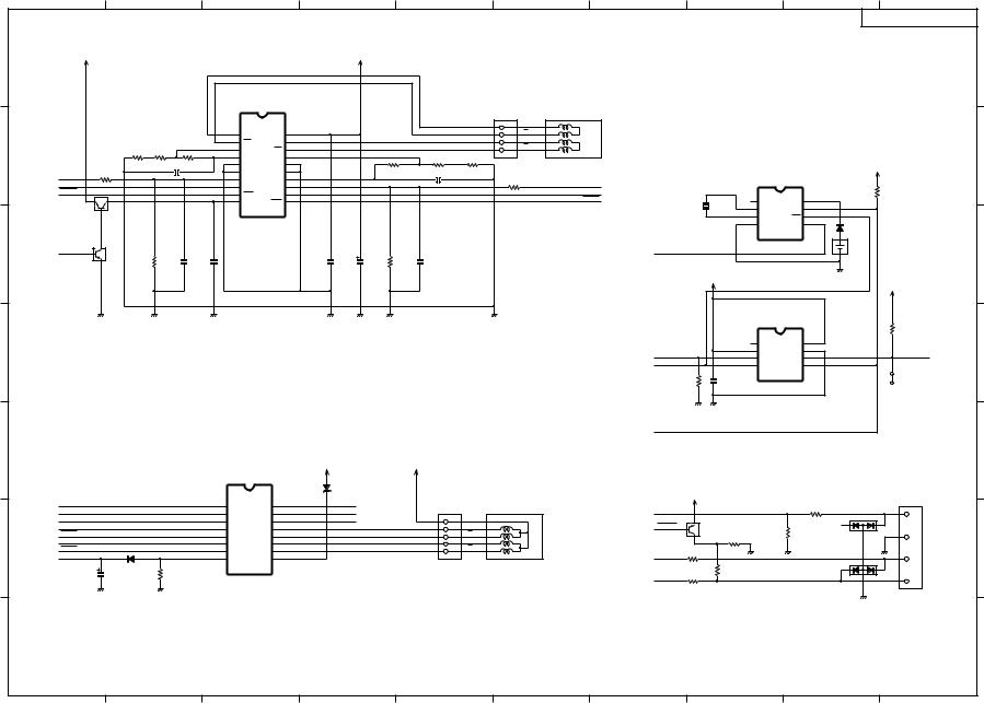
1 |
|
|
|
2 |
|
|
3 |
|
|
|
|
4 |
|
|
5 |
|
|
|
6 |
7 |
|
|
|
8 |
|
9 |
|
|
10 |
|
|
|
|
|
|
|
|
|
|
|
|
|
|
|
|
|
|
|
|
|
|
|
|
|
|
|
|
|
|
CONTROL PCB ASS'Y 05 |
|
|
|
Vcc1 |
|
|
|
|
|
|
|
|
|
|
Vpp |
|
|
|
|
|
|
|
|
|
|
|
|
|
|
|
A |
|
|
|
|
|
|
|
Carriage Motor Driver |
|
|
|
|
|
|
|
|
|
|
|
|
|
|
|
|
|
|
|
|||||
|
|
|
|
|
|
|
|
IC10 |
|
|
|
|
|
|
|
|
|
|
|
|
|
|
|
|
|
|
|
|
||
|
|
|
|
|
|
|
|
|
|
|
|
|
|
|
|
|
|
CNCR1 |
|
|
|
|
|
|
|
|
|
|
|
|
|
|
|
|
|
|
|
|
|
|
|
|
|
|
|
|
|
|
4 |
A |
|
|
|
|
|
|
|
|
|
|
|
|
|
|
|
|
|
|
1 |
OA |
|
VM |
20 |
|
|
|
|
|
|
3 |
A |
|
|
|
|
|
|
|
|
|
|
|
|
|
|
|
|
|
|
2 |
|
19 |
|
|
|
|
|
|
2 |
B |
|
approx.8.3 /phase |
|
|
|
|
|
|
|
|
|
||
|
|
|
R602 |
|
R603 |
|
OA |
|
OB |
|
|
|
|
|
|
|
|
|
|
|
|
|
|
|
|
|||||
|
|
|
|
|
3 |
|
18 |
|
|
|
|
|
|
1 |
B |
|
|
|
|
|
|
|
|
|
|
|
||||
|
|
|
0.39,1/2W |
0.39,1/2W |
|
SGA |
|
OB |
|
|
|
|
|
|
|
|
|
|
|
|
|
|
|
|
B |
|||||
|
|
|
|
4 |
|
17 |
|
|
|
|
R607 |
R608 |
|
|
|
|
|
|
|
|
|
|
|
|
||||||
|
|
|
|
|
|
|
Sen.A |
|
SGB |
|
|
|
|
|
|
|
|
|
|
|
|
|
|
|
|
|||||
|
|
|
|
|
C601 |
R604 |
5 |
|
16 |
|
|
|
|
0.39,1/2W |
0.39,1/2W |
|
|
|
|
|
|
|
|
|
|
|
|
|||
|
|
|
R601 |
|
GND |
|
GND |
|
|
|
|
|
Carriage Motor |
|
|
|
|
|
|
|
|
|
|
|||||||
|
|
|
|
|
|
|
|
|
|
|
|
|
|
|
|
|
Timer |
|
|
Vcc1 |
|
|||||||||
|
|
|
0.1μ,25V |
1.6K,1/16W |
6 |
|
15 |
|
|
R606 |
|
C604 |
|
|
|
|
|
|
|
|
|
|
||||||||
|
|
10K,1/16W |
1 |
|
4 |
|
|
|
|
|
|
|
|
|
|
|
|
|
|
|
||||||||||
|
|
|
|
|
7 |
|
14 |
|
|
1.6K,1/16W |
0.1μ,25V |
R609 |
|
|
|
|
|
|
|
IC |
|
|
|
|
||||||
<03-F3> |
CRREF1 |
|
|
|
|
GND |
|
GND |
|
|
|
|
|
|
|
|
|
|
|
|
|
|||||||||
<03-C2> |
ACRM |
|
|
|
|
|
8 |
2 |
|
3 |
13 |
|
|
|
|
|
|
10K,1/16W |
CRREF2 |
<03-F3> |
|
|
|
|
|
|
|
|
|
|
|
|
|
|
|
|
|
|
|
|
|
|
|
|
|
|
|
|
|
|
|
R612 |
|
||||||||
ACRM |
|
|
|
|
|
9 |
|
12 |
|
|
|
|
|
|
|
|
BCRM |
|
|
|
|
|
|
|
|
|||||
<03-C2> |
|
|
|
|
|
VrefA |
Sen.B |
|
|
|
|
|
|
|
|
<03-C2> |
|
|
|
|
|
|
|
10K,1/16W |
|
|||||
|
1 |
2 |
|
|
|
10 |
11 |
|
|
|
|
|
|
|
|
BCRM |
|
|
|
1 |
|
8 |
|
|
||||||
|
|
|
|
|
PhA |
VrefB |
|
|
|
|
|
|
|
|
<03-C2> |
|
|
|
vdd |
|
|
|
||||||||
|
|
|
|
|
|
|
|
|
|
|
|
|
|
|
|
|
|
|
X2 |
|
tpout |
7 |
|
|
|
|||||
|
|
|
|
|
|
|
|
|
|
|
|
|
|
|
|
|
|
|
|
|
|
|
|
2 |
sio |
|
|
|
||
|
|
|
|
|
|
|
|
|
|
|
|
|
|
|
|
|
|
|
|
|
|
|
|
|
xout |
6 |
|
|
|
|
|
|
3 |
Q12 |
|
|
|
|
|
|
|
|
|
|
|
|
|
|
|
|
|
|
|
|
|
3 |
sck |
|
|
|
|
|
|
|
|
|
|
|
|
|
|
|
|
|
|
|
|
|
|
|
|
|
|
|
xin |
5 |
|
|
|
|||
|
|
|
|
|
|
|
|
|
|
|
|
|
|
|
|
|
|
|
|
|
|
|
|
|
4 |
cs |
|
|
|
|
|
|
|
|
|
|
|
|
|
|
|
|
|
|
|
|
|
|
|
|
|
|
|
|
|
vss |
|
|
D5 |
|
|
|
|
|
|
|
|
|
|
|
|
|
|
|
|
|
|
|
|
|
|
|
|
|
|
|
|
|
|
|
|
|
|
|
2 |
R605 |
C602 |
C603 |
|
|
|
|
|
C605 |
C606 |
R610 |
C607 |
|
|
|
|
|
|
|
|
|
|
|
|
|
BATT1 |
C |
|
|
MTSTB |
3 |
15K,1/16W |
0.01μ,50V |
0.1μ,25V |
|
|
|
|
|
0.1μ,25V |
33μ,25V |
15K,1/16W |
0.01μ,50V |
|
|
|
|
|
|
T-OE |
|
|
|
|
|
|
|||
<02-A3> |
|
|
|
|
|
|
|
|
|
|
<02-F3> |
|
|
|
|
|
|
|
||||||||||||
|
|
Q19 |
|
|
|
|
|
|
|
|
|
|
|
|
|
|
|
|
|
|
|
|
|
|
|
|
|
|||
|
|
1 |
|
|
|
|
|
|
|
|
|
|
|
|
|
|
|
|
|
|
|
|
|
|
|
|
|
|
|
|
|
|
|
|
|
|
|
|
|
|
|
|
|
|
|
|
|
|
|
|
|
|
|
|
Vcc1 |
|
|
|
|
|
|
|
|
|
|
|
|
|
|
|
|
|
|
|
|
|
|
|
|
|
|
|
|
|
|
|
|
|
|
|
Vcc1 |
|
|
|
|
|
|
|
|
|
|
|
|
|
|
|
|
|
|
|
|
|
|
|
|
|
|
EEPROM(2K) |
|
|
|
||
19 |
|
|
|
|
|
|
|
|
|
|
|
|
|
|
|
|
|
|
|
|
|
|
|
|
|
IC9 |
|
|
R614 |
|
|
|
|
|
|
|
|
|
|
|
|
|
|
|
|
|
|
|
|
|
|
|
|
|
2 |
|
7 |
|
10K,1/16W |
|
|
|
|
|
|
|
|
|
|
|
|
|
|
|
|
|
|
|
|
|
|
|
|
|
|
|
1 |
NC2 |
8 |
|
|
|
|
|
|
|
|
|
|
|
|
|
|
|
|
|
|
|
|
|
|
|
|
|
|
|
|
NC1 |
|
|
|
D |
|
|
|
|
|
|
|
|
|
|
|
|
|
|
|
|
|
|
|
|
|
|
|
E-OE |
|
|
Vcc |
GND |
6 |
|
E-DO |
|
|
|
|
|
|
|
|
|
|
|
|
|
|
|
|
|
|
|
|
|
|
<03-F4> |
|
|
3 |
DO |
|
<03-D2> |
|||
|
|
|
|
|
|
|
|
|
|
|
|
|
|
|
|
|
|
|
|
|
TE-CLK |
|
|
CS |
5 |
|
|
|||
|
|
|
|
|
|
|
|
|
|
|
|
|
|
|
|
|
|
|
|
|
<03-F3> |
|
|
4 |
DI |
|
|
|
||
|
|
|
|
|
|
|
|
|
|
|
|
|
|
|
|
|
|
|
|
|
|
|
|
SK |
|
|
|
|
||
|
|
|
|
|
|
|
|
|
|
|
|
|
|
|
|
|
|
|
|
|
|
|
R613 |
|
R609 |
|
|
|
CP2 |
|
|
|
|
|
|
|
|
|
|
|
|
|
|
|
|
|
|
|
|
|
|
|
|
|
|
|
|
|
|
||
|
|
|
|
|
|
|
|
|
|
|
|
|
|
|
|
|
|
|
|
|
|
5.6K,1/16W |
|
0.01μ,50V |
|
|
|
CP1 |
|
|
|
|
|
|
|
|
|
|
|
|
|
|
|
|
|
|
|
|
|
|
|
<03-F3> |
TE-DIO |
|
|
|
|
|
|
|
|
|
|
|
|
|
|
|
|
|
|
|
|
|
|
|
|
|
|
|
|
|
|
|
|
|
|
|
|
|
|
|
|
|
|
|
|
|
|
|
|
|
|
|
|
|
|
|
|
|
|
|
|
|
|
|
|
|
|
|
|
|
E |
|
|
|
|
|
|
Paper Feed Motor Driver |
VH |
|
|
VH |
|
|
|
|
|
|
|
|
|
|
|
|
|
|
|
|||||
|
|
|
|
|
|
|
|
|
|
|
|
|
|
|
|
|
|
|
|
|
|
|
|
|
||||||
|
|
|
|
|
|
|
|
IC11 |
|
|
|
|
|
|
|
|
|
|
|
|
|
|
|
|
|
|
|
|
|
|
|
|
|
|
|
|
|
|
|
|
|
|
ZD4 |
|
|
|
|
|
|
|
|
|
|
3VCC |
|
|
|
|
|
USB Interface |
|
|
|
|
|
|
|
|
|
|
|
|
|
|
|
|
|
|
|
|
|
|
|
|
|
|
|
|
|
|
|
|
<02-A3> |
WHEAT |
|
|
|
|
1 |
I1 |
|
O1 |
16 |
|
|
W-HT |
<02-C7> |
|
|
|
|
|
|
|
|
|
|
|
|
R9 |
|
CNUS1 |
|
<02-A3> |
MCHE1 |
|
|
|
|
2 |
I2 |
|
O2 |
15 |
|
|
MCH1 |
<02-B7> |
|
CNLF1 |
|
|
|
|
<02-D1> |
PLUG |
|
|
|
|
10K,1/16W |
|
1 |
|
|
|
|
|
|
|
|
|
COM |
|
|
|
1 |
|
|
|
|
|
PWR |
||||||||||||
<02-A3> |
MCHE0 |
|
|
|
|
3 |
I3 |
|
O3 |
14 |
|
|
MCH0 |
<02-B7> |
|
1 |
|
|
|
|
|
|
|
|
|
3 |
4 |
|
||
ALFM |
|
|
|
|
4 |
|
13 |
|
|
|
|
5 |
A |
|
|
|
<02-D1> |
PULLUP |
3 |
Q1 |
|
R11 |
DA6 |
|
||||||
<03-C1> |
ALFM |
|
|
|
|
5 |
I4 |
|
O4 |
12 |
|
|
|
|
|
2 |
A |
|
|
|
|
|
R5 |
47K, |
HZM6.8FA |
|
4 |
|
||
<03-C1> |
|
|
|
|
I5 |
|
O5 |
|
|
|
|
|
|
|
|
|
|
|
|
|
|
GND |
||||||||
BLFM |
|
|
|
|
6 |
|
11 |
|
|
|
|
|
4 |
B |
|
|
approx.69.5 /phase |
|
|
2 |
|
47K,1/16W |
|
|
|
|
||||
<03-C2> |
|
|
|
|
I6 |
|
O6 |
|
|
|
|
|
|
|
|
|
|
|
1/16W |
|
|
|
F |
|||||||
BLFM |
|
|
|
|
7 |
|
10 |
|
|
|
|
|
3 |
B |
|
|
|
|
|
|
|
|
|
|
|
|
||||
<03-C2> |
LF-PRT |
|
|
|
|
8 |
I7 |
|
O7 |
9 |
|
|
|
|
|
|
|
|
|
|
|
USBD- |
|
|
|
|
|
|
2 |
|
<01-D10> |
|
|
|
|
GND |
|
COM |
|
|
|
|
|
|
|
Paper Feed Motor |
<02-D1> |
|
|
|
|
|
|
D- |
|||||||
|
|
|
D6 |
|
|
|
|
|
|
|
|
|
|
|
|
|
|
|
|
R7 |
|
R6 |
|
DA6 |
1 |
5 |
|
|||
|
|
C608 |
|
R611 |
|
|
|
|
|
|
|
|
|
|
|
|
|
|
|
|
|
24,1/16W |
|
1.5K,1/16W |
|
|
|
|
||
|
|
|
|
|
|
|
|
|
|
|
|
|
|
|
|
|
|
|
|
|
|
|
HZM6.8FA |
|
|
|
||||
|
1μ,50V |
|
|
0.68,1/2W |
|
|
|
|
|
|
|
|
|
|
|
|
|
|
<02-D1> |
USBD+ |
|
|
|
|
|
3 |
D+ |
|||
|
|
|
|
|
|
|
|
|
|
|
|
|
|
|
|
|
|
|
|
|
|
|
||||||||
|
|
|
|
|
|
|
|
|
|
|
|
|
|
|
|
|
|
|
|
|
|
|
|
|
||||||
|
|
|
|
|
|
|
|
|
|
|
|
|
|
|
|
|
|
|
|
|
|
|
R8 |
|
|
|
|
|
|
|
|
|
|
|
|
|
|
|
|
|
|
|
|
|
|
|
|
|
|
|
|
|
|
24,1/16W |
|
|
|
|
|
|
|

REVISION 0
|
|
|
Q30-3210-220 |
120V(CCSI) |
|
Q30-3210-221 |
120V(CANADA) |
|
Q30-3210-222 |
120V(LATIN) |
|
Q30-3210-230 |
220V-240V(EUR) |
|
Q30-3210-231 |
220V-240V(GER) |
|
Q30-3210-232 |
220V-240V(FRN) |
|
Q30-3210-233 |
220V-240V(ASIA HV) |
|
Q30-3210-240 |
220V-240V(AUST) |
|
Q30-3210-280 |
220V-240V(UK) |
|
Q30-3211-210 |
100V,50/60HZ(JPN) |
|
Q30-3212-250 |
220V-240V(HK) |
|
Q30-3212-260 |
220V-240V(KRN) |
|
|
|
|
NOV. 1999 |
QY8-31AJ-000 |
COPYRIGHT ã 1999 CANON INC. CANON BJC-85/BJ M70 1199 SE 0.25-0 PRINTED IN JAPAN (IMPRIME AU JAPON)
1199 SE 0.25-0

Application
This manual has been issued by Canon Inc. for qualified person to learn technical theory, installation, maintenance, and repair of products. This manual covers all localities where the products are sold. For this reason, there may be information in this manual that does not apply to your locality.
Corrections
This manual could include technical inaccuracies or typographical errors due to improvements or changes in the products. When changes occur in applicable products or in the content of this manual, Canon will release technical information as the need arises. In the event of major changes in the contents of this manual over a long or short period. Canon will issue a new editions of this manual.
The following paragraph does not apply to any countries where such provisions are inconsistent with local low.
Trademarks
The product names and company names described in this manual are the registered trademarks of the individual companies.
Copyright
This manual is copyrighted with all rights reserved. Under the copyright laws, this manual may not be copied, reproduced or translated into another language, in whole or in part, without the written consent of Canon Inc.
Copyright © 1999 by Canon Inc. CANON INC.
BJ Printer Technical Support Dept.
16-1, Shimonoge 3-chome, Takatsu-ku, Kawasaki-shi, Kanagawa 213-8512, Japan
DTP System
This manual was produced on an Apple® Power Macintosh® G3 personal computer and Canon LBP-2030PS laser beam printer, final pages were printed on Valityper® 4300J.
A Canon mo-5001S™ Magneto-optical Storage Subsystem with mo-502M™ Magneto-Optical Storage Disk Cartridge and mo-IF2™ Machitosh® interface kit were used for storing large volumes of page layout, graphic and parts list data for this manual.
Parts layout illustrations and Logotypes were created using MACROMEDIA® FreeHand® 7J.
Pattern drawing were scanned by CanoScan 600 scanner with Adobe® photoshop® .
Documents and page layouts were created using QuarkXpress® 3.3J.
Parts lists were created using Helix Tecnologies® Herix Xpress® and converted to EPS files.

I. CONTENTS
A.PARTS LAYOUT & PARTS LIST
B.SCREWS & WASHERS LIST
C.NUMERICAL INDEX
I

II. ABOUT THIS MANUAL
A PARTS LAYOUT & PARTS LIST
Parts layout illustration a) Parts search
Find a part from the parts layout illustration and find its key number from the parts list to identify the part number and name. For screws, nuts, washers, lock washers, pins, spacers, see SCREWS &WASHERS LIST.
Note: If parts have the same or similar shape but different specifications, their key number is assigned to several part numbers and names in the parts list.
b) Parts replacement procedure
To replace parts, the parts layout illustrations have figure numbers according to the disassembly procedure of the product. The parts that require careful work are shown the illustration.
Parts list
a) FIGURE & KEY No.
The FIGURE & KEY No. column corresponds to the key numbers assigned to the parts in the parts layout illustration.
It also corresponds to the part locations printed on the PC board.
b) PART NUMBER
The PART NUMBER column gives the part numbers corresponding to the key numbers. To order a part, indicate the part number clearly.
Note: Parts marked NPN are not service parts.
c) RANK
The service parts with N in the RANK column are order parts.
d) QTY
The QTY column gives the number of parts in the corresponding components layout illustration.
e) DESCRIPTION
The DESCRIPTION column gives the part names in English.
To order a part, indicate the part name, too.
TOOL LIST
This is a list of tools used for servicing products.
B. SCREWS & WASHERS LIST
This is a list of screws, nuts, washers, lock washers, pins, and spacers.
The QTY column does not give the number of parts used.
C. NUMERICAL INDEX
All the parts listed in this parts catalog are arranged in order of part number. You can identify part locations and names from the NUMERICAL INDEX.
II
III

A. PARTS LAYOUT & PARTS LIST
FIGURE 1 |
PRINTER SET |
FIGURE 2 |
TOP COVER |
|
|
|
|
||
|
1 |
|
|
|
|
|
3 |
|
|
|
2 |
4 |
|
|
|
|
|
|
|
|
|
5 |
|
|
6 |
|
|
|
|
7 |
|
8 |
|
|
|
|
|
|
|
|
|
2 |
|
|
|
UPPER COVER |
|
CONTROL BOARD & |
|
FIGURE 3 |
FIGURE 4 |
LOWER COVER |
|
|
|
|
|||
|
2 |
|
|
|
|
|
|
2 |
|
|
|
1 |
|
|
|
|
|
1 |
|
|
|
|
S2 |
|
|
4 |
|
S2 |
3 |
|
3 |
|
|
|
|
|
|
S2 |
|
|
|
|
|
4 |
|
|
|
5 |
|
|
|
|
6 |
|
|
|
|
8 |
7 |
|
|
|
|
|
|
|
|
9 |
|
|
|
|
8 |
|
|
S1 |
|
|
|
|
|
A-1 |
|
|
 Loading...