

Page 1
h
MAINTENANCE MANUAL
KY 96A, KY 97A
VHF COMMUNICATION
MANUAL NUMBER 006-05674-0005
TRANSCEIVER
Revision 5, April 2003
Page 2

WARNING
THE ENCLOSED TECHNICAL DATA IS ELIGIBLE FOR EXPORT UNDER LICENSE
DESIGNATION NLR AND IS TO BE USED SOLELY BY THE INDIVIDUAL/ ORGANIZATION TO WHOM IT IS ADDRESSED. DIVERSION CONTRARY TO U.S. LAW IS PROHIBITED.
COPYRIGHT NOTICE
©1989, 1992, 1994, 1997, 2003 HONEYWELL INTERNATIONAL INC.
REPRODUCTION OF THIS PUBLICATION OR ANY PORTION THEREOF BY ANY
MEANS WITHOUT THE EXPRESS WRITTEN PERMISSION OF HONEYWELL IS
PROHIBITED. FOR FURTHER INFORMATION CONTACT THE MANAGER, TECHNICAL
PUBLICATIONS, HONEYWELL, ONE TECHNOLOGY CENTER, 23500 WEST 105TH
STREET OLATHE KS 66061 TELEPHONE: (913) 782-0400.
Page 3

B KY 96A, KY 97A
REVISION HISTORY
MAINTENANCE MANUAL
BENDIX/KING
KY 96A, KY 97A
VHF Communication Transceiver
PART NUMBER REV DATE DESCRIPTION
--------------------------------------------------------------------------------------------------------------------006-05674-0005 5 Apr/2003 Incorporated -0020 SW/HW versions.
006-05674-0004 4 Apr/1994 Incorporated IM Rev 3.
006-05674-0003 3 Jan/1994 Revised Section VI.
Incorporated IM Rev 2.
006-05674-0002 2 Oct/1992 Revised Section VI.
006-05674-0001 1 Oct/1989 Incorporated IM Rev 1.
Rev 5, Apr 2003 MM 006-05674-0005.dwd RH-1
Page 4

B KY 96A, KY 97A
THIS PAGE RESERVED
Rev 5, Apr 2003 MM 006-05674-0005.dwd RH-2
Page 5

B TABLE OF CONTENTS KY 96A, KY 97A
SECTION IV
THEORY OF OPERATION
Paragraph Page
4.1 General....................................................................................................4-1
4.2 General Circuit Theory.............................................................................4-1
4.3 Detailed Theory of Operation...................................................................4-3
LIST OF ILLUSTRATIONS
Figure Page
4-1 Receiver Block Diagram ........................................................................4-13
4-2 Transmitter Block Diagram ....................................................................4-15
4-3 Microprocessor Block Diagram..............................................................4-17
SECTION V
MAINTENANCE
Paragraph Page
5.1 General Information.................................................................................5-1
5.2 Test Equipment........................................................................................5-1
5.3 Performance Test Procedure...................................................................5-4
5.4 Alignment Procedure ...............................................................................5-9
5.5 Overhaul ................................................................................................5-11
LIST OF TABLES
Table Page
5-1 Required Test Equipment........................................................................5-1
5-2 Optional Test Equipment .........................................................................5-2
LIST OF ILLUSTRATIONS
Figure Page
5-1 Typical Test Equipment Setup................ ................................................5-3
5-2 Linear Detector....................................... ..............................................5-13
5-3 MIC Test Circuit...................................... ..............................................5-13
5-4 40 dB Antennuator.................................. ..............................................5-14
5-5
Bench Test Harness.................................. ..............................................5-15
Rev 5, Apr 2003 MM 006-05674-0005.dwd TOC-1
Page 6

B TABLE OF CONTENTS KY 96A, KY 97A
SECTION VI
ILLUSTRATED PARTS LIST
Paragraph Page
6.1 Introduction..............................................................................................6-1
6.2 Bill of Material Description .......................................................................6-1
6.3 Software Documentation .........................................................................6-9
6.4 Illustrated Parts List ...............................................................................6-17
6.4.1 KY 96A VHF Communication Transceiver.............................................6-17
6.4.2 KY 97A VHF Communication Transceiver.............................................6-41
6.4.3 KY 96A, KY 97A Unit Software Set .......................................................6-53
6.4.4 LCD Processor Board............................................................................6-57
6.4.5 KY 97A (14V) Modulator Assembly .......................................................6-71
6.4.6 KY 96A (28V) Modulator Assembly .......................................................6-79
6.4.7 LCD Display Board ................................................................................6-87
6.4.8 Transmitter Board................................................................................6-105
6.4.9 Audio Amplifier Board..........................................................................6-135
6.4.10 Main Board ..........................................................................................6-149
LIST OF TABLES
Table Page
6-1 Reference Designator Abbreviations.......................................................6-1
6-2 Description Abbreviations........................................................................6-3
6-3 Unit of Measure Abbreviations.................................................................6-9
LIST OF ILLUSTRATIONS
Figure Page
6-0 Sample Parts List.................................... ..............................................6-13
6-1 KY 96A Final Assembly ..........................(Dwg 300-04268-0000).........6-25
6-1A KY 96A Final Assembly ..........................(Dwg 300-04268-0000).........6-29
6-1B KY 96A Final Assembly ..........................(Dwg 300-04268-0000).........6-33
6-1C KY 96A Final Assembly ..........................(Dwg 300-04268-0000).........6-37
6-2 KY 97A Final Assembly ..........................(Dwg 300-04268-0001).........6-49
6-3 LCD Processor Board Assembly ............(Dwg 300-07475-0000).........6-61
6-3A LCD Processor Board Assembly ............(Dwg 300-07475-0000).........6-63
6-4 LCD Processor Board Schematic...........(Dwg 002-07475-0000).........6-65
6-4A LCD Processor Board Schematic...........(Dwg 002-07475-0000).........6-67
6-4B LCD Processor Board Schematic...........(Dwg 002-07475-0000).........6-69
6-5 KY 97A (14V) Modulator Assembly ........(Dwg 300-04270-0000).........6-75
6-5A KY 97A (14V) Modulator Assembly ........(Dwg 300-04270-0000).........6-77
6-6 KY 96A (28V) Modulator Assembly ........(Dwg 300-04271-0000).........6-83
Rev 5, Apr 2003 MM 006-05674-0005.dwd TOC-2
Page 7

B TABLE OF CONTENTS KY 96A, KY 97A
6-6A KY 96A (28V) Modulator Assembly ........(Dwg 300-04271-0000).........6-85
6-7 LCD Display Board Assembly.................(Dwg 300-07479-0000).........6-91
6-7A LCD Display Board Assembly.................(Dwg 300-07479-0000).........6-93
6-7B LCD Display Board Assembly.................(Dwg 300-07479-0000).........6-95
6-7C LCD Display Board Assembly.................(Dwg 300-07479-0000).........6-97
6-8 LCD Display Board Schematic ...............(Dwg 002-07479-0000).........6-99
6-8A LCD Display Board Schematic ...............(Dwg 002-07479-0000).......6-101
6-8B LCD Display Board Schematic ...............(Dwg 002-07479-0000).......6-103
6-9 KY 97A (14V) Transmitter Assembly......(Dwg 300-07540-0000).......6-109
6-9A KY 97A (14V) Transmitter Assembly......(Dwg 300-07540-0000).......6-111
6-9B KY 97A (14V) Transmitter Assembly......(Dwg 300-07540-0000).......6-113
6-10 KY 97A (14V) Transmitter Schematic.....(Dwg 002-07540-0000).......6-115
6-10A KY 97A (14V) Transmitter Schematic.....(Dwg 002-07540-0000).......6-117
6-10B KY 97A (14V) Transmitter Schematic.....(Dwg 002-07540-0000).......6-119
6-11 KY 96A (28V) Transmitter Assembly......(Dwg 300-07540-0001).......6-121
6-11A KY 96A (28V) Transmitter Assembly......(Dwg 300-07540-0001).......6-123
6-11B KY 96A (28V) Transmitter Assembly......(Dwg 300-07540-0001).......6-125
6-12 KY 96A (28V) Transmitter Schematic.....(Dwg 002-07540-0001).......6-127
6-12A KY 96A (28V) Transmitter Schematic.....(Dwg 002-07540-0001).......6-129
6-12B KY 96A (28V) Transmitter Schematic.....(Dwg 002-07540-0001).......6-131
6-12C KY 96A (28V) Transmitter Schematic.....(Dwg 002-07540-0001).......6-133
6-13 Audio Amplifier Board Assembly ............(Dwg 300-07797-0000).......6-139
6-13A Audio Amplifier Board Assembly ............(Dwg 300-07797-0000).......6-141
6-14 Audio Amplifier Board Schematic ...........(Dwg 002-07797-0000).......6-143
6-14A Audio Amplifier Board Schematic ...........(Dwg 002-07797-0000).......6-145
6-14B Audio Amplifier Board Schematic ...........(Dwg 002-07797-0000).......6-147
6-15 KY 97A (14V) Main Board Assembly......(Dwg 300-07799-0000).......6-199
6-15A KY 97A (14V) Main Board Assembly......(Dwg 300-07799-0000).......6-203
6-15B KY 97A (14V) Main Board Assembly......(Dwg 300-07799-0000).......6-207
6-15C KY 97A (14V) Main Board Assembly......(Dwg 300-07799-0000).......6-211
6-16 KY 96A (28V) Main Board Assembly......(Dwg 300-07799-0001).......6-215
6-16A KY 96A (28V) Main Board Assembly......(Dwg 300-07799-0001).......6-219
6-16B KY 96A (28V) Main Board Assembly......(Dwg 300-07799-0001).......6-223
6-16C KY 96A (28V) Main Board Assembly......(Dwg 300-07799-0001).......6-227
6-17 KY 96A, KY 97A Main Board Schem......(Dwg 002-07799-0000).......6-231
6-17A KY 96A, KY 97A Main Board Schem......(Dwg 002-07799-0000).......6-249
6-17B KY 96A, KY 97A Main Board Schem......(Dwg 002-07799-0000).......6-261
Rev 5, Apr 2003 MM 006-05674-0005.dwd TOC-3
Page 8

B TABLE OF CONTENTS KY 96A, KY 97A
APPENDIX S
SOFTWARE/ HARDWARE CONFIGURATION
LIST OF ILLUSTRATIONS
Figure Page
S-1 KY 96A Software/ Hardware Configuration ............................................ S-3
S-2 KY 97A Software/ Hardware Configuration ............................................ S-9
Rev 5, Apr 2003 MM 006-05674-0005.dwd TOC-4
Page 9

B KY 96A, KY 97A
SECTION IV
THEORY OF OPERATION
4.1 GENERAL
The KY 96A, KY 97A Comm Transceiver is comprised of:
A. A single conversion VHF receiver utilizing a four pole varactor tuned prese-
lector, field effect transistors for the RF amplifier and mixer, an 8 pole monolithic crystal IF filter and integrated circuit IF amplifier.
B. A broadband transmitter with power transistors mounted on a die-cast alu-
minum heat sink followed by a three section elliptic function low pass filter.
C. A control section utilizing a microprocessor to:
1. Increment or decrement the selected frequency.
2. Store the “USE,” “STBY,” and 9 user programmable channels in non-volatile memory.
3. Remote transfer the “USE” and “STBY” frequencies and remote increment
the stored channels.
4. Light the display with a digital liquid crystal readout and control dimming of
the display.
5. Generate frequency code for the synthesizer.
D. A power supply made up of a discrete 9 volt regulator, 3 terminal 5 volt reg-
ulator.
E. A liquid crystal frequency display with variable backlighting and viewing an-
gle.
4.2 GENERAL CIRCUIT THEORY
4.2.1 Receiver
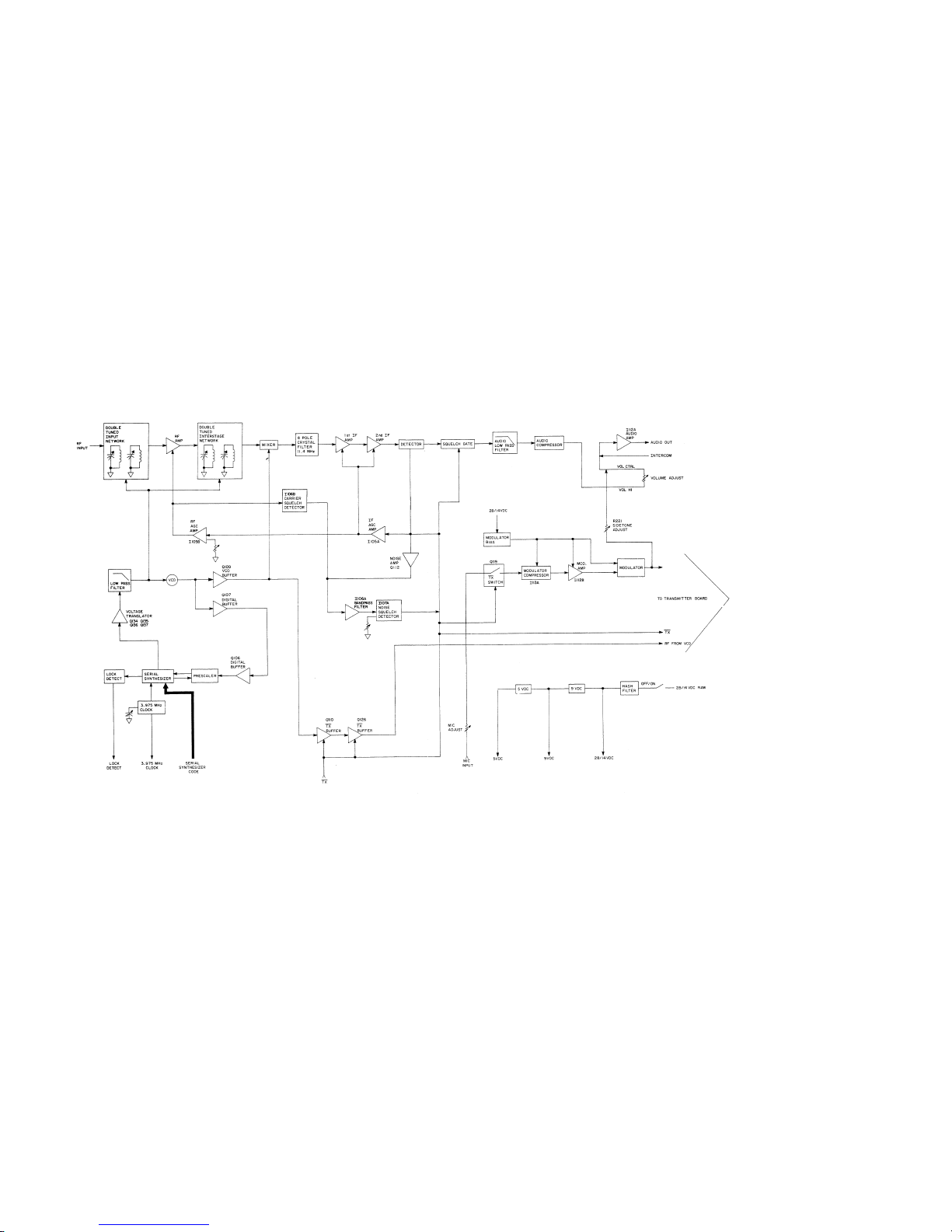
A receiver block diagram is shown in Figure 4-1. The received signal passes through
the low pass filter on the transmitter PC board and the T/R diode to the dual gate field
effect transistor RF amplifier. The desired signal proceeds to the dual gate FET mixer
Q103 where it is converted to 11.4 MHz, and fed through the monolithic crystal filter to
the integrated circuit IF amplifiers followed by the detector. Automatic gain control
voltage is fed back to the first and second IF amplifiers and the RF amplifier to achieve
more than 120 dB of dynamic range. The detected signal is not allowed to pass
through the squelch gate until the input signal has:
A. Exceeded the noise squelch setting or,
B. Exceeded the carrier level setting.
Rev 5, Apr 2003 MM 006-05674-0005.dwd Page 4-1
Page 10

B KY 96A, KY 97A
It proceeds through the low pass filter which attenuates all audio frequencies above
2.5 kHz. The audio signal is fed through the volume control to the integrated circuit
audio pre-amplifier. Its output will provide more than 100 milliwatts to a headphone,
or to an external audio mixer/amplifier.
An optional 4 ohm audio amplifier provides 4 watts on the 13.75 V units and 8 watts
on the 27.5 V units.
4.2.2 Transmitter/ Modulator
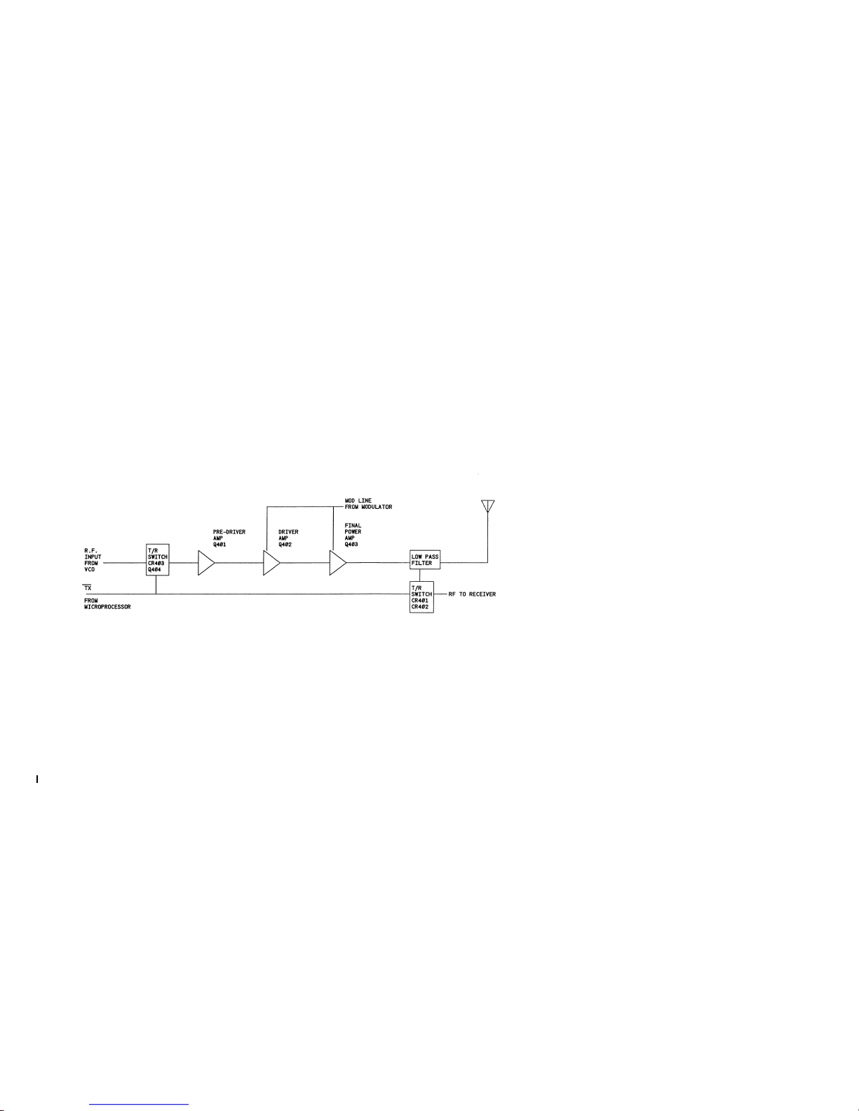
The transmitter block diagram is shown in Figure 4-2. In the transmit mode, the VCO
feeds a signal to the transmitter of the frequency selected in the “USE” display window
on the front panel. The signal is amplified by the broadband transmitter to the 5 watts
level and fed through the elliptic function 3 section low pass filter to the antenna.
Modulation is applied to the power amplifier by series modulating the 27.5 volt line
(13.75 for KY 97A) with mic audio. A small amount of mic audio is also fed to the receiver audio amplifier for sidetone.
4.2.3 Stabilized Master Oscillator
The stabilized master oscillator (SMO) I103 generates the RF drive for the transmitter
as well as the local oscillator for the receiver. The SMO synthesizes frequencies that
are referenced to a 25 kHz signal derived from a 3.975 MHz crystal oscillator. Receive
and transmit codes are fed to the synthesizer by the microprocessor (uP) and represent the frequency indicated in the “USE” window on the front panel.
4.2.4 Microprocessor and Display
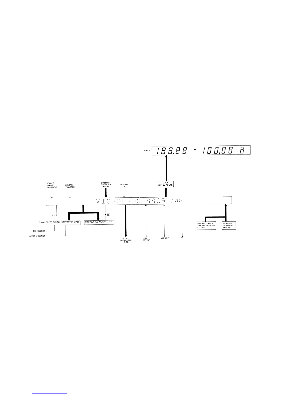
Refer to microprocessor block diagram shown in Figure 4-3. The microprocessor (uP)
contains 4 k bytes of permanent Read Only Memory (ROM) for program instruction. A
32 byte non-volatile memory is used externally for frequency information storage. The
uP receives a 3.975 MHz clock signal from the synthesizer PLL IC which is derived
from a 3.975 MHz crystal.
The uP sends a serial 24 bit code to the synthesizer PLL IC (last 20 bits used) to determine the reference divide ratio. A serial 24 bit code (last 20 bits used) is also sent
to determine the divide ration of the “USE” frequency (when changed).
The increment/decrement switches send three pulses to the uP (up, pulse, down) in a
specific sequence to provide the code and validity check for increment and decrement
operations.
Display dimming controls are read through an analog to digital converter allowing the
aircraft lighting bus to dim the display.
The LCD display viewing angle is controlled by I801, which controls the display bias,
thereby controlling the display viewing angle based on inputs from R755, R802, and
Q803.
Rev 5, Apr 2003 MM 006-05674-0005.dwd Page 4-2
Page 11

B KY 96A, KY 97A
4.3 DETAILED THEORY OF OPERATION
Refer to schematics in Section VI of this manual.
4.3.1 Receiver
4.3.1.1 Antenna Input Circuit
In the receive mode Q101 is switched on, forward biasing the T/R diodes located on
the transmitter board. The desired signal passes through the first pole of the low pass
filter, then to the T/R diodes, and then to the receiver board. C102 steps up the impedance to match the first pole of the preselector.
4.3.1.2 Double Tuned Preselector
The first pole of the preselector is tuned by L101, C103 and CR101A. The signal is
coupled to the second pole of the preselector by L102. The second pole of the preselector is tuned by L103, C106 and CR101B. The matched varactor diodes, CR101A
and CR101B, are tuned to the desired frequency through a large resistor from the VCO
control voltage. The desired signal is coupled to gate 1of the RF amplifier by C107.
4.3.1.3 RF Amplifier Q102
Q102 and the associated parts make up the RF amplifier. The desired signal is applied to gate 1. The RF AGC is applied to gate 2. The RF amplifier has 20 dB of gain
at maximum RF AGC voltage, and 30 dB of attenuation with minimum RF AGC voltage; producing a dynamic range of 50 dB. C114 couples the desired signal to the double tuned interstage.
4.3.1.4 Double Tuned Interstage Network
The first pole of the interstage network is tuned by L105, C115 and CR101C. The signal is coupled to the second pole of the interstage network by L106. The second pole
of the preselector is tuned by L107, C118 and CR101D. The matched varactor diodes,
CR101C and CR101D, are tuned to the desired frequency through a large resistor
from the VCO control voltage. The desired signal is coupled to gate 1 of the mixer
through L133.
4.3.1.5 Mixer Q103
Q103 and the associated parts make up the mixer. The local oscillator signal is fed to
gate 2 at a frequency 11.4 MHz above the desired signal. The level of the local oscillator is between +4 dBm and +7 dBm. The desired signal is now at 11.4 MHz. The
drain of Q103 is tuned to 11.4 MHz by T101 and matched to the crystal filter.
4.3.1.6 Crystal Filter FL101
The crystal filter provides the desired selectivity. The input and output of the filter is
matched to 4100 ohms by T101 and T102 respectively.
4.3.1.7 First IF Amplifier I101
Rev 5, Apr 2003 MM 006-05674-0005.dwd Page 4-3
Page 12

B KY 96A, KY 97A
The desired signal is coupled from T102 to the first IF amplifier, I101. The first IF amplifier has about 45 dB of gain with 60 dB of dynamic range. IF AGC voltage is applied
to I101 on pin 5 through R124. R124 converts the AGC voltage to an AGC current.
The output is loaded with R245 for stability. T103 is tuned for 11.4 MHz and couples
the signal to the second IF amplifier.
4.3.1.8 Second IF Amplifier I102
The second IF amplifier has about 45 dB of gain with 60 dB of dynamic range. IF AGC
voltage is applied to I102 on pin 5 through R126. R126 converts the AGC voltage to
an AGC current. The output is loaded with R246 for stability. T104 is tuned for 11.4
MHz and couples the signal to the detector.
4.3.1.9 Detector
Transistor Q105 and capacitor C130 makes up the amplitude modulation detector. It
is biased near cutoff by transistor Q104, which the emitter-base junction provides bias
stability and temperature compensation. The demodulated signal is sent to the noise
amp, Q112, IF AGC, I105A, squelch gate, Q116, and to the demodulator buffer, Q131.
4.3.1.10 IF AGC Circuit
AGC voltage is derived from the average value of the detector collector voltage, which
is inversely proportional to the carrier level. The operational amplifier I105A filters out
the audio variations and integrates to the average voltage of the detector. R159 and
R160 set the maximum gain reduction at about 6.6 volts. As the detector collector voltage increases with a decrease in signal level, the AGC voltage decreases which increases the gain in the first and second IF amplifiers. The IF AGC voltage is made
available at TP105 and at the rear connector pin L. The AGC voltage at pin L is reduced by one diode drop (approx. 0.6 V).
4.3.1.11 RF AGC Circuit
The RF AGC voltage is applied to the RF amplifier from I105B. The RF AGC stays at
maximum voltage (maximum gain of amp) until the RF signal level reaches about 12.5
uV. The level at which it attacks is set by R184. When the IF AGC voltage exceeds
the reference voltage set by R184, the RF AGC voltage decreases, decreasing the
gain in the RF amplifier. RF AGC is made available at TP106.
The RF AGC is gated with TX(not) through CR120A such that when the unit transmits,
the RF AGC voltage goes to zero. This provides maximum attenuation in the RF amplifier during transmit.
4.3.1.12 Noise and Carrier Squelch Circuit
The carrier squelch circuit prevents the radio from squelching if an RF carrier greater
than 12.5 uV has been detected. I106B compares the RF AGC voltage, which is inversely proportional to the carrier level, to the reference level set by R183 and R185.
If the RF AGC voltage is greater than the reference level, then the unit is allowed to
squelch; if the noise level is large enough. When the RF AGC voltage is less than the
reference level, the output of I106B goes high; turning on Q140. When Q140 turns on,
Rev 5, Apr 2003 MM 006-05674-0005.dwd Page 4-4
Page 13

B KY 96A, KY 97A
the input signal to the noise amp is shorted to ground, causing the noise squelch circuit
to be inhibited.
Transistor Q112 amplifies the noise from the collector of the detector and limits its amplitude so that impulse spikes (such as ignition noise) will not be of a higher amplitude
than other noise. The output of Q112 is coupled to a 8 to 10 kHz bandpass filter,
I106A. The output of the bandpass filter is fed to the comparator, I107A. The signal
is compared to the reference level set by R176. When the noise signal is larger than
the reference level the comparator goes high charging C166. If C166 is charged greater than half the supply voltage, then the unit will be squelched.
CR107A and CR110B will squelch the radio in transmit.
4.3.1.13 Squelch Gate
Q116, Q117 and associated parts make up the squelch gate. The audio signal comes
from the detector at TP108; the detector biases Q116. When the unit is squelched the
base of Q117 goes to the supply voltage and its emitter follows. Since the emitters of
Q116 and Q117 are tied together, Q116 becomes reverse biased; attenuating the signal 70 dB.
4.3.1.14 Audio Low Pass Filter
Inductor L110 and its associated capacitors form a low pass elliptical filter. The filter
is at least 20 dB down at 4 kHz and the notch is at least 25 dB down at 4.5 kHz. The
filter does roll off below 350 Hz since the signal is AC coupled in and out of the filter.
The low frequency roll off reduces 60 cycle hum.
4.3.1.15 Audio Compressor
The received signal is coupled through C178 to the input of the compressor amplifier,
I111A. The output is fed to the volume control and to I111B. I111B will begin to discharge C179 when the amplitude to I111B exceeds the voltage across R210. Discharging C179 lowers the gate to source voltage on Q118, which reduces the drain to
source resistance on Q118. As Q118 is turned on, the amplitude at C178 is reduced.
This maintains a constant amplitude out of the compressor amplifier.
4.3.1.16 Audio Amplifier
The audio signal is routed through the volume control R902 to the audio amplifier,
I112A. The signal is amplified approximately 30 dB and capacitive coupled through
C187 to the auto-transformer, T107. The voltage and impedance are stepped up to
provide a minimum of 100 mW of audio power into 500 ohm load; such as headphones
or an audio panel. The sidetone, through R220, and the Mic intercom, through R218,
are also amplified by the audio amplifier.
An optional 4 ohm audio amplifier provides 4 watts on 13.75 V units and 8 watts on
27.5 V units. See audio board section for more details.
4.3.2 Stabilized Master Oscillator (SMO)
Rev 5, Apr 2003 MM 006-05674-0005.dwd Page 4-5
Page 14

B KY 96A, KY 97A
4.3.2.1 Synthesizer
The stabilized master oscillator is based around synthesizer I103 which is serial programmable by the microprocessor.
A 3.975 MHz crystal is attached to the gate oscillator, and the reference divider divides
it by 159 to produce the 25 kHz reference frequency. The RF frequency is divided by
the internal pre-scaler and divider then compared by the phase detector to the reference frequency. If the frequency is greater than 25 kHz the phase detector will pulse
up once every 40 usec. If the frequency is less than 25 kHz the phase detector will
pulse down. The greater the divided frequency from the reference frequency the wider
the phase detector pulse.
Q133, R137, and C135 integrates the lock detect pulses to send the lock detect signal
to the microprocessor. The reference oscillator is lightly coupled to Q132 which amplifies the 3.975 MHz signal for the microprocessor and I705 on the processor board.
The clock, data and strobe lines are driven from the microprocessor.
4.3.2.2 Voltage Translator
Q134, Q135, Q136, Q137 and their associated parts make up the voltage translator.
The voltage translator translates from five volt pulse to nine volt pulse and inverts the
logic of the pulses. The output of the phase detector is fed to the emitters of Q134 and
Q135. The bases of Q134 and Q135 are biased to about 2 volts so that when the
phase detector is tri-stated, Q134 and Q135 will be off. If the phase detector pulses
low, Q134 will turn on causing Q136 to turn on and a 9 volt pulse to appear at the output of the voltage translator, TP110. If the phase detector pulses high, Q135 will turn
on causing Q137 to turn on pulling the output to ground.
4.3.2.3 Low Pass Filter
The low pass filter is a lead/ lag network with a 2.5 kHz elliptical low pass filter with its
notch at 25 kHz. C235 and C236 make up the elliptical filter. R279, R280, R281, and
C237 make up the lead/ lag network. With this filter, the loop bandwidth is about 300
Hz and the 25 kHz notch is about 130 dB down. The control voltage is fed to the preselector through R136 and to the VCO through L132.
4.3.2.4 Voltage Controlled Oscillator (VCO)
Q108 and its associate parts form a modified Hartley oscillator. The varactor CR101E
is part of a matched set of five varactors so the preselector will track the VCO. C149
determines the range of the tuning voltage, the smaller the capacitor the larger the tuning range must be to maintain the same frequency range. C249 and R299 provide
bias stability. The tuning range is 118.00 MHz at 2.5 V and 151.375 MHz at 8.0 V.
4.3.2.5 VCO Buffer
Q109 and its associated parts form the VCO buffer. The VCO buffer provides isolation
from the transmit buffers and the mixer as well as amplifying the signal to about +7
dBm to the mixer.
Rev 5, Apr 2003 MM 006-05674-0005.dwd Page 4-6
Page 15

B KY 96A, KY 97A
4.3.2.6 Digital Buffer
Q106, Q107 and their associated parts form the digital buffers. The VCO is very lightly
coupled to the digital buffers through C147 so that noise from the pre-scaler will not
get back to the VCO. The signal is coupled to the pre-scaler through C140 at about
500 mV.
4.3.2.7 Transmit Buffers
The transmit buffers contain two stages of amplification. The RF signal is coupled
through C155 to Q110 and amplified. C157 couples the collector of Q110 to Q126.
Q126 amplifies the signal to approximately 24 dBm. The signal is coupled through
CR117 and C228 to create the transmit drive. The drive level is adjusted for different
transmitters by the resistor R1006. Q111 and Q139 are turned off during receive allowing Q110 and Q126 to be reversed biased. Q127 is also turned off during receive
preventing CR117 from being turned on. During receive the RF signal is reduced by
50 dB.
4.3.3 Modulator
4.3.3.1 Microphone Input Circuit
The microphone is connected to pin K of the rear panel connector. Mic bias is supplied
by R114 and R223. The signal passes through C191 to the Mic Gain control. Q119
is turned on during transmit to pass the signal to the modulator compressor.
4.3.3.2 Modulator Compressor
The audio signal is coupled through C230 to the input of the compressor amplifier,
I113A. The output is fed to the modulator amplifier, I113B will begin to discharge C198
when the output of the modulator exceeds the voltage across R267. Discharging
C198 lowers the gate to source voltage on Q120, which reduces the drain to source
resistance on Q120. As Q120 is turned on the amplitude at C230 is reduced. This
maintains a constant amplitude out of the compressor amplifier. R267 set the modulation level. The bias network R257 and R267 is run off of the mod bias voltage, so
that when the mod bias sags the modulation will decrease preventing distortion.
4.3.3.3 Modulator Amplifier
The output of the compressor amplifier is coupled to the modulator amplifier through
C194. The output is coupled to the modulator through C196 and T108.
4.3.3.4 Modulator Bias
The modulator bias (mod bias) regulates the supply voltage to just below half the supply voltage. Q123 is the regulating transistor and on the 28 volt versions Q122 is used
to buffer the regulating transistor. The KY 96A drops the modulator bias an additional
6.2 volts through CR123. R251, R254, and R256 set the regulated voltage, with R256
being adjustable. CR115 prevents overvoltage problems. RT101, R250, and R252
set the power reduction due to a thermal overload. When RT101 becomes hot, the
resistance goes up reducing the voltage at E113, causing CR114 to turn on, and thus
lowers the bias on Q123.
Rev 5, Apr 2003 MM 006-05674-0005.dwd Page 4-7
Page 16

B KY 96A, KY 97A
4.3.3.5 Modulator (14 Volts KY 97A)
The audio signal is applied to the primary of T108, which has a 4 to 1 turns ratio. This
steps up the voltage swing on the modulator transistors Q124 and Q125 enough to
make a 0 to 12 V swing to the transmitter final and driver. This output is also fed back
to the modulator compressor. The mod bias is fed to the secondary of T108 providing
the bias to Q125 with R247 being the current limit resistor.
4.3.3.6 Modulator (28 Volts KY 96A)
The audio signal is applied to the primary of T108, which has a 4 to 1 turns ratio. This
steps up the voltage swing to the bases of the modulator transistors Q124 and Q130
enough to make a 1 to 12 V swing on the transmitter final and driver. This output is
also fed back to the modulator compressor. The mod bias is fed to the secondary of
T108 providing the bias to Q124 and Q130 with R247 being the current limit resistor.
4.3.4 Transmitter
4.3.4.1 RF Amplifier
RF is fed from the transmit buffers to the RF amp, on the transmitter board, through a
miniature 50 ohm coaxial cable. The drive level is approximately 15 dBm. During receive the RF is attenuated as the TX(not) line goes high it turns on Q404 shorting the
drive to ground and removing the bias from pin diode CR403 to “OPEN” the input to
Q401. During transmit, the base current is supplied through R401 and CR403 to operate Q401 class A. Transformer T401 is broadband tuned and steps the collector impedance down to the input impedance of the driver.
4.3.4.2 Driver Q402
RF drive is fed through C412 and C437 to the driver, Q402. The driver is operated
class C and the collector is modulated through T402. The collector is broadband tuned
and is coupled to the final by T402.
4.3.4.3 Final
Capacitor C415, C416, and C440 form the input matching network for the final power
amplifier, Q403. The final is operated class C and is modulated at the collector. The
low collector output impedance is stepped up to approximately 50 ohms by transformer T403.
4.3.4.4 Low Pass Filter
A three section elliptical low pass filter is placed between the final and the antenna to
attenuate all harmonics which may be generated in the transmitter. During transmit
the T/R diodes CR401 and CR402 are reversed biased to protect the receiver from 5
watts of power.
4.3.5 Microprocessor
4.3.5.1 Communication to Synthesizer PLL I702
Rev 5, Apr 2003 MM 006-05674-0005.dwd Page 4-8
Page 17

B KY 96A, KY 97A
The microprocessor (uP), pin 32, sends two 24 bit serial data streams to the synthesizer PLL IC (I103) on the main board. Only the last 20 bits are used by the synthesizer PLL IC. The first stream provides the crystal divide ration and the second provides the frequency to be divided. Each data bit is clocked from pin 33 of the uP. At
the end of each data stream, a high going strobe pulse is sent from pin 28 of the uP to
latch the last 20 bits of data into the synthesizer PLL IC.
When the synthesizer is locked, pin 25 (Lock Detect) of uP is pulled high from the synthesizer PLL IC I103. If pin 29 (Mic key(not)) of uP is low, pin 22 (TX) of the uP is taken
high to turn on the transmitter when synthesizer is in lock. The gate of Q701 must be
pulled low for the uP to take TX high. Then TX is inverted through Q707 to turn on the
transmitter.
4.3.5.2 Communication to Non-Volatile Memory
When the non-volatile memory (I704) is being addressed, pin 24 of the uP is high.
When reading from the memory, a 16 bit serial code/ address stream is sent out on pin
32 of the uP, then a serial 16 bit data stream associated with the address is read back
on pin 31 of the uP. When writing to the memory, a 16 bit serial code/ address stream
followed by a 16 bit serial data stream associated with the address, are sent out of pin
32 of the uP. Only the last 9 bits of the 16 bit code/ address stream are used by the
non-volatile memory. Each bit of the code/ address and data streams is clocked from
pin 33 of the uP.
4.3.5.3 Communication to Analog to Digital Converter
When the analog to digital converter (A/D) (I706) is addressed, pin 23 of the uP is low.
A serial 8 bit address stream is sent to the A/D from pin 32 of the uP requesting conversion data. Simutaneously, a serial 8 bit data stream of the last requested conversion data is received from the A/D on pin 31 of the uP. This makes communication
full duplex. Only the first 4 bits of the address stream are used by the A/D. Each bit
of the address and conversion data streams is clocked from pin 33 of the uP.
The A/D uses a system clock for its conversion time. The 496.875 kHz system clock
is generated from I705, a binary counter. The 3.975 MHz clock signal (synthesizer
PLL IC) on pin 1 of I705 is divided by 8, then output on pin 9 of I705.
4.3.5.4 Microprocessor Reset Circuit
During normal operation the output on pin 13 of I701A is 5 volts DC. The 5 volts DC
on pin 40 (Vdd) of the uP, is produced through the 5 volt regulator I108 on the main
board. On power up, the 9 volts on the input of I108 must reach 7.3 volts DC before
5 volts DC is produced on the output of I108. Therefore, on power up the uP (pin 1) is
held in reset until the 9 volt DC reaches 7.9 volts DC. Pin 11 of I701A must reach 6.2
volts DC to accomplish this. On power down, the 9 volt DC must drop to 7.5 volts DC
before the uP is put into reset.
4.3.5.5 Display
Rev 5, Apr 2003 MM 006-05674-0005.dwd Page 4-9
Page 18

B KY 96A, KY 97A
The display is a liquid crystal (LCD) type with three sections (“USE,” “STBY,” and
“CHAN”). The “USE” frequency, which is the active frequency, is displayed in the
“USE” window at all times. A standby frequency, which can be exchanged with the
“USE” frequency, is displayed in the “STBY” window when in standby entry mode.
When in channel or program mode, the channel frequency is displayed in the “STBY”
window and the channel number is displayed in the “CHAN” window. When in channel
mode the letters “CH” are displayed between the “CHAN” and “STBY” windows. When
in program mode the letters “PG” are displayed to the left of the “STBY” window. The
letters “TX” are displayed to the right of the “USE” window during transmit.
The uP I702 sends a 112 bit serial stream through pin 10 to pin 1 of I801 (LCD driver)
on the display board. The serial stream contains backplane/ mode and segment information. Each bit is clocked through pin 11 of the uP I702.
The LCD display viewing angle is controlled by the bias provided by I801 to the display. The output of the voltage divider formed by R755, R801, and R802 is applied to
the base of Q803. The collector of Q803 is connected to +5 Vdc, and the emitter is
connected to I801 pin 12 which provides I801 with a reference voltage, which sets the
bias level applied to the display by I801.
The display brightness is controlled in three different ways, dimming through the aircraft 14 or 28 Vdc lighting bus or half brightness all the time.
When the aircraft 14 Vdc lighting dimmer bus is selected, pins 7 and 9 of I702 are low
and pin 8 of I702 is high. This turns on Q704 thereby pulling E705 low which supplies
a ground to 3 of the 6 light bulbs for the LCD display backlighting. Q705 is off allowing
the 14 Vdc lighting voltage to pass through CR703 to E704 to supply +14 Vdc across
two sets of 3 light bulbs in series for the LCD display backlighting.
When the aircraft 14 Vdc Max lighting option is selected, pin 9 of I702 is low and pins
7 and 8 of I702 are high. This causes Q704 and Q705 to be on, placing E704 at
ground and E704 at +14 Vdc.
When the aircraft 28 Vdc lighting dimmer bus is selected, pin 7, 8, and 9 of I702 are
low. This causes Q709 to be on, placing E705 at +28 Vdc.
When the aircraft 28 Vdc Max lighting is selected, pins 7 and 8 of I702 are low and pin
9 of I702 is high. This causes Q702 to be on and Q709 to be on thereby pulling line
E705 to +28 Vdc.
4.3.6 Audio Amplifier Board
The audio amplifier board consists of a summing amplifier and a 4 watt/ 8 watt amplifier.
I1201A and associated parts form the summing amplifier. Three 500 ohm auxiliary inputs are loaded by R1201, R1202, and R1203. The summing amplifier reduces the
Rev 5, Apr 2003 MM 006-05674-0005.dwd Page 4-10
Page 19

B KY 96A, KY 97A
auxiliary inputs to the desired level to be fed to the Mic Intercom input. C1207 filters
high frequency noise and C1210 filters low frequency noise. The output of the summing amplifier is routed through the main board Mic Intercom input and back through
the main board Comm Audio Out.
Comm Audio In goes through R1214 and is reduced by an inverting amplifier, I1201B,
to prevent distortion through the FET switch, Q1202. The gate of Q1202 is pulled up
by R1219 allowing Q1202 to pass the audio signal. When the TX line is grounded
Q1202 turns off reducing the signal by al least 40 dB.
Q1203, Q1204, Q1205, Q1206, Q1207, and Q1208 form a trans-resistive amplifier
with 18 dB of gain. The feedback resistor, R1237, provides 23 dB of desensitization
to gain changes due to temperature or part variations. CR1202 and CR1203 reduce
crossover distortion. C1219, C1220, C1227, and C1221 reduce the gain above the
audio passband to prevent oscillation. The audio drivers, Q1207 and Q1208, provide
a minimum of 4 watts for 13.75 V units and 8 watts for 27.5 V units into a 4 ohm load.
The output is fused by F1201 to protect the drivers. R1238 is in parallel with the fuse
to provide residual audio in case the fuse blows.
Rev 5, Apr 2003 MM 006-05674-0005.dwd Page 4-11
Page 20

B KY 96A, KY 97A
THIS PAGE RESERVED
Rev 5, Apr 2003 MM 006-05674-0005.dwd Page 4-12
Page 21
B KY 96A, KY 97A
Rev 5, Apr 2003 MM 006-05674-0005.dwd Page 4-13
FIGURE 4-1 Receiver Block Diagram
(Dwg No 696-5674-01 Rev 0)
Page 22
B KY 96A, KY 97A
Rev 5, Apr 2003 MM 006-05674-0005.dwd Page 4-15
FIGURE 4-2 Transmitter Block Diagram
(Dwg No 696-5674-02 Rev 0)
Page 23
B KY 96A, KY 97A
Rev 5, Apr 2003 MM 006-05674-0005.dwd Page 4-17
FIGURE 4-3 Microprocessor Block Diagram
(Dwg No 696-5674-03 Rev 0)
Page 24
B KY 96A, KY 97A
SECTION V
MAINTENANCE
5.1 GENERAL INFORMATION
This section contains information on tests, alignment, inspection, cleaning, repair and
troubleshooting procedures for the KY 96A, KY 97A.
Before maintenance of the KY 96A, KY 97A is attempted, a thorough understanding
of the theory of operation (Section IV) is recommended.
5.1.1 Standard Test Signal Description
5.1.1.A. “Hard” microvolts indicates use of a 6dB pad between the signal generator
and the receiver. (Example: A receiver with 6 dB S+N/N at 2 uV hard must
have 1 uV of sensitivity).
5.1.1.B. A standard modulator test signal is a 0.4 Vrms, 1 kHz tone, open circuit, with
the network shown in Figure 5-3.
5.1.1.C. A standard audio test signal is an RF carrier amplitude modulated 30% at
1,000 +/- 100 Hz.
5.2 TEST EQUIPMENT
5.2.1 REQUIRED TEST EQUIPMENT
The following test equipment, or equivalent, is required to properly align and test the
KY 96A, KY 97A. All test equipment must be calibrated before attempting alignment.
TABLE 5-1 Required Test Equipment
TYPE CHARACTERISTICS REPRESENTATIVE MODELS
Power Supply 27.5 V @ 6 amps Sorensen SRL 40-6 or equivalent.
RF Signal Generator Boonton Model 211A or equivalent
Audio Signal Generator HP 200CD
Digital Multimeter Fluke 8000A
RF Wattmeter Bird Model 611
Frequency Counter HP 5245L
Audio Wattmeter with Load Eico Model 261
Oscilloscope Tektronix Model 454 or equivalent
RF Signal Generator HP 606A
Rev 5, Apr 2003 MM 006-05674-0005.dwd Page 5-1
Page 25
B KY 96A, KY 97A
TABLE 5-1 Required Test Equipment
TYPE CHARACTERISTICS REPRESENTATIVE MODELS
Linear Detector Figure 5-2
Mic Test Circuit Figure 5-3
40 dB Attenuator Figure 5-4
Bench Test Harness Figure 5-5
TABLE 5-2 Optional Test Equipment
TYPE CHARACTERISTICS REPRESENTATIVE MODELS
Distortion Analyzer
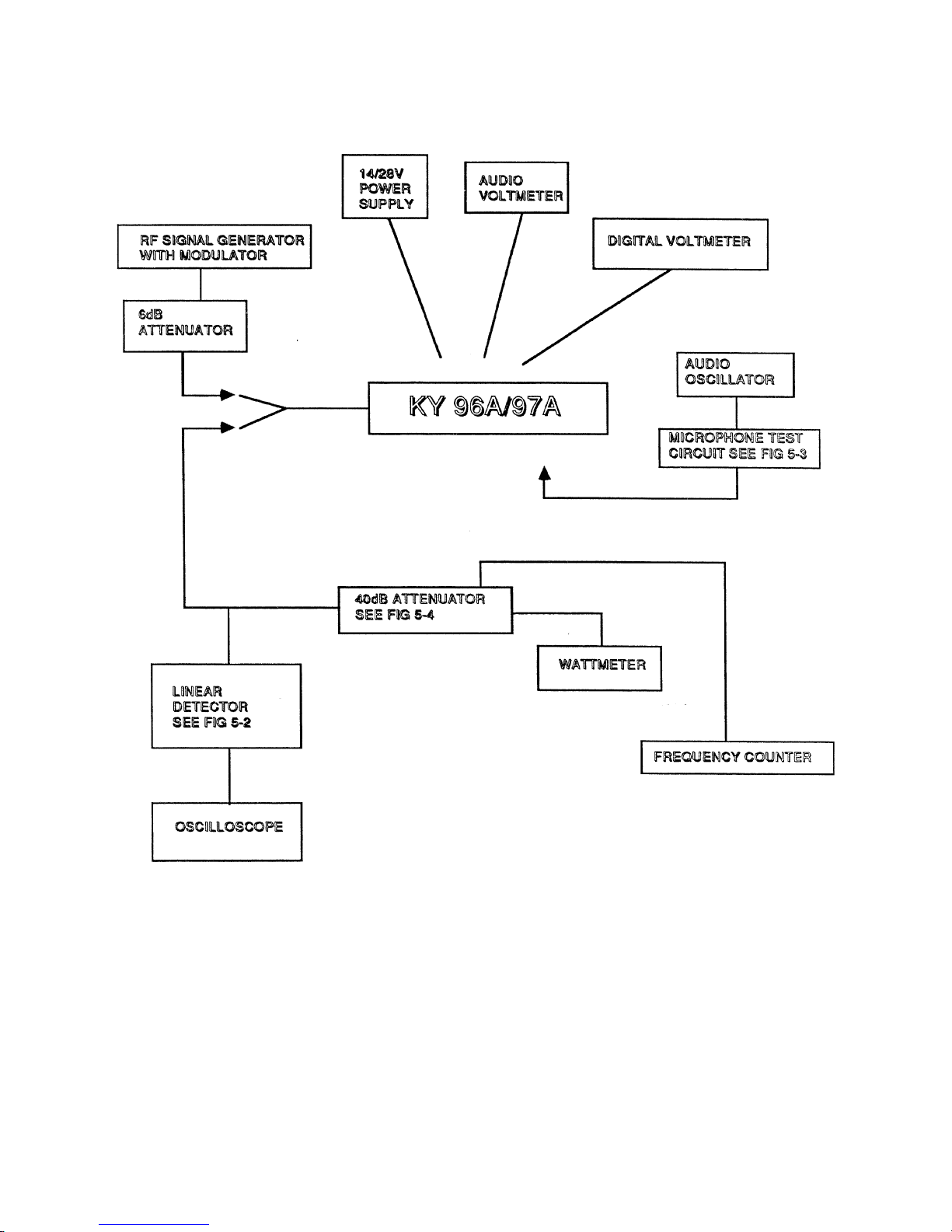
5.2.2 TEST EQUIPMENT SETUP
Connect test equipment according to Figure 5-1.
Rev 5, Apr 2003 MM 006-05674-0005.dwd Page 5-2
Page 26
B KY 96A, KY 97A
FIGURE 5-1 Typical Test Equipment Setup
Rev 5, Apr 2003 MM 006-05674-0005.dwd Page 5-3
Page 27

B KY 96A, KY 97A
5.3 PERFORMANCE TEST PROCEDURE
This section is a cover on return-to-service performance test. The unit shall pass this
performance test after removal of covers, modification, alignment, or repair of the unit
before return to service. The performance test can also be used to locate faults within
the radio.
TEST DATA SHEET Serial No. _________
5.3.1 Control Functions
NOTE: The term “OK” indicates that particular function is operating properly.
5.3.1.A. Display: ___OK viewing angle (straight on).
5.3.1.B. Frequency Controls:
Increment Roll Over Characteristics Decrement Roll Under Characteristics
MHz___OK 135 to 118 MHz MHz___OK 118 to 135 MHz
136 to 118 MHz 118 to 136 MHz
kHz___OK 0.975 to 0.000 kHz kHz___OK 0.000 to 0.975 kHz
5.3.1.C. Transfer Button: ___OK (switches from an active to standby frequency).
5.3.1.D. Remote Transfer: ___OK (switches from an active to standby frequency).
5.3.1.E. Chan Button: ___OK (enters channel mode).
5.3.1.F. Remote Channel Increment: ___OK (increments channel).
5.3.1.G. Program Secure: Channel program secured ___OK.
Channel un-program secured ___OK.
5.3.1.H. Dim Select:
open position ___OK (Display brightness follows 13.75 V lighting bus).
grounded position ___OK (Display brightness follows 27.5 V lighting bus).
aircraft supply position ___OK (Display at half brightness).
5.3.1.I. Memory: ___OK.
When unit is turned “OFF” and then back “ON” that the last display status is
the same.
5.3.1.J. 25 kHz Switch: ___OK
The 25 kHz switch increments in steps of 25 kHz.
5.3.2 Receiver
Rev 5, Apr 2003 MM 006-05674-0005.dwd Page 5-4
Page 28

B KY 96A, KY 97A
NOTE: Disable the audio compressor by grounding pin 10 on P96A1, P97A1.
5.3.2.A. Sensitivity:
5.3.2.A.1 Input a 2 uV standard audio test signal into the unit and monitor receiver audio
while switching modulation off.
S+N/N: 118.000 MHz ______ NLT 6dB
126.975 MHz ______ NLT 6dB
135.975 MHz ______ NLT 6dB
[136.975 MHz] _____ NLT 6dB
5.3.2.A.2 Input a 100 uV standard audio test signal into the unit and monitor receiver
audio while switching modulation off.
Quieting: 126.975 MHz ______NLT 25 dB S+N/N.
5.3.2.B. AGC Characteristics: 126.975 MHz ______ NMT 3 dB
With a standard audio test signal vary from 5 uV to 20,000 uV.
5.3.2.C. Selectivity:
Using the AGC voltage produced by a 3 uV standard signal reference, measure and record the frequencies which reproduce the AGC REF voltage at 6
dB and 60 dB above the reference input.
5.3.2.C.1 6 dB Bandwidth:
126.975 MHz:
Above ___ >
___ >
126.985 MHz Below ___ < 126.965 MHz - 25 kHz units
126.9895 MHz ___ < 126.9605 MHz - 50 kHz units
5.3.2.C.2 60 dB Bandwidth:
126.975 MHz:
Above ___ > 126.995 MHz Below ___ < 126.955 MHz - 25 kHz units
___ >
127.015 MHz ___ < 126.935 MHz - 50 kHz units
5.3.2.D. Volume Gain Control: Min___NMT 22mV Max___NLT 7.07V into 500 ohms
With Audio Amp board installed Max___NLT 4.5V into 500 ohms
Input a 100 uV standard audio test signal into the unit. Disable squelch by
pulling the volume knob out and monitor the audio output.
5.3.2.E. Audio Distortion: (Optional)
350 Hz = ___NMT 15% 1 kHz = ___NMT 15% 2.5 kHz = ___NMT 15%
Input a 100 uV 85% modulated signal between 350 Hz and 2500 Hz. The distortion shall be not more than 15% at 7.07 Vrms into 500 ohms. Modulation
Rev 5, Apr 2003 MM 006-05674-0005.dwd Page 5-5
Page 29

B KY 96A, KY 97A
is referenced to 1 kHz, compressor enabled. (This is an optional test that requires a distortion analyzer).
5.3.2.F. Audio Response:
350 Hz = ___NMT 6dB down 1 kHz = ___ 0dB 2.5 kHz = ___NMT 6dB down
Input a 100 uV standard audio test signal into the unit. Disable the audio compressor by grounding pin 10 on P96A1, P97A1. Monitor the receiver output.
5.3.2.G. Compressor: ______NMT +/- 3 dB
Input a 100 uV standard audio test signal into the unit. Vary the modulation
from 30% to 85%.
5.3.2.H. Squelch:
NOTE: Squelch adjustments must be performed in the following order:
5.3.2.H.1 Set the unit to 126.975 MHz.
5.3.2.H.2 Carrier/Noise Squelch set to open at 2 uV (+1 uV, -0.5 uV) and close at NMT
4 dB below the squelch opening.
5.3.2.H.3 Carrier/Noise Squelch _____OK.
5.3.2.H.4 With unit set to 126.975 MHz, input an 8 kHz 85% modulated signal into the
unit. Set the carrier squelch to open at +/- 12.5 uV.
5.3.2.H.5 Carrier Squelch _____OK.
5.3.2.H.6 Intercom: ______ NLT 100 mW into 500 ohm.
Input a 100 mV 1 kHz signal into Mic Intercom, pin K of P96A1, P97A1.
5.3.3 Transmitter
5.3.3.A. RF Power Output:
Connect a wattmeter to the antenna output and record the following unmodulated values.
Set A + input to ______ 13.75 Vdc @ pin 11______
27.5 Vdc @ pin 12 ______
118.00 MHz ______ 5.0 watts Min. 13.75 V units
126.97 MHz ______ 5.0 watts Min. 13.75 V units
135.97 MHz ______ 5.0 watts Min. 13.75 V units
Rev 5, Apr 2003 MM 006-05674-0005.dwd Page 5-6
______ 5.0 watts Min. 27.5 V units
______ 5.0 watts Min. 27.5 V units
______ 5.0 watts Min. 27.5 V units
Page 30

B KY 96A, KY 97A
After 2 minutes continuous key:
NOTE: Units with Mic-key Disable will shut down transmitter after 2 minutes. To ex-
tend transmit time re-key transmitter.
118.00 MHz ______ 1.25 watts Min. 13.75 V units
______ 1.25 watts Min. 27.5 V units
126.97 MHz ______ 1.25 watts Min. 13.75 V units
______ 1.25 watts Min. 27.5 V units
135.97 MHz ______ 1.25 watts Min. 13.75 V units
______ 1.25 watts Min. 27.5 V units
Low Voltage:
With a low line voltage input the following values should be observed:
22 Vdc for 27.5 V units
11 Vdc for 13.75 V units
118.00 MHz ______ 1.25 watts Min. 13.75 V units
______ 1.25 watts Min. 27.5 V units
126.97 MHz ______ 1.25 watts Min. 13.75 V units
______ 1.25 watts Min. 27.5 V units
135.97 MHz ______ 1.25 watts Min. 13.75 V units
______ 1.25 watts Min. 27.5 V units
5.3.3.B. Modulation Capability:
Input a standard modulator test signal into the microphone audio. Using the
linear detector, measure the Tx modulation.
5.3.3.B.1 118.000 MHz ______ NLT 70%
126.97 MHz ______ NLT 70%
135.97 MHz ______ NLT 70%
5.3.3.B.2 Carrier Noise Level:
Modulate the carrier with 70% at 1000 Hz.
Noise on the carrier with modulation removed shall be NLT:
118.00 MHz ___ 40dB 126.97 MHz ___ 40dB 135.95 MHz ___ 40dB
5.3.3.B.3 Demodulated Audio Distortion (Optional):
350 Hz = ___ 15% Max 1 kHz = ___ 15% Max 2.5 kHz = ___ 15% Max
(This is an optional test that requires a distortion analyzer).
5.3.3.B.4 Sidetone Audio Response:
Rev 5, Apr 2003 MM 006-05674-0005.dwd Page 5-7
Page 31

B KY 96A, KY 97A
350 Hz = ___NMT 6dB down 1 kHz = ___ 0 2.5 kHz = ___NMT 6dB down
Input a standard modulator signal, except voltage is 0.2 Vrms, into Mic Audio.
Monitor the audio output.
5.3.3.B.5 Demodulated Audio Response:
350 Hz = ___NMT 6dB down 1 kHz = ___ 0 2.5 kHz = ___NMT 6dB down
Input a standard modulator signal, except voltage is 0.2 Vrms, into Mic Audio.
Observe the demodulated RF output from the linear detector on an audio wattmeter.
5.3.3.C. Frequency Stability: ______ NMT +/- 200 Hz
Measured after 2 hours “OFF” period.
5.3.4 Audio Amplifier
5.3.4.A. Mute: ______ NLT 40 dB down
With the volume control at minimum and a 1 kHz 4.47 V audio signal applied
to AUX1 audio input when the PTT input is NMT + 0.5 volts.
5.3.4.B. Audio Output Power:
5.3.4.B.1 Comm ______ (4 W min/ 13.75 V unit, 8 W min/ 27.5 V unit)
Insert a 100 uV RF carrier modulated 30% at 1 kHz into the unit. Monitor the
4 ohm audio output.
5.3.4.B.2 Aux1 ______ (4 W min/ 13.75 V unit, 8 W min/ 27.5 V unit)
Insert a 1 kHz 4.47 V (40 mW @ 500 ohms) for 27.5 V units, 3.16 V (20 mW
@ 500 ohms) for 13.75 V units, audio signal into the Aux1 input. With the volume control at minimum, monitor the 4 ohm audio output.
5.3.4.B.3 Aux2 ______ (4 W min/ 13.75 V unit, 8 W min/ 27.5 V unit)
Insert a 1 kHz 4.47 V (40 mW @ 500 ohms) for 27.5 V units, 3.16 V (20 mW
@ 500 ohms) for 13.75 V units, audio signal into the Aux2 input. With the volume control at minimum, monitor the 4 ohm audio output.
5.3.4.B.4 Aux3 ______ (4 W min/ 13.75 V unit, 8 W min/ 27.5 V unit)
Insert a 1 kHz 4.47 V (40 mW @ 500 ohms) for 27.5 V units, 3.16 V (20 mW
@ 500 ohms) for 13.75 V units, audio signal into the Aux3 input. With the volume control at minimum, monitor the 4 ohm audio output.
5.3.4.C. Quieting: S+N/N ______ dB (NLT 25 dB)
Rev 5, Apr 2003 MM 006-05674-0005.dwd Page 5-8
Page 32

B KY 96A, KY 97A
Input a 100 uV standard audio test signal into the unit. Disable the compressor by grounding pin 10 of J97A1, J96A1. Monitor the 4 ohm audio output
while removing modulation.
5.3.4.D. Audio Frequency Response:
5.3.4.D.1 Comm 350 Hz ______ dB
1 kHz ______ dB
2.5 kHz ______ dB
Input a 100 uV standard audio test signal into the unit.
5.3.4.D.2 Aux1 350 Hz ______ dB
1 kHz ______ dB
2.5 kHz ______ dB
Insert a 1 kHz 4.47 V (40 mW @ 500 ohms) audio signal into the Aux1 input.
5.3.4.E. Audio Distortion: (Optional test requiring distortion analyzer)
5.3.4.E.1 Comm 350 Hz ______ % (NMT 15%)
1 kHz ______ % (NMT 15%)
2.5 kHz ______ % (NMT 15%)
5.3.4.E.2 Aux1 350 Hz ______ % (NMT 15%)
1 kHz ______ % (NMT 15%)
2.5 kHz ______ % (NMT 15%)
5.4 ALIGNMENT PROCEDURE
The following procedure is for aligning a KY 96A, KY 97A to meet the minimum performance specifications. If partial alignment is desired, use only the initial control settings that apply to the section being aligned.
5.4.1 Initial Control Settings
R176 Noise Squelch Max CW
R267 Modulation Max CW
R184 RF AGC Max CCW
R221 Sidetone Mid Range
R1009 Mic Gain Mid Range
R801 Volume Control Max CCW (off)
R801 Squelch Test Switch Out (test position)
5.4.2 Voltage Regulator Test
Connect the unit to RF load and apply power. Advance the volume control
R802 (R902) CW to turn on and set to MID-RANGE.
5.4.2.A. Read the voltage at TP103 and adjust R189 for 9 volts +/- 0.1 volt.
5.4.2.B. Read the voltage at TP104 and observe 5.0 volts +/- 0.25 volt.
Rev 5, Apr 2003 MM 006-05674-0005.dwd Page 5-9
Page 33

B KY 96A, KY 97A
5.4.3 VCO Adjust
Set frequency to 135.975 MHz and put unit in transmit mode.
Adjust the Tx frequency to 135.975 MHz using C134. This should be done with-
in 60 seconds of turn on.
Put unit in receive mode. Read voltage at TP102 and adjust T105 for 7.1 volts.
5.4.4 Viewing Angle Adjust
The viewing angle adjust is accessible through an opening on the left side of
the unit front panel. The viewing angle adjust is operator adjustable, and is to
be set for optimum display viewing angle by the operator. No alignment is necessary for unit maintenance or repair.
5.4.5 Transmitter
5.4.5.1 Power Set
Adjust R256 to obtain minimum rated power across the band, unmodulated.
Adjust C418 for minimum power variation across the band.
KY 96A 5 watts
KY 97A 5 watts
5.4.5.2 Modulator Adjust
Set the frequency selector to 128.50 MHz. Apply a 0.4 volt 1 kHz standard test
signal to the microphone input and key the transmitter.
Observe the demodulated RF output from the linear detector on an oscilloscope
and adjust R1009 for 85% modulation.
Adjust R267 for 70% modulation. Check 118.00 MHz and 135.975 MHz and
re-adjust only if the modulation is lower than 70%.
5.4.5.3 Sidetone Adjust
Apply a 0.4 volt 1 kHz standard test signal to the microphone input and key the
transmitter. Adjust R221 for 4 mW of audio into a 500 ohm load.
5.4.6 Receiver Alignment
5.4.6.1 RF/IF Alignment
The following alignment is to be made at 128.50 MHz. Connect the unit to the
RF signal generator through a 6 dB pad. Turn unit on with squelch and compressor disabled and apply sufficient RF signal for approximately 4.75 volts dc
at TP105.
Load and tune L101, L103, L105 and L107 using a 220 ohm resistor from the
top of each tank to ground in the following sequence.
Load L103 tune L101
Load L101 tune L103
Rev 5, Apr 2003 MM 006-05674-0005.dwd Page 5-10
Page 34

B KY 96A, KY 97A
Load L107 tune L105
Load L105 tune L107
Adjust T101, T102, T103, and T104 for maximum ACG voltage. During the
above adjustments, the RF signal should be reduced to keep the AGC voltage
near 4.75 volts.
5.4.6.2 Noise Squelch Adjustments
Apply 2.0 uV (Hard) of RF modulated 30% with 1 kHz and adjust R176 CW until
the receiver just breaks squelch (audio present).
5.4.6.3 Carrier Squelch Adjustments
Apply a 128.50 MHz, 12.5 uV (Hard) signal into the antenna connector modulated 85% at 8 kHz and slowly adjust R184 until squelch just breaks (audio
present).
5.4.6.4 Climax Filter Adjustments
Apply a 128.50 MHz, 100 uV (Hard) signal modulated 85% at 4.5 kHz. Disable
the compressor/ squelch. Monitor the audio output with an audio wattmeter.
Adjust L110 for minimum output (Null).
5.5 OVERHAUL
5.5.1 Visual Inspection
The following visual inspection procedures should be performed during the course of
maintenance operations.
5.5.1.1 Inspect all wiring for frayed, loose, cracked, or burned wires.
5.5.1.2 Check that cable connections are free of corrosion and are properly secured.
5.5.1.3 Check all components for evidence of overheating, breakage, vibration, corrosion, or loose connections.
5.5.1.4 Check all capacitors and transformers for leaks, bulges, or loose connections.
5.5.1.5 Inspect relay and switch contacts for pits or arcing.
5.5.2 Cleaning
5.5.2.1 Use a clean, lint-free cloth, lightly moistened with an approved cleaning agent
to remove foreign matter from the unit case and front panel. Wipe dry with a
clean, dry, lint-free cloth.
5.5.2.2 Use a hand controlled dry air jet (not more than 15 psi) to blow the dust from
inaccessible areas.
Rev 5, Apr 2003 MM 006-05674-0005.dwd Page 5-11
Page 35

B KY 96A, KY 97A
5.5.2.3 Clean electrical contacts with a burnishing tool or cloth lightly moistened with
an approved contact cleaner.
5.5.2.4 Clean the receptacles and plugs with a hand controlled dry air jet (not more
than 25 psi) and a clean, lint-free cloth, lightly moistened with an approved
cleaning agent. Wipe dry with a clean, dry, lint-free cloth.
Rev 5, Apr 2003 MM 006-05674-0005.dwd Page 5-12
Page 36
B KY 96A, KY 97A
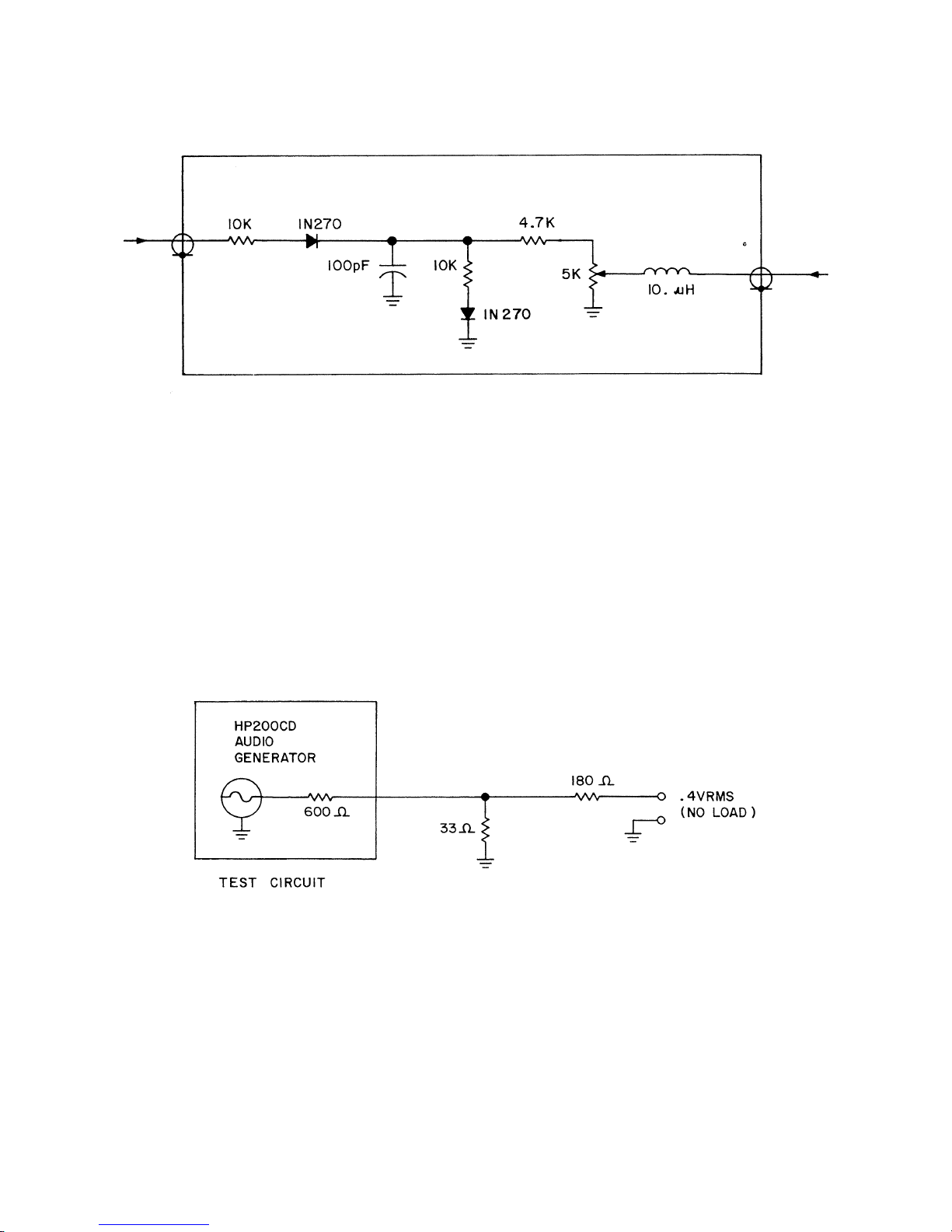
FIGURE 5-2 Linear Detector
Rev 5, Apr 2003 MM 006-05674-0005.dwd Page 5-13
FIGURE 5-3 Mic Test Circuit
Page 37
B KY 96A, KY 97A
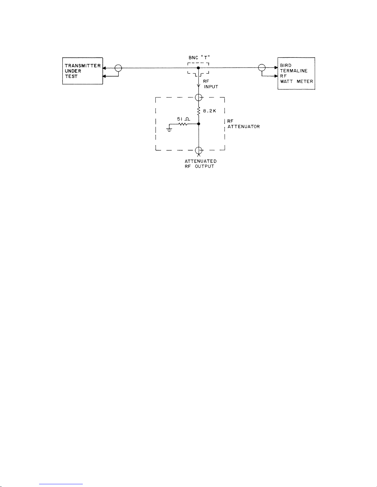
FIGURE 5-4 40 dB Attenuator
Rev 5, Apr 2003 MM 006-05674-0005.dwd Page 5-14
Page 38
B KY 96A, KY 97A
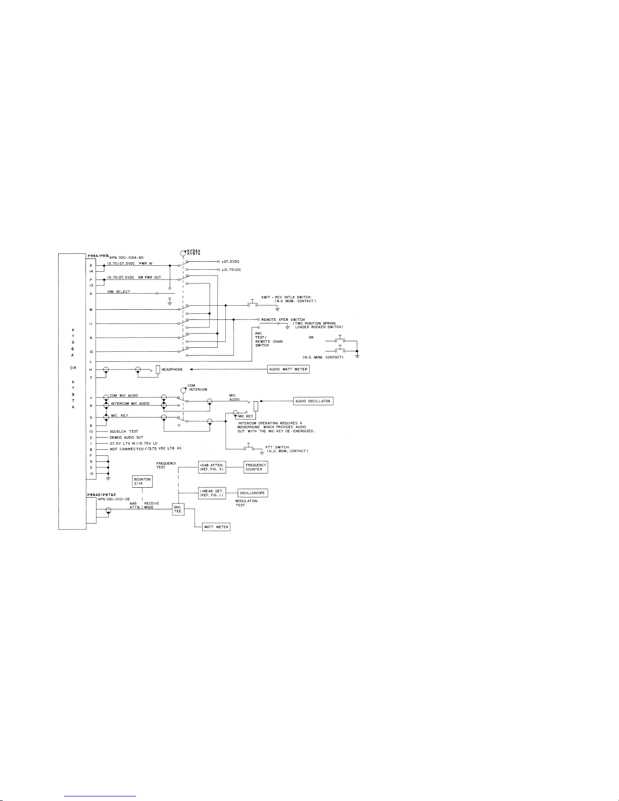
Rev 5, Apr 2003 MM 006-05674-0005.dwd Page 5-15
FIGURE 5-5 Bench Test Harness
Page 39
B KY 96A, KY 97A
SECTION VI
ILLUSTRATED PARTS LIST
6.1 INTRODUCTION
The Illustrated Parts List (IPL) contains parts lists of assemblies and discrete components required for the unit. The IPL provides the proper identification and part number of each replacement part. The IPL starts with the top assembly and continues in sequence with the sub-assembly parts lists. Mechanical parts are grouped separately from electrical parts on each subassembly parts list. Each parts list is followed by the assembly drawing for that assembly.
Parts lists may also be called “bills of material” or “BOM.” Parts identified in this IPL meet design specifications for this equipment and are recommended replacement parts. Warranty information concerning replacement parts is contained in Service Memo #1, P/N 600-0800100XX.
6.2 BILL OF MATERIAL DESCRIPTION
This section describes the various items that may appear on parts lists. Refer to figure 6-0 for
the parts list format.
1000
6.2.1 PARTS LIST (ASSEMBLY) NUMBER
Each parts list is labeled with the assembly part number at the top of the list. The assembly
number is followed by the assembly description and the revision level of the parts list.
6.2.2 SYMBOL COLUMN
The symbol column contains the reference designators of electrical components on the assembly. Some mechanical parts and assembly supplies may be assigned the ITM designator.
Reference documents may be assigned the REF designator. The reference designator contains a letter abbreviation to indicate the type of component, and the sequence number assigned to that part (C101, Q101, etc.). Common reference designator abbreviations are listed
in Table 6-1.
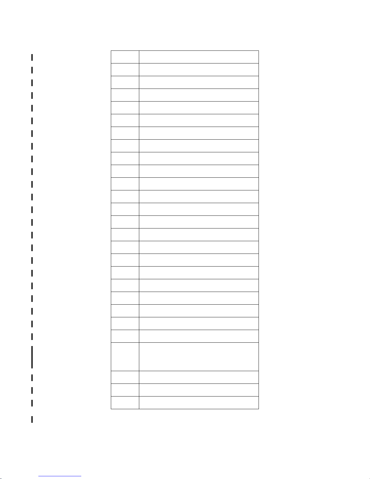
Table 6-1: Reference Designator Abbreviations
B Motor, Synchro
C Capacitor
CF Capacitor Filter
CJ Circuit Jumper
CQ Capacitor
CR Diode
D Diode
DS Lamp
E Terminal, Connect Point
F Fuse
Rev 5, Apr 2003 MM 006-05674-0005.dwd Page 6-1
Page 40
B KY 96A, KY 97A
Table 6-1: Reference Designator Abbreviations
FB Ferrite Bead
FL Filter
FT Feedthru
I Integrated Circuit
ITM Item (Non-electrical)
J Jack, Fixed Connector
KRelay
L Inductor
M Meter, Transistor
MX Mixer
P Plug, Removable Connector
Q Transistor
RResistor
REF Reference Document
RP Resistor Network
RT Thermistor
RV Varistor
S Switch
SK Socket
SW Switch
T Transformer
TJ Terminal Jack
TP Test Point
U Integrated Circuit, Circuit Assembly,
Component Network (Resistor,
Capacitor, Inductor, Transistor, Diode)
V Photocell, Vacuum Tube, Varistor
WG Waveguide
Y Crystal
Rev 5, Apr 2003 MM 006-05674-0005.dwd Page 6-2
Page 41

B KY 96A, KY 97A
6.2.3 PART NUMBER COLUMN
The part number column contains the Honeywell part number for each part. Special purpose
part number series may appear in the parts list and are described below.
6.2.3.1 U401 122-XXXXX-9999 PLACE HOLDER
Circuit U401 is a programmed device with a -9999 place holder. Its true part number is contained on the next higher 125- P/N or 126- P/N software configuration. Refer to Section 6.3,
Software Documentation, in this introduction, for a description of the software documentation
system.
6.2.3.2 U402 999-09999-0090 REF SFTWARE SET
Circuit U402 is a programmed device. Its true part number is contained on the next higher
125- P/N or 126- P/N software configuration. Refer to Section 6.3, Software Documentation,
in this introduction, for a description of the software documentation system.
6.2.3.3 CR401 999-09999-0096 RESERVED
Reference designator CR401 has been reserved for future use. The assembly does not currently include a CR401.
6.2.3.4 CR401 999-09999-0097 SEE NEXT ASSEMBLY
Diode CR401 is a part of the electrical circuit, but due to assembly or testing requirements, is
actually assigned to the next assembly.
6.2.3.5 CR401 999-09999-0098 NOT USED
Reference designator CR401 is available for future assignment. The assembly does not currently include a CR401.
6.2.3.6 CR401 999-09999-0099 DO NOT USE
Reference designator CR401 has been previously used on this assembly and later deleted. It
may not be reassigned on this assembly.
6.2.4 FIND_NO COLUMN
This column lists the find (item) number of a part. Find numbers of mechanical parts may appear on the assembly drawing. Find numbers of electrical parts do not appear on the assembly drawing. Find numbers are not assigned to every part and missing information in this column is not an error.
6.2.5 DESCRIPTION COLUMN
This column describes each part in the assembly. Common abbreviations in the description
column are listed in Table 6-2.
Table 6-2: Description Abbreviations
A Ampere
ADC Analog to Digital Converter
ADJ Adjustable
AL, ALUM Aluminum
Rev 5, Apr 2003 MM 006-05674-0005.dwd Page 6-3
Page 42
B KY 96A, KY 97A
Table 6-2: Description Abbreviations
AMP Ampere, Amplifier
ANT Antenna
ASSY Assembly
BD Board
BI Two
BIFLR Bifilar
BLK Black
BLU Blue
BOM Bill of Material (= Parts List)
BRN Brown
CA Cable
CC Carbon Composite
CF Carbon Film
CH Chip, Choke
CAP Capacitor
CER, CR Ceramic
CKT Circuit
CNTCT Contact
CONN Connector
CVR Cover
DAC Digital to Analog Converter
DBL Double
DC Disc Ceramic
DIO Diode
DPDT Double Pole Double Throw
DPST Double Pole Single Throw
DUAL, DUO Two
DWG Drawing
EL Electrolytic
EW Eighth Watt
Rev 5, Apr 2003 MM 006-05674-0005.dwd Page 6-4
Page 43
B KY 96A, KY 97A
Table 6-2: Description Abbreviations
FC Fixed Composition
FERR Ferrite
FET Field Effect Transistor
FHP Flat Head Phillips
FLTR Filter
FREQ Frequency
FT Feedthru
GHZ Gigahertz
GND Ground
GRN Green
GRY Gray
HDR Header
HDW Hardware
HEX Six
HF High Frequency
HV High Voltage
HW Half Watt
H/W Hardware
IC Integrated Circuit
ID, IDT Identification
IF Intermediate Frequency
IND Inductor
INTER Interconnect
INTL Internal
I/O In/Out
ITM Item
KHZ Kilohertz
LCK, LK Lock
LED Light Emitting Diode
LSI Large Scale Integrated Circuit
Rev 5, Apr 2003 MM 006-05674-0005.dwd Page 6-5
Page 44
B KY 96A, KY 97A
Table 6-2: Description Abbreviations
MA Milliamp
MC Monolithic Ceramic
MF Microfarad
MH Millihenry
MHZ Megahertz
MOD Modification
MOS Metal Oxide Semiconductor
MPS Minimum Performance Specification
MY Mylar
NF Nanofarad
NPN Negative-Positive-Negative transistor type
OCTAL Eight
OP AMP Operational Amplifier
ORG, ORN Orange
OSC Oscillator
PA Power Amplifier
PC Polycarbonate, Printed Circuit
PCB, PCBD Printed Circuit Board
PENTA Five
PF Precision Film, Picofarad
PHP Pan Head Phillips
PKG Package
P/L Parts List
PLD Programmable Logic Device
PLL Phase-Locked Loop
PLT Plate
P/N Part Number
PNP Positive-Negative-Positive transistor type
POS Positive, Position
PP Paper
Rev 5, Apr 2003 MM 006-05674-0005.dwd Page 6-6
Page 45
B KY 96A, KY 97A
Table 6-2: Description Abbreviations
PRGA Programmable Gate Array
PROM Programmable Read Only Memory
PS Polystyrene, Power Supply
PWR Power
QUAD Four
QW Quarter Watt
RAM Random Access Memory
RCVR Receiver
RECPT Receptacle
REF Reference
REG Regulator
RES Resistor
RF Radio Frequency
ROM Read Only Memory
RX Receive, Receiver
S Silicon
SCH Schematic
SCR Screw
SFTWR Software
SM Silver Mica, Surface Mount
SMD Surface Mount Device
SMT Surface Mount Technology
S/N Serial Number
SO, SOT Small Outline
SPDT Single Pole Double Throw
SPST Single Pole Single Throw
SRAM Synchronous Random Access Memory
STDF Standoff
SW Switch
S/W Software
Rev 5, Apr 2003 MM 006-05674-0005.dwd Page 6-7
Page 46
B KY 96A, KY 97A
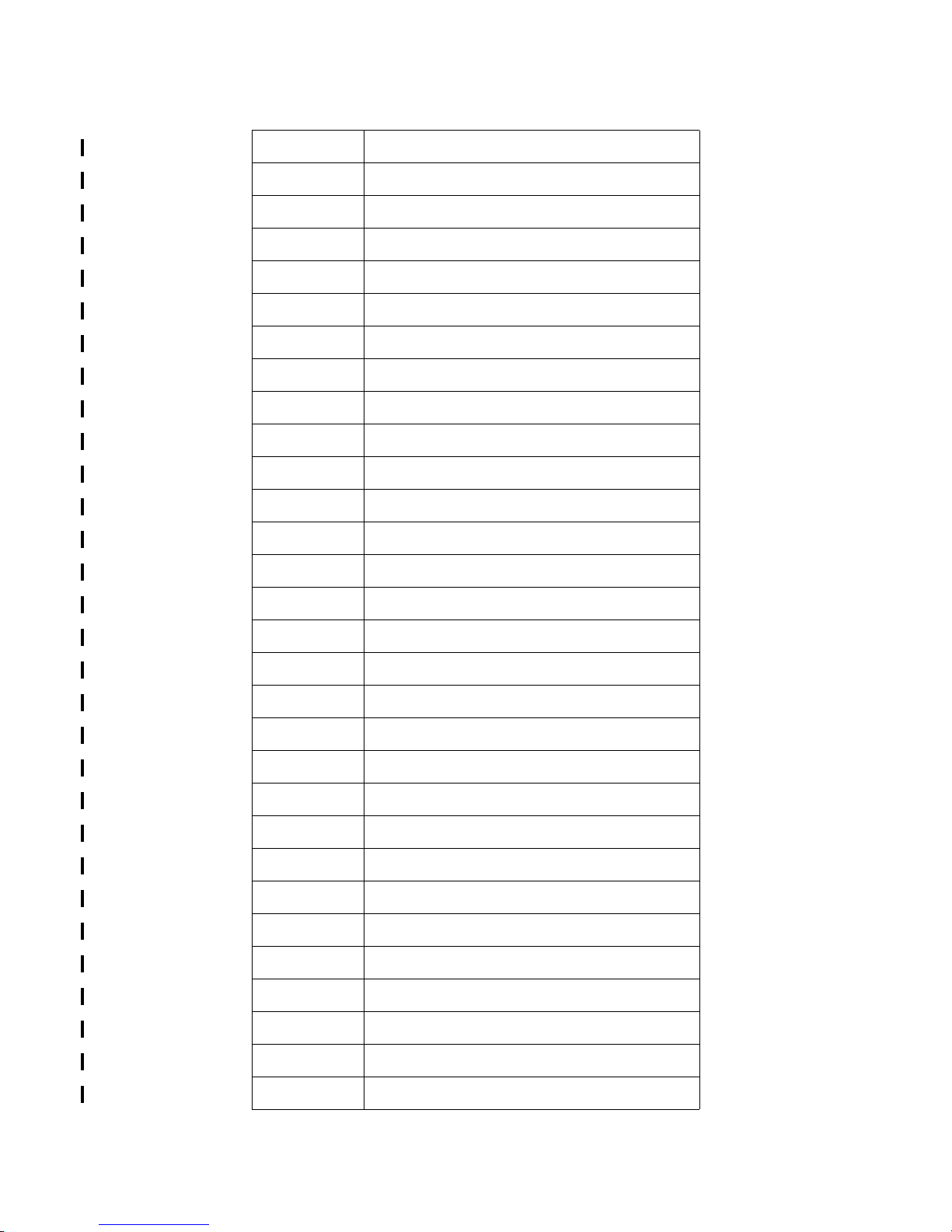
Table 6-2: Description Abbreviations
SYN Synthesizer
SYNC Synchronizer
SYS System
TCXO Temperature Controlled Crystal Oscillator
TERM Terminal
TN Tantalum
TP Test Point
TRI Three
TRML Terminal
TRNSB Transorber
TST PT Test Point
TURR Turret
TW Tenth Watt
TX Transmit, Transmitter
U Integrated Circuit
UA Microamp
UF Microfarad
UH Microhenry
UHF Ultra High Frequency
UP Microprocessor
VVolt
VA, VAR Variable
VCO Voltage Controlled Oscillator
VIO Violet
VHF Very High Frequency
VLT Voltage
WWatt
W/ With, Width
WHT White
WW Wire Wound
Rev 5, Apr 2003 MM 006-05674-0005.dwd Page 6-8
Page 47
B KY 96A, KY 97A
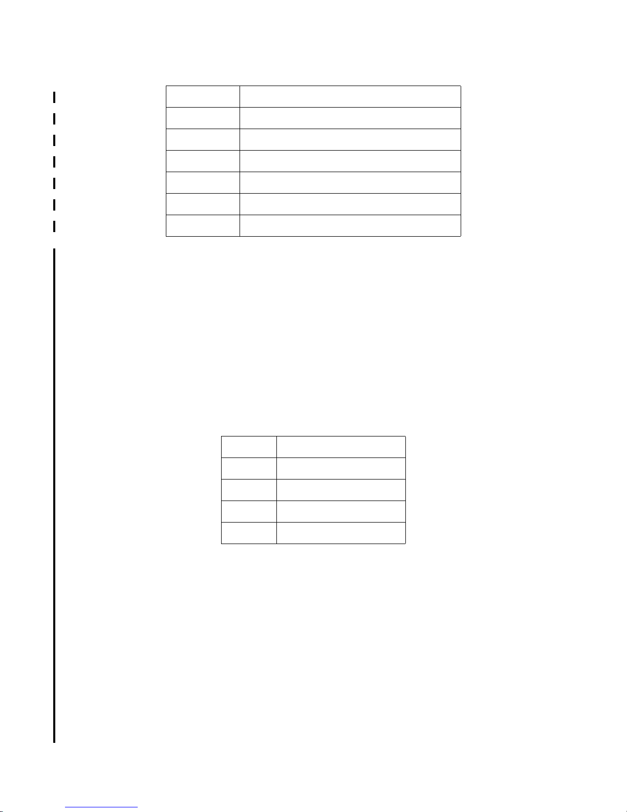
Table 6-2: Description Abbreviations
WX Weather
XFMR Transformer
XMIT Transmit, Transmitter
XSTR Transistor
XTAL Crystal
YEL Yellow
Z Zener
6.2.6 ASSEMBLY (A) COLUMN
An “A” in this column indicates that the part is a sub-assembly. Each sub-assembly has a separate parts lists following the parent assembly. If the sub-assembly is a “COMMON BOM” with
a -9900, -0099, or -9999 suffix, the parts for that common assembly are included in the parent
assembly parts list as a separate column.
6.2.7 UNIT OF MEASURE (UM) COLUMN
This column indicates the unit of measure for each part. Common abbreviations found in this
column are listed in Table 6-3.
Table 6-3:
6.2.8 VERSION AND QUANTITY COLUMN
Individual versions of an assembly are identified by the last four digits of the P/N. The quantity
of parts for individual versions are listed in separate version columns -0000 through -9999.
The parts indicated in -0099, -9900, or -9999 version columns are common to all versions of
the assembly and constitute the “COMMON BOM.” Versions may also be called “flavors” in
parts lists. The terms are interchangeable.
Unit of Measure Abbreviations
AR As Required
EA Each
FT Foot
IN Inch
RF Reference Only
6.3 SOFTWARE DOCUMENTATION
Unit software configuration is documented through several dedicated part number series. If a
unit contains software, the 206-XXXXX-XXXX P/N series designates the overall unit software/
hardware configuration set. The 205-XXXXX-XXXX P/N series designates the software/hardware circuit board sets. The 126-XXXXX-XXXX P/N series designates non-software programmable device sets. The 125-XXXXX-XXXX P/N series designates software programmable de-
Rev 5, Apr 2003 MM 006-05674-0005.dwd Page 6-9
Page 48
B KY 96A, KY 97A
vice sets. The 122-XXXXX-XXXX P/N series designates discrete programmed devices within
the 126- P/N and 125- P/N device sets.
The top unit parts list contains the 206- P/N unit software/hardware configuration set. In some
cases, specific versions of 206- P/N unit SW/HW configuration sets must be used in specific
versions of unit part numbers. An example of a 206- P/N unit SW/HW configuration set is
shown in figure 6-0, sheet 1, item “A” in the right hand margin.
The last two or four digits of software related P/N's indicate the revision number (-XXRN) of
the software. Those numbers are incremented with each revision of software.
If a circuit board contains software, the applicable 205- P/N is used to order the programmed
software/hardware board set. A board with software cannot be ordered by hardware 200- or
300- P/Ns. The applicable 122- P/N is used to order programmed devices. In some cases,
specific versions of programmed devices must be used with specific versions of other programmed devices in the unit. Programmed devices cannot be ordered by 125- or 126- P/Ns.
6.3.1 UNIT SOFTWARE/HARDWARE SYSTEM SET
The 206- P/N is the configuration control for all unit software, software/hardware circuit boards,
and programmed devices in the unit. The 206- P/N parts list contains the software identification tag and any 205- P/N software/hardware board sets. The last two or last four digits of the
206- P/N designate the software/hardware configuration version of the unit, depending on
whether the unit part number is 9-digit or 12-digit.
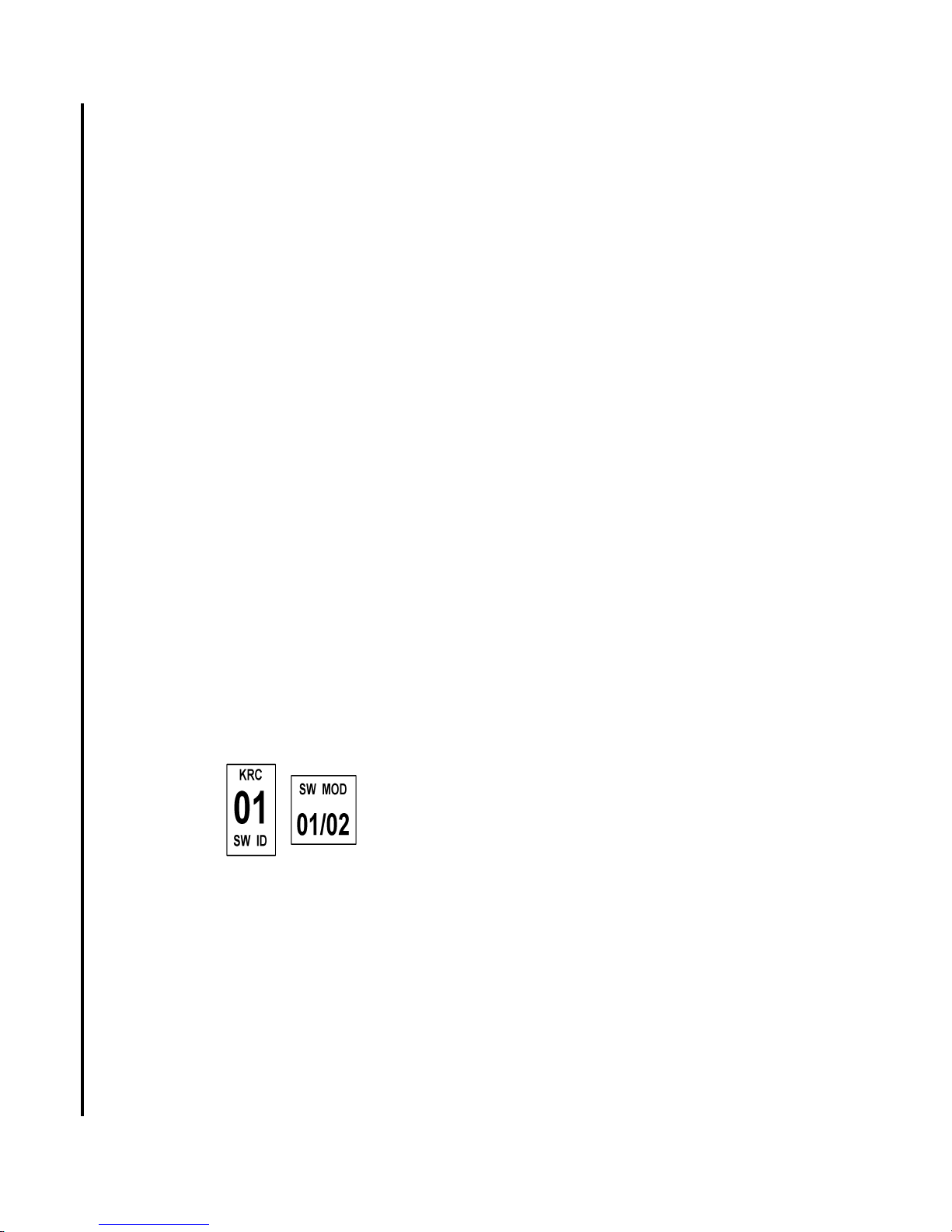
6.3.1.1 When the unit part number is 9-digits on the TSO label, the last 2 digits of the 206- P/N
are the last two digits of the software identification tag attached to the unit. The SW identification tag part number is 057-03284-00XX, where XX is the last two digits of the 206- P/N.
6.3.1.2 When the unit part number is 12-digits on the TSO label, the last 4 digits of the 206- P/
N are the last 4 digits of the software identification tag attached to the unit. The SW identification tag part number is 057-05287-YYYY, where YYYY is the last four digits of the 206- P/
N. The two types of software identification tags are illustrated below.
6.3.1.3 The 205- P/N software/hardware board sets used in the unit appear on the 206- P/N soft-
ware/hardware configuration set parts list. An example of a 205- P/N software/hardware board
set is shown in figure 6-0, sheet 1, item “B” in the right hand margin.
6.3.2 SOFTWARE/HARDWARE BOARD SETS
The 205- P/N series designates software/hardware board set assemblies. The 205- P/N parts
list contains 057- P/N SW/HW board labels, and contains 125- P/N software programmable
device sets and/or 126- P/N non-software programmable device sets that fulfill software requirements. The 125- P/N and 126- P/N device sets contain 122- P/N programmed devices.
The 205- P/N parts list also contains the 200- P/N or 300- P/N hardware circuit board.
6.3.2.1 The 057- P/N SW/HW board labels:
Rev 5, Apr 2003 MM 006-05674-0005.dwd Page 6-10
Page 49

B KY 96A, KY 97A
6.3.2.1.1 For 9-digit 205-WWWW-RN board labels, the first 7 digits are contained on a label part
number 057-050WW-00WW, and the last two digits are specified by 057-05252-00RN. The
revision number (RN) of the 205-WWWW-RN and the 057-05252-00RN part numbers are incremented when the revision number of any 125-0XXXX-XXRN part number is incremented.
Therefore, the revision number of the 205-WWWW-RN and 057-05252-00RN part numbers
will be the same.
6.3.2.1.2 For 12-digit 205-0XXXX-XXRN board labels, the first 10 digits are contained on a label
part number 057-05252-XXXX, and the last two digits are specified by 057-05335-00RN. The
revision number (RN) of the 205-0XXXX-XXRN and the 057-05335-00RN part numbers are
incremented when the revision number of any 125-0XXXX-XXRN part number is incremented.
Therefore, the revision number of the 205-0XXXX-XXRN and 057-05335-00RN part numbers
will be the same. A circuit board identification tag is illustrated below.
205-06616-
6.3.2.2 The 125- software programmable device sets:
The 205- P/N SW/HW board set may contain one or more 125- P/N software programmable
device sets. A 125- P/N software programmable device set contains software and one or more
122- P/N programmed devices designated for that software function. When the revision number (RN) of any one of the 122-0XXXX-XXRN programmed devices is incremented in a new
software release, the revision number the 125-0XXXX-XXRN device set is also incremented.
This 125- P/N parts list also specifies the “U” or “I” circuit designators for the programmed devices found on assembly drawings and schematic diagrams. Examples of 125- P/N sets are
shown in figure 6-0, sheet 1, items “C1,” and “C2” in the right hand margin.
6.3.2.3 The 126- P/N non-software programmable device sets:
When specified at the 205- P/N SW/HW board set level, the 126- P/N non-software programmable device set fulfills software requirements. The 126- P/N parts list contains one or more
122-0YYYY-YYRN P/N programmed devices. An example of a 126- P/N set that fulfills software requirements is shown in figure 6-0, sheet 1, item “C3” in the right hand margin.
6.3.2.4 The 122- P/N programmed devices:
The 122-0XXXX-XXRN part number identifies discrete programmed devices found in both
software programmable 125- P/N device sets and non-software programmable 126- P/N device sets that perform a software function. These parts also appear on the 200- P/N or 300P/N hardware board parts list as 122-0XXXX-9999. Their true part number is found only on
the 125- P/N or 126- P/N parts list.
0000
6.3.2.5 The 200- P/N or 300-P/N hardware board:
The 200- P/N or 300- P/N hardware circuit board is specified by the 205- SW/HW board set.
An example of a 200- P/N hardware board reference on a 205- SW/HW board set is shown in
figure 6-0, sheet 1, last line.
6.3.3 HARDWARE BOARDS WITH PROGRAMMED DEVICES
The 200- P/N or 300- P/N hardware board parts list contains 126- P/N non-software programmable device sets that fulfill hardware requirements and reference to all 122- P/N programmed
devices on the hardware board.
6.3.3.1 The 126- P/N non-software programmable device sets:
Rev 5, Apr 2003 MM 006-05674-0005.dwd Page 6-11
Page 50

B KY 96A, KY 97A
The 126- P/N non-software programmable device sets that fulfill hardware requirements appear on the 200- P/N or 300- P/N parts list.
6.3.3.2 The 122- P/N programmed devices:
The 122- P/N programmed devices appear on the 200- P/N or 300- P/N parts list. These references resolve device location on the board. Component designators are placed in the SYMBOL field of the parts list to specify component location. These include 122-3XXXX-9999 or
122-0YYYY-9999 part numbers.
The 122- numbers in the form 122-3XXXX-9999 are used for non-software programmable devices (126- P/N) that fulfill hardware requirements. Examples of such 122- P/Ns are shown in
figure 6-0, sheet 2, items “D5” through “D10” in the right hand margin.
The 122- numbers of the form 122-0YYYY-9999 are used for both software programmable devices (125-) (Items D12 through D15, in the example), and non-software programmable devices (126-) (Item D11, in the example), that fulfill software requirements.
These programmable device sets appear on the hardware/software board (205-) parts list.
The exact programmable device (the resolution of the -9999, in the above items) is specified
by the respective software programmable device set (125-), or the non-software programmable device set (126-) parts list.
Using the SYMBOL field as specified above, would discourage the use of the SYMBOL field
for this purpose, in the programmable device sets (125- and 126-) parts list. This would then
permit the specification of the same programmable device sets in different boards, hence different component designators. In the example, Figure 6-0:
• The items flagged D1 through D4, in the right margin, are non-software programmable
device sets.
• The items flagged D5 through D10, in the right margin, are non-software programmable device designators, that fulfill hardware requirements.
• The item flagged D11, in the right margin, is a non-software programmable device designator, that fulfills software requirements.
• The items flagged D12 through D15, in the right margin, are software programmable
device designators, that fulfill software requirements.
Figure 6-0, while closely related to a specific product, does not represent an exact configuration in use by that product. The example has been modified to clarify certain points.
Rev 5, Apr 2003 MM 006-05674-0005.dwd Page 6-12
Page 51
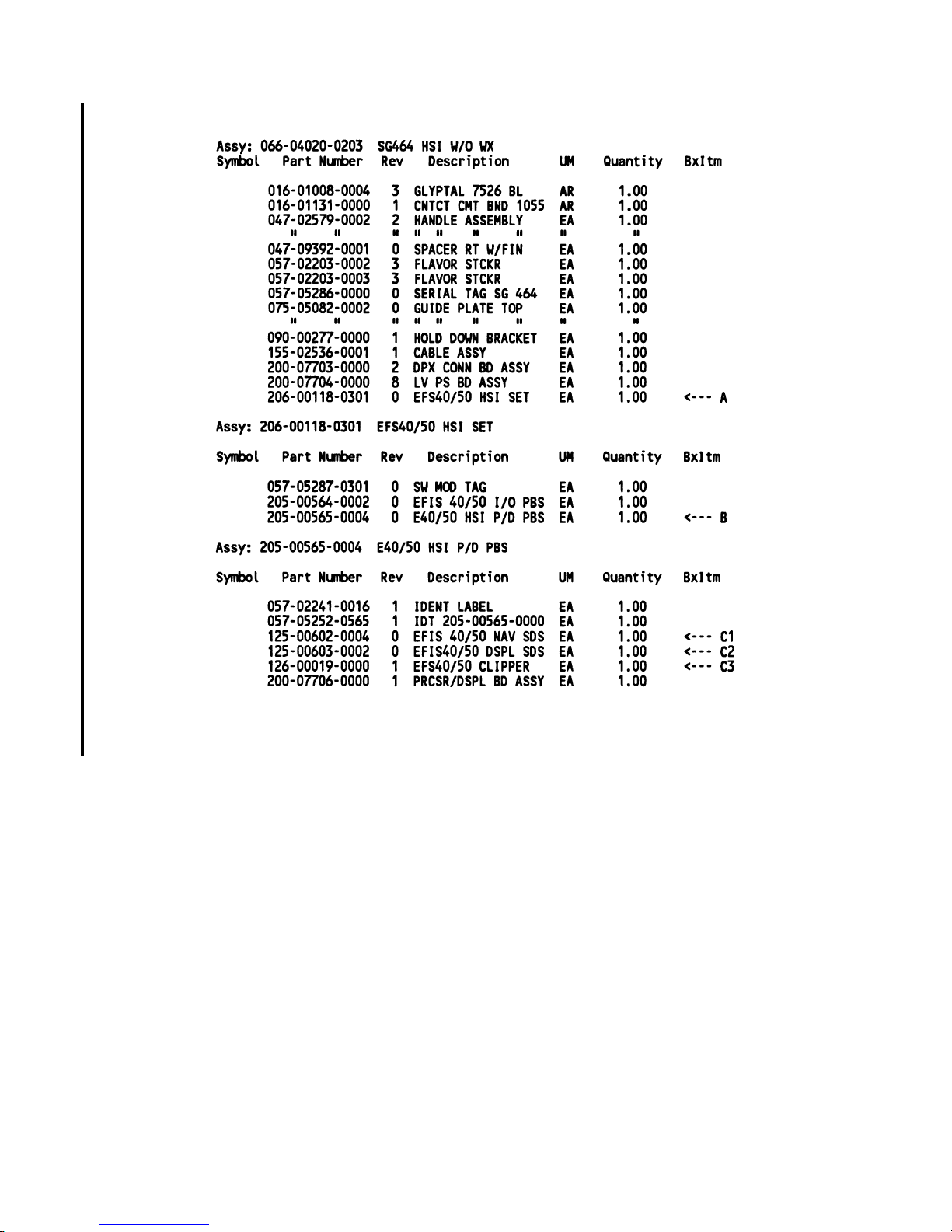
B KY 96A, KY 97A
Figure 6-0 Sample Parts List
(Sheet 1 of 4)
Rev 5, Apr 2003 MM 006-05674-0005.dwd Page 6-13
Page 52
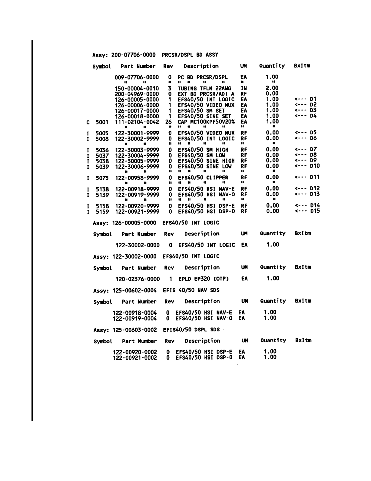
B KY 96A, KY 97A
Rev 5, Apr 2003 MM 006-05674-0005.dwd Page 6-14
Figure 6-0 Sample Parts List
(Sheet 2 of 4)
Page 53
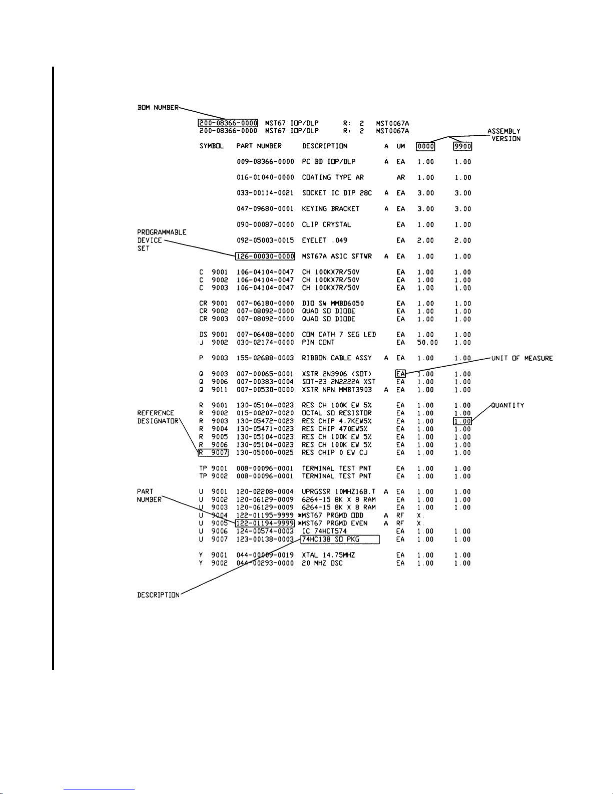
B KY 96A, KY 97A
Rev 5, Apr 2003 MM 006-05674-0005.dwd Page 6-15
Figure 6-0 Sample Parts List
(Sheet 3 of 4)
Page 54
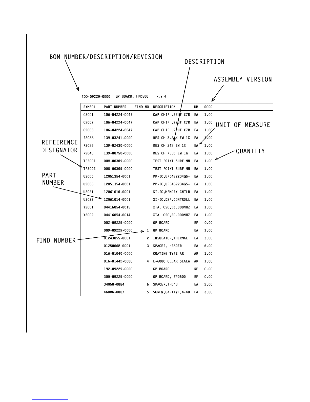
B KY 96A, KY 97A
Rev 5, Apr 2003 MM 006-05674-0005.dwd Page 6-16
Figure 6-0 Sample Parts List
(Sheet 4 of 4)
Page 55

B KY 96A, KY 97A
6.4 ILLUSTRATED PARTS LIST
6.4.1 KY 96A VHF Communication Transceiver
064-01052-0010 96A 25KHZ SEL REV AB
064-01052-0011 96A 50KHZ SEL REV AB
064-01052-0030 96A 25K SEL 136975 REV AB
064-01052-0099 COMMOM BOM REV AD
-----------------------------------------------------------------------------------SYMBOL PART NUMBER FIND NO DESCRIPTION UM -0010 -0011 -0030 -0099
-----------------------------------------------------------------------------------I108 120-03026-0000 IC MC7805CT EA . . . 1.00
Q113 007-00930-0000 XSTR S PNPMJE15029 EA . . . 1.00
Q122 007-00930-0000 XSTR S PNPMJE15029 EA . . . 1.00
REF1 300-04268-0000 KY96A COMM TRANSC RF . . . .00
REF100 000-00601-0002 PRODUCT STRUCTURE RF . . . .00
012-01005-0002 TAPE MYLAR .500 W IN . . . .50
012-01127-0000 TAG COVER EA . . . 4.00
013-00006-0001 FERR BEAD EA . . . 4.00
016-01008-0004 GLYPTAL 7526 BL AR . . . 1.00
016-01015-0000 IND ADH 3M 4475 AR . . . 1.00
016-01071-0000 DC RTV 3140 AR . . . 1.00
025-00005-0002 WIRE 18 RED IN . . . 10.75
025-00005-0012 WIRE 18 RD/WH IN . . . 9.00
025-00018-0022 WIRE 26 RED IN . . . 2.00
025-00018-0024 WIRE 26 RD/YL IN . . . 11.00
025-00018-0092 WIRE 26 WH/RD IN . . . 10.50
025-00018-0096 WIRE 26 WH/BU IN . . . 10.50
025-05012-0000 WIRE 2C SHD WHTBLK IN . . . 9.50
030-02229-0011 RGT ANG HDR 3P EA . . . 1.00
030-02229-0013 RGT ANG HDR 7P EA . . . 1.00
030-02229-0014 RGT ANG HDR 6P EA . . . 1.00
035-01007-0020 CONN CVR NAS820-8 EA . . . 1.00
035-01361-0020 PROTECTIVE COVER EA . . . 1.00
047-04811-0001 COVER XMTR W/F EA . . . 1.00
047-08494-0501 TOP COVER ASSEMBLY EA 1.00 1.00 1.00 .
047-08495-0002 COVER, BOTTOM EA . . . 1.00
047-08512-0004 MOUNTING RACK EA . . . 1.00
057-01540-0000 WARNING HV TAG EA . . . 1.00
057-02203-1010 S/N TAG FLVR BLK EA 1.00 . . .
057-02203-1011 S/N TAG FLVR BLK EA . 1.00 . .
057-02203-1030 S/N TAG FLVR BLK EA . . 1.00 .
057-02312-0001 DECAL EA . 1.00 . .
057-02337-0000 PRTCTV CVR DECAL EA . . . 1.00
057-03451-0001 S/N TAG KY96A EA . . . 1.00
057-03511-0001 DECAL, CAUTION EA . . . 1.00
064-01052-0099 COMMOM BOM EA 1.00 1.00 1.00 .
073-00808-0003 KNOB VOLUME EA . . . 1.00
088-00838-0006 PUSH BUTTON EA . . . 1.00
088-02269-0003 BEZEL LCD EA . . . 1.00
088-02270-0000 PUSH BUTTON, RND EA . . . 1.00
088-02271-0000 LIGHTING SHAFT EA . . . 1.00
089-05434-0003 SCR FHP 3-48X3/16 EA . . . 9.00
089-05434-0004 SCR FHP 3-48X1/4 EA . . . 8.00
089-05874-0005 SCR PHP 2-56X5/16 EA . . . 1.00
089-05899-0003 SCR PHP 2-56X3/16 EA . . . 1.00
089-05901-0004 SCR PHP 3-48X1/4 EA . . . 7.00
089-05903-0004 SCR PHP 4-40X1/4 EA . . . 3.00
089-05925-0004 SCR BHP 3-48X1/4 EA . . . 5.00
089-06298-0004 SCR FHP 3-48X1/4 EA . . . 2.00
089-06342-0004 SCR PHP 3-48X1/4 EA . . . 4.00
090-00991-0000 PROTECTIVE CLOSURE EA . . . 1.00
091-00109-0000 CABLE TIE EA . . . 2.00
Rev 5, Apr 2003 MM 006-05674-0005.dwd Page 6-17
Page 56

B KY 96A, KY 97A
-----------------------------------------------------------------------------------SYMBOL PART NUMBER FIND NO DESCRIPTION UM -0010 -0011 -0030 -0099
----------------------------------------------------------------------------------- 091-00156-0000 BUSHING EA . . . 3.00
091-00286-0002 INSUL XSTR .687 EA . . . 2.00
150-00049-0010 SHRINK TUBING WHT IN . . . 1.25
150-00060-0001 SPIROBAND IN . . . 5.25
150-00072-0004 SLDR SLEEVE .62 EA . . . 2.00
150-00103-0000 SLDR SLEEVE EA . . . 2.00
200-04271-0000 28V MODULATOR ASSY EA . . . 1.00
200-07479-0000 LCD DISPLAY BD EA . . . 1.00
200-07540-0001 KY 96A 28V 5W TX B EA . . . 1.00
200-07799-0021 96A MN BD 25K FUJI EA 1.00 . 1.00 .
200-07799-0023 96A MN BD 50K FUJI EA . 1.00 . .
206-00021-0020 TOP SW BOM, KY96A/ EA 1.00 1.00 . .
206-00022-0020 TOP SW BOM, KY96A/ EA . . 1.00 .
Rev 5, Apr 2003 MM 006-05674-0005.dwd Page 6-18
Page 57

B KY 96A, KY 97A
064-01052-0031 96A 50K SEL 136975 REV AB
064-01052-0050 96A 25KHZ W/AUDAMP REV AB
064-01052-0051 96A 50KHZ W/AUDAMP REV AB
064-01052-0099 COMMOM BOM REV AD
-----------------------------------------------------------------------------------SYMBOL PART NUMBER FIND NO DESCRIPTION UM -0031 -0050 -0051 -0099
-----------------------------------------------------------------------------------I108 120-03026-0000 IC MC7805CT EA . . . 1.00
Q113 007-00930-0000 XSTR S PNPMJE15029 EA . . . 1.00
Q122 007-00930-0000 XSTR S PNPMJE15029 EA . . . 1.00
REF1 300-04268-0000 KY96A COMM TRANSC RF . . . .00
REF100 000-00601-0002 PRODUCT STRUCTURE RF . . . .00
012-01005-0002 TAPE MYLAR .500 W IN . . . .50
012-01127-0000 TAG COVER EA . . . 4.00
013-00006-0001 FERR BEAD EA . . . 4.00
016-01008-0004 GLYPTAL 7526 BL AR . . . 1.00
016-01015-0000 IND ADH 3M 4475 AR . . . 1.00
016-01071-0000 DC RTV 3140 AR . . . 1.00
025-00005-0002 WIRE 18 RED IN . . . 10.75
025-00005-0012 WIRE 18 RD/WH IN . . . 9.00
025-00018-0022 WIRE 26 RED IN . . . 2.00
025-00018-0024 WIRE 26 RD/YL IN . . . 11.00
025-00018-0092 WIRE 26 WH/RD IN . . . 10.50
025-00018-0096 WIRE 26 WH/BU IN . . . 10.50
025-05012-0000 WIRE 2C SHD WHTBLK IN . . . 9.50
030-02229-0011 RGT ANG HDR 3P EA . . . 1.00
030-02229-0013 RGT ANG HDR 7P EA . . . 1.00
030-02229-0014 RGT ANG HDR 6P EA . . . 1.00
035-01007-0020 CONN CVR NAS820-8 EA . . . 1.00
035-01361-0020 PROTECTIVE COVER EA . . . 1.00
047-04811-0001 COVER XMTR W/F EA . . . 1.00
047-08494-0501 TOP COVER ASSEMBLY EA 1.00 . . .
047-08495-0002 COVER, BOTTOM EA . . . 1.00
047-08512-0004 MOUNTING RACK EA . . . 1.00
047-12516-0501 TOP COVER ASSY EA . 1.00 1.00 .
057-01540-0000 WARNING HV TAG EA . . . 1.00
057-02203-1031 S/N TAG FLVR BLK EA 1.00 . . .
057-02203-1050 S/N TAG FLVR BLK EA . 1.00 . .
057-02203-1051 S/N TAG FLVR BLK EA . . 1.00 .
057-02312-0001 DECAL EA 1.00 . 1.00 .
057-02337-0000 PRTCTV CVR DECAL EA . . . 1.00
057-03451-0001 S/N TAG KY96A EA . . . 1.00
057-03511-0001 DECAL, CAUTION EA . . . 1.00
064-01052-0099 COMMOM BOM EA 1.00 1.00 1.00 .
073-00808-0003 KNOB VOLUME EA . . . 1.00
088-00838-0006 PUSH BUTTON EA . . . 1.00
088-02269-0003 BEZEL LCD EA . . . 1.00
088-02270-0000 PUSH BUTTON, RND EA . . . 1.00
088-02271-0000 LIGHTING SHAFT EA . . . 1.00
089-05434-0003 SCR FHP 3-48X3/16 EA . . . 9.00
089-05434-0004 SCR FHP 3-48X1/4 EA . . . 8.00
089-05874-0005 SCR PHP 2-56X5/16 EA . . . 1.00
089-05899-0003 SCR PHP 2-56X3/16 EA . . . 1.00
089-05901-0004 SCR PHP 3-48X1/4 EA . . . 7.00
089-05903-0004 SCR PHP 4-40X1/4 EA . . . 3.00
089-05925-0004 SCR BHP 3-48X1/4 EA . . . 5.00
089-06004-0003 SCR FHP 2-56X3/16 EA . 5.00 5.00 .
089-06298-0004 SCR FHP 3-48X1/4 EA . . . 2.00
089-06342-0004 SCR PHP 3-48X1/4 EA . . . 4.00
090-00991-0000 PROTECTIVE CLOSURE EA . . . 1.00
091-00109-0000 CABLE TIE EA . . . 2.00
091-00156-0000 BUSHING EA . . . 3.00
091-00286-0002 INSUL XSTR .687 EA . . . 2.00
150-00049-0010 SHRINK TUBING WHT IN . . . 1.25
150-00060-0001 SPIROBAND IN . . . 5.25
150-00072-0004 SLDR SLEEVE .62 EA . . . 2.00
Rev 5, Apr 2003 MM 006-05674-0005.dwd Page 6-19
Page 58

B KY 96A, KY 97A
-----------------------------------------------------------------------------------SYMBOL PART NUMBER FIND NO DESCRIPTION UM -0031 -0050 -0051 -0099
----------------------------------------------------------------------------------- 150-00103-0000 SLDR SLEEVE EA . . . 2.00
200-04271-0000 28V MODULATOR ASSY EA . . . 1.00
200-07475-0000 LCD PROCESSOR BD EA . 1.00 . .
200-07479-0000 LCD DISPLAY BD EA . . . 1.00
200-07540-0001 KY 96A 28V 5W TX B EA . . . 1.00
200-07797-0000 AUDIO AMP BOARD EA . 1.00 1.00 .
200-07799-0021 96A MN BD 25K FUJI EA . 1.00 . .
200-07799-0023 96A MN BD 50K FUJI EA 1.00 . 1.00 .
206-00021-0020 TOP SW BOM, KY96A/ EA . 1.00 1.00 .
206-00022-0020 TOP SW BOM, KY96A/ EA 1.00 . . .
Rev 5, Apr 2003 MM 006-05674-0005.dwd Page 6-20
Page 59

B KY 96A, KY 97A
064-01052-0060 96A 25KHZ36975W/AM REV AB
064-01052-0061 96A50KHZ36975W/AMP REV AB
064-01052-0070 KY96A FINAL ASSY REV AF
064-01052-0099 COMMOM BOM REV AD
-----------------------------------------------------------------------------------SYMBOL PART NUMBER FIND NO DESCRIPTION UM -0060 -0061 -0070 -0099
-----------------------------------------------------------------------------------I108 120-03026-0000 IC MC7805CT EA . . 1.00 1.00
Q113 007-00930-0000 XSTR S PNPMJE15029 EA . . 1.00 1.00
Q122 007-00930-0000 XSTR S PNPMJE15029 EA . . 1.00 1.00
REF1 300-04268-0000 KY96A COMM TRANSC RF . . .00 .00
REF100 000-00601-0002 PRODUCT STRUCTURE RF . . .00 .00
012-01005-0002 TAPE MYLAR .500 W IN . . .50 .50
012-01127-0000 TAG COVER EA . . 4.00 4.00
013-00006-0001 FERR BEAD EA . . 4.00 4.00
016-01008-0004 GLYPTAL 7526 BL AR . . 1.00 1.00
016-01015-0000 IND ADH 3M 4475 AR . . 1.00 1.00
016-01071-0000 DC RTV 3140 AR . . 1.00 1.00
025-00005-0002 WIRE 18 RED IN . . 11.25 10.75
025-00005-0012 WIRE 18 RD/WH IN . . 9.00 9.00
025-00018-0022 WIRE 26 RED IN . . 2.00 2.00
025-00018-0024 WIRE 26 RD/YL IN . . 11.00 11.00
025-00018-0092 WIRE 26 WH/RD IN . . 10.50 10.50
025-00018-0096 WIRE 26 WH/BU IN . . 10.50 10.50
025-05012-0000 WIRE 2C SHD WHTBLK IN . . 9.50 9.50
030-02229-0011 RGT ANG HDR 3P EA . . 1.00 1.00
030-02229-0013 RGT ANG HDR 7P EA . . 1.00 1.00
030-02229-0014 RGT ANG HDR 6P EA . . 1.00 1.00
035-01007-0020 CONN CVR NAS820-8 EA . . 1.00 1.00
035-01361-0020 PROTECTIVE COVER EA . . 1.00 1.00
047-04811-0001 COVER XMTR W/F EA . . 1.00 1.00
047-08495-0002 COVER, BOTTOM EA . . 1.00 1.00
047-08512-0004 MOUNTING RACK EA . . 1.00 1.00
047-12516-0501 TOP COVER ASSY EA 1.00 1.00 1.00 .
057-01540-0000 WARNING HV TAG EA . . 1.00 1.00
057-02203-1060 S/N TAG FLVR BLK EA 1.00 . . .
057-02203-1061 S/N TAG FLVR BLK EA . 1.00 . .
057-02203-1070 S/N TAG FLVR BLK EA . . 1.00 .
057-02312-0001 DECAL EA . 1.00 . .
057-02337-0000 PRTCTV CVR DECAL EA . . 1.00 1.00
057-03451-0001 S/N TAG KY96A EA . . 1.00 1.00
057-03511-0001 DECAL, CAUTION EA . . 1.00 1.00
064-01052-0099 COMMOM BOM EA 1.00 1.00 . .
073-00808-0003 KNOB VOLUME EA . . . 1.00
073-00972-0003 KNOB VOLUME EA . . 1.00 .
088-00838-0006 PUSH BUTTON EA . . . 1.00
088-00838-0050 LIGHTING SHAFT EA . . 1.00 .
088-02269-0003 BEZEL LCD EA . . . 1.00
088-02270-0000 PUSH BUTTON, RND EA . . . 1.00
088-02270-0001 PUSH BUTTON EA . . 1.00 .
088-02271-0000 LIGHTING SHAFT EA . . 1.00 1.00
088-03101-0007 BEZEL COMPL KY96A EA . . 1.00 .
088-03130-0001 TRANSFER BUTTON EA . . 1.00 .
089-05434-0003 SCR FHP 3-48X3/16 EA . . 9.00 9.00
089-05434-0004 SCR FHP 3-48X1/4 EA . . 8.00 8.00
089-05874-0005 SCR PHP 2-56X5/16 EA . . 1.00 1.00
089-05899-0003 SCR PHP 2-56X3/16 EA . . 1.00 1.00
089-05901-0004 SCR PHP 3-48X1/4 EA . . 7.00 7.00
089-05903-0004 SCR PHP 4-40X1/4 EA . . 3.00 3.00
089-05925-0004 SCR BHP 3-48X1/4 EA . . 5.00 5.00
089-06004-0003 SCR FHP 2-56X3/16 EA 5.00 5.00 5.00 .
089-06298-0004 SCR FHP 3-48X1/4 EA . . 2.00 2.00
089-06342-0004 SCR PHP 3-48X1/4 EA . . 4.00 4.00
090-00991-0000 PROTECTIVE CLOSURE EA . . 1.00 1.00
091-00109-0000 CABLE TIE EA . . 2.00 2.00
091-00156-0000 BUSHING EA . . 3.00 3.00
Rev 5, Apr 2003 MM 006-05674-0005.dwd Page 6-21
Page 60

B KY 96A, KY 97A
-----------------------------------------------------------------------------------SYMBOL PART NUMBER FIND NO DESCRIPTION UM -0060 -0061 -0070 -0099
----------------------------------------------------------------------------------- 091-00286-0002 INSUL XSTR .687 EA . . 2.00 2.00
150-00049-0010 SHRINK TUBING WHT IN . . 1.25 1.25
150-00060-0001 SPIROBAND IN . . 5.25 5.25
150-00072-0004 SLDR SLEEVE .62 EA . . 2.00 2.00
150-00103-0000 SLDR SLEEVE EA . . 2.00 2.00
200-04271-0000 28V MODULATOR ASSY EA . . 1.00 1.00
200-07479-0000 LCD DISPLAY BD EA . . . 1.00
200-07479-0001 LCD DISPLAY BD EA . . 1.00 .
200-07540-0001 KY 96A 28V 5W TX B EA . . 1.00 1.00
200-07797-0000 AUDIO AMP BOARD EA 1.00 1.00 1.00 .
200-07799-0021 96A MN BD 25K FUJI EA 1.00 . 1.00 .
200-07799-0023 96A MN BD 50K FUJI EA . 1.00 . .
206-00022-0020 TOP SW BOM, KY96A/ EA 1.00 1.00 1.00 .
Rev 5, Apr 2003 MM 006-05674-0005.dwd Page 6-22
Page 61
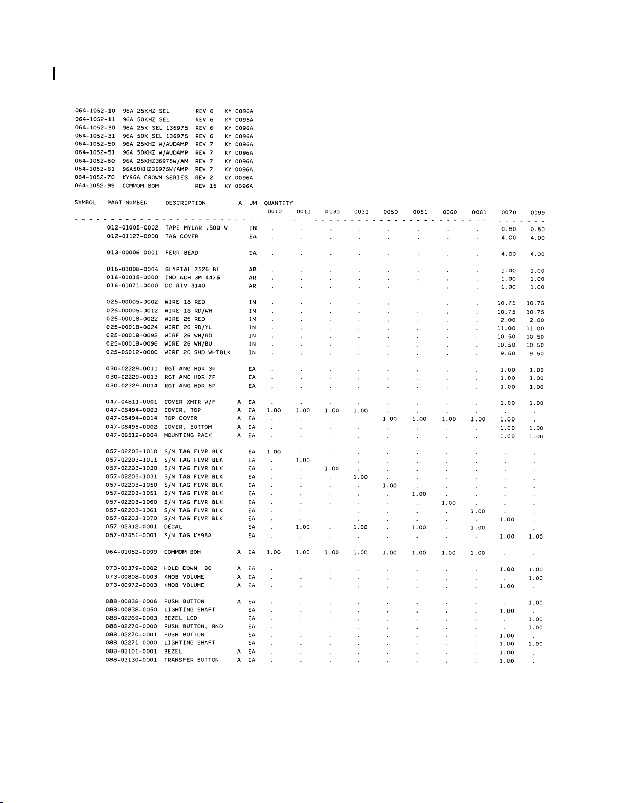
B KY 96A, KY 97A
THIS PAGE CONTAINS OLD REVISION BOMS, FOR REFERENCE ONLY.
Rev 5, Apr 2003 MM 006-05674-0005.dwd Page 6-23
Page 62
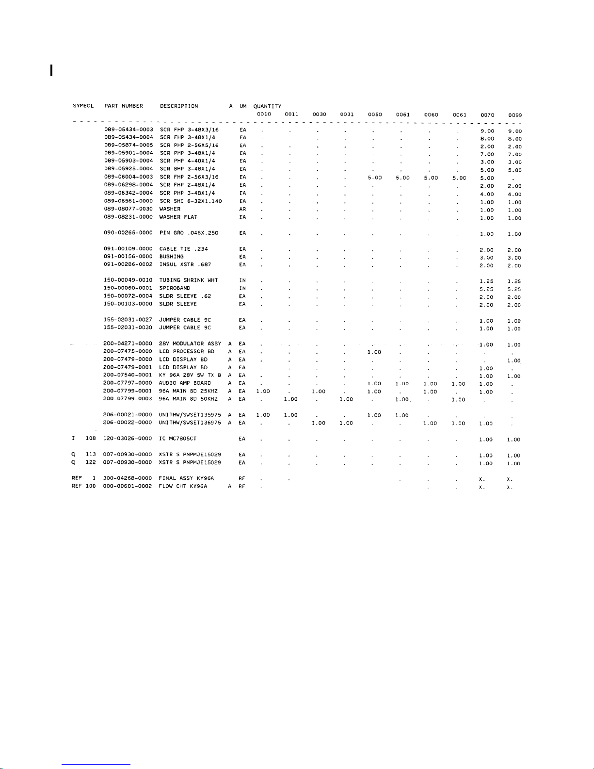
B KY 96A, KY 97A
THIS PAGE CONTAINS OLD REVISION BOMS, FOR REFERENCE ONLY.
Rev 5, Apr 2003 MM 006-05674-0005.dwd Page 6-24
Page 63
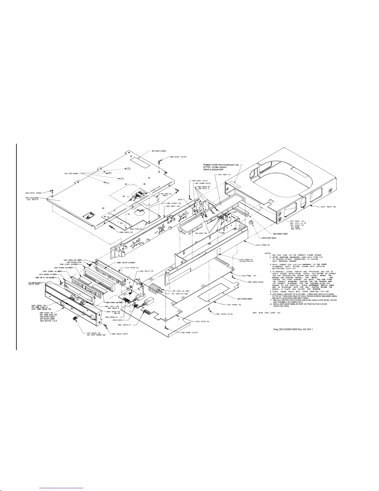
B KY 96A, KY 97A
Rev 5, Apr 2003 MM 006-05674-0005.dwd Page 6-25
FIGURE 6-1 KY 96A Final Assembly (Sht 1 of 2)
(Dwg No 300-04268-0000, Rev AG, Sht 1)
Page 64
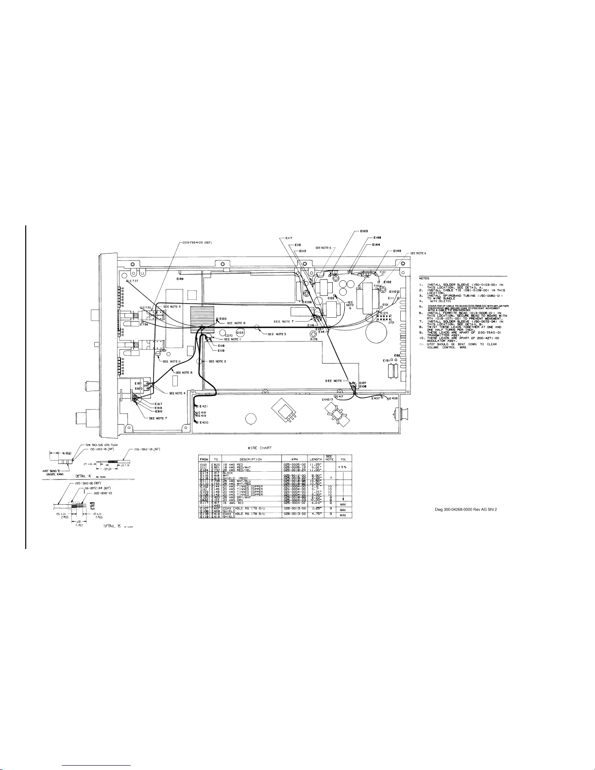
B KY 96A, KY 97A
Rev 5, Apr 2003 MM 006-05674-0005.dwd Page 6-27
FIGURE 6-1 KY 96A Final Assembly (Sht 2 of 2)
(Dwg No 300-04268-0000, Rev AG, Sht 2)
Page 65
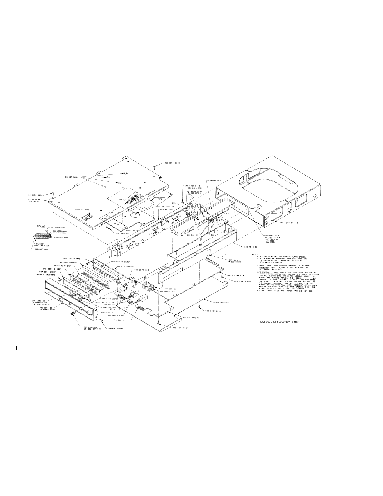
B KY 96A, KY 97A
Rev 5, Apr 2003 MM 006-05674-0005.dwd Page 6-29
FIGURE 6-1A KY 96A Final Assembly (Sht 1 of 2)
(Dwg No 300-04268-0000, Rev 12, Sht 1)
Page 66
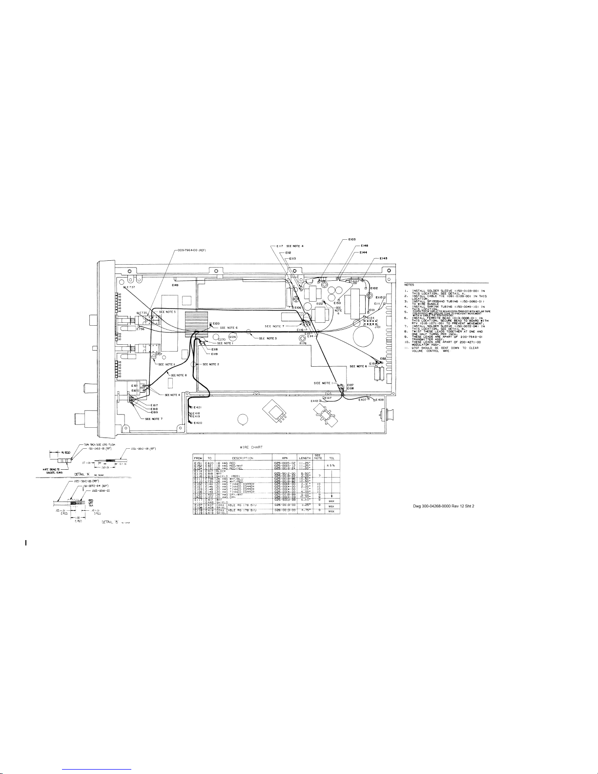
B KY 96A, KY 97A
Rev 5, Apr 2003 MM 006-05674-0005.dwd Page 6-31
FIGURE 6-1A KY 96A Final Assembly (Sht 2 of 2)
(Dwg No 300-04268-0000, Rev 12, Sht 2)
Page 67
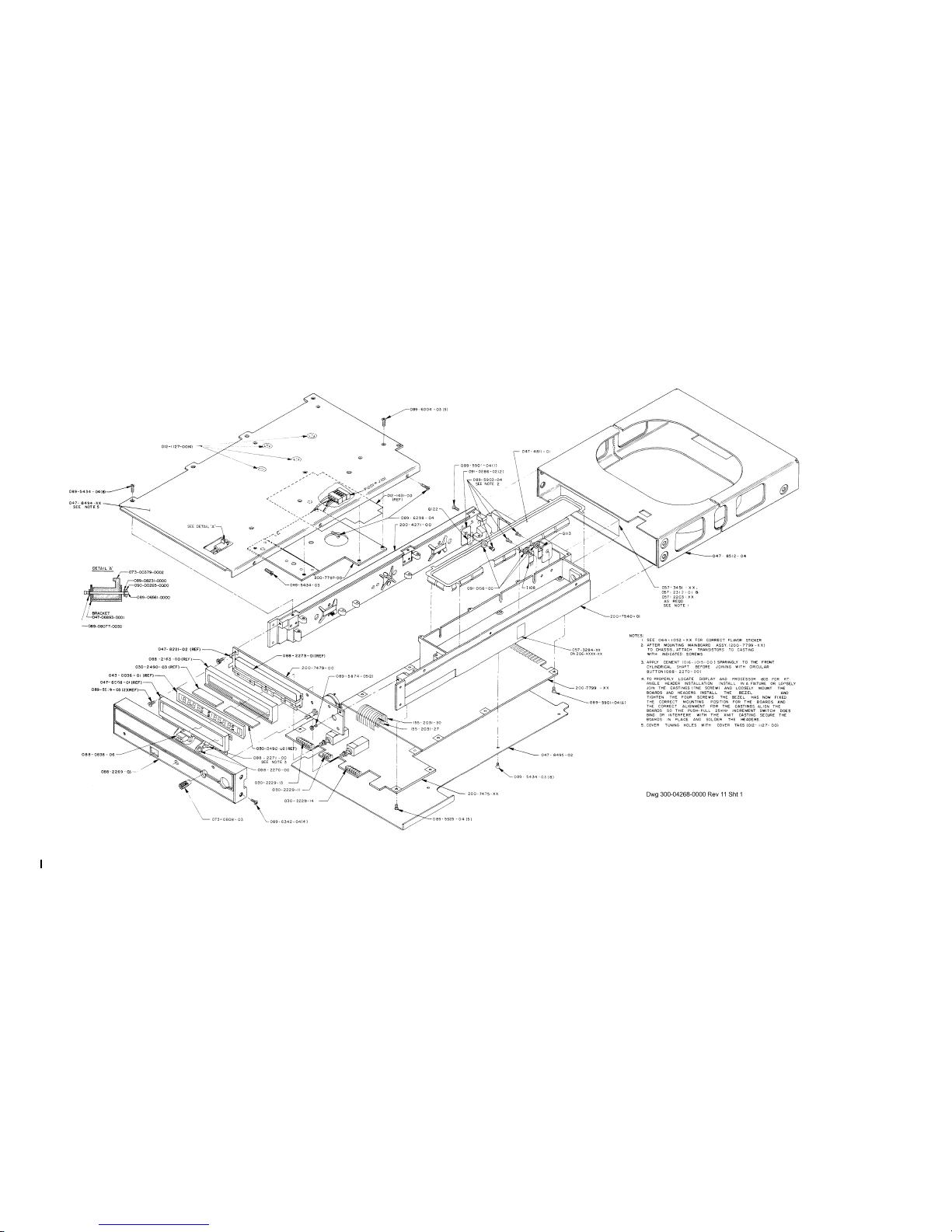
B KY 96A, KY 97A
Rev 5, Apr 2003 MM 006-05674-0005.dwd Page 6-33
FIGURE 6-1B KY 96A Final Assembly (Sht 1 of 2)
(Dwg No 300-04268-0000, Rev 11, Sht 1)
Page 68
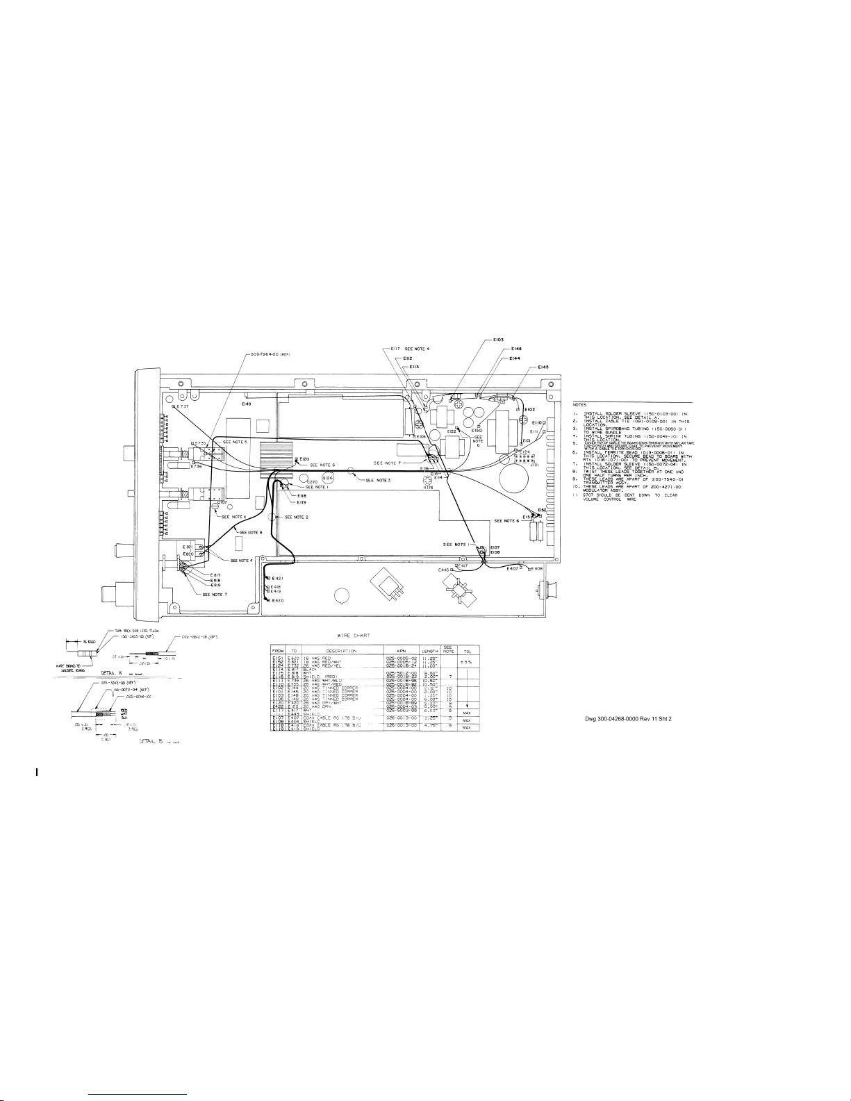
B KY 96A, KY 97A
Rev 5, Apr 2003 MM 006-05674-0005.dwd Page 6-35
FIGURE 6-1B KY 96A Final Assembly (Sht 2 of 2)
(Dwg No 300-04268-0000, Rev 11, Sht 2)
Page 69
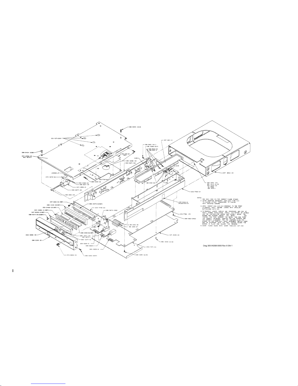
B KY 96A, KY 97A
Rev 5, Apr 2003 MM 006-05674-0005.dwd Page 6-37
FIGURE 6-1C KY 96A Final Assembly (Sht 1 of 2)
(Dwg No 300-04268-0000, Rev 8, Sht 1)
Page 70
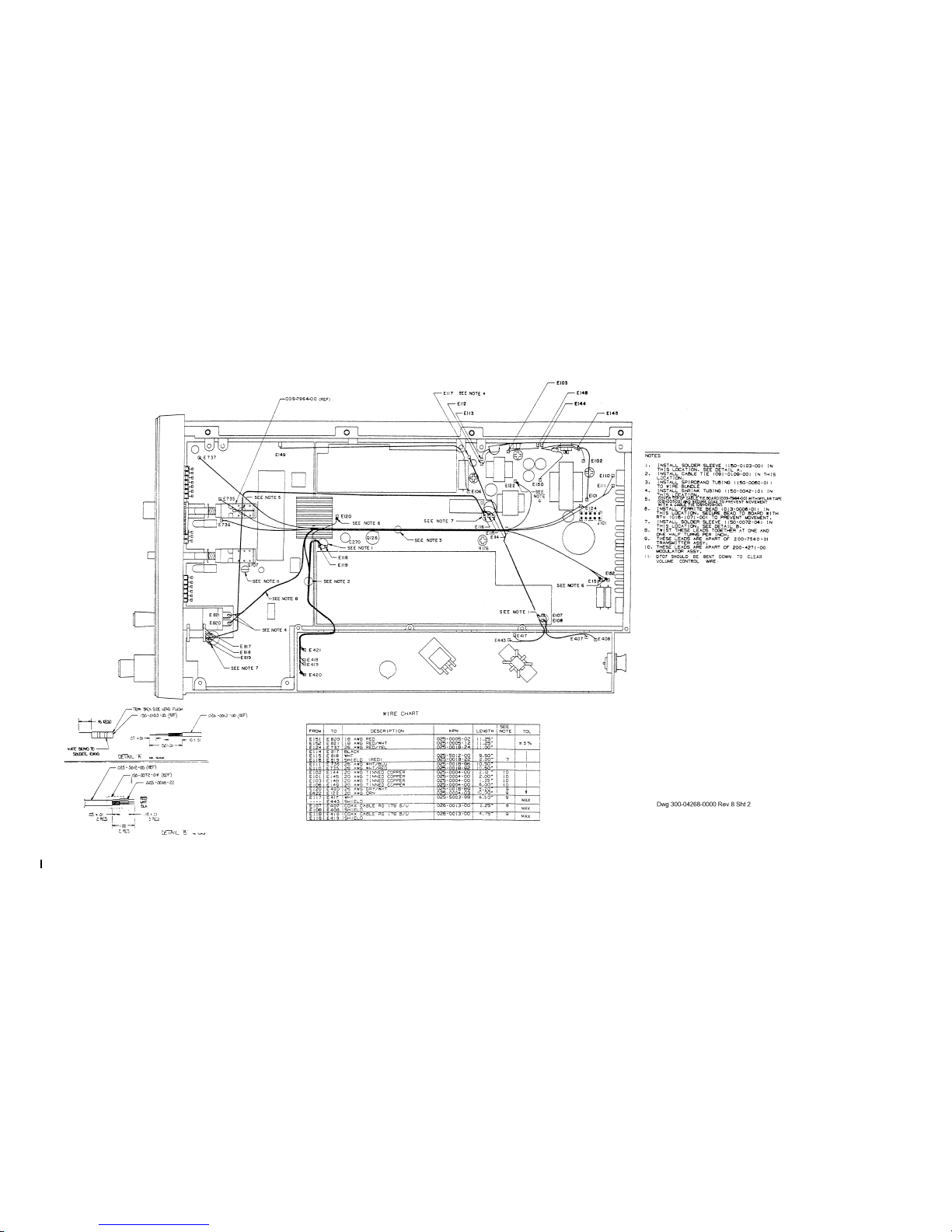
B KY 96A, KY 97A
Rev 5, Apr 2003 MM 006-05674-0005.dwd Page 6-39
FIGURE 6-1C KY 96A Final Assembly (Sht 2 of 2)
(Dwg No 300-04268-0000, Rev 8, Sht 2)
Page 71

B KY 96A, KY 97A
6.4.2 KY 97A VHF Communication Transceiver
064-01051-0010 97A 25 KHZ SEL REV AB
064-01051-0011 97A 50 KHZ SEL REV AB
064-01051-0030 97A 25K SEL 136975 REV AB
064-01051-0099 COMMON BOM REV AD
-----------------------------------------------------------------------------------SYMBOL PART NUMBER FIND NO DESCRIPTION UM -0010 -0011 -0030 -0099
-----------------------------------------------------------------------------------I108 120-03026-0000 IC MC7805CT EA . . . 1.00
Q113 007-00930-0000 XSTR S PNPMJE15029 EA . . . 1.00
Q125 007-00525-0000 XSTR PWR MJE15028 EA . . . 1.00
REF1 300-04268-0001 KY97A COMM TRANSC RF . . . .00
REF100 000-00601-0003 PRODUCT STRUCTURE RF . . . .00
012-01005-0002 TAPE MYLAR .500 W IN . . . .50
012-01127-0000 TAG COVER EA . . . 4.00
013-00006-0001 FERR BEAD EA . . . 4.00
016-01008-0004 GLYPTAL 7526 BL AR . . . 1.00
016-01015-0000 IND ADH 3M 4475 AR . . . 1.00
016-01071-0000 DC RTV 3140 AR . . . 1.00
025-00005-0002 WIRE 18 RED IN . . . 11.25
025-00005-0012 WIRE 18 RD/WH IN . . . 9.00
025-00018-0022 WIRE 26 RED IN . . . 2.00
025-00018-0024 WIRE 26 RD/YL IN . . . 11.00
025-00018-0092 WIRE 26 WH/RD IN . . . 10.50
025-00018-0096 WIRE 26 WH/BU IN . . . 10.50
025-05012-0000 WIRE 2C SHD WHTBLK IN . . . 9.50
030-02229-0011 RGT ANG HDR 3P EA . . . 1.00
030-02229-0013 RGT ANG HDR 7P EA . . . 1.00
030-02229-0014 RGT ANG HDR 6P EA . . . 1.00
035-01007-0020 CONN CVR NAS820-8 EA . . . 1.00
035-01361-0020 PROTECTIVE COVER EA . . . 1.00
047-04811-0001 COVER XMTR W/F EA . . . 1.00
047-08494-0501 TOP COVER ASSEMBLY EA 1.00 1.00 1.00 .
047-08495-0002 COVER, BOTTOM EA . . . 1.00
047-08512-0004 MOUNTING RACK EA . . . 1.00
057-01540-0000 WARNING HV TAG EA . . . 1.00
057-02203-1010 S/N TAG FLVR BLK EA 1.00 . . .
057-02203-1011 S/N TAG FLVR BLK EA . 1.00 . .
057-02203-1030 S/N TAG FLVR BLK EA . . 1.00 .
057-02312-0001 DECAL EA . 1.00 . .
057-02337-0000 PRTCTV CVR DECAL EA . . . 1.00
057-03452-0001 S/N TAG KY97A EA . . . 1.00
057-03511-0001 DECAL, CAUTION EA . . . 1.00
064-01051-0099 COMMON BOM EA 1.00 1.00 1.00 .
073-00808-0003 KNOB VOLUME EA . . . 1.00
088-00838-0006 PUSH BUTTON EA . . . 1.00
088-02269-0005 BEZEL LCD EA . . . 1.00
088-02270-0000 PUSH BUTTON, RND EA . . . 1.00
088-02271-0000 LIGHTING SHAFT EA . . . 1.00
089-05434-0003 SCR FHP 3-48X3/16 EA . . . 9.00
089-05434-0004 SCR FHP 3-48X1/4 EA . . . 8.00
089-05874-0005 SCR PHP 2-56X5/16 EA . . . 1.00
089-05899-0003 SCR PHP 2-56X3/16 EA . . . 1.00
089-05901-0004 SCR PHP 3-48X1/4 EA . . . 7.00
089-05903-0004 SCR PHP 4-40X1/4 EA . . . 3.00
089-05925-0004 SCR BHP 3-48X1/4 EA . . . 5.00
089-06298-0004 SCR FHP 3-48X1/4 EA . . . 2.00
089-06342-0004 SCR PHP 3-48X1/4 EA . . . 4.00
090-00991-0000 PROTECTIVE CLOSURE EA . . . 1.00
091-00109-0000 CABLE TIE EA . . . 2.00
091-00156-0000 BUSHING EA . . . 3.00
091-00286-0002 INSUL XSTR .687 EA . . . 2.00
150-00049-0010 SHRINK TUBING WHT IN . . . 1.25
150-00060-0001 SPIROBAND IN . . . 5.25
Rev 5, Apr 2003 MM 006-05674-0005.dwd Page 6-41
Page 72

B KY 96A, KY 97A
-----------------------------------------------------------------------------------SYMBOL PART NUMBER FIND NO DESCRIPTION UM -0010 -0011 -0030 -0099
----------------------------------------------------------------------------------- 150-00072-0004 SLDR SLEEVE .62 EA . . . 2.00
150-00103-0000 SLDR SLEEVE EA . . . 2.00
200-04270-0000 14V MODULATOR ASSY EA . . . 1.00
200-07479-0000 LCD DISPLAY BD EA . . . 1.00
200-07540-0000 KY97A 14V 5W TX BD EA . . . 1.00
200-07799-0020 97A MNBD 25K FUJI EA 1.00 . 1.00 .
200-07799-0022 97A MN BD 50K FUJI EA . 1.00 . .
206-00021-0020 TOP SW BOM, KY96A/ EA 1.00 1.00 . .
206-00022-0020 TOP SW BOM, KY96A/ EA . . 1.00 .
Rev 5, Apr 2003 MM 006-05674-0005.dwd Page 6-42
Page 73

B KY 96A, KY 97A
064-01051-0031 97A 50K SEL 136975 REV AB
064-01051-0050 97A 25KHZ W/AUDAMP REV AB
064-01051-0051 97A 50KHZ W/AUDAMP REV AB
064-01051-0099 COMMON BOM REV AD
-----------------------------------------------------------------------------------SYMBOL PART NUMBER FIND NO DESCRIPTION UM -0031 -0050 -0051 -0099
-----------------------------------------------------------------------------------I108 120-03026-0000 IC MC7805CT EA . . . 1.00
Q113 007-00930-0000 XSTR S PNPMJE15029 EA . . . 1.00
Q125 007-00525-0000 XSTR PWR MJE15028 EA . . . 1.00
REF1 300-04268-0001 KY97A COMM TRANSC RF . . . .00
REF100 000-00601-0003 PRODUCT STRUCTURE RF . . . .00
012-01005-0002 TAPE MYLAR .500 W IN . . . .50
012-01127-0000 TAG COVER EA . . . 4.00
013-00006-0001 FERR BEAD EA . . . 4.00
016-01008-0004 GLYPTAL 7526 BL AR . . . 1.00
016-01015-0000 IND ADH 3M 4475 AR . . . 1.00
016-01071-0000 DC RTV 3140 AR . . . 1.00
025-00005-0002 WIRE 18 RED IN . . . 11.25
025-00005-0012 WIRE 18 RD/WH IN . . . 9.00
025-00018-0022 WIRE 26 RED IN . . . 2.00
025-00018-0024 WIRE 26 RD/YL IN . . . 11.00
025-00018-0092 WIRE 26 WH/RD IN . . . 10.50
025-00018-0096 WIRE 26 WH/BU IN . . . 10.50
025-05012-0000 WIRE 2C SHD WHTBLK IN . . . 9.50
030-02229-0011 RGT ANG HDR 3P EA . . . 1.00
030-02229-0013 RGT ANG HDR 7P EA . . . 1.00
030-02229-0014 RGT ANG HDR 6P EA . . . 1.00
035-01007-0020 CONN CVR NAS820-8 EA . . . 1.00
035-01361-0020 PROTECTIVE COVER EA . . . 1.00
047-04811-0001 COVER XMTR W/F EA . . . 1.00
047-08494-0501 TOP COVER ASSEMBLY EA 1.00 . . .
047-08495-0002 COVER, BOTTOM EA . . . 1.00
047-08512-0004 MOUNTING RACK EA . . . 1.00
047-12516-0501 TOP COVER ASSY EA . 1.00 1.00 .
057-01540-0000 WARNING HV TAG EA . . . 1.00
057-02203-1031 S/N TAG FLVR BLK EA 1.00 . . .
057-02203-1050 S/N TAG FLVR BLK EA . 1.00 . .
057-02203-1051 S/N TAG FLVR BLK EA . . 1.00 .
057-02312-0001 DECAL EA 1.00 . 1.00 .
057-02337-0000 PRTCTV CVR DECAL EA . . . 1.00
057-03452-0001 S/N TAG KY97A EA . . . 1.00
057-03511-0001 DECAL, CAUTION EA . . . 1.00
064-01051-0099 COMMON BOM EA 1.00 1.00 1.00 .
073-00808-0003 KNOB VOLUME EA . . . 1.00
088-00838-0006 PUSH BUTTON EA . . . 1.00
088-02269-0005 BEZEL LCD EA . . . 1.00
088-02270-0000 PUSH BUTTON, RND EA . . . 1.00
088-02271-0000 LIGHTING SHAFT EA . . . 1.00
089-05434-0003 SCR FHP 3-48X3/16 EA . . . 9.00
089-05434-0004 SCR FHP 3-48X1/4 EA . . . 8.00
089-05874-0005 SCR PHP 2-56X5/16 EA . . . 1.00
089-05899-0003 SCR PHP 2-56X3/16 EA . . . 1.00
089-05901-0004 SCR PHP 3-48X1/4 EA . . . 7.00
089-05903-0004 SCR PHP 4-40X1/4 EA . . . 3.00
089-05925-0004 SCR BHP 3-48X1/4 EA . . . 5.00
089-06004-0003 SCR FHP 2-56X3/16 EA . 5.00 5.00 .
089-06298-0004 SCR FHP 3-48X1/4 EA . . . 2.00
089-06342-0004 SCR PHP 3-48X1/4 EA . . . 4.00
090-00991-0000 PROTECTIVE CLOSURE EA . . . 1.00
091-00109-0000 CABLE TIE EA . . . 2.00
091-00156-0000 BUSHING EA . . . 3.00
091-00286-0002 INSUL XSTR .687 EA . . . 2.00
150-00049-0010 SHRINK TUBING WHT IN . . . 1.25
150-00060-0001 SPIROBAND IN . . . 5.25
150-00072-0004 SLDR SLEEVE .62 EA . . . 2.00
Rev 5, Apr 2003 MM 006-05674-0005.dwd Page 6-43
Page 74

B KY 96A, KY 97A
-----------------------------------------------------------------------------------SYMBOL PART NUMBER FIND NO DESCRIPTION UM -0031 -0050 -0051 -0099
----------------------------------------------------------------------------------- 150-00103-0000 SLDR SLEEVE EA . . . 2.00
200-04270-0000 14V MODULATOR ASSY EA . . . 1.00
200-07479-0000 LCD DISPLAY BD EA . . . 1.00
200-07540-0000 KY97A 14V 5W TX BD EA . . . 1.00
200-07797-0000 AUDIO AMP BOARD EA . 1.00 1.00 .
200-07799-0020 97A MNBD 25K FUJI EA . 1.00 . .
200-07799-0022 97A MN BD 50K FUJI EA 1.00 . 1.00 .
206-00021-0020 TOP SW BOM, KY96A/ EA . 1.00 1.00 .
206-00022-0020 TOP SW BOM, KY96A/ EA 1.00 . . .
Rev 5, Apr 2003 MM 006-05674-0005.dwd Page 6-44
Page 75

B KY 96A, KY 97A
064-01051-0060 97A25KHZ36975W/AMP REV AB
064-01051-0061 97A50KHZ36975W/AMP REV AB
064-01051-0070 KY97A FINAL ASSY REV AF
064-01051-0099 COMMON BOM REV AD
-----------------------------------------------------------------------------------SYMBOL PART NUMBER FIND NO DESCRIPTION UM -0060 -0061 -0070 -0099
-----------------------------------------------------------------------------------I108 120-03026-0000 IC MC7805CT EA . . 1.00 1.00
Q113 007-00930-0000 XSTR S PNPMJE15029 EA . . 1.00 1.00
Q125 007-00525-0000 XSTR PWR MJE15028 EA . . 1.00 1.00
REF1 300-04268-0001 KY97A COMM TRANSC RF . . .00 .00
REF100 000-00601-0003 PRODUCT STRUCTURE RF . . .00 .00
012-01005-0002 TAPE MYLAR .500 W IN . . .50 .50
012-01127-0000 TAG COVER EA . . 4.00 4.00
013-00006-0001 FERR BEAD EA . . 4.00 4.00
016-01008-0004 GLYPTAL 7526 BL AR . . 1.00 1.00
016-01015-0000 IND ADH 3M 4475 AR . . 1.00 1.00
016-01071-0000 DC RTV 3140 AR . . 1.00 1.00
025-00005-0002 WIRE 18 RED IN . . 11.25 11.25
025-00005-0012 WIRE 18 RD/WH IN . . 9.00 9.00
025-00018-0022 WIRE 26 RED IN . . 2.00 2.00
025-00018-0024 WIRE 26 RD/YL IN . . 11.00 11.00
025-00018-0092 WIRE 26 WH/RD IN . . 10.50 10.50
025-00018-0096 WIRE 26 WH/BU IN . . 10.50 10.50
025-05012-0000 WIRE 2C SHD WHTBLK IN . . 9.50 9.50
030-02229-0011 RGT ANG HDR 3P EA . . 1.00 1.00
030-02229-0013 RGT ANG HDR 7P EA . . 1.00 1.00
030-02229-0014 RGT ANG HDR 6P EA . . 1.00 1.00
035-01007-0020 CONN CVR NAS820-8 EA . . 1.00 1.00
035-01361-0020 PROTECTIVE COVER EA . . 1.00 1.00
047-04811-0001 COVER XMTR W/F EA . . 1.00 1.00
047-08495-0002 COVER, BOTTOM EA . . 1.00 1.00
047-08512-0004 MOUNTING RACK EA . . 1.00 1.00
047-12516-0501 TOP COVER ASSY EA 1.00 1.00 1.00 .
057-01540-0000 WARNING HV TAG EA . . 1.00 1.00
057-02203-1060 S/N TAG FLVR BLK EA 1.00 . . .
057-02203-1061 S/N TAG FLVR BLK EA . 1.00 . .
057-02203-1070 S/N TAG FLVR BLK EA . . 1.00 .
057-02312-0001 DECAL EA . 1.00 . .
057-02337-0000 PRTCTV CVR DECAL EA . . 1.00 1.00
057-03452-0001 S/N TAG KY97A EA . . 1.00 1.00
057-03511-0001 DECAL, CAUTION EA . . 1.00 1.00
064-01051-0099 COMMON BOM EA 1.00 1.00 . .
073-00808-0003 KNOB VOLUME EA . . . 1.00
073-00972-0003 KNOB VOLUME EA . . 1.00 .
088-00838-0006 PUSH BUTTON EA . . . 1.00
088-00838-0050 LIGHTING SHAFT EA . . 1.00 .
088-02269-0005 BEZEL LCD EA . . . 1.00
088-02270-0000 PUSH BUTTON, RND EA . . . 1.00
088-02270-0001 PUSH BUTTON EA . . 1.00 .
088-02271-0000 LIGHTING SHAFT EA . . 1.00 1.00
088-03101-0010 BEZEL COMPL KY97A EA . . 1.00 .
088-03130-0001 TRANSFER BUTTON EA . . 1.00 .
089-05434-0003 SCR FHP 3-48X3/16 EA . . 9.00 9.00
089-05434-0004 SCR FHP 3-48X1/4 EA . . 8.00 8.00
089-05874-0005 SCR PHP 2-56X5/16 EA . . 1.00 1.00
089-05899-0003 SCR PHP 2-56X3/16 EA . . 1.00 1.00
089-05901-0004 SCR PHP 3-48X1/4 EA . . 7.00 7.00
089-05903-0004 SCR PHP 4-40X1/4 EA . . 3.00 3.00
089-05925-0004 SCR BHP 3-48X1/4 EA . . 5.00 5.00
089-06004-0003 SCR FHP 2-56X3/16 EA 5.00 5.00 5.00 .
089-06298-0004 SCR FHP 3-48X1/4 EA . . 2.00 2.00
089-06342-0004 SCR PHP 3-48X1/4 EA . . 4.00 4.00
090-00991-0000 PROTECTIVE CLOSURE EA . . 1.00 1.00
091-00109-0000 CABLE TIE EA . . 2.00 2.00
091-00156-0000 BUSHING EA . . 3.00 3.00
Rev 5, Apr 2003 MM 006-05674-0005.dwd Page 6-45
Page 76

B KY 96A, KY 97A
-----------------------------------------------------------------------------------SYMBOL PART NUMBER FIND NO DESCRIPTION UM -0060 -0061 -0070 -0099
----------------------------------------------------------------------------------- 091-00286-0002 INSUL XSTR .687 EA . . 2.00 2.00
150-00049-0010 SHRINK TUBING WHT IN . . 1.25 1.25
150-00060-0001 SPIROBAND IN . . 5.25 5.25
150-00072-0004 SLDR SLEEVE .62 EA . . 2.00 2.00
150-00103-0000 SLDR SLEEVE EA . . 2.00 2.00
200-04270-0000 14V MODULATOR ASSY EA . . 1.00 1.00
200-07479-0000 LCD DISPLAY BD EA . . . 1.00
200-07479-0001 LCD DISPLAY BD EA . . 1.00 .
200-07540-0000 KY97A 14V 5W TX BD EA . . 1.00 1.00
200-07797-0000 AUDIO AMP BOARD EA 1.00 1.00 1.00 .
200-07799-0020 97A MNBD 25K FUJI EA 1.00 . 1.00 .
200-07799-0022 97A MN BD 50K FUJI EA . 1.00 . .
206-00022-0020 TOP SW BOM, KY96A/ EA 1.00 1.00 1.00 .
Rev 5, Apr 2003 MM 006-05674-0005.dwd Page 6-46
Page 77
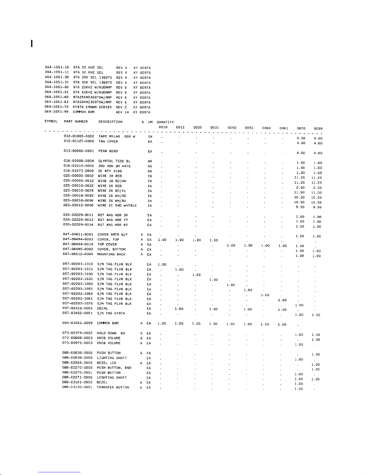
B KY 96A, KY 97A
THIS PAGE CONTAINS OLD REVISION BOMS, FOR REFERENCE ONLY.
Rev 5, Apr 2003 MM 006-05674-0005.dwd Page 6-47
Page 78
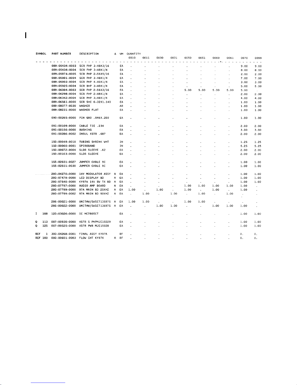
B KY 96A, KY 97A
THIS PAGE CONTAINS OLD REVISION BOMS, FOR REFERENCE ONLY.
Rev 5, Apr 2003 MM 006-05674-0005.dwd Page 6-48
Page 79
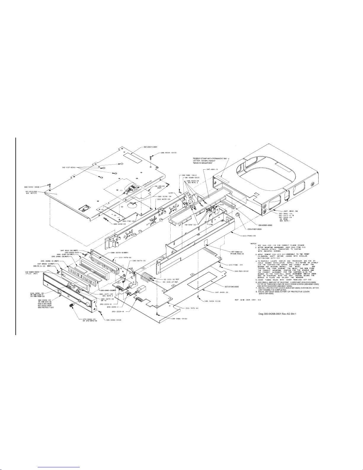
B KY 96A, KY 97A
Rev 5, Apr 2003 MM 006-05674-0005.dwd Page 6-49
FIGURE 6-2 KY 97A Final Assembly (Sht 1 of 2)
(Dwg No 300-04268-0001, Rev AG, Sht 1)
Page 80
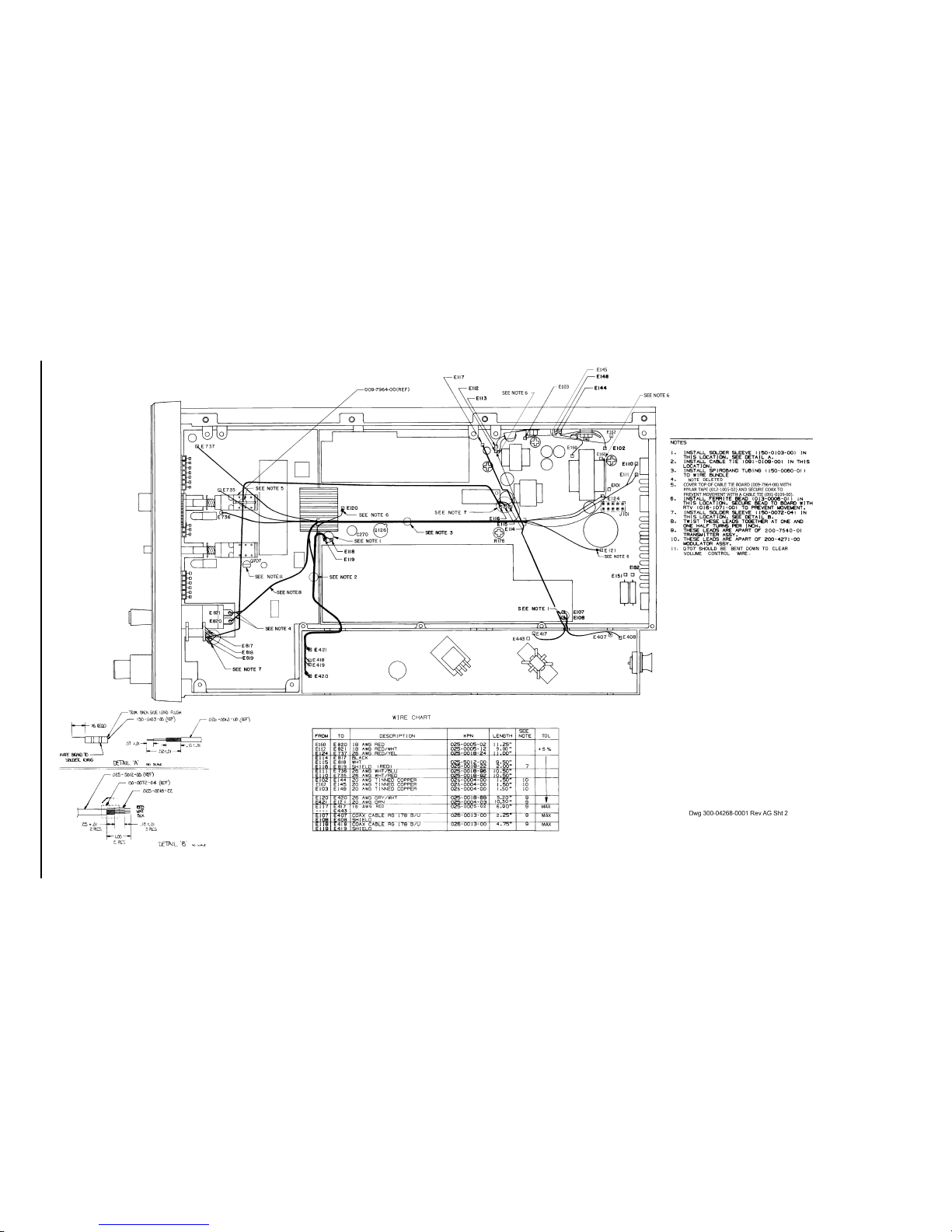
B KY 96A, KY 97A
Rev 5, Apr 2003 MM 006-05674-0005.dwd Page 6-51
FIGURE 6-2 KY 97A Final Assembly (Sht 2 of 2)
(Dwg No 300-04268-0001, Rev AG, Sht 2)
Page 81

B KY 96A, KY 97A
6.4.3 KY 96A, KY 97A Unit Software Set
206-00021-0020 TOP SW BOM, KY96A/97A REV 206-00022-0020 TOP SW BOM, KY96A/97A REV -
---------------------------------------------------------------------SYMBOL PART NUMBER FIND NO DESCRIPTION UM -0020 -0020
--------------------------------------------------------------------- 057-03284-0020 SCM TAG EA 1.00 1.00
205-00506-0020 BOARD HW/SW SET, K EA 1.00 .
205-00507-0020 BOARD HW/SW SET, EA . 1.00
205-00506-0020 BOARD HW/SW SET, KY96A/97A REV 205-00507-0020 BOARD HW/SW SET, KY96A/97A REV -
---------------------------------------------------------------------SYMBOL PART NUMBER FIND NO DESCRIPTION UM -0020 -0020
--------------------------------------------------------------------- 057-05252-0506 IDT 206-00506-00XX EA 1.00 .
057-05252-0507 IDT 206-00507-00XX EA . 1.00
057-05335-0020 DECAL 205 DASH 20 EA 1.00 1.00
125-00241-0020 SOFTWARE SET EA 1.00 1.00
200-07475-0000 LCD PROCESSOR BD EA 1.00 .
200-07475-0001 LCD PROC 136.975 EA . 1.00
125-00241-0020 SOFTWARE SET REV A
--------------------------------------------------------------SYMBOL PART NUMBER FIND NO DESCRIPTION UM -0020
-------------------------------------------------------------- 122-00605-0020 122-00605-0020 IS EA 1.00
NOTE: Programmed chip P/N 122-00605-0020 = I702.
Rev 5, Apr 2003 MM 006-05674-0005.dwd Page 6-53
Page 82

B KY 96A, KY 97A
THIS PAGE RESERVED
Rev 5, Apr 2003 MM 006-05674-0005.dwd Page 6-54
Page 83
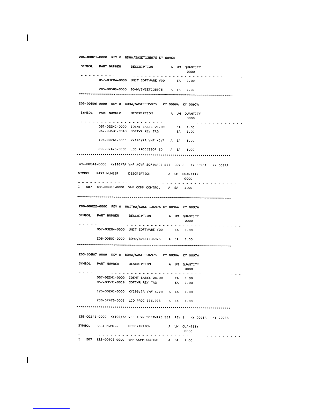
B KY 96A, KY 97A
THIS PAGE CONTAINS OLD REVISION BOMS, FOR REFERENCE ONLY.
NOTE: Programmed chip P/N 122-00605-0000 is actually I702.
Rev 5, Apr 2003 MM 006-05674-0005.dwd Page 6-55
Page 84

B KY 96A, KY 97A
THIS PAGE RESERVED
Rev 5, Apr 2003 MM 006-05674-0005.dwd Page 6-56
Page 85

B KY 96A, KY 97A
6.4.4 LCD Processor Board
200-07475-0000 LCD PROCESSOR BD REV 0
200-07475-0001 LCD PROC 136.975 REV 1
200-07475-0099 LCD PROC COMMON REV AB
----------------------------------------------------------------------------SYMBOL PART NUMBER FIND NO DESCRIPTION UM -0000 -0001 -0099
----------------------------------------------------------------------------C701 106-04121-0026 CAPCH120PFNPO/100V EA . . 1.00
C702 106-04473-0047 CAP CH 47K X7R/50V EA . . 1.00
C703 106-04473-0047 CAP CH 47K X7R/50V EA . . 1.00
C704 097-00108-0007 CAP EL 10UF 16V EA . . 1.00
C705 106-04473-0047 CAP CH 47K X7R/50V EA . . 1.00
C706 106-04121-0026 CAPCH120PFNPO/100V EA . . 1.00
C707 106-04154-0078 CAP CH 150KZ5U/50V EA . . 1.00
CR701 007-05117-0007 DIO Z 6.2V SOT EA . . 1.00
CR702 007-06025-0000 DIO S 1N4003 EA . . 1.00
CR703 007-06025-0000 DIO S 1N4003 EA . . 1.00
CR704 999-09999-0098 PLACE HOLDER RF . . .00
CR705 999-09999-0098 PLACE HOLDER RF . . .00
CR706 007-06105-0000 DIO HV FDH444 EA . . 1.00
CR707 007-06105-0000 DIO HV FDH444 EA . . 1.00
CR708 007-06223-0000 DIO DUAL SWITCHING EA . . 1.00
CR709 007-06181-0000 DIO DUAL MMBD2835 EA . . 1.00
CR710 007-06181-0000 DIO DUAL MMBD2835 EA . . 1.00
CR711 007-06025-0000 DIO S 1N4003 EA . . 1.00
CR712 007-06025-0000 DIO S 1N4003 EA . . 1.00
DS701 037-00034-0002 LMP 8098 T1 14V EA . . 1.00
DS702 037-00034-0002 LMP 8098 T1 14V EA . . 1.00
I701 120-03163-0001 LM2901 SO-14 COMP EA . . 1.00
I702 122-00605-9999 SOFTWARE PLACEHOLD RF . . .00
I703 120-03127-0011 IC LM2903 SO PKG EA . . 1.00
I704 120-02156-0000 16X16 BIT EEPROM EA . . 1.00
I705 123-04024-0003 IC 74HC4024 SO-14 EA . . 1.00
I706 120-03246-0000 TLC541IFN AID CONV EA . . 1.00
Q701 007-00280-0000 XSTR E176/J176 EA . . 1.00
Q702 007-00466-0000 XSTR S PNP MMBTA56 EA . . 1.00
Q703 007-00467-0000 XSTR S NPN MMBTA06 EA . . 1.00
Q704 007-00467-0000 XSTR S NPN MMBTA06 EA . . 1.00
Q705 007-00466-0000 XSTR S PNP MMBTA56 EA . . 1.00
Q706 007-00467-0000 XSTR S NPN MMBTA06 EA . . 1.00
Q707 007-00454-0000 VMOS PWRFET EA . . 1.00
Q708 007-00179-0001 XSTR SOT23 2N3904 EA . . 1.00
Q709 007-00466-0000 XSTR S PNP MMBTA56 EA . . 1.00
R701 139-02001-0000 RES CHIP 2K EW 1% EA . . 1.00
R702 139-04752-0000 RES CH 47.5K EW 1% EA . . 1.00
R703 139-04752-0000 RES CH 47.5K EW 1% EA . . 1.00
R704 139-01001-0000 RES CHIP 1K EW 1% EA . . 1.00
R705 139-05621-0000 RES CHIP 5.62KEW1% EA . . 1.00
R706 139-04752-0000 RES CH 47.5K EW 1% EA . . 1.00
R707 139-04751-0000 RES CH 4.75K EW 1% EA . . 1.00
R708 139-03011-0000 RES CH 3.01K EW 1% EA . . 1.00
R709 139-04752-0000 RES CH 47.5K EW 1% EA . . 1.00
R710 139-04752-0000 RES CH 47.5K EW 1% EA . . 1.00
R711 139-09092-0000 RES CHIP 90.9KEW1% EA . . 1.00
R712 131-00104-0013 RES CF 100K EW 5% EA . . 1.00
R713 136-08871-0062 RES PF 8.87K EW1% EA . . 1.00
R714 136-04872-0062 RES PF 48.7K EW 1% EA . . 1.00
R715 139-01002-0000 RES CHIP 10K EW 1% EA . . 1.00
R716 139-04752-0000 RES CH 47.5K EW 1% EA . . 1.00
R717 139-04752-0000 RES CH 47.5K EW 1% EA . . 1.00
R718 139-01002-0000 RES CHIP 10K EW 1% EA . . 1.00
R719 139-04752-0000 RES CH 47.5K EW 1% EA . . 1.00
R720 139-04752-0000 RES CH 47.5K EW 1% EA . . 1.00
R721 139-01002-0000 RES CHIP 10K EW 1% EA . . 1.00
Rev 5, Apr 2003 MM 006-05674-0005.dwd Page 6-57
Page 86

B KY 96A, KY 97A
----------------------------------------------------------------------------SYMBOL PART NUMBER FIND NO DESCRIPTION UM -0000 -0001 -0099
----------------------------------------------------------------------------R722 139-04752-0000 RES CH 47.5K EW 1% EA . . 1.00
R723 139-02742-0000 RES CHIP 27.4KEW1% EA . . 1.00
R724 139-04752-0000 RES CH 47.5K EW 1% EA . . 1.00
R725 139-04752-0000 RES CH 47.5K EW 1% EA . . 1.00
R726 999-09999-0098 PLACE HOLDER RF . . .00
R727 139-03322-0000 RES CH 33.2K EW 1% EA . . 1.00
R728 139-01822-0000 RES CHIP 18.2KEW1% EA . . 1.00
R729 139-08252-0000 RES CH 82.5K EW 1% EA . . 1.00
R730 139-01822-0000 RES CHIP 18.2KEW1% EA . . 1.00
R731 139-04752-0000 RES CH 47.5K EW 1% EA . . 1.00
R732 139-04752-0000 RES CH 47.5K EW 1% EA . . 1.00
R733 139-02741-0000 RES CH 2.74K EW 1% EA . . 1.00
R734 139-02741-0000 RES CH 2.74K EW 1% EA . . 1.00
R735 139-02741-0000 RES CH 2.74K EW 1% EA . . 1.00
R736 139-04751-0000 RES CH 4.75K EW 1% EA . . 1.00
R737 139-03922-0000 RES CH 39.2K EW 1% EA . . 1.00
R738 139-06192-0000 RES CH 61.9K EW 1% EA . . 1.00
R739 139-01001-0000 RES CHIP 1K EW 1% EA . . 1.00
R740 139-04752-0000 RES CH 47.5K EW 1% EA . . 1.00
R741 139-04752-0000 RES CH 47.5K EW 1% EA . . 1.00
R742 139-04752-0000 RES CH 47.5K EW 1% EA . . 1.00
R743 139-04752-0000 RES CH 47.5K EW 1% EA . . 1.00
R744 139-01002-0000 RES CHIP 10K EW 1% EA . . 1.00
R745 139-01002-0000 RES CHIP 10K EW 1% EA . . 1.00
R746 139-02001-0000 RES CHIP 2K EW 1% EA . . 1.00
R747 139-02001-0000 RES CHIP 2K EW 1% EA . . 1.00
R748 139-01002-0000 RES CHIP 10K EW 1% EA . . 1.00
R749 139-01002-0000 RES CHIP 10K EW 1% EA . . 1.00
R750 139-01003-0000 RES CHIP 100KEW1% EA . . 1.00
R751 139-00100-0000 RES CHIP 10 EW 1% EA . . 1.00
R752 139-01003-0000 RES CHIP 100KEW1% EA . . 1.00
R753 139-00100-0000 RES CHIP 10 EW 1% EA . . 1.00
R754 139-01003-0000 RES CHIP 100KEW1% EA . . 1.00
R755 139-03922-0000 RES CH 39.2K EW 1% EA . . 1.00
R756 999-09999-0098 PLACE HOLDER RF . . .00
R757 999-09999-0098 PLACE HOLDER RF . . .00
R758 139-01002-0000 RES CHIP 10K EW 1% EA . . 1.00
R759 139-05110-0000 RES CH 511 EW 1% EA . . 1.00
R760 139-04752-0000 RES CH 47.5K EW 1% EA . . 1.00
R761 139-09091-0000 RES CH 9.09K EW 1% EA . . 1.00
R762 130-05000-0025 RES CHIP 0 EW CJ EA 1.00 1.00 .
R763 130-05000-0025 RES CHIP 0 EW CJ EA 1.00 . .
R764 139-04752-0000 RES CH 47.5K EW 1% EA . . 1.00
R765 139-01000-0000 RES CHIP 100 EW 1% EA . . 1.00
R766 132-00204-0048 1 WATT 390 OHM EA . . 1.00
R767 132-00204-0034 1 WATT 82 OHM EA . . 1.00
REF1 300-07475-0000 LCD PROC BD ASSY RF . . .00
REF2 002-07475-0000 KY 961/97A LCD PRO RF . . .00
S701 031-00343-0002 SWITCH EA . . 1.00
S702 031-00536-0000 SWITCH MOMENTARY EA . . 1.00
S703 031-00536-0000 SWITCH MOMENTARY EA . . 1.00
TP701 008-00096-0001 TERMINAL TEST PNT EA . . 1.00
TP702 008-00096-0001 TERMINAL TEST PNT EA . . 1.00
009-07475-0000 PC BD LCD PROC BD EA . . 1.00
009-07964-0000 CABLE TIE BD EA . . 1.00
016-01040-0000 COATING TYPE AR AR . . 1.00
016-01122-0000 EPOXY DEVCON 14250 AR . . 1.00
088-03413-0001 SWITCH MOUNTING EA . . 1.00
200-07475-0099 LCD PROC COMMON EA 1.00 1.00 .
Rev 5, Apr 2003 MM 006-05674-0005.dwd Page 6-58
Page 87
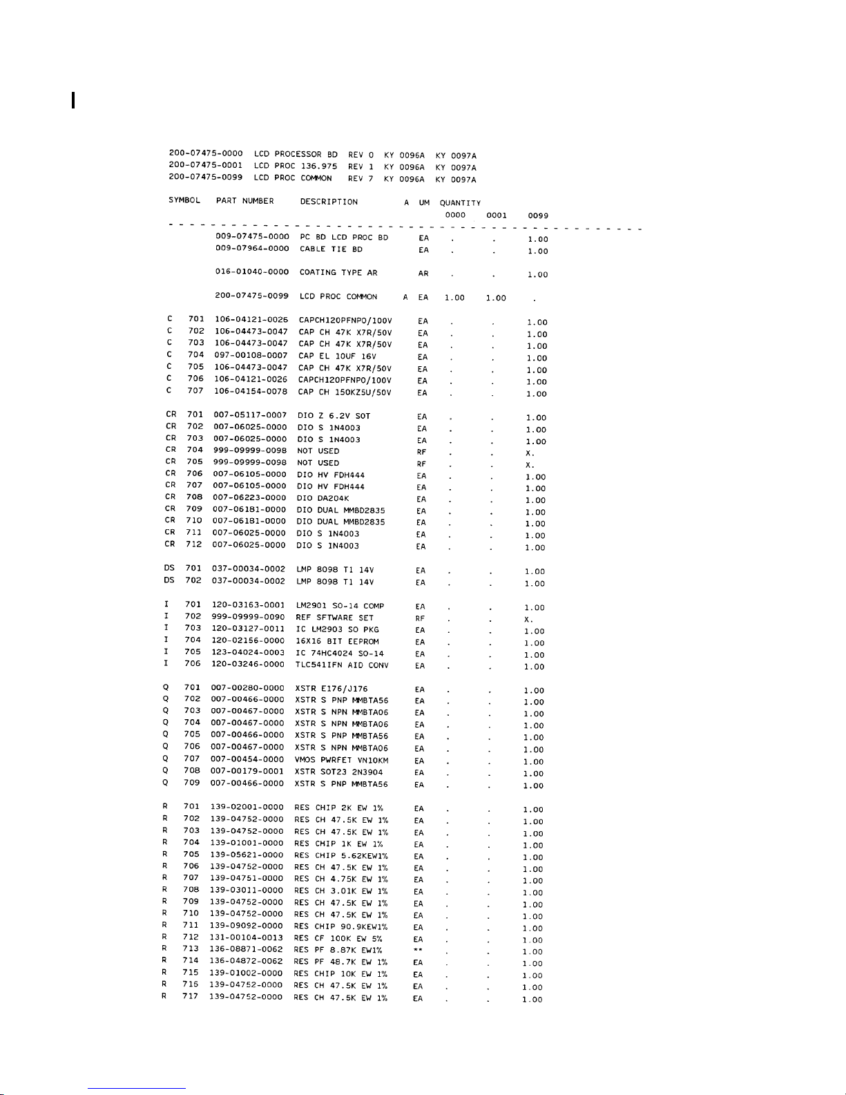
B KY 96A, KY 97A
THIS PAGE CONTAINS OLD REVISION BOMS, FOR REFERENCE ONLY.
Rev 5, Apr 2003 MM 006-05674-0005.dwd Page 6-59
Page 88
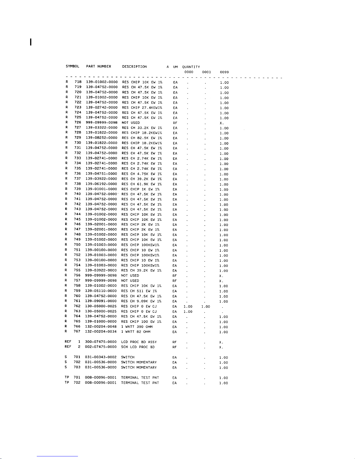
B KY 96A, KY 97A
THIS PAGE CONTAINS OLD REVISION BOMS, FOR REFERENCE ONLY.
Rev 5, Apr 2003 MM 006-05674-0005.dwd Page 6-60
Page 89
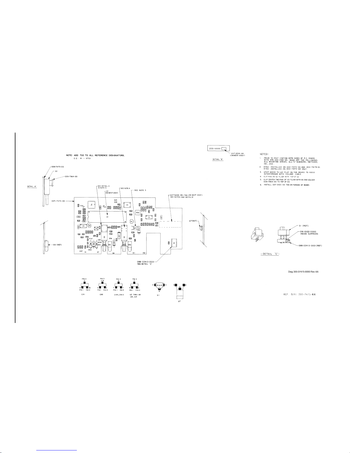
B KY 96A, KY 97A
Rev 5, Apr 2003 MM 006-05674-0005.dwd Page 6-61
FIGURE 6-3 LCD Processor Board Assembly
(Dwg No 300-07475-0000, Rev AA)
Page 90
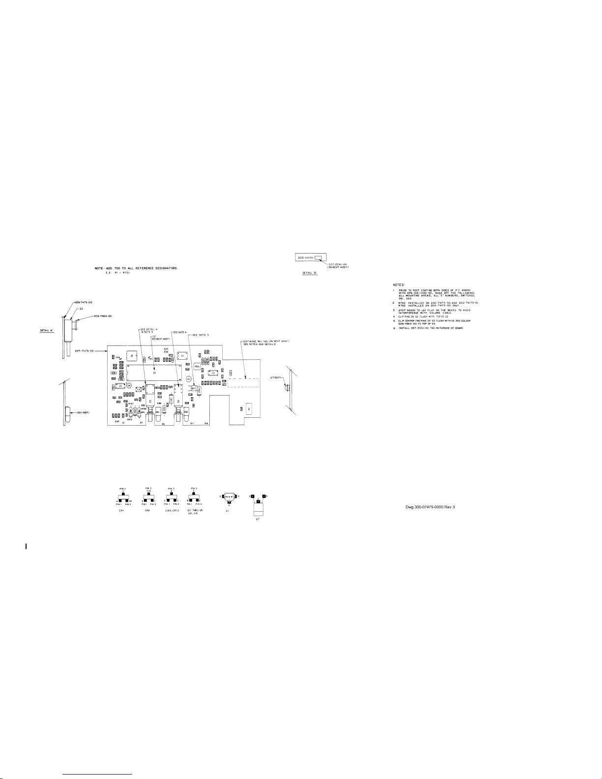
B KY 96A, KY 97A
Rev 5, Apr 2003 MM 006-05674-0005.dwd Page 6-63
FIGURE 6-3A LCD Processor Board Assembly
(Dwg No 300-07475-0000, Rev 3)
Page 91
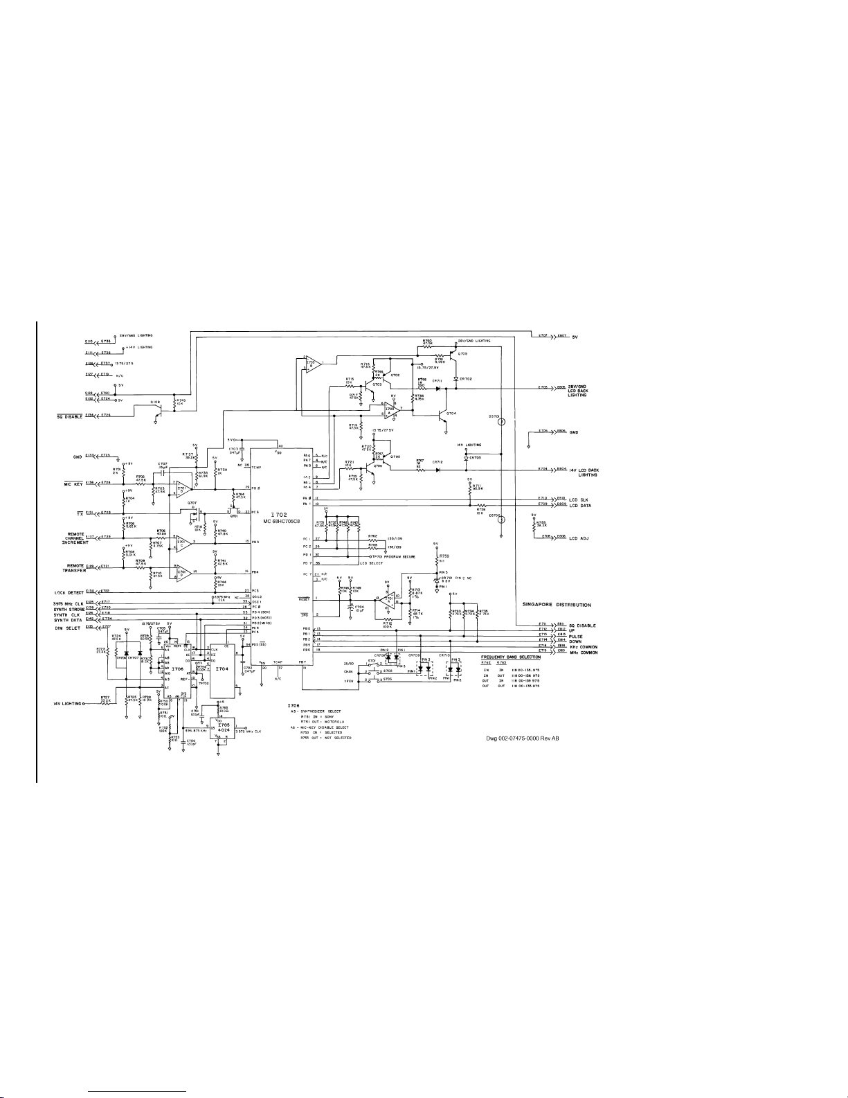
B KY 96A, KY 97A
Rev 5, Apr 2003 MM 006-05674-0005.dwd Page 6-65
FIGURE 6-4 LCD Processor Board Schematic
(Dwg No 002-07475-0000, Rev AB)
Page 92
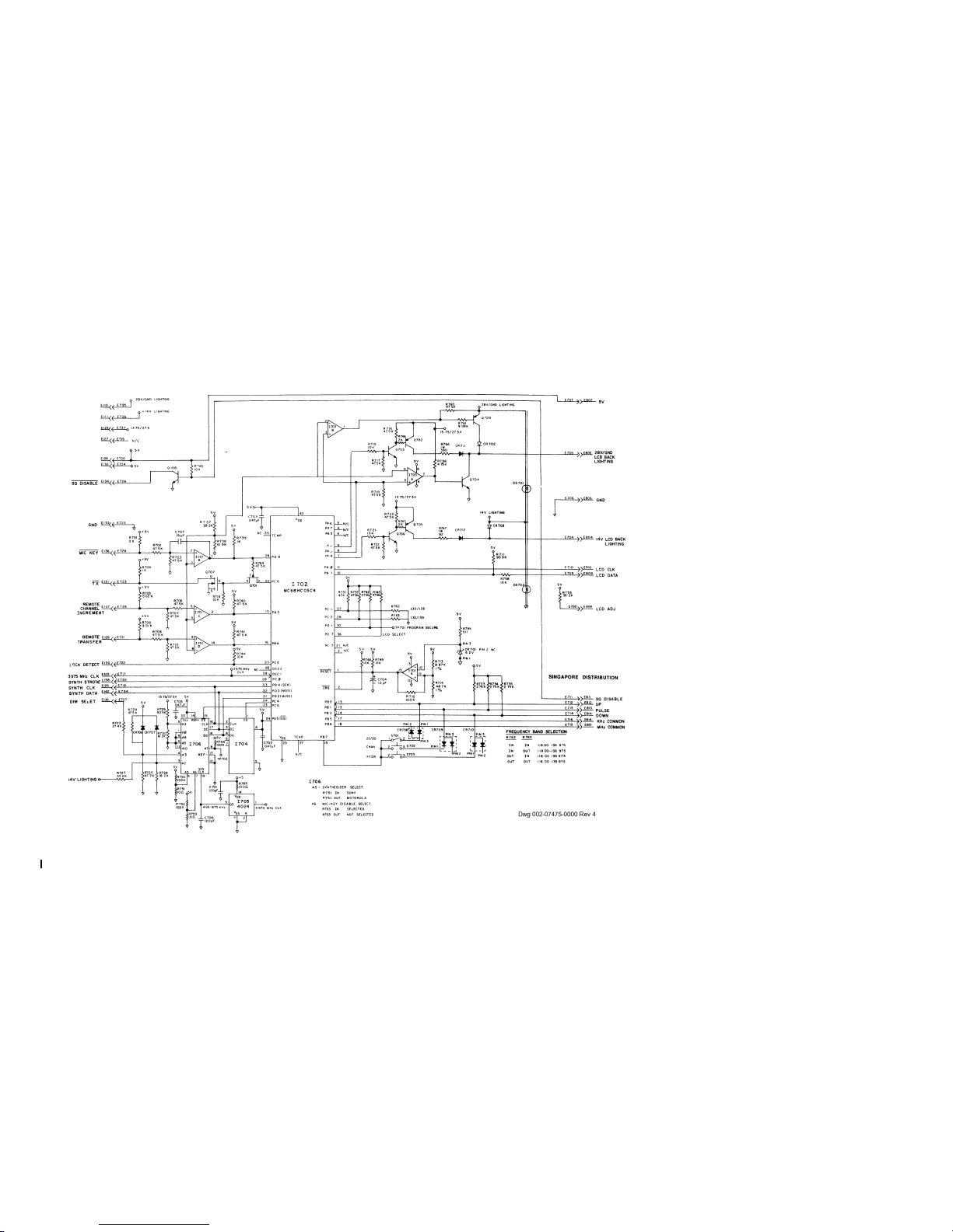
B KY 96A, KY 97A
Rev 5, Apr 2003 MM 006-05674-0005.dwd Page 6-67
FIGURE 6-4A LCD Processor Board Schematic
(Dwg No 002-07475-0000, Rev 4)
Page 93
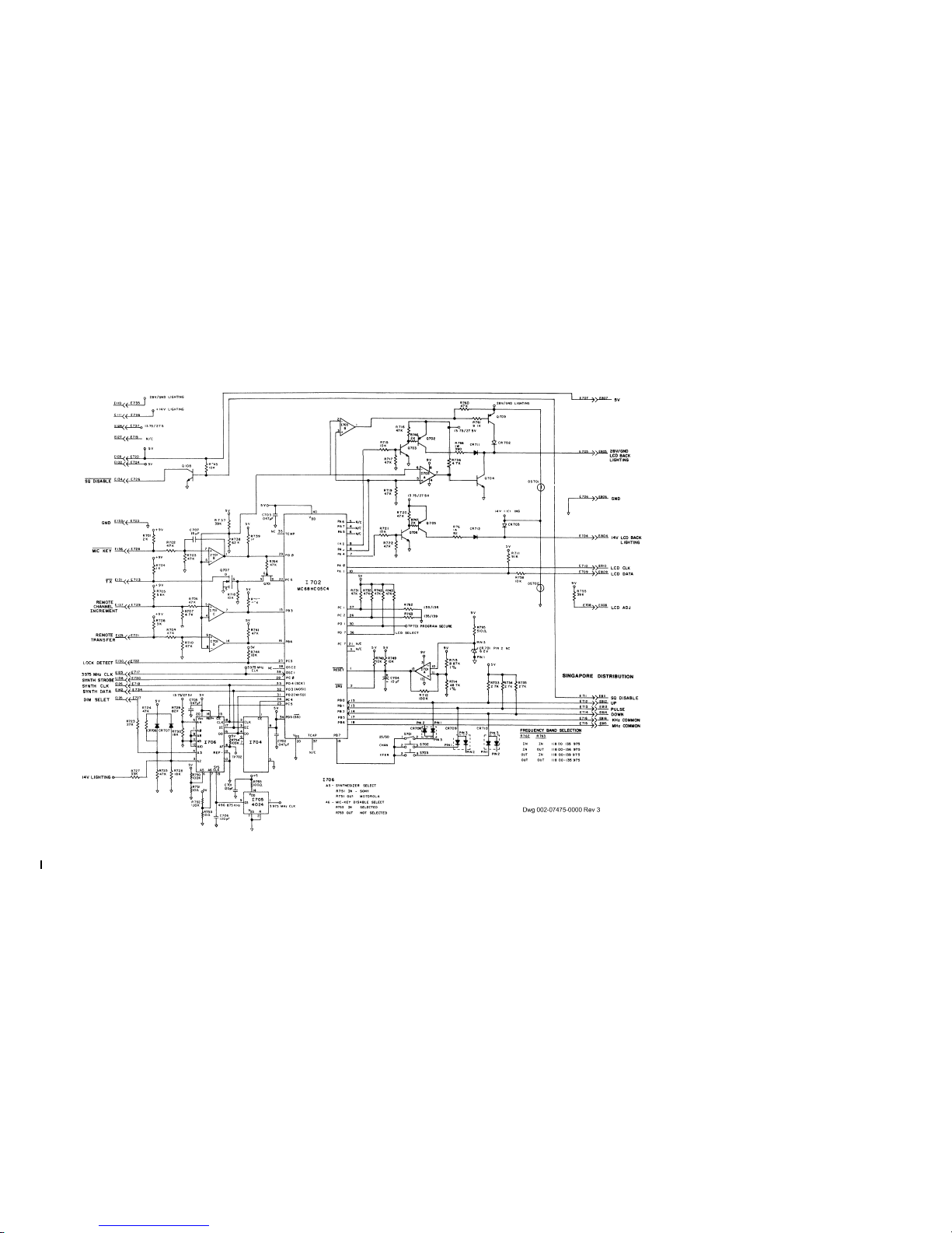
B KY 96A, KY 97A
Rev 5, Apr 2003 MM 006-05674-0005.dwd Page 6-69
FIGURE 6-4B LCD Processor Board Schematic
(Dwg No 002-07475-0000, Rev 3)
Page 94

B KY 96A, KY 97A
6.4.5 KY 97A (14V) Modulator Assembly
200-04270-0000 14V MODULATOR ASSY REV AA
--------------------------------------------------------------SYMBOL PART NUMBER FIND NO DESCRIPTION UM -0000
--------------------------------------------------------------C266 111-00001-0001 CAP CR .1UF 50V EA 1.00
Q124 007-00168-0000 XSTR PNP 2N4398 EA 1.00
REF1 300-04270-0000 COMM TRANSCEIVER K RF .00
RT101 134-01027-0000 POSISTOR BE EA 1.00
008-00050-0001 GND LUG EA 1.00
026-00004-0000 WIRE, CU, 20AWG, T IN 4.50
073-00388-0004 HEAT SINK 196A EA 1.00
076-00159-0000 SPACER INSUL EA 2.00
088-00829-0000 INSL EA 3.00
089-02013-0037 NUT FLAT 6-32 EA 2.00
089-05432-0003 SCR, MACH, 2-56, F EA 6.00
089-05907-0008 SCR PHP 6-32X1/2 EA 2.00
089-08016-0037 WSHR INTL LK #6 EA 1.00
089-08027-0011 WSHR FLT STD #6 EA 1.00
089-08080-0030 WSHR FLT STD .147 EA 2.00
091-00038-0000 WASHER EXT NY EA 2.00
091-00283-0002 TO-3 INSULATOR EA 1.00
150-00003-0010 TUBING TFLN 24AWG IN 4.00
150-00005-0010 TUBING TFLN 20AWG IN 7.25
Rev 5, Apr 2003 MM 006-05674-0005.dwd Page 6-71
Page 95

B KY 96A, KY 97A
THIS PAGE RESERVED
Rev 5, Apr 2003 MM 006-05674-0005.dwd Page 6-72
Page 96
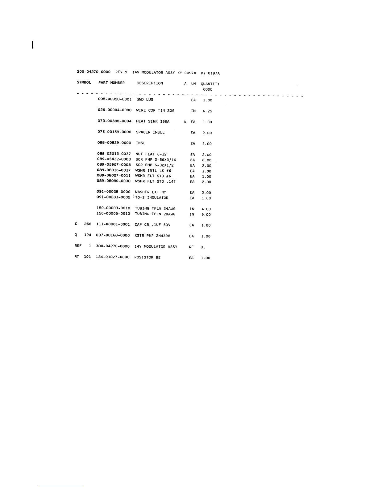
B KY 96A, KY 97A
THIS PAGE CONTAINS OLD REVISION BOMS, FOR REFERENCE ONLY.
Rev 5, Apr 2003 MM 006-05674-0005.dwd Page 6-73
Page 97

B KY 96A, KY 97A
THIS PAGE RESERVED
Rev 5, Apr 2003 MM 006-05674-0005.dwd Page 6-74
Page 98
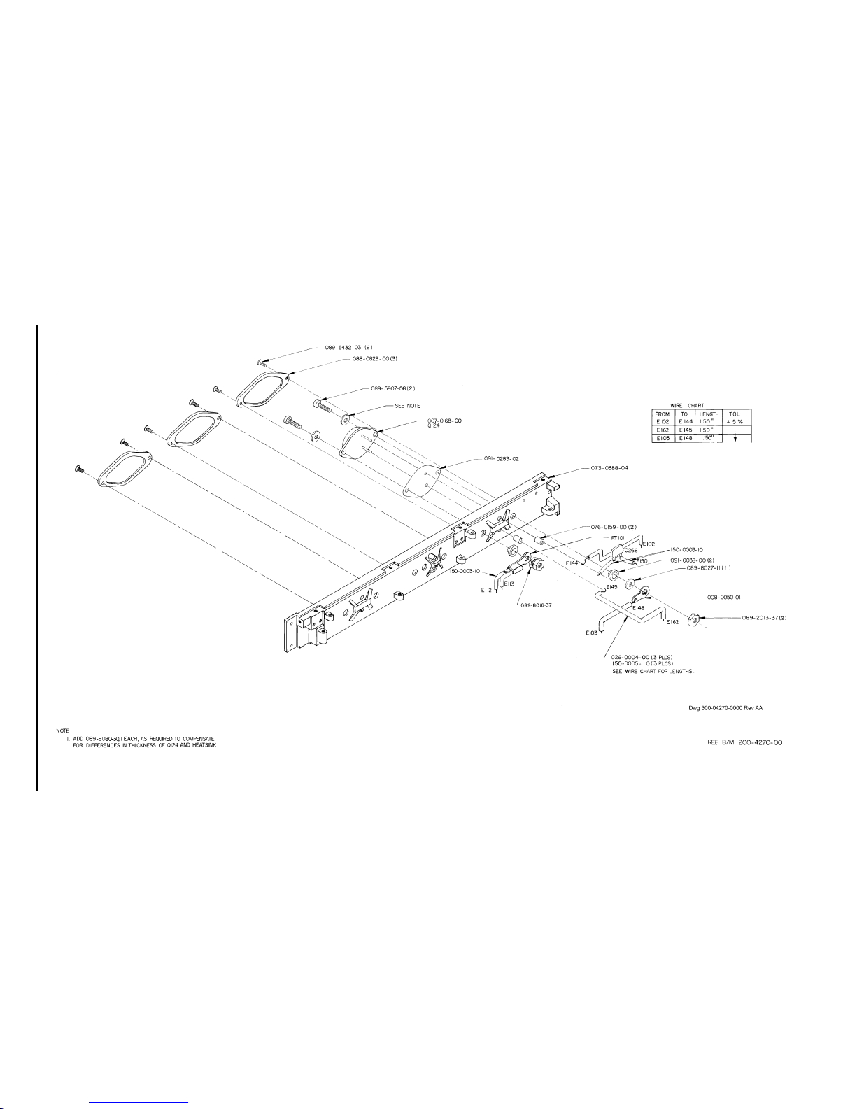
B KY 96A, KY 97A
Rev 5, Apr 2003 MM 006-05674-0005.dwd Page 6-75
FIGURE 6-5 KY 97A (14V) Modulator Assembly
(Dwg No 300-04270-0000, Rev AA)
Page 99
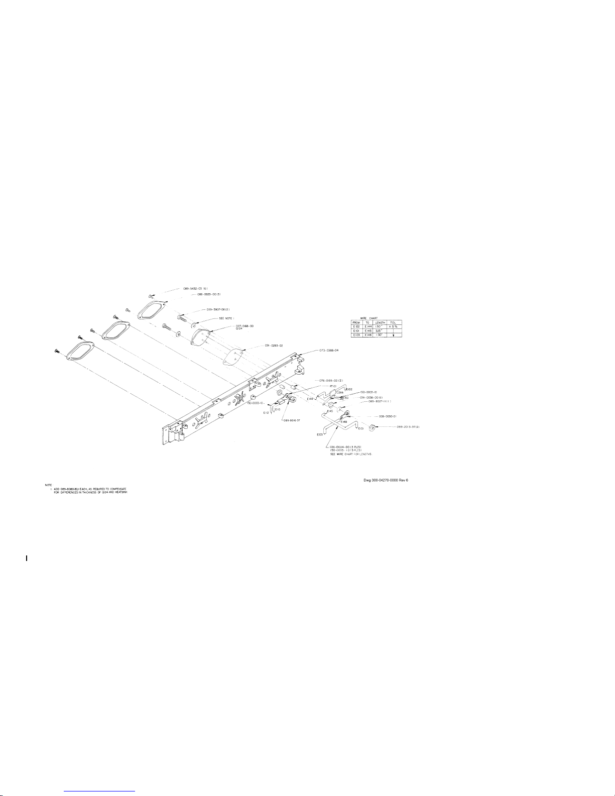
B KY 96A, KY 97A
Rev 5, Apr 2003 MM 006-05674-0005.dwd Page 6-77
FIGURE 6-5A KY 97A (14V) Modulator Assembly
(Dwg No 300-04270-0000, Rev 6)
Page 100

B KY 96A, KY 97A
6.4.6 KY 96A (28V) Modulator Assembly
200-04271-0000 28V MODULATOR ASSY REV AA
--------------------------------------------------------------SYMBOL PART NUMBER FIND NO DESCRIPTION UM -0000
--------------------------------------------------------------C266 111-00001-0001 CAP CR .1UF 50V EA 1.00
Q124 007-00963-0000 XSTR MJ11012 NPN EA 1.00
Q130 007-00963-0000 XSTR MJ11012 NPN EA 1.00
REF1 300-04271-0000 COMM TRANSCEIVER K RF .00
RT101 134-01027-0001 POSISTOR BD EA 1.00
008-00041-0000 SLDR LUG, DUEL EA 1.00
008-00050-0001 GND LUG EA 1.00
026-00004-0000 WIRE, CU, 20AWG, T IN 23.00
073-00388-0004 HEAT SINK 196A EA 1.00
076-00159-0000 SPACER INSUL EA 4.00
076-01063-0000 NYLON HEX NUT EA 1.00
088-00829-0000 INSL EA 3.00
089-02013-0037 NUT FLAT 6-32 EA 3.00
089-05432-0003 SCR, MACH, 2-56, F EA 6.00
089-05907-0006 SCR PHP 6-32X3/8 EA 1.00
089-05907-0008 SCR PHP 6-32X1/2 EA 3.00
089-08016-0037 WSHR INTL LK #6 EA 1.00
089-08027-0011 WSHR FLT STD #6 EA 2.00
089-08080-0030 WSHR FLT STD .147 AR 4.00
091-00038-0000 WASHER EXT NY EA 3.00
091-00283-0002 TO-3 INSULATOR EA 2.00
150-00003-0010 TUBING TFLN 24AWG IN 3.00
150-00005-0010 TUBING TFLN 20AWG IN 20.95
Rev 5, Apr 2003 MM 006-05674-0005.dwd Page 6-79
 Loading...