


ABS730X
SERVICE MANUAL
ABS730X

CONTENTS
1. SAFETY PRECAUTIONS
2. PREVENTION OF ELECTRO STATIC DISCHARGE(ESD)TO ELECTROSTATICALLY
SENSITIVE(ES)DEVICES
3. CONTROL BUTTON LOCATIONS AND EXPLANATIONS
4. PREVERTION OF STATIC ELECTRICITY DISCHARGE
5. ASSEMBLING AND DISASSEMBLING THE MECHANISM UNIT
5.1 OPTICAL PICKUP UNIT EXPLOSED VIEW AND PART LIST
5.2 MISCELLANEOUS
6. ELECTRICAL CONFIRMATION
6.1 VIDEO OUTPUT (LUMINANCE SIGNAL) CONFIRMATION
6.2 VIDEO OUTPUT(CHROMINANCE SIGNAL) CONFIRMATION
7. AML3298
1
1
2
3
4
5
5
6
6
7
8
8. SCHEMATIC & PCB WIRING DIAGRAM
9. SPARE PARTS LIST 35
11

1.1 GENERAL GUIDELINES
1. SAFETY PREAUTIONS
2.PREVENTION OF ELECTRO STATIC DISCHARGE(ESD)TO
ELECTROSTATICALLY SENSITIVE(ES)DEVICES
1
1. When servicing, observe the original lead dress. if a short circuit is found, replace all parts which have
been overheated or damaged by the short circuit.
2. After servicing, see to it that all the protective devices such as insulation barrier, insulation papers
shields are properly installed.
3. After servicing, make the following leakage current checks to prevent the customer from being exposed
to shock hazards.
Some semiconductor(solid state)devices can be damaged easily by static electricity. Such components
commonly are called Electrostatically Sensitive(ES)Devices. Examples of typical ES devices are integrated
circuits and some field-effect transistors and semiconductor chip components. The following techniques
should be used to help reduce the incidence of component damage caused by electro static discharge(ESD).
1. Immediately before handling any semiconductor component or semiconductor-equipped assembly, drain
off any ESD on your body by touching a known earth ground. Alternatively, obtain and wear a commercially
availabel discharging ESD wrist strap, which should be removed for potential shock reasons prior to
applying power to the unit under test.
2. After removing an electrical assembly equipped with ES devices,place the assembly on a conductive
surface such as alminum foil, to prevent electrostatic charge buildup or exposure of the assembly.
3. Use only a grounded-tip soldering iron to solder or unsolder ES devices.
4. Use only an anti-static solder removal device. Some solder removal devices not classified as anti-static
(ESD protected)can generate electrical charge sufficient to damage ES devices.
5. Do not use freon-propelled chemicals. These can generate electrical charges sufficient to damage ES
devices.
6. Do not remove a replacement ES device from its protective package until immediately before you are
ready to install it. (Most replacement ES devices are packaged with leads electrically shorted together by
conductive foam, alminum foil or comparable conductive material).
7. Immediately before removing the protective material from the leads of a replacement ES device, touch
the protective material to the chassis or circuit assembly into which the device will be installed.
Caution
Be sure no power is applied to the chassis or circuit, and observe all other safety precautions.
8. Minimize bodily motions when handling unpackaged replacement ES devices. (Otherwise harmless motion
such as the brushing together of your clothes fabric or the lifting of your foot from a carpeted floor can
generate static electricity(ESD).
notice (1885x323x2 tiff)
Control Button Locations and Explanations
2
Rear panel illustration
Front Panel Illustration 1
252627282930
BAND switch
2
TUNING+ -
3
SAVE button
4
TUNER button
5
SKIP knob
6
DVD button
7
AUDIO IN 1 button
8
AUDIO IN 2 button
9
PSM button
10
Power switch
1
2
3
4
5
6
7
8
9
10
11
12 13 14 15 16
11 21
Echo button
12 22
Headphone jack
13
Audio in 1
14 24
MIC 1 jack
15 25
MIC 2 jack
16 26
MIC VOL knob
17 27
OPEN/CLOSE button
18 28
TONE button
19 29
VOL +/- button
20 30
Number buttons
EQ button
SF button
23
TIMER button
CLOCK button
IR sensor
FW
D button
STOP button
PLAY button
PAUSE button
REW button
24
23
22
21
20
19
18
17

The laser diode in the traverse unit (optical pickup)may brake down due to static electricity of clothes or human
body. Use due caution to electrostatic breakdown when servicing and handling the laser diode.
Some devices such as the DVD player use the optical pickup(laser diode)and the optical pickup will be damaged
by static electricity in the working environment.Proceed servicing works under the working environment where
1. Put a conductive material(sheet)or iron sheet on the area where the optical pickup is placed,and ground the
3. The flexible cable may be cut off if an excessive force is applied to it.Use caution when handling the cable.
3
4.PREVENTION OF STATIC ELECTRICITY DISCHARGE
4.1.Grounding for electrostatic breakdown prevention
grounding works is completed.
4.1.1. Worktable grounding
sheet.
4.1.2.Human body grounding
1 Use the anti-static wrist strap to discharge the static electricity from your body.
safety_3 (1577x409x2 tiff)
4.1.3.Handling of optical pickup
1. To keep the good quality of the optical pickup maintenance parts during transportation and before
installation, the both ends of the laser diode are short-circuited.After replacing the parts with new ones,
remove the short circuit according to the correct procedure. (See this Technical Guide).
2. Do not use a tester to check the laser diode for the optical pickup .Failure to do so willdamage the laser
diode due to the power supply in the tester.
4.2. Handling precautions for Traverse Unit (Optical Pickup)
1. Do not give a considerable shock to the traverse unit(optical pickup)as it has an extremely high-precise
structure.
2. When replacing the optical pickup, install the flexible cable and cut is short land with a nipper. See the
optical pickup replacement procedure in this Technical Guide. Before replacing the traverse unit, remove
the short pin for preventingstatic electricity and install a new unit.Connect the connector as short times as
possible.
4. The half-fixed resistor for laser power adjustment cannot be adjusted. Do not turn the resistor.
43
5. Assembling and disassembling the mechanism unit
4
42
41
40
1
39
12
13
14
2
3
4
5
6
7
8
9
10
11
10
26
25
24
23
22
27
38
37
36
28
35
29
34
33
32
15
16
21
20
19
18
17
5.1 Optical pickup unit explosed view and partlist
1 Upper cover
2 Power amplifier PCB
3 Left bracket of heat radiator
4 Backing plate
5 Display PCB
6 Front panel PCB
7 Left function button
8 Number button
9 PCB bracket
10 Bracket of upper casing
11 Surface casing
12 Display glass
13 Left function button
14 Upper decorative board
15 Door
16 Lower decorative board
17 Knob cover
18 Volume knob
19 Light conduct ring
20 Power button
21 MIC PCB
22 Open button
23 Cap of function button
24 Decorative button
25 5-direction function button
26 Right function knob
27 4-direction function button
28 Right bracket of heat radiator
29 Loader
30 Decode board
31 Bottom board
32 Power board
33 Loader bracket
34 Rear bracket of heat radiator
35 Cover for ventilation of heat radiator
36 Power cord
37 Rear board
38 Tuner
39 Output board
40 Heat radiator
41 IC press plate
42 Supplementary power board
43 Power amplifier PCB bracket
31
30
2 MISCELLANEOUS
5
5.
5.2.1 Protection of the LD(Laser diode)
Short the parts of LD circuit pattern by soldering.
5.2.2 Cautions on assembly and adjustment
Make sure that the workbenches,jigs,tips,tips of soldering irons and measuring instruments are
grounded,and that personnel wear wrist straps for ground.
Open the LD short lands quickly with a soldering iron after a circuit is connected.
Keep the power source of the pick-up protected from internal and external sources of electrical
noise.
Refrain from operation and storage in atmospheres containing corrosive gases (such as H2S,SO2,
NO2 and Cl2)or toxic gases or in locations containing substances(especially from the organic silicon,cyan,
formalin and phenol groups)which emit toxic gases.It is particularly important to ensure that none of the
above substances are present inside the unit.Otherwise,the motor may no longer run.
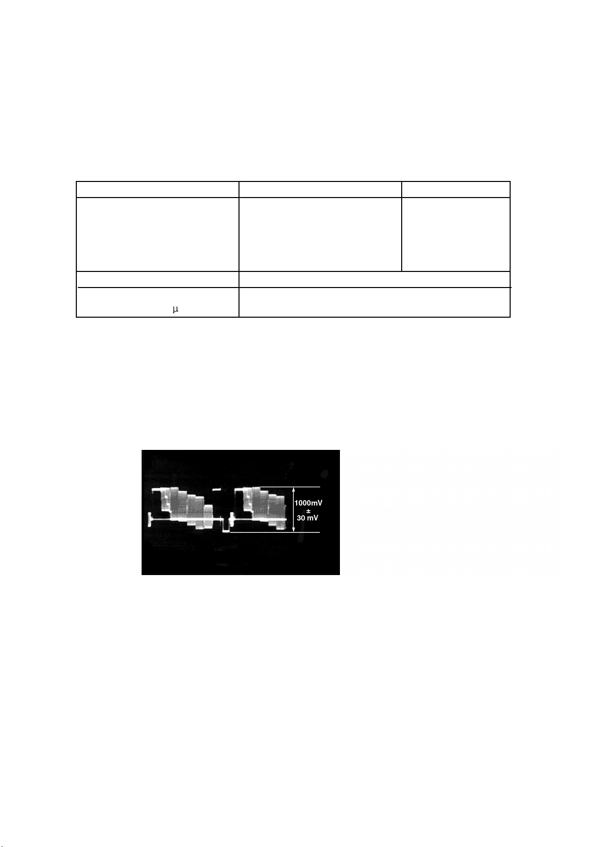
6.1. Video Output (Luminance Signal) Confirmation
6.Electrical Confirmation
6
DO this confirmation after replacing a P.C.B.
Measurement point
Video output terminal
Measuring equipment,tools
200mV/dir,10 sec/dir
Purpose:To maintain video signal output compatibility.
1.Connect the oscilloscope to the video output terminal and terminate at 75 ohms.
2.Confirm that luminance signal(Y+S)level is 1000mVp-p±30mV
PLAY(Title 46):DVDT-S15
PLAY(Title 12):DVDT-S01
Mode Disc
Color bar 75%
Confirmation value
1000mVp-p±30mV
DVDT-S15
or
DVDT-S01

Do the confirmation after replacing P.C.B.
Screwdriver,Oscilloscope
6.2 Video Output(Chrominance Signal) Confirmation
7
Measurement point
Video output terminal
Measuring equipment,tools Confirmation value
200mV/dir,10 sec/dir
Purpose:To maintain video signal output compatibility.
1.Connect the oscilloscope to the video output terminal and terminate at 75 ohme.
2.Confirm that the chrominance signal(C)level is 621 mVp-p±30mV
PLAY(Title 46):DVDT-S15
PLAY(Title 12):DVDT-S01
Mode Disc
Color bar 75%
621mVp-p±30mV
DVDT-S15
or
DVDT-S01
Audio
Scaling
interface
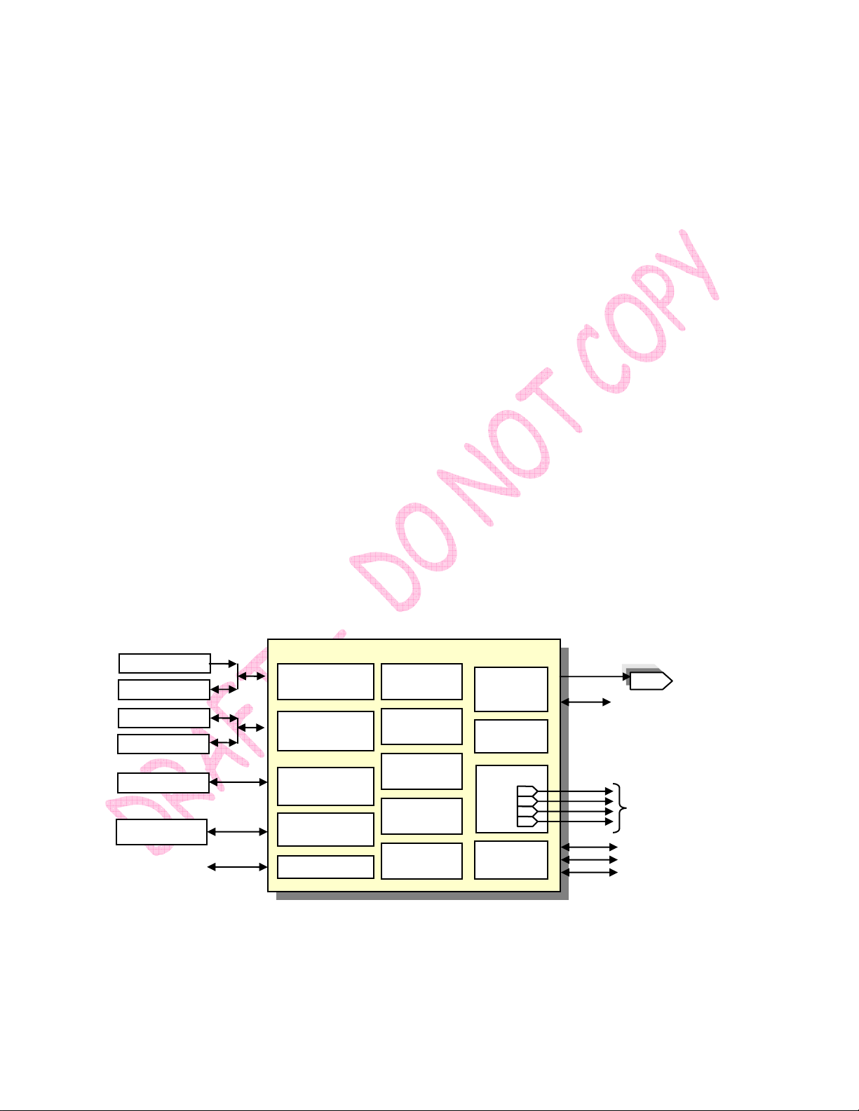
7. AML3298
1 Overview
The AML3298 A/V processor is a completely integrated system targeting all types of Audio/Video decoder
applications that provide connectivity to hard disk, digital camera, MP3 players and other external digital
consumer devices. The target market for AML3298 A/V processor is feature rich DVD players, audio receivers,
DVD/receiver combo players, digital media players, portable DVD players, and portable media players.
The AML3298 combines full function of MPEG-1, MPEG-2 and MPEG-4 decoding, numerous dedicated and
general-purpose peripherals, and a high speed 32-bit host CPU in a single device. The AML3298 has two built-in
AMRISC
The AML3298 also provides a high speed interface to external USB 1.1/2.0 chip for connectivity to popular USB
devices like hard disk, Flash memory, digital camera and MP3 players.
The embedded 32-bits host CPU handles system initialization, DVD navigation, and other system applications.
The AML3298 A/V processor provides a glueless interface to all external components: ATAPI loaders, USB
interface chip, audio DACs and memory. Numerous general-purpose I/O pins can be used to control the front
panel display and other miscellaneous tasks. The Flash interface allows the Flash memory to be shared with the
front-end chip to reduce system cost in mono-board designs. Together, the embedded host CPU and special
glueless interfaces reduce the total system cost for all A/V applications from any media.
The AML3298 A/V processor also integrates an NTSC/PAL TV encoder that supports S-Video, composite, YUV
component and RGB. The video encoder also supports high-quality de-interlaced progressive scan (480p/576p)
with full Macrovision support. Contrast enhancement, hue adjustment, video scaling, video interpolation, panscan, letter-box, and zoom are also supported. In addition, four built in video DACs complement the video
encoder further reducing system cost. In addition, the AML3288 devices can also provide CCIR601 and VGA
video output.
The integrated AMRISC
coded engine provides support for all existing audio formats and it also has enough flexibility to accommodate
new audio standards. Popular audio formats like Dolby AC-3 5.1, HDCD, MP-3 and WMA are supported. In
addition, SPDIF (IEC958) input and outputs are supported.
TM
RISC processors with special instructions to accommodate audio and video digital signal processing.
TM
RISC processor is designed to support advanced digital audio processing. The micro-
DVD-ROM
IDE HDD
FLASH
USB 1.1/2.0
SDRAM
JTAG
UART_RX
UART_TX
AML3298 A/V Processor
ATAPI / HDD
Flash Controller /
USB DMA Engine
DRAM Controller
32-bit CPU
UART
Amlogic, Inc.
Audio
AMRISC
Audio
Decoder
Audio/Video
Stream Praser
Video Decoder
Enhancement
Video
AMRISC
Figure 1 AML3298 Block Diagram
Audio
Interface
Video
& Conversion
Video
GPIO
ADATA
DACs
SPDIF (IEC958)
S-Video
CVBS
Component
Progressive
RGB
VD [7:0]
NGP[5:0]
IIS[7:0]
Company Confidential 8

2 Features
MPEG 1/2/4 Decoding
- MPEG-4 and Divx 3.x/4.x/5.x complaint
- MPEG-2 ML/MP conforming to ISO-13818
- MPEG-1 ML/MP conforming to ISO-11172
- On-chip CSS descrambler
- Flexible DRM engine for content management
- Compliant with DVD Specification 1.0 for read-only Disc
decoding
- Advanced error detection, concealment, and recovery
scheme
- Backward compatible VCD (1.0 - 2.0) decoding
- Super VCD decoding
- Built-in AMRISC
instruction extensions designed specifically for MPEG
decoding
TM
24-bit 133 MHz RISC CPU with special
Video
- Full MPEG-2 main profile @ main level 4:2:0 video
decoding
- Advanced pixel based de-interlacing algorithm
- On-Screen-Display (OSD) capable of supporting up to 256
prefixed colors or 16 programmable colors
- OSD Alpha-blending over video display
- Automatic scaling of sub-standard size DivX clips
- Video Zoom in for visual effects
- Built-in full screen NTSC to PAL scaling or vice-versa
- Built-in contrast enhancement and hue adjustment
- Built-in hardware for video interpolation and decimation
- Supports maximum zoom ratio up to 8X
Graphics
- Anti-flicker hardware for interlaced video
- Supports high speed block move for panning
- Built-in 2D graphics accelerator
- Dedicated graphics display controller separate from MPEG
engine for optimal video overlay performance
- Supports NTSC and PAL graphics modes with maximum
64K color
- Video overlay with graphics and vice-versa
- Unified MPEG and graphics memory architecture for
maximum flexibility and system cost savings
Built-in TV encoder
- Quad 10-bit video DACs
- Real-time Interlaced NTSC output 720x480 at 30 fps and
PAL 720x576 at 25 fps. Macrovision 7.1L1 anti-taping
process
- NTSC Progressive output (480p) at 60fps, PAL Progressive
(576p) at 50fps. Macrovision 1.03 anti-taping process
- Interlaced: S-Video, component, composite and SCART
output
- Close caption
Progressive RGB
-
Audio
- Built-in AMRISC
designed for Audio Processing
- Compliant with Dolby AC-3 5.1 channel decoding
- AC-3 two channel down-mixing
- SPDIF (IEC958) input and output
- Full MPEG audio layers I, II and III (MP3)
- Supports 8 channel linear PCM output
- DTS, HDCD, MP3 and WMA
TM
RISC CPU with extensions specifically
Built-in Host CPU
- 133Mhz 32-bit CPU dedicated for user applications
- Embedded debug interface using ICE/JTAG
- Able to utilize MPEG SDRAM as run time data storage for
minimal system cost
- Configurable for 16-bit wide SDRAM
- Support 8 or 16-bit FLASH
- FLASH memory can be shared with Front-End chips
Peripherals and Interface
- High speed (DMA) direct connection to third party USB chip
- Supports glueless interface to DVD DSP, CD DSP, and
DVD-ROM devices
- Direct connection to Audio DACs using I
- General Purpose I/O pins
- IDE with DMA transfer supporting up to 2 IDE devices such
as ATAPI DVD-ROM and IDE hard disk
- ISA interface
2
S
Miscellaneous
- 208-pin PQFP
- 1.8V operating voltage, 5V tolerant inputs, 3.3V output
Amlogic, Inc.
Company Confidential 9

AML3298 A/V Connectivity Processor
208 207 206 205 204 203 202 201 200 199 198 197 196 195 194 193 192 191 190 189 188 187 186 185 184 183 182 181 180 179 178 177 176 175 174 173 172 171 170 169 168 167 166 165 164 163 162 161 160 159 158 157
5354555657585960616263646566676869707172737475767778798081828384858687888990919293949596979899
100
101
102
103
04
AOCLK ADATA
ADATA
IEC
IIS
IIS
IIS
IIS
IIS
IIS
IIS
IIS
DD
VDD
VSS
VSS
VDD
DD
D
DMACK
DIOW
DIOR
CS
CS
DMARQ CSEL TDO RESET
TEST
TRST
TCK TDI T
AICLK
AICLK
SCLK
SCLK
DVDD
VSS
A
DVDD
DVSS
AVDD
AVSS
AVDD
AVSS
AVDD
AVSS
AVDD
AVSS
AVSS
AVDD
3 AML3298 – 208 Pin Package Diagram
ADATA_1
ADATA_0
ALRCLK
VSS_3.3V
AMCLK
VDD_3.3V
DD_13
DD_14
DD_15
DA_0
DA_1
DA_2
VSS_1.8V
VDD_1.8V
NGP_5
NGP_4
IVDD_DAC1 (1.8V)
VSS_DAC1 (1,8V)
IOX
_DAC1_X (3.3V)
_DAC1_X (3.3V)
IOB
_DAC1_B (3.3V)
-DAC1_B (3.3V)
IOG
-DAC1_G (3.3V)
-DAC1_G (3.3V)
IOR
_DAC1_R (3.3V)
_DAC1_R (3.3V)
COMP1
RSET1
VREF1_OUT
VREF1_IN
_DAC1 (3.3V)
_DAC1 (3.3V)
NGP_3
NGP_2
NGP_1
VDD_1.8V
VSS_1.8V
M2_CLKO
M2_DQM1
M2_BA1
M2_BA0
M2_SCS_N
VSS_3.3V
VDD_3.3V
UART_RX
UART_TX
NGP_0
VD_7
1
2
3
4
5
6
7
8
9
10
11
12
13
14
15
16
17
18
19
20
21
22
23
24
25
26
27
28
29
30
31
32
33
34
35
36
37
38
39
40
41
42
43
44
45
46
47
48
49
50
51
52
_2
_3
958
_0
_1
_6 VD_5 VD_4 VD_3 VD_2 VD_1 VD_0
VD
V
V
V
V
_3.3
_1.8
_3.3
_4
_5
_6
_7
_12 DD_11 DD_10 DD_9 DD_8 DD_7 DD_6 DD_5 DD_4
_2
_3
_1.8
AML3298
V
V
_3.3
_3.3
VDD
VSS
N
N
0
_
_
_5
_9
_11
A
A
A
RAS
CAS
2_
M
DQM
2_
2_
2_
2_
2_
M
M
M
M
M
V
N
V
_
_13
_8
_11
_12
_14
D
D
D
D
2_
2_
2_
2_
M
M
M
M
_10
_7
D
D
WE
2_
M
A
_3.3
_3.3
2_
2_
2_
VDD
M
M
M
VSS
_3
_9
D
2_
M
_2 DD_1 DD_0
D
_6
_8
A
A
2_
2_
M
M
N
_
N
V
_
ECS
_1.8
2_
VSS
M
T
1
1
N
N
_
N
_
0_
N
N
1_
_
N
N
_
_
XOUT
XIN
XOU
_
_
_
MS
0
XIN
_
0
1
PLL
PLL
PLL
PLL
_
_
_
_
PLL
_
VDD
AVSS_PLL0
156
AVDD_PLL0
155
VDD_3.3V
154
VSS_3.3V
153
M1_A_3
152
M1_A_2
151
M1_A_1
150
M1_A_0
149
M1_A_10
148
M1_A_11
147
M1_BA1
146
M1_BA0
145
M1_SCS_N
144
M1_RAS_N
143
M1_CAS_N
142
VDD_3.3V
141
VDD_1.8V
140
VSS_1.8V
139
DIORDY
138
IRQ14
137
VSS_3.3V
136
M2_D_15
135
M2_D_1
134
M2_D_2
133
M2_D_3
132
M2_D_4
131
M2_D_5
130
M2_D_6
129
M2_D_0
128
M2_D_7
127
M2_A_0
126
M2_A_1
125
M2_A_10
124
VDD_3.3V
123
VSS_3.3V
122
M2_A_2
121
M2_A_3
120
M2_A_4
119
M2_EOE_N
118
M1_EOE_N
117
M1_WE_N
116
M1_A_4
115
M1_A_5
114
M1_A_6
113
M1_A_7
112
M1_A_8
111
M1_A_9
110
VDD_1.8V
109
VSS_1.8V
108
M1_CLKO
107
VDD_3.3V
106
VSS_3.3V
105
1
N
V
_
_0
_1
_2
ECS
D
D
D
_1.8
1_
1_
1_
1_
VDD
M
M
M
M
V
V
_6
_7
_15
_14
_13
_3
_4
_5
D
1_
M
D
D
D
_3.3
_3.3
1_
1_
1_
VDD
M
VSS
M
M
_12
D
D
D
D
D
1_
1_
1_
1_
1_
M
M
M
M
M
1
_11
D
1_
M
0
_10
_9
_8
D
D
D
DQM
DQM
1_
1_
1_
1_
1_
M
M
M
M
M
Amlogic, Inc.
Company Confidential 10
A
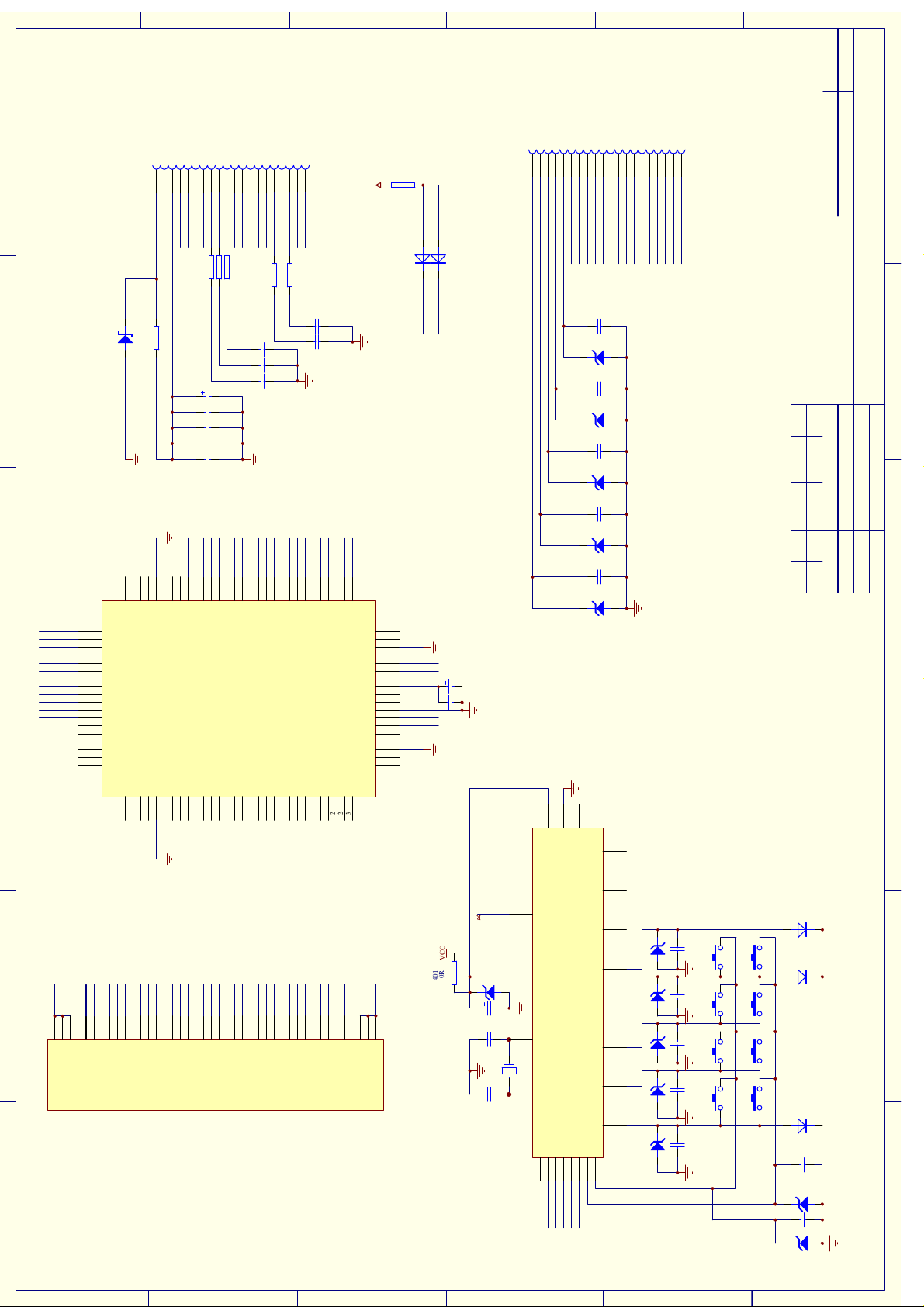
8. SCHEMATIC & PCB WIRING DIAGRAM SCHEMATIC & PCB WIRING DIAGRAM
FRONT SCHEMATIC DIAGRAM
11
B
C
D
E
F
1.0
6
XS403
XS19
19
IR
GND
+40V
FIL-
FIL+
VCC
R407
XS402
ZENER
10K
GND
100R
R405
VFD_CLK
100R
R406
VFD_STB
111214151613171820
100R
R404
VFD_DATA
GND
9107
VOL2-
VOL1-
5
TC402
100uF/100V
C408104
C407104
C406104
C405104
+40V+40V
SEG14
SEG15
SEG16
SEG17
SEG18
GRID1
GRID2
GRID3
GRID4
75
78
80
79
U402
PT6305
NC
NC
81
GRID5
GRID6
GRID7
GRID8
GRID9
GRID10
GRID11
GRID12
GRID13
GRID14
GRID15
GRID16
HVO24
82
HVO25
83
HVO26
84
HVO27
85
HVO28
86
HVO29
87
HVO30
88
HVO31
89
HVO32
90
HVO33
91
HVO34
92
HVO35
93
HVO36
94
HVO37
95
HVO38
96
HVO39
97
HVO40
98
HVO41
99
NC
100
NC1VDD22NC3NC4VSS25NC6NC7HOV428HOV439HOV4410HOV4511HOV4612HOV4713HOV4814NC15NC16NC17NC18NC19NC20NC21NC22NC23NC24NC25NC26NC27NC28NC29NC
VDD2
73
76
NC74NC
NC77NC
VSS2
CON4
VOL1+
VOL2+
R403100R
CON1
C402101
C401101
C423101
SEG10
SEG11
SEG12
SEG13
HVO1060HVO1161HVO1262HVO1363HVO1464HVO1565HVO1666HVO1767HVO1868HVO1969HVO2070HVO2171HVO2272HVO23
CON2
SEG9
59
2341568
CON3
R402100R
SEG8
GND
SEG7
C404
101
C403
101
SEG2
SEG3
SEG4
SEG5
SEG6
R408
4.7K
VCC
IR
1N4148
1N4148
VD404
VD403
VSDA-IR
IR#
SEG1
VDD2
HVO151HVO252HVO353HVO454HVO555HVO656HVO757HVO858HVO9
NC
NC
VSS2
NC
BK
PCB
LATB
VDD1
NC
NC
VSS1
CLKB
DI
NC
NC
VSS2
NC
NC
VDD2
30
+40V
50
49
48
47
46
45
CON2
44
CON1
TC403
VCC
VFD_STB
VFD_CLK
VFD_DATA
+40V
100uF/100V
C424
104
43
42
41
40
39
38
37
36
35
34
33
32
31
XS401
2341568
KX1
KX2
KX3
U401
SEL9VSS12CSS
9107
KX4
KX5K0K1K2K3K4VCC
22
111214151613171820
IR#
VOL1+
VOL2+
VOL2-
GND
47P
C415
ZD404
5.1V
47P
C414
ZD403
5.1V
47P
C413
ZD402
5.1V
47P
C412
ZD407
5.1V
47P
C416
ZD406
5.1V
HT6222
KEY7
14
XS20
19
第 1 张共 1 张 版次:
比例 质量 数量
BBK
VOL1-
CON3
CON4
GND
6
广东步步高电子工业有限公司AV厂
: 4S538SB
ABS538T
更改 数量 更改单号 签 名日期
主面板电路原理图
标准化
审 核
设 计
板号
5
批 准
REM
23 4
FIL+
GRID1
GRID2
GRID3
GRID4
GRID5
GRID6
GRID7
GRID8
42
38
F40F41F
VFD401
SEG18
GRID9
GRID10
GRID11
GRID12
GRID13
GRID14
GRID15
25
24
29
9G308G317G326G335G344G353G362G371G
P18
13G2612G2711G2810G
7
VSDA-IR
13
VCC
ZD401
3.3V
R401
100R
SEG1
SEG2
SEG3
SEG4
SEG5
SEG6
SEG7
SEG8
SEG9
SEG10
SEG11
SEG12
SEG13
SEG14
GRID16
21
16G2215G2314G
SEG15
12
P913P814P715P616P517P418P319P220P1
FIL-
SEG16
SEG17
TC401
3
F1F2F
P175P166P157P148P139P1210P1111P10
VFD-538
47uF/16V
8
C409
151
10
X401
455E
11
C410
151
KX023KX124KX21KX32KX43KX54KX65KX6
KX1
VDD
OSC0
OSC1
KX2
KEY6
15
/DREN
KEY5
16
C42247P
ZD413 5.1V
C421 47P
ZD412 5.1V
C420 47P
ZD411 5.1V
C419 47P
ZD410 5.1V
C418 47P
ZD409 5.1V
KX3
KX4
KX5
KEY4
17
KEY3
18
KEY2
19
KEY1
20
KEY0
21
6
KX7
KX6
1
A
B
C
D
E
VD405
SW1
SW1
SW1
SW1
1N4148
VD402
1N4148
VD401
1N4148
47P
C417
ZD408
5.1V
C41147P
K4
SW404
SW1
SW405
K3
SW403
SW1
SW408
K2
SW402
SW1
SW407
K1
SW401
SW1
SW406
K0
1234
ZD405
5.1V
F
 Loading...