


SERVICE MANUAL
bbk934S

CONTENTS
1. SAFETY PRECAUTIONS |
1 |
2.PREVENTION OF ELECTRO STATIC DISCHARGE(ESD)TO ELECTROSTATICALLY
|
SENSITIVE(ES)DEVICES |
1 |
3. |
CONTROL BUTTON LOCATIONS AND EXPLANATIONS |
2 |
4. |
PREVERTION OF STATIC ELECTRICITY DISCHARGE |
3 |
5. |
ASSEMBLING AND DISASSEMBLING THE MECHANISM UNIT |
4 |
5.1 |
OPTICAL PICKUP UNIT EXPLOSED VIEW AND PART LIST |
4 |
5.2 |
BRACKET EXPLOSED VIEW AND PART LIST |
6 |
5.3 |
MISCELLANEOUS |
7 |
6. |
ELECTRICAL CONFIRMATION |
8 |
6.1 |
VIDEO OUTPUT (LUMINANCE SIGNAL) CONFIRMATION |
8 |
6.2 |
VIDEO OUTPUT(CHROMINANCE SIGNAL) CONFIRMATION |
9 |
7. |
MPEG BOARD CHECK WAVEFORM |
10 |
8. |
IC BLOCK DIAGRAM & DESCRIPTION |
11 |
8.1 |
MT1336 |
11 |
8.2 |
MT1379 |
19 |
8.3 |
AM29LV160D |
35 |
8.4 |
HY57V641620HG |
40 |
9. |
SCHEMATIC & PCB WIRING DIAGRAM |
43 |
10. |
SPARE PARTS LIST |
57 |

1.1 GENERAL GUIDELINES
1.When servicing, observe the original lead dress. if a short circuit is found, replace all parts which have been overheated or damaged by the short circuit.
2.After servicing, see to it that all the protective devices such as insulation barrier, insulation papers shields are properly installed.
3.After servicing, make the following leakage current checks to prevent the customer from being exposed
to shock hazards.
Some semiconductor(solid state)devices can be damaged easily by static electricity. Such components commonly are called Electrostatically Sensitive(ES)Devices. Examples of typical ES devices are integrated circuits and some field-effect transistors and semiconductor chip components. The following techniques should be used to help reduce the incidence of component damage caused by electro static discharge(ESD).
1.Immediately before handling any semiconductor component or semiconductor-equipped assembly, drain off any ESD on your body by touching a known earth ground. Alternatively, obtain and wear a commercially availabel discharging ESD wrist strap, which should be removed for potential shock reasons prior to applying power to the unit under test.
2.After removing an electrical assembly equipped with ES devices,place the assembly on a conductive surface such as alminum foil, to prevent electrostatic charge buildup or exposure of the assembly.
3.Use only a grounded-tip soldering iron to solder or unsolder ES devices.
4.Use only an anti-static solder removal device. Some solder removal devices not classified as anti-static
(ESD protected)can generate electrical charge sufficient to damage ES devices.
5.Do not use freon-propelled chemicals. These can generate electrical charges sufficient to damage ES devices.
6.Do not remove a replacement ES device from its protective package until immediately before you are ready to install it. (Most replacement ES devices are packaged with leads electrically shorted together by conductive foam, alminum foil or comparable conductive material).
7.Immediately before removing the protective material from the leads of a replacement ES device, touch the protective material to the chassis or circuit assembly into which the device will be installed.
Caution
Be sure no power is applied to the chassis or circuit, and observe all other safety precautions.
8.Minimize bodily motions when handling unpackaged replacement ES devices. (Otherwise harmless motion such as the brushing together of your clothes fabric or the lifting of your foot from a carpeted floor can generate static electricity(ESD).
notice (1885x323x2 tiff)
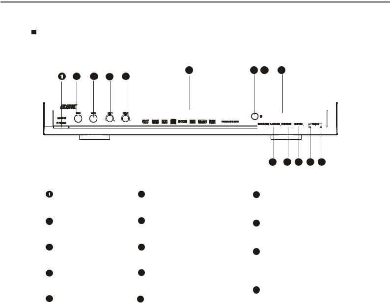
3.Control Button Locations and Explanations
Front Panel Illustration
6 |
7 |
8 |
9 |
2 |
3 |
4 |
5 |
|
|
|
|
|
|
|
|
|
|
|
|
|
|
|
|
|
|
|
|
|
|
|
|
|
|
|
|
|
|
|
|
|
|
|
|
|
|
|
|
|
|
|
|
|
|
|
|
|
|
|
|
|
|
|
|
|
|
|
|
|
|
|
|
|
|
|
|
|
|
|
|
|
|
|
|
|
|
|
|
|
|
|
|
|
|
|
|
|
|
|
|
|
|
|
|
|
|
|
|
|
|
|
|
|
|
|
|
|
|
|
|
|
|
|
|
|
|
|
|
|
|
|
|
|
|
|
|
|
|
|
|
|
|
|
|
|
|
|
|
|
|
|
|
|
|
|
|
|
|
|
|
|
|
|
|
|
|
|
|
|
|
|
|
|
|
|
|
|
|
|
|
|
|
|
|
|
|
|
|
|
|
|
|
|
|
|
|
|
|
|
|
|
|
|
|
|
|
|
10 11 12 13 14
|
POWER switch |
6 |
Disc tray |
2 |
MIC 1 jack |
7 |
Remote control signal sensor |
3 |
MIC 2 jack |
8 |
OPEN/CLOSE button |
4 |
MIC VOLUME 1 knob |
9 |
VFD display window |
5 |
MIC VOLUME 2 knob |
10 |
PLAY/PAUSE button |
11 STOP/BAND button
12FUNCTION button
13DVD MODE PREV button TUNER MODE TUNING button
14DVD MODE: NEXT button TUNER MODE: TUNING button
The laser diode in the traverse unit (optical pickup)may brake down due to static electricity of clothes or human body. Use due caution to electrostatic breakdown when servicing and handling the laser diode.
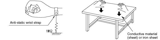
4.1.Grounding for electrostatic breakdown prevention
Some devices such as the DVD player use the optical pickup(laser diode)and the optical pickup will be damaged by static electricity in the working environment.Proceed servicing works under the working environment where grounding works is completed.
4.1.1. Worktable grounding
1.Put a conductive material(sheet)or iron sheet on the area where the optical pickup is placed,and ground the sheet.
4.1.2.Human body grounding
1 Use the anti-static wrist strap to discharge the static electricity from your body.
safety_3 (1577x409x2 tiff)
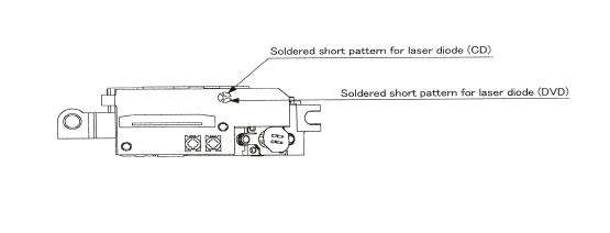
4.1.3.Handling of optical pickup
1.To keep the good quality of the optical pickup maintenance parts during transportation and before installation, the both ends of the laser diode are short-circuited.After replacing the parts with new ones, remove the short circuit according to the correct procedure. (See this Technical Guide).
2.Do not use a tester to check the laser diode for the optical pickup .Failure to do so willdamage the laser diode due to the power supply in the tester.
4.2. Handling precautions for Traverse Unit (Optical Pickup)
1.Do not give a considerable shock to the traverse unit(optical pickup)as it has an extremely high-precise structure.
2.When replacing the optical pickup, install the flexible cable and cut is short land with a nipper. See the optical pickup replacement procedure in this Technical Guide. Before replacing the traverse unit, remove the short pin for preventingstatic electricity and install a new unit.Connect the connector as short times as possible.
3.The flexible cable may be cut off if an excessive force is applied to it.Use caution when handling the cable
4.The half-fixed resistor for laser power adjustment cannot be adjusted. Do not turn the resistor.

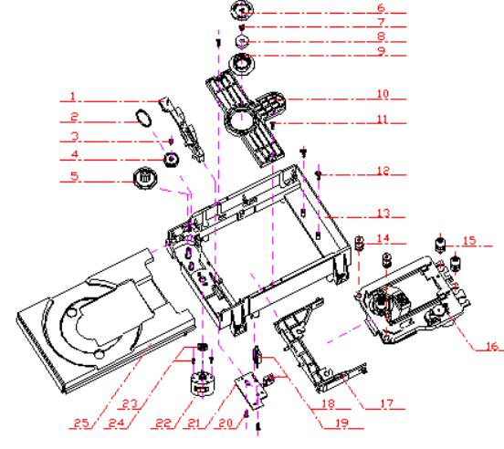
5.1 Optical pickup Unit Explosed View and Part List
Pic (1)

Materials to Pic (1)
No. |
PARTS CODE |
PARTS NAME |
Q ty |
|
|
|
|
|
14692200 |
SF-HD60 |
1 |
1 |
1EA0311A06300 |
ASSY, CHASSIS, COMPLETE |
1 |
2 |
1EA0M10A15500 |
ASSY, MOTOR, SLED |
1 |
Or |
1EA0M10A15501 |
ASSY, MOTOR, SLED |
1 |
3 |
1EA2451A24700 |
HOLDER, SHAFT |
3 |
4 |
1EA2511A29100 |
GEAR, RACK |
1 |
5 |
1EA2511A29200 |
GEAR, DRIVE |
1 |
6 |
1EA2511A29300 |
GEAR, MIDDLE, A |
1 |
7 |
1EA2511A29400 |
GEAR, MIDDLE, B |
1 |
8 |
1EA2744A03000 |
SHAFT, SLIDE |
1 |
9 |
1EA2744A03100 |
SHAFT, SLIDE, SUB |
1 |
10 |
1EA2812A15300 |
SPRING, COMP, TYOUSEI |
3 |
11 |
1EA2812A15400 |
SPRING, COMP, RACK |
1 |
|
|
|
|
21 |
1EA0B10B20100 |
ASSY, PWB |
1 |
Or |
1EA0B10B20200 |
ASSY, PWB |
1 |
|
|
|
|
31 |
SEXEA25700--- |
SPECIAL SCREW BIN+-M2X11 |
3 |
32 |
SEXEA25900--- |
SPECIAL SCREW M1.7X2.2 |
2 |
33 |
SFBPN204R0SE- |
SCR S-TPG PAN 2X4 |
2 |
34 |
SFSFN266R0SE- |
SCR S-TPG FLT 2.6X6 |
1 |
35 |
SWXEA15400--- |
SPECIAL WASHER 1.8X4 X0.25 |
2 |
Note : This parts list is not for service parts supply.
5.2 Bracket Explosed View and Part List
Materials to Pic(2) |
Pic (2) |
|
|
||
1.bracket |
14. front silicon rubber |
|
2.belt |
15. Back silicon rubber |
|
3.screw |
16. Pick-up |
|
4.belt wheel |
17. Pick-up |
|
5.gearwheel |
18. switch |
|
6.iron chip |
19. Five-pin flat plug |
|
7. |
Immobility mechanism equipment |
20. screw |
8. Magnet |
21. PCB |
|
9. |
Platen |
22. motor |
10. |
Bridge bracket |
23. Motor wheel |
11. screw |
24. screw |
|
12. screw |
25.tray |
|
13. |
Big bracket |
|
Before going process with disassembly and installation, please carefully both peruse the chart and confirm the materials.
5.3 MISCELLANEOUS
5.3.1 Protection of the LD(Laser diode)
Short the parts of LD circuit pattern by soldering.
5.3.2 Cautions on assembly and adjustment
Make sure that the workbenches,jigs,tips,tips of soldering irons and measuring instruments are grounded,and that personnel wear wrist straps for ground.
Open the LD short lands quickly with a soldering iron after a circuit is connected.
Keep the power source of the pick-up protected from internal and external sources of electrical
noise.
Refrain from operation and storage in atmospheres containing corrosive gases (such as H2S,SO2, NO2 and Cl2)or toxic gases or in locations containing substances(especially from the organic silicon,cyan, formalin and phenol groups)which emit toxic gases.It is particularly important to ensure that none of the above substances are present inside the unit.Otherwise,the motor may no longer run.
6.1. Video Output (Luminance Signal) Confirmation |
|
|
DO this confirmation after replacing a P.C.B. |
|
|
Measurement point |
Mode |
Disc |
|
Color bar 75% |
DVDT-S15 |
Video output terminal |
PLAY(Title 46):DVDT-S15 |
or |
|
PLAY(Title 12):DVDT-S01 |
DVDT-S01 |
Measuring equipment,tools |
Confirmation value |
|
200mV/dir,10 sec/dir |
1000mVp-p±30mV |
|
Purpose:To maintain video signal output compatibility.
1.Connect the oscilloscope to the video output terminal and terminate at 75 ohms. 2.Confirm that luminance signal(Y+S)level is 1000mVp-p±30mV
Do the confirmation after replacing P.C.B. |
|
|
Measurement point |
Mode |
Disc |
|
Color bar 75% |
DVDT-S15 |
Video output terminal |
PLAY(Title 46):DVDT-S15 |
or |
|
PLAY(Title 12):DVDT-S01 |
DVDT-S01 |
Measuring equipment,tools |
Confirmation value |
|
Screwdriver,Oscilloscope |
|
|
200mV/dir,10 sec/dir |
621mVp-p±30mV |
|
Purpose:To maintain video signal output compatibility.
1.Connect the oscilloscope to the video output terminal and terminate at 75 ohme.
2.Confirm that the chrominance signal(C)level is 621 mVp-p±30mV


MT1336
PRELIMINARY, SUBJ ECT TO CHANGE WITHOUT NOTICE |
MTK CONFIDENTIAL, NO DISCLOSURE |
GENERAL DESCRIPTION
M T 1 3 3 6 i s a h i g h p e r f o r m a n c e C M O S a n a l o g f r o n t -e n d I C f o r b o t h C D _ R O M d r i v e r u p t o 4 8 X S a n d
D V D - R O M d r i v e r u p t o 1 6 X S . I t a l s o s u p p o r t s D V D- R A M r e a d u p t o 4 X S V e r s i o n 2 . I t c o n t a i n s s e r v o a m p lifiers
t o g e n e r a t e f o c u s i n g e r r o r , 3-b e a m t r a c k i n g e r r o r , 1 b e a m r a d i a l p u s h -p u l l s i g n a l , R F l e v e l a n d S B A D f o r s e r v o f u n c t i o n s . I t a l s o i n c l u d e s D P D t r a c k i n g e r r o r s i g n a l f o r D V D _ R O M a p p l i c a t i o n . F o r D V D- R A M d i s k s , t h e r e a r e also Differential Push -P u l l ( D P P ) m e t h o d f o r g e n e r a t i n g t r a c k i n g s i g n a l a n d D i f f e r e n t i a l A s t i g m a t i c D e t e c t i o n ( D A D ) f o r p r o c e s s i n g f o c u s i n g s i g n a l . P r o g r a m m a b l e e q u a l i z e r a n d A G C c i r c u i t s a r e a l s o i n c o r p o r a t e d i n t h i s c h i p t o o p t i m i z e r e a d c h a n n e l p e r f o r m a n c e . I n a d d i t i o n , t h i s c h i p h a s d u a l a u t o m a t i c l a s e r p o w e r c o n t r o l c i r c u i t s f o r D V D- R O M ( D V D-R A M ) a n d C D -R O M s e p e r a t e l y a n d r e f e r e n c e v o l t a g e g e n e r a t o r s t o r e d u c e e x t e r n a l c o m p o n e n t s . P r o g r a m m a b l e f u n c t i o n s a r e i m p l e m e n t e d b y t h e a c c e s s o f i n t e r n a l r e g i s t e r t h r o u g h b i -d i r e c t i o n a l serial port to configure modes selection.
FEATURES
n |
R F e q u a l i z e r w i t h p r o g r a m m a b l e f c f r o m 3 M H z t o 7 0 M H z a n d p r o g r a m m a b l e b o o s t f r o m 3 d B t o |
|
13dB. |
n |
M T 1 3 3 6 s u p p o r t s a t l e a s t e i g h t d i f f e r e n t k i n d s o f p i c k-u p h e a d s w i t h v e r s a t i l e i n p u t c o n f i g u r ation for |
|
both RF input stages and servo signal blocks. |
nVersatile on -line AGC.
n3 beams tracking error signal generator for CD_ROM application.
nOne beam differential phase tracking error (DPD) generator for DVD_ROM application.
nDifferential push pull tracki ng error (DPP) generator for DVD_RAM application.
nFocusing error signal generator for CD-ROM, DVD-ROM and DVD-RAM (DAD method).
nRF level signal generator.
nSub-beam added signal for 3 beams CD_ROM.
nOne beam push -pull signal generator for central servo application.
nHigh speed RF envelop detection circuit with bandwidth up to 400KHz for CD-ROM.
nDefect and Blank detection circuits.
nDual automatic laser power control circuits with programmable level of LD monitor voltage.
nVref=1.4V voltage and V2ref=2.8V voltage generators.
nV20=2.0V voltage for pick -up head reference.
nBi-directional serial port to access internal registers.
MT1336
PRELIMINARY, SUBJ ECT TO CHANGE WITHOUT NOTICE |
MTK CONFIDENTIAL, NO DISCLOSURE |
||
|
|
|
|
DVDA 
CDA
DVDB 
CDB
DVDC 
CDC
DVDD 
CDD  DVDRFIN
DVDRFIP MA  MB
MB  MC
MC  MD
MD  SA
SA  SB
SB  SC
SC
SD
DPFN 
DPFO 
IR
DPDMUTE
TPI
TNI
CDFOP
CDFON
RFGC
RFGCU
RFGCI 
AGC1
AGC2
AGC3
RFSUBO
WOBSO 
V20
V2REFO 
VREFO
ATTENUATORINPUTMUX
WOBBLE
DET
VGA |
|
|
|
EQ |
|
|
|||||
|
|
|
|
|
|
|
|
|
|
|
|
|
|
|
|
|
|
ENVELOP
DETECTOR
AGC
DPD
|
|
PCS |
SBAD |
|
|
|
|
|
|
|
|
TE |
|
|
|
DVD |
|
|
|
|
|
|
APC |
|
||
|
|
|
RF
LEVEL
|
|
|
FE |
|
CD |
|
|
|
|
|
APC |
|
|
|
|
|
|
CENTRAL
SERVO
SERIAL
PORT
REF and 2VREF
Voltage Generator
OSP
OSN
RFOP
RFON
LRFRP
DEFECT
HRFRP
CRTP CRTPLP
CSO
LVL
TEO
FEO
REFCOS HALLCOS COSPHI REFSIN HALLSIN SINPHI
MDI2
LDO2
MDI1
LDO1
UDGATE IDGATE VFO13
SDATA
SLCK
SDEN
MT1336 FUNCTION BLOCKS DIAGRAM

|
MT1336 |
PRELIMINARY, SUBJ ECT TO CHANGE WITHOUT NOTICE |
MTK CONFIDENTIAL, NO DISCLOSURE |
WOBSO |
|
|
|
1 |
|
|
|
|
|
WVDD |
|
2 |
||
AGNDX |
|
3 |
||
AGNDX |
|
|
4 |
|
AVDDO |
|
5 |
||
RFOP |
|
|
6 |
|
|
|
|
|
|
RFON |
|
7 |
||
AGNDO |
|
|
|
8 |
|
|
|||
TM1 |
|
|
9 |
|
|
|
|||
TM2 |
|
10 |
||
|
|
|
||
TM3 |
|
|
11 |
|
AGNDT |
|
12 |
||
|
|
|
||
TM4 |
|
13 |
||
AVDDT |
|
|
14 |
|
|
|
|
|
|
V2REFO |
|
15 |
||
VREFO |
|
16 |
||
V20 |
|
17 |
||
FEO |
|
18 |
||
LVL |
|
19 |
||
|
|
|
|
|
CSO |
|
20 |
||
|
|
|
||
TEO |
|
21 |
||
|
||||
VDDP |
|
22 |
||
|
||||
DEFECT |
|
23 |
||
|
||||
LRFRP |
|
24 |
||
|
||||
HRFRP |
|
25 |
||
|
||||
CRTP |
|
26 |
||
CRTPLP |
|
|
27 |
|
|
|
|
|
|
TRLPA |
|
28 |
||
TRLP |
|
29 |
||
HTRC |
|
30 |
||
GNDP |
|
31 |
||
DPFN |
|
32 |
||
DPFO |
|
33 |
||
|
||||
AGNDX |
|
34 |
||
|
||||
AGNDX |
|
35 |
||
|
||||
AGNDX |
|
36 |
||
|
||||
VDD |
|
37 |
||
|
||||
VFO13 |
|
38 |
||
WGND |
RFSUBO |
LDO2 |
LDO1 |
MDI1 |
MDI2 |
AGC3 |
AGC2 |
WAVDD |
AGC1 |
WAGND |
SGND |
|
TNI |
TPI |
SVDD |
CDFON |
CDFOP |
SD |
SC |
AVDD |
IR |
AGND |
SB |
SA |
MD |
MC |
||||||||||||||||||||||||||||||||||||
|
|
|
|
|
|
|
|
|
|
|
|
|
|
|
|
|
|
|
|
|
|
|
|
|
|
|
|
|
|
|
|
|
|
|
|
|
|
|
|
|
|
|
|
|
|
|
|
|
|
|
|
|
|
|
|
|
|
|
|
|
|
|
|
|
|
|
|
|
|
|
|
|
|
|
|
|
|
|
|
|
|
|
|
|
|
|
|
|
|
|
|
|
|
|
|
|
|
|
|
|
|
|
|
|
|
|
|
|
|
|
|
|
|
|
|
|
|
|
|
|
|
|
|
|
|
128 |
127 |
126 |
|
125 |
|
124 |
123 |
|
122 |
121 |
120 |
|
119 |
118 |
117 |
116 |
115 |
114 |
113 |
112 |
|
111 |
110 |
109 |
108 |
107 |
106 |
105 |
104 |
103 |
||||||||||||||||||||||||||||||||
MT1336
DVD-ROM
With
DVD_RAM
Read
39 |
40 |
41 |
|
42 |
|
43 |
|
44 |
|
45 |
46 |
|
47 |
|
48 |
|
49 |
|
50 |
51 |
52 |
53 |
54 |
55 |
|
56 |
57 |
58 |
59 |
|
60 |
|
61 |
62 |
63 |
64 |
||||||||||||||||||||||||||||
|
|
|
|
|
|
|
|
|
|
|
|
|
|
|
|
|
|
|
|
|
|
|
|
|
|
|
|
|
|
|
|
|
|
|
|
|
|
|
|
|
|
|
|
|
|
|
|
|
|
|
|
|
|
|
|
|
|
|
|
|
|
|
|
|
|
|
|
|
|
|
|
|
|
|
|
|
|
|
|
|
|
|
|
|
|
|
|
|
|
|
|
|
|
|
|
|
|
|
|
|
|
|
|
|
|
|
|
|
|
|
|
|
|
|
|
|
|
|
|
|
|
|
|
|
|
|
|
|
|
GND |
UDGATE |
HDGATE |
IO0 |
IO1 |
IO2 |
IO3 |
IO4 |
IO5 |
IO6 |
IO7 |
IO8 |
IO9 |
IOA IOB |
VDDS |
XCK16M |
SCLK |
GNDS SDEN |
SDATA |
RST |
DPDMUTE |
AGNDP |
AGNDX |
AVDDP |
|||||||||||||||||||||||||||||||||||||||||
102  MB
MB
101  MA
MA
100  DVDA
DVDA
99  DVDB
DVDB
98  DVDC
DVDC
97  DVDD
DVDD
96  DVDRFIP
95  DVDRFIN
94  CDA
CDA
93  CDB
CDB
92  CDC
CDC
91  CDD
CDD
90  OSN
OSN
89  OSP
OSP
88  RFGC
RFGC
87  RFGCU
RFGCU
86  RFGCI
RFGCI
85  CEQP
CEQP
84  CEQN
CEQN
83  AGNDX
AGNDX
82  AGNDX
AGNDX
81  MON
MON
80  MOP
MOP
79  SW1
SW1
78  SW2
SW2
77  SWO
SWO
76  SINPHI
75  REFSIN
74  HALLSIN
73  AGNDM
AGNDM
72  REFCOS
71  HALLCOS
70  COSPHI
69  AVDDM
AVDDM
68  AGNDX
AGNDX
67  AVDDF
AVDDF
66  VCON
VCON
65  AGNDF
AGNDF
MT1336 PIN ASSIGNMENT

|
|
|
|
|
|
|
MT1336 |
|
PRELIMINARY, SUBJ ECT TO CHANGE WITHOUT NOTICE |
|
MTK CONFIDENTIAL, NO DISCLOSURE |
||||||
|
|
|
|
|
MT1336 PIN DESCRIPTIONS |
|
|
|
|
|
|
|
|
|
|
||
Pin Numbers |
|
|
Symbol |
Type |
Description |
|
||
|
|
|
|
|
|
|
|
|
|
|
|
|
|
|
|
|
|
LQFP128 |
|
|
|
|
|
|
||
|
|
|
|
|
|
|
|
|
RF Flag Interface |
|
|
|
|
|
|
||
|
|
|
|
|
|
|
|
|
23 |
|
|
DEFECT |
Digital Output |
Flag of bad data output status |
|
|
|
|
|
|
|
|
|
|
|
|
RF SIO interface |
|
|
|
|
|
|
||
|
|
|
|
|
|
|
|
|
56 |
|
|
SCLK |
Digital Input |
RF serial clock input |
|
|
|
|
|
|
|
|
|
|
|
|
58 |
|
|
SDEN |
Digital Input |
RF serial data enable |
|
|
|
|
|
|
|
|
|
|
|
|
59 |
|
|
SDATA |
Digital IO |
RF serial data IO |
|
|
|
60 |
|
|
RST |
Digital input |
Reset (active high) |
|
|
|
|
|
|
|
|
|
|
|
|
55 |
|
|
XCK16M |
Digital Input |
16.9MHz for verification |
|
|
|
|
|
|
|
|
|
|
|
|
RF SERVO interface |
|
|
|
|
|
|
||
|
|
|
|
|
|
|
|
|
40 |
|
|
UDGATE |
Digital |
Input |
Con trol signal for DVD-RAM |
|
|
|
|
|
|
|
|
|
|
|
41 |
|
|
IDGATE |
Digital |
Input |
Control signal for DVD -RAM |
|
|
|
|
|
|
|
|
|
|
|
38 |
|
|
VFO13 |
Digital |
Input |
DVD -RAM Header signal |
|
|
|
|
|
|
|
|
|
|
|
RF |
|
|
|
|
|
|
||
|
|
|
|
|
|
|
|
|
100 |
|
|
DVDA |
Analog input |
AC coupled DVD RF signal input |
A |
|
|
|
|
|
|
|
|
|
|
|
99 |
|
|
DVDB |
Analog Input |
AC coupled DVD RF signal input |
B |
|
|
|
|
|
|
|
|
|
|
|
98 |
|
|
DVDC |
Analog Input |
AC coupled DVD RF signal input |
C |
|
|
|
|
|
|
|
|
|
|
|
97 |
|
|
DVDD |
Analog Input |
AC coupled DVD RF signal input |
D |
|
|
|
|
|
|
|
|
|
|
|
95 |
|
|
DVDRFIN |
Analog Input |
AC coupled DVD RF signal input |
RFIN |
|
|
|
|
|
|
|
|
|
|
|
96 |
|
|
DVDRFIP |
Analog Input |
AC coupled DVD RF signal input |
RFIP |
|
|
|
|
|
|
|
|
|
|
|
94 |
|
|
CDA |
Analog Input |
AC coupled CD RF signal input |
A |
|
|
|
|
|
|
|
|
|
|
|
93 |
|
|
CDB |
Analog Input |
AC coupled CD RF signal input |
B |
|
|
|
|
|
|
|
|
|
|
|
92 |
|
|
CDC |
Analog Input |
AC coupled CD RF signal input |
C |
|
|
|
|
|
|
|
|
|
|
|
91 |
|
|
CDD |
Analog Input |
AC coupled CD RF signal input |
D |
|
|
|
|
|
|
|
|
|
||
90 |
|
|
OSN |
Analog |
RF Offset cancellation capacitor connecting |
|
||
|
|
|
|
|
|
|
||
89 |
|
|
OSP |
Analog |
RF Offset cancellation capacitor connecting |
|
||
|
|
|
|
|
|
|
||
85 |
|
|
CEQP |
Analog |
RF Offset cancellation capacitor connecting |
|
||
|
|
|
|
|
|
|
||
84 |
|
|
CEQN |
Analog |
RF Offset cancellation capacitor connecting |
|
||
|
|
|
|
|
|
|
||
88 |
|
|
RFGC |
Analog |
RF AGC loop capacitor connecting for DVD -ROM |
|
||
|
|
|
|
|
|
|
|
|

|
|
|
|
|
|
MT1336 |
|
PRELIMINARY, SUBJ ECT TO CHANGE WITHOUT NOTICE |
MTK CONFIDENTIAL, NO DISCLOSURE |
||||||
|
|
|
|
|
|
|
|
87 |
|
RFGCU |
|
Analog |
RF AGC loop capacitor connecting for DVD -RAM |
|
|
|
|
|
|
|
|
|
|
86 |
|
RFGCI |
|
Analog |
RF AGC loop capacitor connecting for DVD -RAM |
|
|
|
|
|
|
|
|
|
|
101 |
|
MA |
|
Analog Input |
DC coupled DVD-RAM main-beam RF signal input |
A |
|
|
|
|
|
|
|
|
|
102 |
|
MB |
|
Analog Input |
DC coupled DVD-RAM main-beam RF signal input |
B |
|
|
|
|
|
|
|
|
|
103 |
|
MC |
|
Analog Input |
DC coupled DVD-RAM main-beam RF signal input |
C |
|
|
|
|
|
|
|
|
|
104 |
|
MD |
|
Analog Input |
DC coupled DVD-RAM main-beam RF signal input |
D |
|
|
|
|
|
|
|
|
|
105 |
|
SA |
|
Analog Input |
DC coupled DVD-RAM sub-beam RF signal input |
A |
|
|
|
|
|
|
|
|
|
106 |
|
SB |
|
Analog Input |
DC coupled DVD-RAM sub-beam RF signal input |
B |
|
|
|
|
|
|
|
|
|
110 |
|
SC |
|
Analog Input |
DC coupled DVD-RAM sub-beam RF signal input |
C |
|
|
|
|
|
|
|
|
|
111 |
|
SD |
|
Analog Input |
DC coupled DVD-RAM sub-beam RF signal input |
D |
|
|
|
|
|
|
|
|
|
108 |
|
IR |
|
Analog |
External current bias resistor (R=20K) |
|
|
|
|
|
|
|
|
|
|
119 |
|
AGC1 |
|
Analog |
Wobble AGC loop1 capacitor |
|
|
|
|
|
|
|
|
|
|
121 |
|
AGC2 |
|
Analog |
Wobble AGC loop2 capacitor |
|
|
|
|
|
|
|
|
|
|
122 |
|
AGC3 |
|
Analog |
Wobble AGC loop3 capacitor |
|
|
|
|
|
|
|
|
|
|
127 |
|
RFSUBO |
|
Analog output |
Header push-pull RF output signal |
|
|
|
|
|
|
|
|
|
|
1 |
|
WOBSO |
|
Digital output |
Wobble signal output |
|
|
|
|
|
|
|
|
|
|
6 |
|
RFOP |
|
Analog output |
RF positive output |
|
|
|
|
|
|
|
|
|
|
7 |
|
RFON |
|
Analog output |
RF negative output |
|
|
|
|
|
|
|
|
|
|
TRACKING ERROR |
|
|
|
|
|
|
|
|
|
|
|
|
|
|
|
32 |
|
DPFN |
|
Analog |
DPD amplifier negative input |
|
|
|
|
|
|
|
|
|
|
33 |
|
DPFO |
|
Analog |
DPD amplifier output |
|
|
|
|
|
|
|
|
|
|
61 |
|
DPDMUTE |
|
Digital input |
DPD mute control input |
|
|
|
|
|
|
|
|
|
|
116 |
|
TNI |
|
Analog Input |
3 beam satellite PD signal negative input |
|
|
|
|
|
|
|
|
|
|
115 |
|
TPI |
|
Analog Input |
3 beam satellite PD signal positive input |
|
|
|
|
|
|
|
|
|
|
21 |
|
TEO |
|
Analog Output |
Tracking error output |
|
|
|
|
|
|
|
|
|
|
FOCUSING ERROR & RF LEVEL |
& CENTRAL SERVO SIGNAL |
|
|
||||
|
|
|
|
|
|
|
|
112 |
|
CDFOP |
|
Analog Input |
CD focusing error positive input |
|
|
|
|
|
|
|
|
|
|
113 |
|
CDFON |
|
Analog Input |
CD focusing error negative input |
|
|
|
|
|
|
|
|
|
|
18 |
|
FEO |
|
Analog Output |
Focusing error output |
|
|
|
|
|
|
|
|
|
|
19 |
|
LVL |
|
Analog Output |
RF level output |
|
|
|
|
|
|
|
|
|
|
20 |
|
CSO |
|
Analog output |
Central servo signal output |
|
|
|
|
|
|
|
|
|
|
ALPC |
|
|
|
|
|
|
|
|
|
|
|
|
|
|
|

|
|
|
MT1336 |
|
PRELIMINARY, SUBJ ECT TO CHANGE WITHOUT NOTICE |
MTK CONFIDENTIAL, NO DISCLOSURE |
|||
|
|
|
|
|
124 |
MDI1 |
Analog Input |
Laser power monitor input |
|
|
|
|||
|
|
|
|
|
125 |
LDO1 |
Analog Ou tput |
Laser driver output |
|
|
|
|
|
|
123 |
MDI2 |
Analog Input |
Laser power monitor input |
|
|
|
|
|
|
126 |
LDO2 |
Analog Output |
Laser driver output |
|
|
|
|
|
|
RFRIPPLE |
|
|
|
|
|
|
|
|
|
26 |
CRTP |
Analog |
RF top envelop filter capacitor connecting |
|
|
|
|
|
|
27 |
CRTPLP |
Analog |
Defect level filter capacitor connecting |
|
|
|
|
|
|
25 |
HRFRP |
Analog output |
High frequency RF ripple output or Blank detector’s output |
|
|
|
|
|
|
24 |
LRFRP |
Analog output |
Low frequency RF ripple output |
|
|
|
|
|
|
POWER |
|
|
|
|
|
|
|
|
|
67, 69 |
AVDD |
Power |
Master PLL Filter power |
|
|
|
|
|
|
65, 73 |
AGND |
GND |
GND for Master PLL Filter |
|
|
|
|
|
|
64 |
AVDD |
Power |
DPD Power |
|
|
|
|
|
|
62 |
AGND |
GND |
DPD GND |
|
|
|
|
|
|
109 |
AVDD |
Power |
RF path Power |
|
|
|
|
|
|
107 |
AGND |
GND |
RF path GND |
|
|
|
|
|
|
114 |
SVDD |
Power |
Servo Power |
|
|
|
|
|
|
117 |
SGND |
GND |
Servo GND |
|
|
|
|
|
|
2,120 |
WAVDD |
Power |
Wobble Power |
|
|
|
|
|
|
128,118 |
WAGND |
GND |
Wobble GND |
|
|
|
|
|
|
5 |
AVDDO |
Power |
Power for RF output |
|
|
|
|
|
|
8 |
AGNDO |
GND |
GND for RF output |
|
|
|
|
|
|
14 |
AVDDT |
Power |
Power for Trimming PAD |
|
|
|
|
|
|
12 |
AGNDT |
GND |
GND for Trimming PAD |
|
|
|
|
|
|
22 |
VDDP |
Power |
Peak Detection Power |
|
|
|
|
|
|
31 |
GNDP |
GND |
Peak Detection GND |
|
|
|
|
|
|
37,54 |
VDD |
Power |
Serial I/O Power |
|
|
|
|
|
|
39,57 |
GND |
GND |
Serial I/O GND |
|
|
|
|
|
|
REFERENCE VOLTAGE |
|
|
|
|
|
|
|
|
|
16 |
VREFO |
Analog output |
Reference voltage 1.4V |
|
|
|
|
|
|
15 |
V2REFO |
Analog output |
Reference voltage 2.8V |
|
|
|
|
|
|
17 |
V20 |
Analog Output |
Reference voltage 2.0V |
|
|
|
|
|
|

|
|
|
|
|
MT1336 |
|
PRELIMINARY, SUBJ ECT TO CHANGE WITHOUT NOTICE |
MTK CONFIDENTIAL, NO DISCLOSURE |
|||||
|
|
|
|
|
|
|
ALPC TRIMMING |
|
|
|
|
|
|
|
|
|
|
|
|
|
9 |
|
TM1 |
Analog input |
Trimming pin for ALPC1 |
|
|
|
|
|
|
|
|
|
10 |
|
TM2 |
Analog input |
Trimming pin for ALPC1 |
|
|
|
|
|
|
|
|
|
11 |
|
TM3 |
Analog input |
Trimming pin for ALPC2 |
|
|
|
|
|
|
|
|
|
13 |
|
TM4 |
Analog input |
Trimming pin for ALPC2 |
|
|
|
|
|
|
|
|
|
HIGH SPEED TRACK COUNTING |
|
|
|
|
||
|
|
|
|
|
|
|
29 |
|
TRLP |
Analog |
Low-pass filter capacitor connecting |
|
|
|
|
|
|
|
|
|
28 |
|
TRLPA |
Analog |
Low-pass filter capacitor connecting |
|
|
|
|
|
|
|
|
|
30 |
|
HTRC |
Digital output |
High speed track counting digital output |
|
|
|
|
|
|
|
|
|
PCS |
|
|
|
|
|
|
|
|
|
|
|
|
|
74 |
|
HALLSIN |
Analog input |
Negative input of amplifier for hall sensor signal |
|
|
|
|
|
|
|
|
|
75 |
|
REFSIN |
Analog input |
Positive input of amplifier for hall sensor signal |
|
|
|
|
|
|
|
|
|
76 |
|
SINPHI |
Analog output |
Amplifier output for hall sensor signal |
|
|
|
|
|
|
|
|
|
71 |
|
HALLCOS |
Analog input |
Negative input of amplifier for hall sensor signal |
|
|
|
|
|
|
|
|
|
72 |
|
REFCOS |
Analog input |
Positive input of amplifier for hall sensor signal |
|
|
|
|
|
|
|
|
|
70 |
|
COSPHI |
Analog output |
Amplifier output for hall sensor signal |
|
|
|
|
|
|
|
|
|
FOR MONITOR ONLY |
|
|
|
|
||
|
|
|
|
|
|
|
81 |
|
MON |
Analog |
output |
|
|
|
|
|
|
|
|
|
80 |
|
MOP |
Analog |
output |
|
|
|
|
|
|
|
|
|
66 |
|
VCON |
Analog |
output |
|
|
|
|
|
|
|
|
|
77 |
|
SWO |
Analog |
output |
Output from mux of SW1 & SW2 |
|
|
|
|
|
|
|
|
78 |
|
SW2 |
Analog |
input |
External input for servo input select |
|
|
|
|
|
|
|
|
79 |
|
SW1 |
Analog |
input |
External input for servo input select |
|
|
|
|
|
|
|
|
FOR SERIAL I/O |
|
|
|
|
|
|
|
|
|
|
|
|
|
42 |
|
IO0 |
|
|
|
|
|
|
|
|
|
|
|
43 |
|
IO1 |
|
|
|
|
|
|
|
|
|
|
|
44 |
|
IO2 |
|
|
|
|
|
|
|
|
|
|
|
45 |
|
IO3 |
|
|
|
|
|
|
|
|
|
|
|
46 |
|
IO4 |
|
|
|
|
|
|
|
|
|
|
|
47 |
|
IO5 |
|
|
|
|
|
|
|
|
|
|
|

MT1336
PRELIMINARY, SUBJ ECT TO CHANGE WITHOUT NOTICE |
MTK CONFIDENTIAL, NO DISCLOSURE |
48IO6
49IO7
50IO8
51IO9
52IOA
53IOB
 Loading...