

LC2MOS Quad 8-Bit DAC
a
FEATURES
Four 8-Bit DACs with Output Amplifiers
Separate Reference Input for Each DAC
mP Compatible with Double-Buffered Inputs
Simultaneous Update of All Four Outputs
Operates with Single or Dual Supplies
Extended Temperature Range Operation
No User Trims Required
Skinny 24-Pin DIP, SOIC and 28-Terminal Surface
Mount Packages
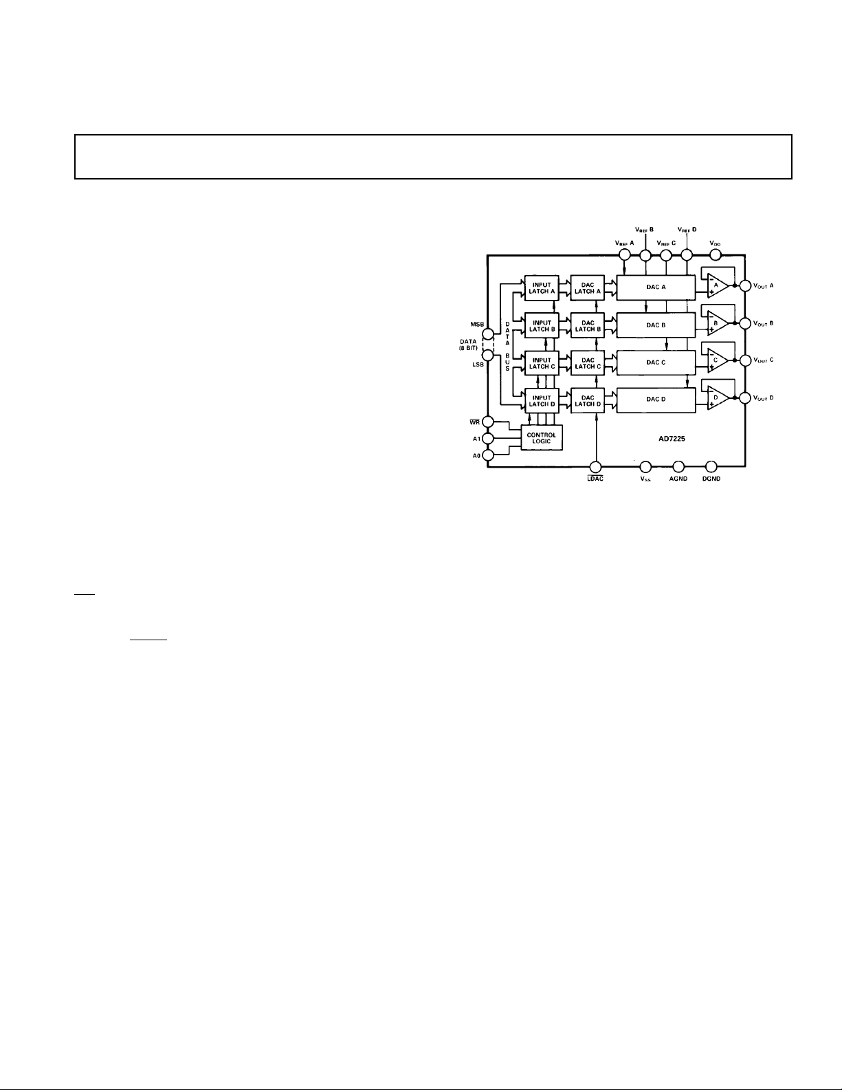
GENERAL DESCRIPTION
The AD7225 contains four 8-bit voltage output digital-toanalog converters, with output buffer amplifiers and interface
logic on a single monolithic chip. Each D/A converter has a
separate reference input terminal. No external trims are required to achieve full specified performance for the part.
The double-buffered interface logic consists of two 8-bit registers per channel–an input register and a DAC register. Control
inputs A0 and A1 determine which input register is loaded when
WR goes low. Only the data held in the DAC registers determines the analog outputs of the converters. The doublebuffering allows simultaneous update of all four outputs under
control of
level compatible and the control logic is speed compatible with
most 8-bit microprocessors.
Specified performance is guaranteed for input reference voltages
from +2 V to +12.5 V when using dual supplies. The part is also
specified for single supply operation using a reference of +10 V.
Each output buffer amplifier is capable of developing +10 V
across a 2 kΩ load.
The AD7225 is fabricated on an all ion-implanted high-speed
Linear Compatible CMOS (LC
specifically developed to integrate high speed digital logic circuits and precision analog circuitry on the same chip.
LDAC. All logic inputs are TTL and CMOS (5 V)
2
MOS) process which has been
with Separate Reference Inputs
AD7225
FUNCTIONAL BLOCK DIAGRAM
PRODUCT HIGHLIGHTS
1. DACs and Amplifiers on CMOS Chip
The single-chip design of four 8-bit DACs and amplifiers allows a dramatic reduction in board space requirements and
offers increased reliability in systems using multiple converters. Its pinout is aimed at optimizing board layout with all
analog inputs and outputs at one end of the package and all
digital inputs at the other.
2. Single or Dual Supply Operation
The voltage-mode configuration of the AD7225 allows single
supply operation. The part can also be operated with dual
supplies giving enhanced performance for some parameters.
3. Versatile Interface Logic
The AD7225 has a common 8-bit data bus with individual
DAC latches, providing a versatile control architecture for
simple interface to microprocessors. The double-buffered interface allows simultaneous update of the four outputs.
4. Separate Reference Input for Each DAC
The AD7225 offers great flexibility in dealing with input signals with a separate reference input provided for each DAC
and each reference having variable input voltage capability.
REV. B
Information furnished by Analog Devices is believed to be accurate and
reliable. However, no responsibility is assumed by Analog Devices for its
use, nor for any infringements of patents or other rights of third parties
which may result from its use. No license is granted by implication or
otherwise under any patent or patent rights of Analog Devices.
One Technology Way, P.O. Box 9106, Norwood, MA 02062-9106, U.S.A.
Tel: 617/329-4700 Fax: 617/326-8703

AD7225–SPECIFICA TIONS
DUAL SUPPLY
(VDD = 11.4 V to 16.5 V, VSS = –5 V 6 10%; AGND = DGND = O V; V
All specifications T
MIN
to T
unless otherwise noted.)
MAX
= +2 V to (VDD – 4 V)1 unless otherwise noted.
REF
K, B L, C
Parameter Versions2Versions2T Version U Version Units Conditions/Comments
STATIC PERFORMANCE
Resolution 8 8 8 8 Bits
Total Unadjusted Error ±2 ±1 ±2 ±1 LSB max V
Relative Accuracy ± 1 ± 1/2 ± 1 ±1/2 LSB max
= +15 V ± 5%, V
DD
REF
Differential Nonlinearity ± 1 ±1 ±1 ±1 LSB max Guaranteed Monotonic
Full-Scale Error ±1 ±1/2 ±1 ±1/2 LSB max
Full-Scale Temp. Coeff. ±5 ±5 ±5 ±5 ppm/°C typ VDD = 14 V to 16.5 V, V
Zero Code Error @ 25°C ±25 ±15 ±25 ±15 mV max
T
to T
MIN
Zero Code Error Temp Coeff. ±30 ±30 ±30 ±30 µV/°C typ
MAX
±30 ±20 ±30 ±20 mV max
REFERENCE INPUT
Voltage Range 2 to (VDD – 4) 2 to (VDD – 4) 2 to (VDD – 4) 2 to (VDD – 4) V min to V max
Input Resistance 11 11 11 11 kΩ min
Input Capacitance
Channel-to-Channel Isolation360 60 60 60 dB min V
AC Feedthrough
3
3
100 100 100 100 pF max Occurs when each DAC is loaded with all 1s.
= 10 V p-p Sine Wave @ 10 kHz
–70 –70 –70 –70 dB max V
REF
= 10 V p-p Sine Wave @ 10 kHz
REF
DIGITAL INPUTS
Input High Voltage, V
Input Low Voltage, V
Input Leakage Current ±1 ±1 ±1 ±1 µA max VIN = 0 V or V
Input Capacitance
INH
INL
3
2.4 2.4 2.4 2.4 V min
0.8 0.8 0.8 0.8 V max
8 8 8 8 pF max
DD
Input Coding Binary Binary Binary Binary
DYNAMIC PERFORMANCE
Voltage Output Slew Rate32.5 2.5 2.5 2.5 V/µs min
Voltage Output Settling Time
Positive Full-Scale Change 5 5 5 5 µs max V
Negative Full-Scale Change 5 5 5 5 µs max V
Digital Feedthrough
Digital Crosstalk
3
3
Minimum Load Resistance 2 2 2 2 kΩ min V
3
= +10 V; Settling Time to ±1/2 LSB
REF
= +10 V; Settling Time to ±1/2 LSB
50 50 50 50 nV secs typ Code transition all 0s to all 1s.
REF
50 50 50 50 nV secs typ Code transition all 0s to all 1s.
= +10 V
OUT
POWER SUPPLIES
VDD Range 11.4/16.5 11.4/16.5 11.4/16.5 11.4/16.5 V min to V max For Specified Performance
I
DD
I
SS
SWITCHING CHARACTERISTICS
t
1
@ 25°C 95 9 5 95 95 ns min Write Pulse Width
T
to T
MIN
MIN
MIN
MIN
MIN
MIN
to T
to T
to T
to T
to T
MAX
MAX
MAX
MAX
MAX
MAX
t
2
@ 25°C 0 0 0 0 ns min Address to Write Setup Time
T
t
3
@ 25°C 0 0 0 0 ns min Address to Write Hold Time
T
t
4
@ 25°C 70 7 0 70 70 ns min Data Valid to Write Setup Time
T
t
5
@ 25°C 10 1 0 10 10 ns min Data Valid to Write Hold Time
T
t
6
@ 25°C 95 9 5 95 95 ns min Load DAC Pulse Width
T
NOTES
1
Maximum possible reference voltage.
2
Temperature ranges are as follows:
K, L Versions: –40°C to +85°C
B, C Versions: –40°C to +85°C
T, U Versions: –55°C to +125°C
3
Sample Tested at 25°C to ensure compliance.
4
Switching characteristics apply for single and dual supply operation.
Specifications subject to change without notice.
10 10 12 12 mA max Outputs Unloaded; VIN = V
9 9 10 10 mA max Outputs Unloaded; VIN = V
3, 4
120 120 150 150 ns min
0 0 0 0 ns min
0 0 0 0 ns min
90 90 90 90 ns min
10 10 10 10 ns min
120 120 150 150 ns min
= +10 V
= +10 V
REF
or V
INL
or V
INL
INH
INH
–2–
REV. B

AD7225
(VDD = +15 V 6 5%; VSS = AGND = DGND = O V; V
SINGLE SUPPLY
Parameter Versions2Versions
All specifications T
K, B L, C
MIN
to T
MAX
unless otherwise noted.)
2
T Version U Version Units Conditions/Comments
= +10 V1 unless otherwise noted.
REF
STATIC PERFORMANCE
Resolution 8888Bits
Total Unadjusted Error
Differential Nonlinearity
3
3
±2 ±1 ±2 ±1 LSB max
± 1 ±1 ±1 ±1 LSB max Guaranteed Monotonic
REFERENCE INPUT
Input Resistance 11 11 11 11 kΩ min
Input Capacitance
Channel-to-Channel Isolation
AC Feedthrough
4
3, 4, 5
100 100 100 100 pF max Occurs when each DAC is loaded with all 1s.
3, 4
60 60 60 60 dB min V
–70 –70 –70 –70 dB max V
= 10 V p-p Sine Wave @ 10 kHz
REF
= 10 V p-p Sine Wave @ 10 kHz
REF
DIGITAL INPUTS
Input High Voltage, V
Input Low Voltage, V
Input Leakage Current ±1 ±1 ±1 ±1 µA max VIN = 0 V or V
Input Capacitance
INH
INL
4
2.4 2.4 2.4 2.4 V min
0.8 0.8 0.8 0.8 V max
8888pF max
DD
Input Coding Binary Binary Binary Binary
DYNAMIC PERFORMANCE
Voltage Output Slew Rate
Voltage Output Settling Time
4
2222V/µs min
4
Positive Full-Scale Change 5555µs max Settling Time to ±1/2 LSB
Negative Full-Scale Change 7777µs max Settling Time to ±1/2 LSB
Digital Feedthrough
Digital Crosstalk
Minimum Load Resistance 2222kΩ min V
3, 4
3, 4
50 50 50 50 nV secs typ Code transition all 0s to all 1s.
50 50 50 50 nV secs typ Code transition all 0s to all 1s.
= +10 V
OUT
POWER SUPPLIES
VDD Range 14.25/15.75 14.25/15.75 14.25/15.75 14.25/15.75 V min to V max For Specified Performance
I
DD
SWITCHING CHARACTERISTICS
t
1
@ 25°C 95 95 95 95 ns min Write Pulse Width
T
to T
MIN
MIN
MIN
MIN
MIN
MIN
to T
to T
to T
to T
to T
MAX
MAX
MAX
MAX
MAX
MAX
t
2
@ 25°C 0000ns minAddress to Write Setup Time
T
t
3
@ 25°C 0000ns minAddress to Write Hold Time
T
t
4
@ 25°C 70 70 70 70 ns min Data Valid to Write Setup Time
T
t
5
@ 25°C 10 10 10 10 ns min Data Valid to Write Hold Time
T
t
6
@ 25°C 95 95 95 95 ns min Load DAC Pulse Width
T
NOTES
1
Maximum possible reference voltage.
2
Temperature ranges are as follows:
K, L Versions: –40°C to +85°C
B, C Versions: –40°C to +85°C
T, U Versions: –55°C to +125°C
10 10 12 12 mA max Outputs Unloaded; VIN = V
4
120 120 150 150 ns min
0000ns min
0000ns min
90 90 90 90 ns min
10 10 10 10 ns min
120 120 150 150 ns min
3
Sample Tested at 25°C to ensure compliance.
4
Switching characteristics apply for single and dual supply operation.
Specifications subject to change without notice.
ORDERING GUIDE
INL
or V
INH
Total
Temperature Unadjusted Package
Range Error Option
Model
1
AD7225KN –40°C to +85°C ±2 LSB N-24
AD7225LN –40°C to +85° C ±1 LSB N-24
AD7225KP –40°C to +85°C ±2 LSB P-28A
AD7225LP –40°C to +85°C ±1 LSB P-28A
AD7225KR –40°C to +85° C ±2 LSB R-24
AD7225LR –40°C to +85° C ±1 LSB R-24
AD7225BQ –40°C to +85°C ±2 LSB Q-24
AD7225CQ –40°C to +85°C ±1 LSB Q-24
REV. B
Total
Temperature Unadjusted Package
Range Error Option
Model
1
2
AD7225TQ –55°C to +125°C ±2 LSB Q-24
AD7225UQ –55°C to +125°C ±1 LSB Q-24
AD7225TE –55°C to +125°C ±2 LSB E-28A
AD7225UE –55°C to +125 °C ±1 LSB E-28A
NOTES
1
To order MIL-STD-883 processed parts, add /883B to part number. Contact your
local sales office for military data sheet.
2
E = Leadless Ceramic Chip Carrier; N = Plastic DIP;
P = Plastic Leaded Chip Carrier; Q = Cerdip; R = SOIC.
–3–
2
AD7225
WARNING!
ESD SENSITIVE DEVICE
ABSOLUTE MAXIMUM RATINGS
1
VDD to AGND . . . . . . . . . . . . . . . . . . . . . . . . . .–0.3 V, +17 V
V
to DGND . . . . . . . . . . . . . . . . . . . . . . . . . .–0.3 V, +17 V
DD
V
to VSS . . . . . . . . . . . . . . . . . . . . . . . . . . . . .–0.3 V, +24 V
DD
AGND to DGND . . . . . . . . . . . . . . . . . . . . . . . . –0.3 V, V
DD
Digital Input Voltage to DGND . . . . . . . –0.3 V, VDD + 0.3 V
V
to AGND . . . . . . . . . . . . . . . . . . . . –0.3 V, VDD + 0.3 V
REF
V
to AGND2 . . . . . . . . . . . . . . . . . . . . . . . . . . . . VSS, V
OUT
DD
Power Dissipation (Any Package) to +75°C . . . . . . . . 500 mW
Derates above 75°C by . . . . . . . . . . . . . . . . . . . . . 2.0 mW/°C
Operating Temperature
Commercial (K, L Versions) . . . . . . . . . . . –40°C to +85°C
Industrial (B, C Versions) . . . . . . . . . . . . . –40°C to +85°C
Extended (T, U Versions) . . . . . . . . . . . . –55°C to +125°C
Storage Temperature . . . . . . . . . . . . . . . . . . –65°C to +150°C
Lead Temperature (Soldering, 10 secs) . . . . . . . . . . . +300°C
NOTES
1
Stresses above those listed under “Absolute Maximum Ratings” may cause
permanent damage to the device. This is a stress rating only and functional
operation of the device at these or any other conditions above those indicated in
the operational sections of this specification is not implied. Exposure to absolute
maximum rating conditions for extended periods may affect device reliability.
2
Outputs may be shorted to any voltage in the range VSS to VDD provided that the
power dissipation of the package is not exceeded. Typical short circuit current for
a short to AGND or VSS is 50 mA.
CAUTION
ESD (electrostatic discharge) sensitive device. Electrostatic charges as high as 4000 V readily
accumulate on the human body and test equipment and can discharge without detection.
Although the AD7225 features proprietary ESD protection circuitry, permanent damage may
occur on devices subjected to high energy electrostatic discharges. Therefore, proper ESD
precautions are recommended to avoid performance degradation or loss of functionality.
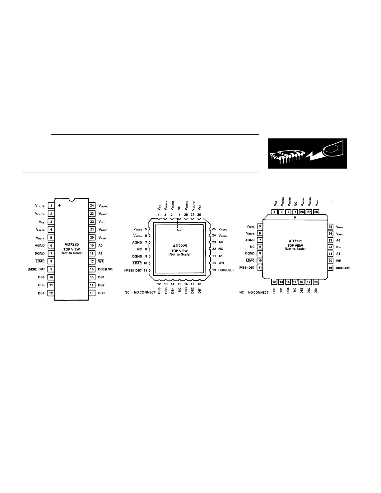
PIN CONFIGURATIONS
DIP and SOIC LCCC PLCC
TERMINOLOGY
TOTAL UNADJUSTED ERROR
Total Unadjusted Error is a comprehensive specification which
includes full-scale error, relative accuracy, and zero code error.
Maximum output voltage is V
(ideal) is V
/256. The LSB size will vary over the V
REF
– 1 LSB (ideal), where 1 LSB
REF
REF
Hence the zero code error will, relative to the LSB size, increase
as V
decreases. Accordingly, the total unadjusted error,
REF
which includes the zero code error, will also vary in terms of
LSBs over the V
range. As a result, total unadjusted error is
REF
specified for a fixed reference voltage of +10 V.
RELATIVE ACCURACY
Relative Accuracy or endpoint nonlinearity is a measure of the
maximum deviation from a straight line passing through the
endpoints of the DAC transfer function. It is measured after allowing for zero code error and full-scale error and is normally
expressed in LSBs or as a percentage of full-scale reading.
DIFFERENTIAL NONLINEARITY
Differential Nonlinearity is the difference between the measured
change and the ideal 1 LSB change between any two adjacent
codes. A specified differential nonlinearity of ± 1 LSB max over
the operating temperature range ensures monotonicity.
range.
DIGITAL FEEDTHROUGH
Digital Feedthrough is the glitch impulse transferred to the output of the DAC due to a change in its digital input code. It is
specified in nV secs and is measured at V
REF
= 0 V.
DIGITAL CROSSTALK
Digital Crosstalk is the glitch impulse transferred to the output
of one converter (not addressed) due to a change in the digital
input code to another addressed converter. It is specified in
nV secs and is measured at V
REF
= 0 V.
AC FEEDTHROUGH
AC Feedthrough is the proportion of reference input signal
which appears at the output of a converter when that DAC is
loaded with all 0s.
CHANNEL-TO-CHANNEL ISOLATION
Channel-to-channel isolation is the proportion of input signal
from the reference of one DAC (loaded with all 1s) which appears at the output of one of the other three DACs (loaded with
all 0s) The figure given is the worst case for the three other outputs and is expressed as a ratio in dBs.
FULL-SCALE ERROR
Full-Scale Error is defined as:
Measured Value – Zero Code Error – Ideal Value
–4–
REV. B

Typical Performance Characteristics–
TA = 258C, VDD = +15 V, VSS = –5 V unless otherwise noted.
AD7225
Figure 1. Channel-to-Channel Matching
Figure 3. Differential Nonlinearity vs. V
REF
Figure 2. Relative Accuracy vs. V
Figure 4. Power Supply Current vs. Temperature
REF
REV. B
Figure 5. Zero Code Error vs. Temperature
Figure 6. Broadband Noise
–5–

AD7225
CIRCUIT INFORMATION
D/A SECTION
The AD7225 contains four, identical, 8-bit voltage mode
digital-to-analog converters. Each D/A converter has a separate
reference input. The output voltages from the converters have
the same polarity as the reference voltages, allowing single supply operation. A novel DAC switch pair arrangement on the
AD7225 allows a reference voltage range from +2 V to +12.5 V
on each reference input.
Each DAC consists of a highly stable, thin-film, R-2R ladder
and eight high speed NMOS, single-pole, double-throw
switches. The simplified circuit diagram for channel A is shown
in Figure 7. Note that AGND (Pin 6) is common to all four
DACs.
Figure 7. D/A Simplified Circuit Diagram
The input impedance at any of the reference inputs is code dependent and can vary from 11 kΩ minimum to infinity. The
lowest input impedance at any reference input occurs when that
DAC is loaded with the digital code 01010101. Therefore, it is
important that the reference presents a low output impedance
under changing load conditions. The nodal capacitance at the
reference terminals is also code dependent and typically varies
from 15 pF to 35 pF.
Each V
pin can be considered as a digitally programmable
OUT
voltage source with an output voltage of:
V
= DX • V
OUTX
REFX
where DX is fractional representation of the digital input code
and can vary from 0 to 255/256.
The output impedance is that of the output buffer amplifier.
OP-AMP SECTION
Each voltage mode D/A converter output is buffered by a unity
gain noninverting CMOS amplifier. This buffer amplifier is capable of developing +10 V across a 2 kΩ load and can drive capacitive loads of 3300 pF.
The AD7225 can be operated single or dual supply; operating
with dual supplies results in enhanced performance in some parameters which cannot be achieved with single supply operation.
In single supply operation (V
= 0 V = AGND) the sink capa-
SS
bility of the amplifier, which is normally 400 µA, is reduced as
the output voltage nears AGND. The full sink capability of
400 µA is maintained over the full output voltage range by tying
V
to –5 V. This is indicated in Figure 8.
SS
Settling-time for negative-going output signals approaching
AGND is similarly affected by V
. Negative-going settling-time
SS
for single supply operation is longer than for dual supply operation. Positive-going settling-time is not affected by V
.
SS
Figure 8. Variation of I
SINK
with V
OUT
Additionally, the negative VSS gives more headroom to the output amplifiers which results in better zero code performance and
improved slew rate at the output, than can be obtained in the
single supply mode.
DIGITAL SECTION
The AD7225 digital inputs are compatible with either TTL or
5 V CMOS levels. All logic inputs are static protected MOS
gates with typical input currents of less than 1 nA. Internal input protection is achieved by an on-chip distributed diode between DGND and each MOS gate. To minimize power supply
currents, it is recommended that the digital input voltages be
driven as close to the supply rails (V
and DGND) as practi-
DD
cally possible.
INTERFACE LOGIC INFORMATION
The AD7225 contains two registers per DAC, an input register
and a DAC register. Address lines A0 and A1 select which input
register will accept data from the input port. When the
WR signal is LOW, the input latches of the selected DAC are transparent. The data is latched into the addressed input register on the
rising edge of
WR. Table I shows the addressing for the input
registers on the AD7225.
Table I. AD7225 Addressing
A1 A0 Selected Input Register
L L DAC A Input Register
L H DAC B Input Register
H L DAC C Input Register
H H DAC D Input Register
–6–
REV. B

Only the data held in the DAC register determines the analog
output of the converter. The
DACs and controls the transfer of information from the input
registers to the DAC registers. Data is latched into all four DAC
registers simultaneously on the rising edge of
LDAC signal is level triggered and therefore the DAC registers
may be made transparent by tying
outputs of the converters will respond to the data held in their
respective input latches).
is independent of
However, in systems where the asynchronous
during a write cycle (or vice versa) care must be taken to ensure
that incorrect data is not latched through to the output. In other
words, if
WR occurs during LDAC), then LDAC must stay LOW for t
or longer after WR goes HIGH to ensure correct data is latched
through to the output. Table II shows the truth table for AD7225
operation. Figure 9 shows the input control logic for the part
and the write cycle timing diagram is given in Figure 10.
WR LDAC Function
H H No Operation. Device not selected
L H Input Register of Selected DAC Transparent
g
H L All Four DAC Registers Transparent
H
L L DAC Registers and Selected Input Register
LDAC is activated prior to the rising edge of WR (or
H Input Register of Selected DAC Latched
g
WR. This is useful in many applications.
Table II. AD7225 Truth Table
(i.e. Outputs respond to data held in respective
input registers)
Input Registers are Latched
All Four DAC Registers Latched
Transparent Output follows Input Data for
Selected Channel.
LDAC signal is common to all four
LDAC. The
LDAC LOW (in this case the
LDAC is an asynchronous signal and
LDAC can occur
6
AD7225
Figure 9. Input Control Logic
Figure 10. Write Cycle Timing Diagram
GROUND MANAGEMENT AND LAYOUT
Since the AD7225 contains four reference inputs which can be
driven from ac sources (see AC REFERENCE SIGNAL section) careful layout and grounding is important to minimize
analog crosstalk between the four channels. The dynamic performance of the four DACs depends upon the optimum choice
of board layout. Figure 11 shows the relationship between input
Figure 11. Channel-to-Channel Isolation
Figure 12. Suggested PCB Layout for AD7225.
Layout Shows Component Side (Top View)
frequency and channel-to-channel isolation. Figure 12 shows a
printed circuit board layout which is aimed at minimizing
crosstalk and feedthrough. The four input signals are screened
by AGND. V
avoid slew rate limiting effects from the output amplifier during
measurements.
was limited to between 2 V and 3.24 V to
REF
REV. B
–7–

AD7225
+V
REF
255
256
SPECIFICATION RANGES
For the AD7225 to operate to rated specifications, its input reference voltage must be at least 4 V below the V
power supply
DD
voltage. This voltage differential is the overhead voltage required by the output amplifiers.
The AD7225 is specified to operate over a V
range from
DD
+12 V ± 5% to +15 V ±10% (i.e., from +11.4 V to +16.5 V)
with a V
+15 V ± 5% V
of –5 V ±10%. Operation is also specified for a single
SS
supply. Applying a VSS of –5 V results in im-
DD
proved zero code error, improved output sink capability with
outputs near AGND and improved negative going settling time.
Performance is specified over a wide range of reference voltages
from 2 V to (V
– 4 V) with dual supplies. This allows a range
DD
of standard reference generators to be used such as the AD580,
a +2.5 V bandgap reference and the AD584, a precision +10 V
reference. Note that an output voltage range of 0 V to +10 V requires a nominal +15 V ± 5% power supply voltage.
UNIPOLAR OUTPUT OPERATION
This is the basic mode of operation for each channel of the
AD7225, with the output voltage having the same positive
polarity as V
(V
= AGND) or with positive/negative supplies (see op-amp
SS
section which outlines the advantages of having negative V
. The AD7225 can be operated single supply
REF
).
SS
Connections for the unipolar output operation are shown in Figure 13. The voltage at any of the reference inputs must never be
negative with respect to DGND. Failure to observe this precaution may cause parasitic transistor action and possible device destruction. The code table for unipolar output operation is shown
in Table III.
Table III. Unipolar Code Table
DAC Latch Contents
MSB LSB Analog Output
1 1 1 1 1 1 1 1
1 0 0 0 0 0 0 1
1 0 0 0 0 0 0 0
0 1 1 1 1 1 1 1
0 0 0 0 0 0 0 1
+V
+V
+V
+V
REF
REF
REF
REF
129
256
128
256
127
256
1
256
V
REF
=+
2
0 0 0 0 0 0 0 0 0 V
Note: 1 LSB = V
−8
2
()
REF
=V
()
REF
1
256
BIPOLAR OUTPUT OPERATION
Each of the DACs of the AD7225 can be individually configured to provide bipolar output operation. This is possible using
one external amplifier and two resistors per channel. Figure 14
shows a circuit used to implement offset binary coding (bipolar
operation) with DAC A of the AD7225. In this case
OUT
= 1+
V
R2
⋅ D
()
AVREF
R1
R2
–
R1
⋅V
()
REF
With R1 = R2
= (2 DA – 1) • V
V
OUT
REF
where DA is a fractional representation of the digital word in
latch A. (0 ≤ D
≤ 255/256)
A
Mismatch between R1 and R2 causes gain and offset errors and,
therefore, these resistors must match and track over temperature. Once again the AD7225 can be operated in single supply
or from positive/negative supplies. Table IV shows the digital
code versus output voltage relationship for the circuit of Figure
14 with R1 = R2.
Figure 13. Unipolar Output Circuit
–8–
REV. B

Figure 14. AD7225 Bipolar Output Circuit
Table IV. Bipolar (Offset Binary) Code Table
DAC Latch Contents
MSB LSB Analog Output
1 1 1 1 1 1 1 1
1 0 0 0 0 0 0 1
+V
+V
REF
REF
127
128
1
128
1 0 0 0 0 0 0 0 0 V
AD7225
For a given VIN, increasing AGND above system GND will reduce the effective V
DD–VREF
sure specified operation. Note that because the AGND pin is
common to all four DACs, this method biases up the output
voltages of all the DACs in the AD7225. Note that V
of the AD7225 should be referenced to DGND.
AC REFERENCE SIGNAL
In some applications it may be desirable to have ac reference
signals. The AD7225 has multiplying capability within the upper (V
– 4 V) and lower (2 V) limits of reference voltage when
DD
operated with dual supplies. Therefore ac signals need to be ac
coupled and biased up before being applied to the reference inputs. Figure 16 shows a sine wave signal applied to V
input signal frequencies up to 50 kHz the output distortion typically remains less than 0.1%. The typical 3 dB bandwidth figure
for small signal inputs is 800 kHz.
which must be at least 4 V to en-
and V
DD
A. For
REF
SS
0 1 1 1 1 1 1 1
0 0 0 0 0 0 0 1
0 0 0 0 0 0 0 0
–V
–V
–V
REF
REF
REF
1
128
127
128
128
128
= –V
REF
AGND BIAS
The AD7225 AGND pin can be biased above system GND
(AD7225 DGND) to provide an offset “zero” analog output
voltage level. Figure 15 shows a circuit configuration to achieve
this for channel A of the AD7225. The output voltage, V
OUT
A,
can be expressed as:
V
A = V
OUT
where D
DAC latch A. (0 ≤ D
+ DA (VIN)
BIAS
is a fractional representation of the digital word in
A
≤ 255/256).
A
Figure 16. Applying an AC Signal to the AD7225
APPLICATIONS
PROGRAMMABLE TRANSVERSAL FILTER
A discrete-time filter may be described by either multiplication
in the frequency domain or convolution in the time domain i.e.
Y ω
()
=Hω
()
Xω
()
or yn=∑
N
k=1
h
kXn–k+1
The convolution sum may be implemented using the special
structure known as the transversal filter (Figure 17). Basically, it
consists of an N-stage delay line with N taps weighted by N coefficients, the resulting products being accumulated to form the
output. The tap weights or coefficients h
are actually the non-
k
zero elements of the impulse response and therefore determine
the filter transfer function. A particular filter frequency response
is realized by setting the coefficients to the appropriate values.
This property leads to the implementation of transversal filters
whose frequency response is programmable.
REV. B
Figure 15. AGND Bias Circuit
Figure 17. Transversal Filter
–9–

AD7225
DELAYED
FILTER
I/P
AD7820
ADC
SAMPLES
AD584
+10V V
REF
I/P
Am29520
TLD
Am7224
DAC
V
REF
GAIN SET
I/P
SAMPLES
OUT
V
REF
h
1
V
A
REF
h
V
A
OUT
TAP WEIGHTS
QUAD DAC
V
2
V
QUAD DAC
AD7225
A
REF
A
OUT
AD7226
V
REF
h
3
V
OUT
Figure 18. Programmable Transversal Filter
A 4-tap programmable transversal filter may be implemented
using the AD7225 (Figure 18). The input signal is first sampled
and converted to allow the tapped delay line function to be provided by the Am29520. The multiplication of delayed input
samples by fixed, programmable up weights is accomplished by
the AD7225, the four coefficients or reference inputs being set
by the digital codes stored in the AD7226. The resultant products are accumulated to yield the convolution sum output
sample which is held by the AD585.
0
–10
–20
–30
–40
–50
–60
GAIN – dB
–70
–80
–90
–100
0
h1 = 0.117
h2 = 0.417
h3 = 0.417
h4 = 0.417
0.05
NORMALIZED FREQUENCY – f/fs
0.5
0.450.40.350.30.250.20.150.1
Figure 19. Predicted (Theoretical) Response
FILTER
I/P
ACCUMULATOR
O/P
+
X
n
T T T
1234
1
h
2
h
AD585
SHA
X
n–1
FILTER
O/P
X
n–2
h
3
h
4
X
n–3
V
A
OUT
V
B
OUT
V
C
OUT
V
D
OUT
A
A
V
REF
h
4
V
A
A
OUT
+
FILTER
O/P
Y
n
filter with the coefficients indicated. Although the theoretical
prediction does not take into account the quantization of the input samples and the truncation of the coefficients, nevertheless,
there exists a good correlation with the actual performance of
the transversal filter (Figure 20).
DIGITAL WORD MULTIPLICATION
Since each DAC of the AD7225 has a separate reference input,
the output of one DAC can be used as the reference input for
another. This means that multiplication of digital words can be
performed (with the result given in analog form). For example,
if the output from DACA is applied to V
from DACB, V
B = DA • DB • V
V
OUT
where D
A
B, can be expressed as:
OUT
A
REF
and DB are the fractional representations of the
B then the output
REF
digital words in DAC latches A and B respectively.
If D
= DB = D then the result is D2 • V
A
REF
A
In this manner, the four DACs can be used on their own or in
conjunction with an external summing amplifier to generate
complex waveforms. Figure 21 shows one such application. In
this case the output waveform, Y, is represented by:
4
Y = –(x
+ 2x3 + 3x2 + 2x + 4) • V
IN
where x is the digital code which is applied to all four DAC
latches.
Figure 20. Actual Response
Low pass, bandpass and high pass filters may be synthesized using this arrangement. The particular up weights needed for any
desired transfer function may be obtained using the standard
Remez Exchange Algorithm. Figure 19 shows the theoretical
low pass frequency response produced by a 4-tap transversal
–10–
+15V
V
DD
V
V
V
IN
REF
V
REF
V
REF
V
REF
A
AD7225*
B
C
D
DGNDAGND
A
OUT
V
B
OUT
V
C
OUT
V
D
OUT
V
SS
25kΩ
50kΩ
33kΩ
50kΩ
100kΩ
*DIGITAL INPUTS OMITTED
FOR CLARITY
Figure 21. Complex Waveform Generation
100kΩ
Y
REV. B

MICROPROCESSOR INTERFACE
68008
A23
A1
D0
D7
AD7225*
R/W
A0
A1
DB7
DB0
LDAC
WR
ADDRESS BUS
DATA BUS
*LINEAR CIRCUITRY OMITTED FOR CLARITY
ADDRESS
DECODE
EN
AS
DTACK
AD7225
8085A/
8088
ALE
AD7
AD0
A15
WR
A8
LATCH
EN
*
LINEAR CIRCUITRY OMITTED FOR CLARITY
ADDRESS BUS
ADDRESS
DECODE
ADDRESS DATA BUS
A0
A1
LDAC
AD7225*
WR
DB7
DB0
Figure 22. AD7225 to 8085A/8088 Interface,
Double-Buffered Mode
A15
A0
6809/
6502
R/W
E OR φ2
D7
D0
ADDRESS
DECODE
EN
*
ADDRESS BUS
A0
A1
LDAC
AD7225*
WR
DB7
DB0
DATA BUS
LINEAR CIRCUITRY OMITTED FOR CLARITY
Figure 23. AD7225 to 6809/6502 Interface,
Single-Buffered Mode
Z-80
MREQ
A15
WR
A8
D7
D0
*
ADDRESS BUS
A0
ADDRESS
DECODE
EN
DATA BUS
LINEAR CIRCUITRY OMITTED FOR CLARITY
A1
LDAC
AD7225*
WR
DB7
DB0
Figure 24. AD7225 to Z-80 Interface,
Double-Buffered Mode
Figure 25. AD7225 to 68008 Interface,
Single-Buffered Mode
VSS GENERATION
Operating the AD7225 from dual supplies results in enhanced
performance over single supply operation on a number of parameters as previously outlined. Some applications may require
this enhanced performance, but may only have a single power
supply rail available. The circuit of Figure 26 shows a method of
generating a negative voltage using one CD4049, operated from
a V
of +15 V. Two inverters of the hex inverter chip are used
DD
as an oscillator. The other four inverters are in parallel and used
as buffers for higher output current. The square-wave output is
level translated to a negative-going signal, then rectified and filtered. The circuit configuration shown will provide an output
voltage of –5.1 V for current loadings in the range 0.5 mA to
9 mA. This will satisfy the AD7225 I
requirement over the
SS
commercial operating temperature range.
1/6
CD4049AE
1/6
CD4049AE
510k
1/6
CD4049AE
5.1k
0.02µF
1/6
CD4049AE
1/6
CD4049AE
1/6
CD4049AE
47µF
1N4001
+
1N4001
+
510Ω
47µF
5V1
–V
OUT
Figure 26. VSS Generation Circuit
REV. B
–11–

AD7225
OUTLINE DIMENSIONS
Dimensions shown in inches and (mm).
24-Pin Plastic (N-24)
24-Pin Cerdip (Q-24)
24-Lead SOIC (R-24)
C927a–5–5/86
28-Terminal Leadless
Ceramic Chip Carrier (E-28A)
28-Lead PLCC (P-28A)
–12–
PRINTED IN U.S.A.
REV. B
 Loading...