Differential, Low Noise IF Gain
a
FEATURES
24 dB Gain
4 dB Noise Figure
Easy Match to SAW Filters
Output Limiter Adjustable +8.5 dBm to +12 dBm
700 MHz Bandwidth
10 V Single or Dual 5 V Power Supply
300 mW Power Dissipation
APPLICATIONS
ADC IF Drive Amp
Communications Receivers
PCS/Cellular Base Stations
GSM, CDMA, TDMA
PRODUCT DESCRIPTION
The AD6630 is an IF gain block designed to interface between
SAW filters and differential input analog-to-digital converters.
The AD6630 has a fixed gain of 24 dB and has been optimized
for use with the AD6600 and AD6620 in digitizing narrowband
IF carriers in the 70 MHz to 250 MHz range.
Taking advantage of the differential nature of SAW filters, the
AD6630 has been designed as a differential in/differential out
gain block. This architecture allows 100 dB of adjacent channel
blocking using low cost SAW filters. The AD6630 provides
output limiting for ADC and SAW protection with ⬍10° phase
variation in recovery from overdrive situations.
Designed for “narrow-band” cellular/PCS receivers, the high
linearity and low noise performance of the AD6630 allows for
implementation in a wide range of applications ranging from
Block with Output Clamping
AD6630
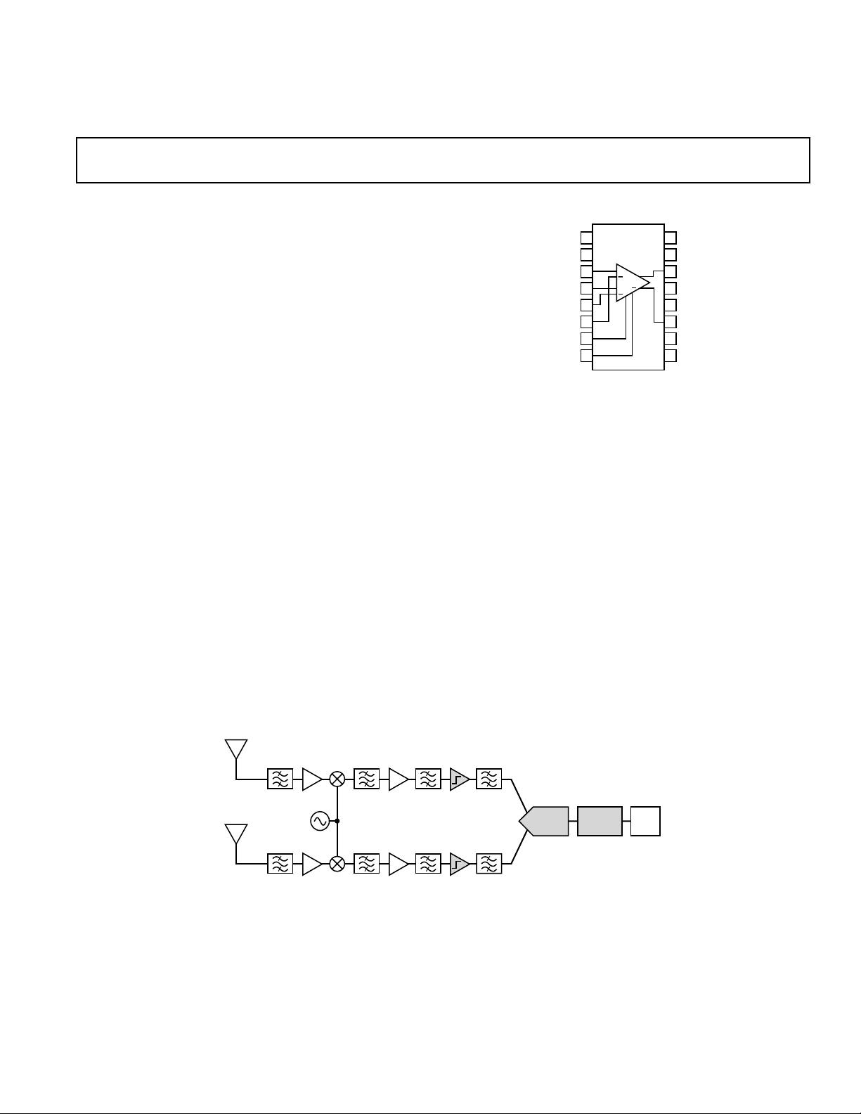
FUNCTIONAL BLOCK DIAGRAM
AD6630
1
NC
2
NC
+
3
IP2
4
IP1
IP1
IP2
CLLO
CLHI
+
5
6
7
8
NC = NO CONNECT
GSM to CDMA to AMPS. The clamping circuitry also maintains the phase integrity of an overdriven signal. This allows
phase demodulation of single carrier signals with an overrange
signal.
While the AD6630 is optimized for use with the AD6600 Dual
Channel, Gain Ranging ADC with RSSI, it can also be used in
many other IF applications. The AD6630 is designed with an
input impedance of 200 Ω and an output of 400 Ω. In the typi-
cal application shown below, these values match the real portion
of a typical SAW filter. Other devices can be matched using
standard matching network techniques.
The AD6630 is built using Analog Devices’ high speed complementary bipolar process. Units are available in a 300 mil SOIC
(16 leads) plastic surface mount package and specified to operate
over the industrial temperature range (–40°C to +85°C).
16
V
CC
15
CD1
14
+
OP
13
V
EE
12
CMD
11
OP
10
CD2
9
V
CC
LOCAL
OSCILLATOR
Figure 1. Reference Design
REV. 0
Information furnished by Analog Devices is believed to be accurate and
reliable. However, no responsibility is assumed by Analog Devices for its
use, nor for any infringements of patents or other rights of third parties
which may result from its use. No license is granted by implication or
otherwise under any patent or patent rights of Analog Devices.
AD6630
MAIN
AD6600
AD6630
One Technology Way, P.O. Box 9106, Norwood, MA 02062-9106, U.S.A.
Tel: 781/329-4700 World Wide Web Site: http://www.analog.com
Fax: 781/326-8703 © Analog Devices, Inc., 1998
DIVERSITY
AD6620 DSP
AD6620

AD6630–SPECIFICATIONS
NORMAL OPERATING CONDITIONS
Parameter (Conditions) Min Typ Max Units
SINGLE SUPPLY VOLTAGE 8.5 10.5 V
POSITIVE SUPPLY VOLTAGE 4.25 5.0 5.25 V
NEGATIVE SUPPLY VOLTAGE –5.25 –5.0 –4.25 V
AMBIENT TEMPERATURE –40 +85 °C
PACKAGE THERMAL RESISTANCE 80 °C/W
OPERATING FREQUENCY
DC SPECIFICATIONS
Parameter Temp Level Min Typ Max Units
SUPPLY CURRENT Full II 30 48 mA
OUTPUT DC LEVEL Full II VM–150 VM+150 mV
AC SPECIFICATIONS
1
(T
MIN
= –40ⴗC, T
= +85ⴗC. Output dc levels are nominally at VM, where VM = VCC + VEE = [+5 V + (–5 V)] = 0.
MAX
70 250 MHz
Inputs should be AC coupled.)
Test
(T
= –40ⴗC, T
MIN
= +85ⴗC. All AC production tests are performed at 5 MHz. 70 MHz and 250 MHz
MAX
performance limits are correlated to 5 MHz testing based on characterization data.)
Test
Parameter
1
Temp Level Min Typ Max Units
GAIN (POWER) @ 70 MHz Full II 23 24 25 dB
GAIN (POWER) @ 250 MHz Full II 22 23 24 dB
–3 dB BANDWIDTH +25°C V 700 MHz
OUTPUT REFERRED IP3 @ 70 MHz
OUTPUT REFERRED IP3 @ 250 MHz
OUTPUT REFERRED IP2 @ 70 MHz
OUTPUT REFERRED IP2 @ 250 MHz
OUTPUT REFERRED 1 dB COMPRESSION POINT
@ 70 MHz LOW LEVEL CLAMP
OUTPUT REFERRED 1 dB COMPRESSION POINT
@ 250 MHz LOW LEVEL CLAMP
OUTPUT REFERRED 1 dB COMPRESSION POINT
@ 70 MHz HIGH LEVEL CLAMP
OUTPUT REFERRED 1 dB COMPRESSION POINT
@ 250 MHz HIGH LEVEL CLAMP
2
2
2
2
3
3
4
4
Full V 22 dBm
Full V 19 dBm
Full V 45 dBm
Full V 45 dBm
Full II 8.5 dBm
Full II 7.5 dBm
Full II 11 dBm
Full II 9 dBm
OUTPUT SLEW RATE +25°C V 3700 V/µs
INPUT IMPEDANCE (REAL) +25°C V 200 Ω
INPUT CAPACITANCE +25°CV 2 pF
OUTPUT IMPEDANCE (REAL) +25°C V 400 Ω
OUTPUT CAPACITANCE +25°CV 2 pF
NOISE FIGURE +25°CV 4 dB
LOW LEVEL CLAMP MAXIMUM OUTPUT @ 70 MHz
HIGH LEVEL CLAMP MAXIMUM OUTPUT @ 70 MHz
LOW LEVEL CLAMP MAXIMUM OUTPUT @ 250 MHz
3, 5
4, 5
3, 5
Full IV 11 12.5 dBm
Full IV 13.8 14.3 dBm
Full IV 9.25 10.6 dBm
–2– REV. 0

AD6630
WARNING!
ESD SENSITIVE DEVICE
Test
Parameter Temp Level Min Typ Max Units
HIGH LEVEL CLAMP MAXIMUM OUTPUT @ 250 MHz
PHASE VARIATION
7
CMRR
8
PSRR
NOTES
1
All specifications are valid across the operating frequency range when the source and load impedance are a conjugate match to the amplifier’s input and output
impedance.
2
Test is for two tones separated by 1 MHz for IFs at 70 MHz and 250 MHz at –23 dBm per tone input.
3
Low Level Clamp is selected by connecting pin CLLO to the negative supply, while pin CLHI is left floating. Clamping can be set at lower levels by connecting pin
CLLO and CLHI to the negative supply through an external resistor.
4
High Level Clamp is selected by connecting pin CLHI to the negative supply, while pin CLLO is left floating, this allows the maximum linear range of the device to
be utilized.
5
Output clamp levels are measured for hard clamping with a +3 dBm input level. Valid for a maximum input level of +8 dBm/200 Ω = 3.2 V p-p—differential.
6
Measured as the change in output phase when the input level is changed from –53 dBm to +8 dBm (i.e., from linear operation to clamping).
7
Ratio of the differential output signal (referenced to the input) to the common-mode input signal presented to all input pins.
8
Ratio of signal on supply to differential output (<500 kHz).
Specifications subject to change without notice.
6
4, 5
Full IV 11.2 12.2 dBm
+25°C V 9 Degree
+25°CV 50 dB
+25°CV 30 dB
ABSOLUTE MAXIMUM RATINGS
EXPLANATION OF TEST LEVELS
I. 100% production tested.
Parameter Min Max Units
Single Supply Voltage –0.5 11.5 V
Positive Supply Voltage –0.5 5.75 V
Negative Supply Voltage –5.75 0.5 V
Input Power +8 dBm
Storage Temperature –65 +150 °C
Junction Temperature +150 °C
ESD Protection 1 kV
II. 100% production tested at +25°C, and guaranteed by
design and analysis at temperature extremes.
III. Sample tested only.
IV. Parameter guaranteed by design and analysis.
V. Parameter is typical value only.
VI. 100% production tested at +25°C, and sample tested at
temperature extremes.
ORDERING GUIDE
Model Temperature Range Package Description Package Option
AD6630AR –40°C to +85°C (Ambient) 16-Lead Wide Body SOIC R-16
AD6630AR-REEL –40°C to +85°C (Ambient) AD6630AR on 1000 PC Reel
AD6630R/PCB Evaluation Board with AD6630AR
CAUTION
ESD (electrostatic discharge) sensitive device. Electrostatic charges as high as 4000 V readily
accumulate on the human body and test equipment and can discharge without detection.
Although the AD6630 features proprietary ESD protection circuitry, permanent damage may
occur on devices subjected to high energy electrostatic discharges. Therefore, proper ESD
precautions are recommended to avoid performance degradation or loss of functionality.
–3–REV. 0
 Loading...