Analog Devices AD6622 Datasheet

Four-Channel, 75 MSPS Digital
a
FEATURES
Wideband Digital IF Parallel Output
Wideband Digital IF Parallel Input
Allows Cascade of Chips for Additional Channels
Programmable IF and Modulation for Each Channel
Programmable Interpolating RAM Coefficient Filter
High-Speed CIC Interpolating Filter
NCO Frequency Translation
Worst Spur Better than 100 dBc
Tuning Resolution Better than 0.02 Hz
Real or Complex Outputs
Digital Summation of Channels
Clipped or Wrapped Overrange
Two’s Complement or Offset Binary Output
Separate 3-Wire Serial Data Input for Each Channel
Microprocessor Control
JTAG Boundary Scan
APPLICATIONS
Cellular/PCS Base Stations
Micro/Pico Cell Base Stations
WBCDMA
Wireless Local Loop Base Stations
Phase Array Beam Forming Antennas
Transmit Signal Processor (TSP)
AD6622
FUNCTIONAL BLOCK DIAGRAM
CH A
CH B
CH C
CH D
SPORT
SPORT
SPORT
SPORT
JTAG
RCF
RCF
RCF
RCF
CIC
FILTER
CIC
FILTER
CIC
FILTER
CIC
FILTER
PORT
NCO
NCO
NCO
NCO
18
SUMMATION
18
PRODUCT DESCRIPTION
The AD6622 comprises four identical digital Transmit Signal
Processors (TSPs) complete with synchronization circuitry and
cascadable wideband channel summation. An external digitalto-analog converter (DAC) is all that is required to complete a
wide band digital up-converter. On-chip tuners allow the relative
phase and frequency for each RF carrier to be independently
controlled.
Each TSP has three cascaded signal processing elements: a
RAM-programmable Coefficient interpolating Filter (RCF), a
programmable Cascaded Integrator Comb (CIC) interpolating
filter, and a Numerically Controlled Oscillator/tuner (NCO).
The outputs of the four TSPs are summed and scaled on-chip.
REV. 0
Information furnished by Analog Devices is believed to be accurate and
reliable. However, no responsibility is assumed by Analog Devices for its
use, nor for any infringements of patents or other rights of third parties
which may result from its use. No license is granted by implication or
otherwise under any patent or patent rights of Analog Devices.
In multichannel wideband transmitters, multiple AD6622s may
be combined using the chip’s cascadable output summation stage.
Each channel provides independent serial data inputs that may
be directly connected to the serial port of DSP chips. User programmable FIR filters can be used to filter linear inputs.
All control registers and coefficient values are programmed through
a generic microprocessor interface. Two microprocessor bus
modes are supported. All inputs and outputs are LVCMOS
compatible. All outputs are LVCMOS and 5 V TTL compatible.
One Technology Way, P.O. Box 9106, Norwood, MA 02062-9106, U.S.A.
Tel: 781/329-4700 World Wide Web Site: http://www.analog.com
Fax: 781/326-8703 © Analog Devices, Inc., 2000

AD6622–SPECIFICATIONS
RECOMMENDED OPERATING CONDITIONS
Test AD6622AS
Parameter Level Min Typ Max Unit
VDD IV 2.4 3.0 3.3 V
T
AMBIENT
ELECTRICAL CHARACTERISTICS
Parameter (Conditions) Temp Level Min Typ Max Unit
LOGIC INPUTS (5 V TOLERANT) 3.0 V CMOS
Logic Compatibility Full
Logic “1” Voltage Full IV 2.0 VDD + 0.3 V
Logic “0” Voltage Full IV –0.3 +0.8 V
Logic “1” Current Full IV 1 10 µA
Logic “0” Current Full IV 1 10 µA
Input Capacitance 25°CV 4 pF
LOGIC OUTPUTS
Logic Compatibility Full
Logic “1” Voltage (I
Logic “0” Voltage (IOL = 0.25 mA) Full IV 0.02 0.05 V
IDD SUPPLY CURRENT
CLK = 60 MHz, 3.3 V
CLK = GSM Example V 297
CLK = IS-136 Example V 240
CLK = WBCDMA Example V 209
Sleep Mode Full IV 0.1 0.5 mA
POWER DISSIPATION
CLK = 60 MHz, 3.3 V
CLK = GSM Example V 0.89
CLK = IS-136 Example V 0.72
CLK = WBCDMA Example V 0.627
Sleep Mode Full IV 0.33 1.65 mW
NOTES
1
This specification denotes an absolute maximum supply current for the device. The conditions include all channels active, minimum interpolation in both CIC stages,
maximum switching of input data, and maximum VDD of 3.3 V. In an actual application the power will be less; see the Thermal Management section of the data sheet
for further details.
2
GSM interpolation = 120 at 65 MHz, 4 channels active, IS-136 interpolation = 2560 at 62.208 MHz, 4 channels active. WBCDMA interpolation = 64, 4 channels
interleaved at 61.44 MHz.
Specifications subject to change without notice.
= 0.25 mA) Full IV VDD – 0.05 VDD – 0.035 V
OH
1
1
Full IV 506 566
Full IV 1.77 1.87 W
IV –40 +25 +70 °C
Test AD6622AS
1
2
2
2
2
2
2
mA
mA
mA
mA
W
W
W
–2–
REV. 0

AD6622
TIMING CHARACTERISTICS
1
(C
= 40 pF, all outputs unless specified)
LOAD
Test AD6622AS
Name Parameter (Conditions) Temp Level Min Typ Max Unit
CLK Timing Requirements:
t
CLK
t
CLKL
t
CLKH
CLK Period Full IV 13.3 ns
CLK Width Low Full IV 5.5 0.5 × t
CLK Width High Full IV 5.5 0.5 × t
CLK
CLK
ns
ns
RESET Timing Requirements:
t
RESL
RESET Width Low Full IV 30.0 ns
Input Wideband Data Timing Requirements:
t
SI
t
HI
Input to CLK Setup Time Full IV 0.5 ns
Input to CLK Hold Time Full IV 3.5 ns
Parallel Output Switching Characteristics:
t
SO
t
HO
t
ZO
CLK to Output Setup Time Full IV 12 ns
CLK to Output Hold Time Full IV 4.1 ns
Output Three-State Time Full V 5 ns
SYNC Timing Requirements:
t
SS
t
HS
SYNC to CLK Setup Time Full IV 2.6 ns
SYNC to CLK Hold Time Full IV 1.5 ns
Serial Port Timing Requirements:
t
DSCLK
t
DSDFS
t
SSI
t
HSI
t
SCS
CLK to SCLK Delay Full V 8.5 ns
SCLK to SDFS Delay Full IV –1.2 +2.4 ns
SDI to SCLK Setup Time Full IV 8.5 ns
SDI to SCLK Hold Time Full IV 5.5 ns
Serial Clock Skew Full IV 7 ns
MICROPROCESSOR PORT, MODE INM (MODE = 0)
MODE INM Write Timing:
t
HWR
t
SAM
t
HAM
t
DRDY
t
FAST WR(R/W) to RDY(DTACK) High Delay Full IV 2 × t
ACC
MEDIUM WR(R/W) to RDY(DTACK) High Delay Full IV 3 × t
t
ACC
t
SLOW WR(R/W) to RDY(DTACK) High Delay Full IV 4 × t
ACC
WR(R/W) to RDY(DTACK) Hold Time Full IV 0 ns
Address/Data to WR(R/W) Setup Time Full IV 0 ns
Address/Data to RDY(DTACK) Hold Time Full IV 0 ns
WR(R/W) to RDY(DTACK) Delay Full IV 10.2 ns
CLK
CLK
CLK
3 × t
4 × t
5 × t
CLK
CLK
CLK
ns
ns
ns
MODE INM Read Timing:
t
SAM
t
HA
t
ZD
t
DD
t
DRDY
FAST RD(DS) to RDY(DTACK) High Delay Full IV 2 × t
t
ACC
t
MEDIUM RD(DS) to RDY(DTACK) High Delay Full IV 3 × t
ACC
t
SLOW RD(DS) to RDY(DTACK) High Delay Full IV 4 × t
ACC
Address to RD(DS) Setup Time Full IV 0 ns
Address to Data Hold Time Full IV 0 ns
Data Three-State Delay Full IV 3.4 7 10.5 ns
RDY(DTACK) to Data Delay Full IV t
– 10 ns
CLK
RD(DS) to RDY(DTACK) Delay Full IV 10.2 ns
CLK
CLK
CLK
3 × t
4 × t
5 × t
CLK
CLK
CLK
ns
ns
ns
REV. 0
–3–
AD6622
Test AD6622AS
Name Parameter (Conditions) Temp Level Min Typ Max Unit
MICROPROCESSOR PORT, MODE MNM (MODE = 1)
MODE MNM Write Timing:
t
HDS
t
HRW
t
SAM
t
HAM
t
DDTACK
FAST R/W(WR) to DTACK(RDY) Low Delay Full IV 2 × t
t
ACC
t
MEDIUM R/W(WR) to DTACK(RDY) Low Delay Full IV 3 × t
ACC
t
SLOW R/W(WR) to DTACK(RDY) Low Delay Full IV 4 × t
ACC
MODE MNM Read Timing:
t
SAM
t
HA
t
ZD
t
DD
t
DDTACK
t
FAST DS(RD) to DTACK(RDY) Low Delay Full IV 2 × t
ACC
t
MEDIUM DS(RD) to DTACK(RDY) Low Delay Full IV 3 × t
ACC
t
SLOW DS(RD) to DTACK(RDY) Low Delay Full IV 4 × t
ACC
NOTES
1
All Timing Specifications valid over VDD range of 2.4 V to 3.3 V.
Specifications subject to change without notice.
DS(RD) to DTACK(RDY) Hold Time Full IV 0 ns
R/W(WR) to DTACK(RDY) Hold Time Full IV 0 ns
Address/Data to R/W(WR) Setup Time Full IV 0 ns
Address/Data to R/W(WR) Hold Time Full IV 0 ns
DS(RD) to DTACK(RDY) Delay Full IV 1 × t
CLK
CLK
CLK
3 × t
4 × t
5 × t
CLK
CLK
CLK
CLK
ns
ns
ns
ns
Address to DS(RD) Setup Time Full IV 0 ns
Address to Data Hold Time Full IV 0 ns
Data Three-State Delay Full IV 0 ns
DTACK(RDY) to Data Delay Full IV t
DS(RD) to DTACK(RDY) Delay Full IV 1 × t
CLK
CLK
CLK
– 10 ns
CLK
CLK
3 × t
CLK
4 × t
CLK
5 × t
CLK
ns
ns
ns
ns
t
CLK
t
CLKL
CLK
OUT[17:0],
QOUT
OEN
t
CLKH
t
SO
t
t
ZO
HO
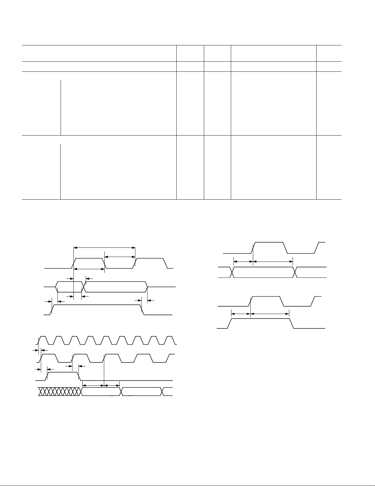
Figure 1. Parallel Output Switching Characteristics
CLK
t
DSCLK
SCLK
SDFS
SDI
t
DSDFS
t
DSDFS
t
SSI
DATAn
CLKn
t
HSI
Figure 2. Serial Port Switching Characteristics
CLK
t
HI
IN[17:0],
QIN
t
SI
Figure 3. Wideband Input Timing
t
ZO
CLK
SYNC
t
SS
t
HS
Figure 4. SYNC Timing Inputs
–4–
REV. 0
RD (DS)
CC
WR (R/W)
CS
t
AD6622
HWR
t
SAM
A[2:0]
D[7:0]
RDY
(DTACK)
ACCESS TIME DEPENDS ON THE ADDRESS ACCESSED. ACCESS TIME IS MEASURED FROM THE FE OF WR TO THE RE OF RDY.
1. t
ACC
FAST REQUIRES A MAXIMUM OF THREE CLK PERIODS AND APPLIES TO A[2:0] = 7, 6, 5, 3, 2, 1
2. t
ACC
MEDIUM REQUIRES A MAXIMUM OF FOUR CLK PERIODS AND APPLIES TO A[2:0] = 4 AND 0 IF THE ACCESS IS TO A CONTROL REGISTER
3. t
ACC
VERSUS A RAM REGISTER.
SLOW REQUIRES A MAXIMUM OF FIVE CLK PERIODS AND APPLIES TO A[2:0] = 0 WHEN ACCESSING RAM REGISTERS.
4. t
ACC
VALID ADDRESS
t
SAM
VALID DATA
t
DRDY
t
ACC
t
t
HAM
HAM
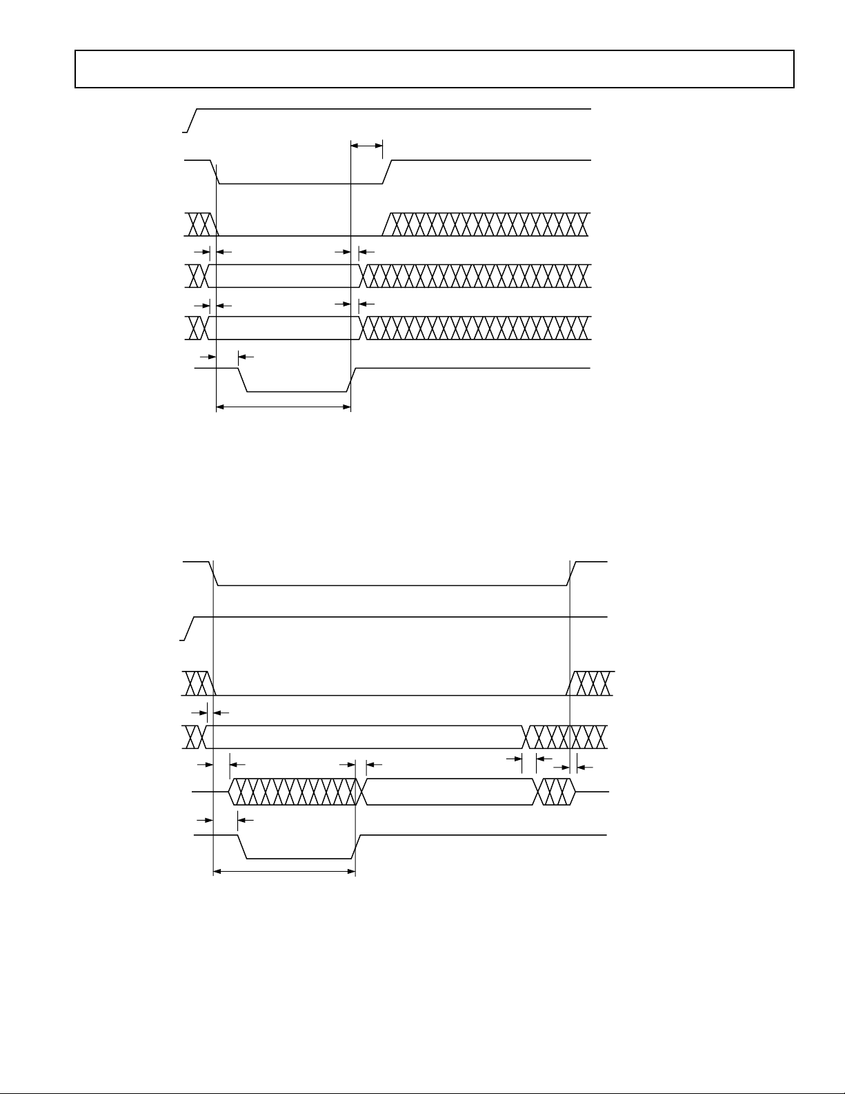
Figure 5. INM Microport Write Timing Requirements
RD (DS)
WR (R/W)
REV. 0
CS
t
SAM
A[2:0]
t
ZD
D[7:0]
t
DRDY
RDY
(DTACK)
1. t
ACCESS TIME DEPENDS ON THE ADDRESS ACCESSED. ACCESS TIME IS MEASURED FROM THE FE OF WR TO THE RE OF RDY.
ACC
FAST REQUIRES A MAXIMUM OF THREE CLK PERIODS AND APPLIES TO A[2:0] = 7, 6, 5, 3, 2, 1
2. t
ACC
MEDIUM REQUIRES A MAXIMUM OF FOUR CLK PERIODS AND APPLIES TO A[2:0] = 4 AND 0 IF THE ACCESS IS TO A CONTROL REGISTER
3. t
ACC
VERSUS A RAM REGISTER.
SLOW REQUIRES A MAXIMUM OF FIVE CLK PERIODS AND APPLIES TO A[2:0] = 0 WHEN ACCESSING RAM REGISTERS.
4. t
A
t
ACC
t
DD
VALID ADDRESS
VALID DATA
t
HA
t
ZD
Figure 6. INM Microport Read Timing Requirements
–5–
AD6622
DS (RD)
R/W (WR)
CS
A[2:0]
t
SAM
VALID ADDRESS
t
HAM
t
t
HDS
HRW
t
SAM
D[7:0]
DTACK
(RDY)
1. t
ACCESS TIME DEPENDS ON THE ADDRESS ACCESSED. ACCESS TIME IS MEASURED FROM THE FE OF DS TO THE FE OF DTACK.
ACC
FAST REQUIRES A MAXIMUM OF FOUR CLK PERIODS AND APPLIES TO A[2:0] = 7, 6, 3, 2, 1
2. t
ACC
MEDIUM REQUIRES A MAXIMUM OF FIVE CLK PERIODS AND APPLIES TO A[2:0] = 4, 5, AND 0 IF THE ACCESS IS TO A CONTROL REGISTER
3. t
ACC
VERSUS A RAM REGISTER.
SLOW REQUIRES A MAXIMUM OF SIX CLK PERIODS AND APPLIES TO A[2:0] = 0 WHEN ACCESSING RAM REGISTERS.
4. t
ACC
VALID DATA
t
ACC
t
HAM
t
DDTACK
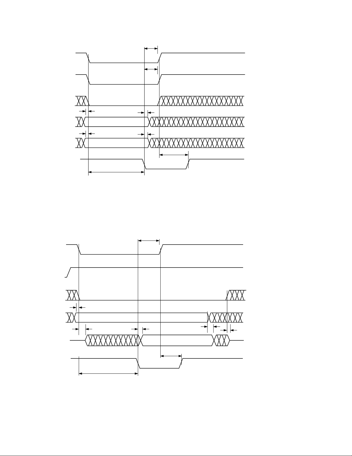
Figure 7. MNM Microport Write Timing Requirements
t
HDS
DS (RD)
R/W (WR)
CS
t
SAM
A[2:0]
t
ZD
D[7:0]
DTACK
(RDY)
1. t
ACCESS TIME DEPENDS ON THE ADDRESS ACCESSED. ACCESS TIME IS MEASURED FROM THE FE OF DS TO THE FE OF DTACK.
ACC
FAST REQUIRES A MAXIMUM OF FOUR CLK PERIODS AND APPLIES TO A[2:0] = 7, 6, 3, 2, 1
2. t
ACC
MEDIUM REQUIRES A MAXIMUM OF FIVE CLK PERIODS AND APPLIES TO A[2:0] = 4, 5, AND 0 IF THE ACCESS IS TO A CONTROL REGISTER
3. t
ACC
VERSUS A RAM REGISTER.
SLOW REQUIRES A MAXIMUM OF SIX CLK PERIODS AND APPLIES TO A[2:0] = 0 WHEN ACCESSING RAM REGISTERS.
4. t
ACC
t
ACC
t
DD
VALID ADDRESS
VALID DATA
t
DDTACK
t
HA
t
ZD
Figure 8. MNM Microport Read Timing Requirements
–6–
REV. 0
AD6622
WARNING!
ESD SENSITIVE DEVICE
ABSOLUTE MAXIMUM RATINGS*
Supply Voltage . . . . . . . . . . . . . . . . . . . . . . . .–0.3 V to +3.6 V
Input Voltage . . . . –0.3 V to VDD +0.3 V (Not 5 V Tolerant)
IN[17:0], QIN, OEN
Input Voltage . . . . . . . . . . . . . –0.3 V to +3.6 V (5 V Tolerant)
CLK, RESET, DS, R/W, MODE, A[2:0], D[7:0], SYNC, TRST,
TCK, TMS, TDI, SDINA, SDINB, SDINC, SDIND
Output Voltage Swing . . . . . . . . . . . . –0.3 V to VDD + 0.3 V
Load Capacitance . . . . . . . . . . . . . . . . . . . . . . . . . . . . 200 pF
Junction Temperature Under Bias . . . . . . . . . . . . . . . . . 125°C
Storage Temperature Range . . . . . . . . . . . . –65°C to +150°C
Lead Temperature (5 sec) . . . . . . . . . . . . . . . . . . . . . . . 280°C
*Stresses greater than those listed above may cause permanent damage to the
device. These are stress ratings only; functional operation of the devices at these
or any other conditions greater than those indicated in the operational sections of
this specification is not implied. Exposure to absolute maximum rating conditions
for extended periods may affect device reliability.
THERMAL CHARACTERISTICS
128-Lead MQFP:
= 33°C/W, No Airflow
θ
JA
θ
= 27°C/W, 200 LFPM Airflow
JA
θ
= 24°C/W, 400 LFPM Airflow
JA
= 5.5°C/W
θ
JC
Thermal measurements made in the horizontal position on a
2-layer board.
ORDERING GUIDE
EXPLANATION OF TEST LEVELS
I. 100% Production Tested.
II. 100% Production Tested at 25°C, and Sample Tested at
Specified Temperatures.
III. Sample Tested Only.
IV. Parameter Guaranteed by Design and Analysis.
V. Parameter is Typical Value Only.
VI. 100% Production Tested at 25°C, and Sample Tested at
Temperature Extremes.
Model Temperature Range Package Description Package Option
AD6622AS –40°C to +70°C (Ambient) 128-Lead MQFP (Metric Quad Flatpack) S-128A
AD6622S/PCB Evaluation Board with AD6622 and Software
CAUTION
ESD (electrostatic discharge) sensitive device. Electrostatic charges as high as 4000 V readily
accumulate on the human body and test equipment and can discharge without detection. Although
the AD6622 features proprietary ESD protection circuitry, permanent damage may occur on
devices subjected to high-energy electrostatic discharges. Therefore, proper ESD precautions are
recommended to avoid performance degradation or loss of functionality.
REV. 0
–7–
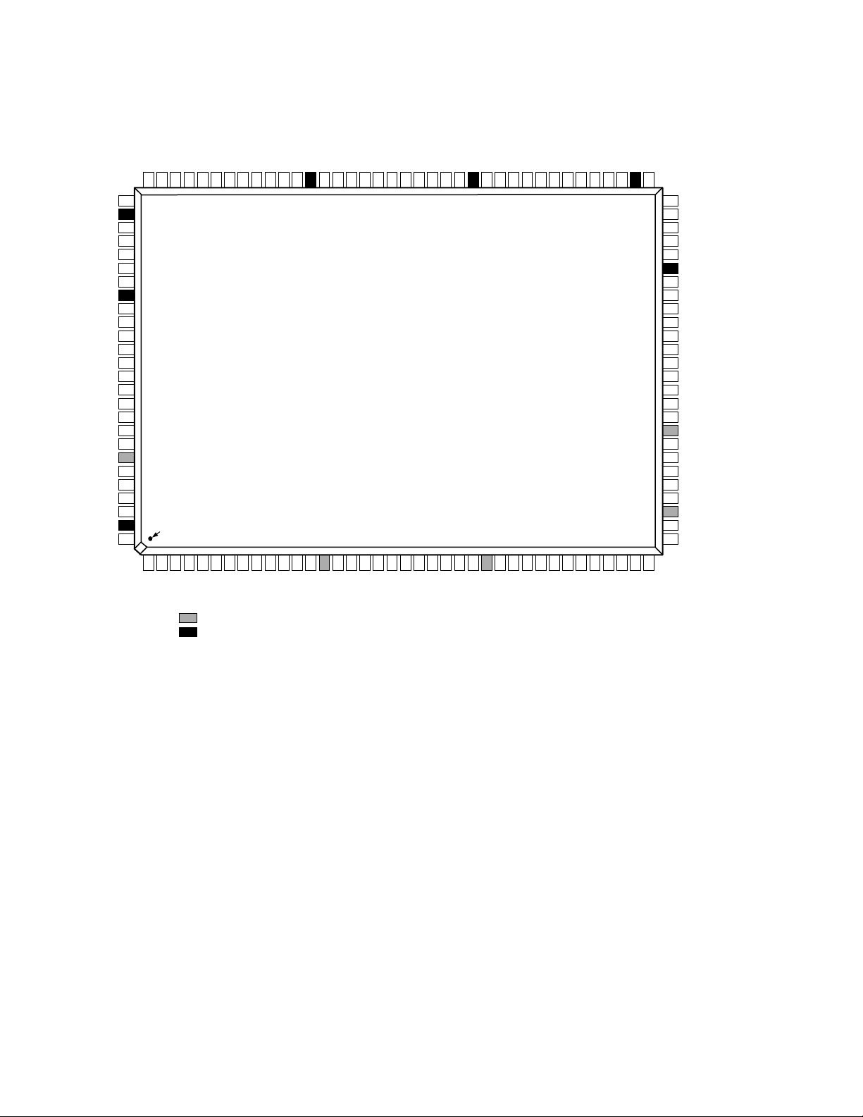
AD6622
GND
VDD
GND
TMS
TDO
TDI
SCLKA
VDD
SDFSA
SDINA
SCLKB
SDFSB
GND
GND
GND
SDINB
SCLKC
SDFSC
SDINC
VDD
SCLKD
SDFSD
SDIND
GND
VDD
GND
103
104
105
106
107
108
109
110
111
112
113
114
115
116
117
118
119
120
121
122
123
124
125
126
127
128
TCK
GND
101
102
PIN 1
IDENTIFIER
1
2
OEN
GND
GND
IN0
GND
GND
97
OUT0
95
769
8
OUT1
OUT2
IN1
94
GND
GND
TRST
98
99
100
5
3
4
GND
GND
GND
DENOTES I/O POWER PIN
DENOTES CORE POWER PIN
IN2
93
10
OUT3
IN3
92
11
OUT4
IN4
91
12
OUT5
PIN CONFIGURATION
VDD
IN5
IN6
IN7
IN8
GND
GND
GND
90
8889879686
83
82
84
AD6622
TOP VIEW
(Not to Scale)
13
OUT6
14
VDD
15
OUT7
16
OUT8
17
OUT9
18
19
GND
OUT10
20
GND
IN9
21
GND
IN10
81
22
OUT11
IN11
IN12
VDD
IN13
IN14
IN15
78
79
80
2326252827
OUT12
76
7785757374717269706768
24
VDD
OUT14
OUT15
OUT13
OUT16
IN16
GND
30
293231
QOUT
OUT17
GND
GND
IN17
GND
QIN
D7
GND
GND
CLK
VDD
66
37
3433363538
GND
GND
GNDD6GND
GND
65
64
GND
63
GND
62
SYNC
61
RESET
60
CS
59
VDD
A0
58
57
A1
56
A2
55
MODE
54
GND
GND
53
GND
52
51
R/W(WR)
50
DTACK(RDY)
49
DS(RD)
D0
48
47
VDD
46
D1
45
D2
44
D3
43
D4
42
GND
VDD
41
D5
40
GND
39
–8–
REV. 0

AD6622
PIN FUNCTION DESCRIPTIONS
Pin Number Name Type Description
1, 3–5, 9, 19–21, 31, 32, GND P Ground Connection
34–36, 38, 39, 42, 52–54,
63–65, 68, 69, 72, 73, 83–85,
95, 96, 98, 99, 102, 103,
105, 115–117, 126, 128
2 OEN I Active High Output Enable Pin (Actively Pulled Down If Not Connected)
(Not 5 V Tolerant)
27–29, 22–25, 15–18, 10–13, OUT[17:0] O/T Wideband Output Data
6–8
14, 26, 41, 47, 122 VDD P +3.0 V Supply (I/O Supply)
59, 66, 78, 90, 104, 110, 127 VDD P +3.0 V Supply (Core Supply)
30 QOUT O/T Indicates Q Output Data (Complex Output Mode)
33, 37, 40, 43–46, 48 D[7:0] I/O/T Microprocessor Interface Data
49 DS (RD) I INM Mode: Read Signal, MNM Mode: Data Strobe Signal
50 DTACK (RDY) O Acknowledgment of a Completed Transaction (Signals when µP Port
Is Ready for an Access) Open Drain, Must Be Pulled Up Externally
51 R/W (WR) I Read/Write Line (Write Signal)
55 MODE I Sets Microport Mode: MODE = 1, MNM Mode; MODE = 0, INM Mode
56–58 A[2:0] I Microprocessor Interface Address
60 CS I Chip Select, Enable the Chip for µP Access
61 RESET I Active Low Reset Pin (Actively Pulled Up If Not Connected)
62 SYNC I SYNC Signal for Synchronizing Multiple AD6622s (Actively Pulled
Down If Not Connected)
67 CLK I Input Clock (Actively Pulled Down If Not Connected)
70 QIN I Indicates Q Input Data (Complex Input Mode) (Actively Pulled Down
If Not Connected) (Not 5 V Tolerant)
71, 74–77, 79–82, 86–89, IN[17:0] I Wideband Input Data (Allows Cascade of Multiple AD6622 Chips In
91–94, 97 a System) (Actively Pulled Down If Not Connected) (Not 5 V Tolerant)
100 TRST I Test Reset Pin (Actively Pulled Up If Not Connected)
101 TCK I Test Clock Input (Actively Pulled Down If Not Connected)
106 TMS I Test Mode Select (Actively Pulled Up If Not Connected)
107 TDO O Test Data Output
108 TDI I Test Data Input (Actively Pulled Down If Not Connected)
109 SCLKA O Serial Clock Output Channel A
111 SDFSA O Serial Data Frame Sync Output Channel A
112 SDINA I Serial Data Input Channel A (Actively Pulled Down If Not Connected)
113 SCLKB O Serial Clock Output Channel B
114 SDFSB O Serial Data Frame Sync Output Channel B
118 SDINB I Serial Data Input Channel B (Actively Pulled Down If Not Connected)
119 SCLKC O Serial Clock Output Channel C
120 SDFSC O Serial Data Frame Sync Output Channel C
121 SDINC I Serial Data Input Channel C (Actively Pulled Down If Not Connected)
123 SCLKD O Serial Clock Output Channel D
124 SDFSD O Serial Data Frame Sync Output Channel D
125 SDIND I Serial Data Input Channel D (Actively Pulled Down If Not Connected)
REV. 0
–9–
 Loading...