Analog Devices AD6620 Datasheet
65 MSPS Digital Receive
a
FEATURES
High Input Sample Rate
65 MSPS Single Channel Real
32.5 MSPS Diversity Channel Real
32.5 MSPS Single Channel Complex
NCO Frequency Translation
Worst Spur Better than –100 dBc
Tuning Resolution Better than 0.02 Hz
2nd Order Cascaded Integrator Comb FIR Filter
Linear Phase, Fixed Coefficients
Programmable Decimation Rates: 2, 3 . . . 16
5th Order Cascaded Integrator Comb FIR Filter
Linear Phase, Fixed Coefficients
Programmable Decimation Rates: 1, 2, 3 . . . 32
Programmable Decimating RAM Coefficient FIR Filter
Up to 130 Million Taps per Second
256 20-Bit Programmable Coefficients
Programmable Decimation Rates: 1, 2, 3 . . . 32
Bidirectional Synchronization Circuitry
Phase Aligns NCOs
Synchronizes Data Output Clocks
Serial or Parallel Baseband Outputs
Pin Selectable Serial or Parallel
Serial Works with SHARC, ADSP-21xx, Most Other
DSPs
16-Bit Parallel Port, Interleaved I and Q Outputs
Two Separate Control and Configuration Ports
Generic P Port, Serial Port
3.3 V Optimized CMOS Process
JTAG Boundary Scan
GENERAL DESCRIPTION
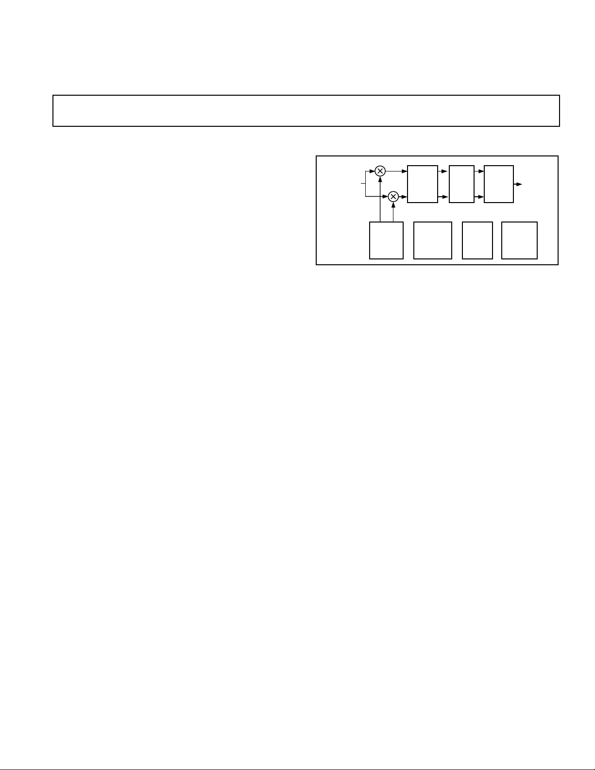
The AD6620 is a digital receiver with four cascaded signalprocessing elements: a frequency translator, two fixedcoefficient decimating filters, and a programmable coefficient
decimating filter. All inputs are 3.3 V LVCMOS compatible.
All outputs are LVCMOS and 5 V TTL compatible.
As ADCs achieve higher sampling rates and dynamic range, it
becomes increasingly attractive to accomplish the final IF stage
of a receiver in the digital domain. Digital IF Processing is less
expensive, easier to manufacture, more accurate, and more
flexible than a comparable highly selective analog stage.
The AD6620 diversity channel decimating receiver is designed
to bridge the gap between high speed ADCs and general purpose DSPs. The high resolution NCO allows a single carrier to
be selected from a high speed data stream. High dynamic range
decimation filters with a wide range of decimation rates allow
Signal Processor
AD6620
FUNCTIONAL BLOCK DIAGRAM
I
REAL,
DUAL REAL,
OR COMPLEX
INPUTS
COMPLEX
NCO
–SINCOS
Q
FILTERS
both narrowband and wideband carriers to be extracted. The
RAM-based architecture allows easy reconfiguration for multimode applications.
The decimating filters remove unwanted signals and noise from
the channel of interest. When the channel of interest occupies
less bandwidth than the input signal, this rejection of out-ofband noise is called “processing gain.” By using large decimation factors, this “processing gain” can improve the SNR of the
ADC by 36 dB or more. In addition, the programmable RAM
Coefficient filter allows antialiasing, matched filtering, and
static equalization functions to be combined in a single, costeffective filter.
The input port accepts a 16-bit Mantissa, a 3-bit Exponent,
and an A/B Select pin. These allow direct interfacing with the
AD6600, AD6640, AD9042 and most other high speed ADCs.
Three input modes are provided: Single Channel Real, Single
Channel Complex, and Diversity Channel Real.
When paired with an interleaved sampler such as the AD6600,
the AD6620 can process two data streams in the Diversity
Channel Real input mode. Each channel is processed with coherent frequency translation and output sample clocks. In addition, external synchronization pins are provided to facilitate
coherent frequency translation and output sample clocks among
several AD6620s. These features can ease the design of systems
with diversity antennas or antenna arrays.
Units are packaged in an 80-lead PQFP (plastic quad flatpack)
and specified to operate over the industrial temperature range
(–40°C to +85°C).
II
CIC
EXTERNAL
SYNC
CIRCUITRY
FIR
FILTER
QQ
JTAG
PORT
OUTPUT
FORMAT
OR SERIAL
SERIAL OR
PARALLEL
OUTPUTS
mP
CONTROL
REV. 0
Information furnished by Analog Devices is believed to be accurate and
reliable. However, no responsibility is assumed by Analog Devices for its
use, nor for any infringements of patents or other rights of third parties
which may result from its use. No license is granted by implication or
otherwise under any patent or patent rights of Analog Devices.
One Technology Way, P.O. Box 9106, Norwood, MA 02062-9106, U.S.A.
Tel: 781/329-4700 World Wide Web Site: http://www.analog.com
Fax: 781/326-8703 © Analog Devices, Inc., 1998

AD6620
TABLE OF CONTENTS
GENERAL DESCRIPTION . . . . . . . . . . . . . . . . . . . . . . . . . 1
ARCHITECTURE . . . . . . . . . . . . . . . . . . . . . . . . . . . . . . . . 2
SPECIFICATIONS/TIMING . . . . . . . . . . . . . . . . . . . . . . . 4
ABSOLUTE MAXIMUM RATINGS . . . . . . . . . . . . . . . . 11
EXPLANATION OF TEST LEVELS . . . . . . . . . . . . . . . . 11
ORDERING GUIDE . . . . . . . . . . . . . . . . . . . . . . . . . . . . . 11
PIN FUNCTION DESCRIPTIONS . . . . . . . . . . . . . . . . . 12
PIN CONFIGURATIONS . . . . . . . . . . . . . . . . . . . . . . . . . 13
INPUT DATA PORT . . . . . . . . . . . . . . . . . . . . . . . . . . . . . 15
OUTPUT DATA PORT . . . . . . . . . . . . . . . . . . . . . . . . . . . 18
FREQUENCY TRANSLATOR . . . . . . . . . . . . . . . . . . . . . 20
2ND ORDER CASCADED INTEGRATOR
COMB FILTER . . . . . . . . . . . . . . . . . . . . . . . . . . . . . . . 21
5TH ORDER CASCADED INTEGRATOR
COMB FILTER . . . . . . . . . . . . . . . . . . . . . . . . . . . . . . . 23
RAM COEFFICIENT FILTER . . . . . . . . . . . . . . . . . . . . . 25
CONTROL REGISTERS AND ON-CHIP RAM . . . . . . . 27
PROGRAMMING THE AD6620 . . . . . . . . . . . . . . . . . . . 29
MICROPORT CONTROL . . . . . . . . . . . . . . . . . . . . . . . . 31
SERIAL PORT CONTROL . . . . . . . . . . . . . . . . . . . . . . . . 34
JTAG BOUNDARY SCAN . . . . . . . . . . . . . . . . . . . . . . . . 36
APPLICATIONS . . . . . . . . . . . . . . . . . . . . . . . . . . . . . . . . 37
OUTLINE DIMENSIONS . . . . . . . . . . . . . . . . . . . . . . . . . 43
ARCHITECTURE
As shown in Figure 1, the AD6620 has four main signal processing stages: a Frequency Translator, two Cascaded Integrator
Comb FIR Filters (CIC2, CIC5), and a RAM Coefficient FIR
Filter (RCF). Multiple modes are supported for clocking data
into and out of the chip. Programming and control is accomplished via serial and microprocessor interfaces.
Input data to the chip may be real or complex. If the input data
is real, it may be clocked in as a single channel or interleaved
with a second channel. The two-channel input mode, called
Diversity Channel Real, is typically used in diversity receiver
applications. Input data is clocked in 16-bit parallel words,
IN[15:0]. This word may be combined with exponent input bits
EXP[2:0] when the AD6620 is being driven by floating-point or
gain-ranging analog-to-digital converters such as the AD6600.
Frequency translation is accomplished with a 32-bit complex
Numerically Controlled Oscillator (NCO). Real data entering
this stage is separated into in-phase (I) and quadrature (Q)
components. This stage translates the input signal from a digital
intermediate frequency (IF) to baseband. Phase and amplitude
dither may be enabled on-chip to improve spurious performance
of the NCO. A phase offset word is available to create a known
phase relationship between multiple AD6620s.
Following frequency translation is a fixed coefficient, high speed
decimating filter that reduces the sample rate by a programmable ratio between 2 and 16. This is a second order, cascaded
integrator comb FIR filter shown as CIC2 in Figure 1. (Note:
Decimation of 1 in CIC2 requires 2× or greater clock into
AD6620). The data rate into this stage equals the input data
rate, f
the decimation factor, M
. The data rate out of CIC2, f
SAMP
CIC2
.
, is determined by
SAMP2
EXP[2:0]
IN[15:0]
FREQUENCY
TRANSLATOR
16
PHASE
OFFSET
CLK
A/B
RESET
SYNC NCO
SYNC CIC
RCF
SYNC
3
16
COMPLEX
NCO
INPUT
DATA
I
Q
TIMING
SYNC
I/O
RCF
I-RAM
INTERLEAVE
MODE
MULTI-
PLEXER
f
SAMP5
SCALING, S
PAR/SER
PARALLEL
CIC5
DS
(R/D)
M
OUTPUT
SCALE
FACTOR
DTACKCS
(RDY)
CICS
3
18
EXP
SCALING
18
EXPLNV,
EXPOFF
f
SAMP
FIXED OR WITH EXPONENT
TRST
CIC2
SCALING
NCO FREQUENCY
PHASE OFFSET
DITHER
SYNC MASK
INPUT MODE
REAL, DUAL, COMPLEX
SYNC M/S
JTAG
TCK TMS TDI TDO
M
MULTI-
PLEXER
CICS
CIC2, CIC5
DECIMATE FACTORS
SCALE FACTORS
CONTROL REGISTERS
MICROPORT AND
SERIAL ACCESS
MICROPROCESSOR INTERFACE
D[7:0] A[2:0]
SCALING
f
SAMP2
RCF COEFFICIENTS
NUMBER OF TAPS
DECIMATE FACTOR
ADDRESS OFFSET
R/W
(W/R)
DE-
INTERLEAVE
23
23
OUTPUT
OUT
16
256 3 20
C-RAM
256 3 20
Q-RAM
256 3 20
MULTIPLEXER
SERIAL
PARALLEL
OUTPUTS
AND
SERIAL I/O
DV
I/Q
A/B
M
OUT
OUT
OUT
RCF
16
OUT[15:0]
SCLK
SDI
SDO
SDFS
SDFE
SBM
WL[1:0]
AD
SDIV[3:0]
Figure 1. Block Diagram
–2–
REV. 0
AD6620
Following CIC2 is the second fixed-coefficient decimating filter.
This filter, CIC5, further reduces the sample rate by a programmable ratio from 1 to 32. The data rate out of CIC5, f
determined by the decimation factors of M
CIC5
and M
SAMP5
CIC2
, is
.
Each CIC stage is a FIR filter whose response is defined by the
decimation rate. The purpose of these filters is to reduce the
data rate of the incoming signal so that the final filter stage, a
FIR RAM coefficient sum-of-products filter (RCF), can calculate more taps per output. As shown in Figure 1, on-chip multiplexers allow both CIC filters to be bypassed if a multirate clock
is used.
The fourth stage is a sum-of-products FIR filter with programmable 20-bit coefficients, and decimation rates programmable
from 1 to 32. The RAM Coefficient FIR Filter (RCF in Figure
1) can handle a maximum of 256 taps.
WIDEBAND INPUT SPECTRUM
SIGNAL OF INTEREST "IMAGE"
C'
D'
–fS/2 –3fS/8 –5fS/16 –fS/4 –3fS/16 –fS/8 –fS /16
B'
A'
DC
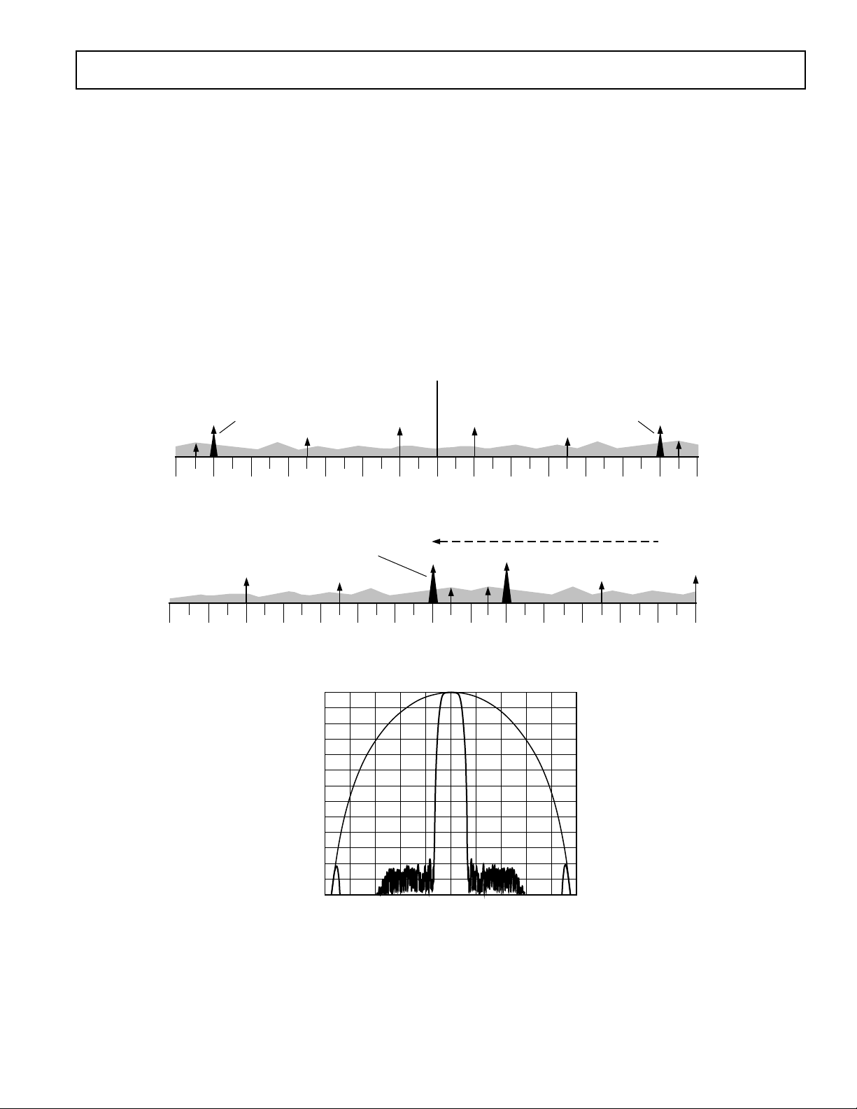
Figure 2a. Wideband Input Spectrum (e.g., 30 MHz from High Speed ADC)
The overall filter response for the AD6620 is the composite of
all three cascaded decimating filters: CIC2, CIC5, and RCF.
Each successive filter stage is capable of narrower transition
bandwidths but requires a greater number of CLK cycles to
calculate the output. More decimation in the first filter stage will
minimize overall power consumption. Data comes out via a
parallel port or a serial interface.
Figure 2 illustrates the basic function of the AD6620: to select
and filter a single channel from a wide input spectrum. The
frequency translator “tunes” the desired carrier to baseband.
CIC2 and CIC5 have fixed order responses; the RCF filter
provides the sharp transitions. More detail is provided in later
sections of the data sheet.
2 TO f
(–f
samp/
A
fS/16 fS/8 3fS/16 fS/4 5fS/16 fS/23fS/8
B
2)
samp/
SIGNAL OF
INTEREST
C
D
NCO "TUNES" SIGNAL TO BASEBAND
AFTER FREQUENCY TRANSLATION
A
–fS/2 –3fS/8 –5fS/16 –fS/4 –3fS/16 –fS/8 –fS/16 DC fS/16 fS/8 3fS/16 fS/4 5fS/16 fS/23fS/8
B
C
D
C'
D'
B'
Figure 2b. Frequency Translation (e.g. Single 1 MHz Channel Tuned to Baseband)
CIC2, CIC5, AND RCF
FREQUENCY
dBc
–100
–110
–120
–130
0
–10
–20
–30
–40
–50
–60
–70
–80
–90
Figure 2c. Baseband Signal is Decimated and Filtered by CIC2, CIC5, RCF
A'
–3–REV. 0

AD6620–SPECIFICATIONS
RECOMMENDED OPERATING CONDITIONS
Test AD6620AS
Parameter Level Min Typ Max Units
VDD I 3.0 3.3 3.6 V
T
AMBIENT
ELECTRICAL CHARACTERISTICS
Parameter (Conditions) Temp Level Min Typ Max Units
LOGIC INPUTS
Logic Compatibility Full 3.3 V CMOS
Logic “1” Voltage Full I 2.0 VDD + 0.3 V
Logic “0” Voltage Full I –0.3 0.8 V
Logic “1” Current Full I 1 10 µA
Logic “0” Current Full I 1 10 µA
Input Capacitance +25°CV 4 pF
LOGIC OUTPUTS
Logic Compatibility Full 3.3 V CMOS/TTL
Logic “1” Voltage (I
Logic “0” Voltage (IOL = 1.0 mA) Full I 0.2 0.4 V
IDD SUPPLY CURRENT
CLK = 20 MHz
CLK = 65 MHz
Reset Mode
POWER DISSIPATION
CLK = 20 MHz
CLK = 65 MHz
Reset Mode
NOTES
1
Input-Only Pins: CLK, RESET, IN[15:0], EXP[2:0], A/B, PAR/SEL.
2
Bidirectional Pins: SYNC_NCO, SYNC_CIC, SYNC_RCF.
3
Microinterface Input Pins: DS (RD), R/W (WR), CS.
4
Microinterface Bidirectional Pins: A[2:0], D[7:0].
5
JTAG Input Pins: TRST, TCK, TMS, TDI.
6
Serial Mode Input Pins: SDI, SBM, WL[1:0], AD, SDIV[3:0].
7
Serial Mode Bidirectional Pins: SCLK, SDFS.
8
Output Pins: OUT[15:0], DV
9
Microinterface Output Pins: DTACK (RDY).
10
JTAG Output Pins: TDO.
11
Serial Mode Output Pins: SDO, SDFE.
12
Conditions for IDD @ 20 MHz. M
13
Conditions for IDD @ 65 MHz. M
14
Conditions for IDD in Reset (RESET = 0).
Specifications subject to change without notice.
1, 2, 3, 4, 5, 6, 7
2, 4, 7, 8, 9, 10, 11
12
13
14
12
13
14
(NOT 5 V TOLERANT)
= 0.5 mA) Full I 2.4 VDD – 0.2 V
OH
Full V 52 mA
Full I 167 227 mA
Full I 1 mA
Full V 170 mW
Full I 550 750 mW
Full I 3.3 mW
, A/B
, I/Q
OUT
CIC2
CIC2
OUT
= 2, M
= 2, M
OUT
CIC5
CIC5
.
= 2, M
= 2, M
= 1, 4 RCF taps of alternating positive and negative full scale.
RCF
= 1, 4 RCF taps of alternating positive and negative full scale.
RCF
IV –40 +25 +85 °C
Test AD6620AS
–4–
REV. 0

AD6620
TIMING CHARACTERISTICS
(C
= 40 pF All Outputs)
LOAD
Test AD6620AS
Parameter (Conditions) Temp Level Min Typ Max Units
CLK Timing Requirements:
t
CLK
t
CLKL
t
CLKH
CLK Period Full I 15.4 ns
CLK Width Low Full IV 7.0 0.5 × t
CLK Width High Full IV 7.0 0.5 × t
CLK
CLK
ns
ns
Reset Timing Requirements:
t
RESL
RESET Width Low Full I 30.0 ns
Input Data Timing Requirements:
t
SI
t
HI
Input1 to CLK Setup Time Full IV –1.0 ns
Input1 to CLK Hold Time Full IV 6.5 ns
Parallel Output Switching Characteristics:
t
DPR
t
DPF
t
DPR
t
DPF
t
DPR
t
DPF
t
DPR
t
DPF
CLK to OUT[15:0] Rise Delay Full IV 8.0 19.5 ns
CLK to OUT[15:0] Fall Delay Full IV 7.5 19.5 ns
CLK to DV
CLK to DV
CLK to I
CLK to I
CLK to A
CLK to A
Rise Delay Full IV 6.5 19.0 ns
OUT
Fall Delay Full IV 5.5 11.5 ns
OUT
Rise Delay Full IV 7.0 19.5 ns
QOUT
Fall Delay Full IV 6.0 13.5 ns
QOUT
Rise Delay Full IV 7.0 19.5 ns
BOUT
Fall Delay Full IV 5.5 13.5 ns
BOUT
SYNC Timing Requirements:
t
SY
t
HY
SYNC2 to CLK Setup Time Full IV –1.0 ns
SYNC2 to CLK Hold Time Full IV 6.5 ns
SYNC Switching Characteristics:
t
DY
CLK to SYNC3 Delay Time Full V 7.0 23.5 ns
Serial Input Timing:
t
SSI
t
HSI
t
HSRF
t
SSF
t
HSF
SDI to SCLKt Setup Time Full IV 1.0 ns
SDI to SCLKt Hold Time Full IV 2.0 ns
SDFS to SCLKu Hold Time Full IV 4.0 ns
SDFS to SCLKt Setup Time
SDFS to SCLKt Hold Time
4
4
Full IV 1.0 ns
Full IV 2.0 ns
Serial Frame Output Timing:
t
DSE
t
SDFEH
t
DSO
SCLK Switching Characteristics, SBM = “1”:
t
SCLK
t
SCLKL
t
SCLKH
t
SCLKD
SCLKu to SDFE Delay Time Full IV 3.5 11.0 ns
SDFE Width High Full V t
SCLK
ns
SCLKu to SDO Delay Time Full IV 4.5 11.0 ns
SCLK Period
SCLK Width Low Full V 0.5 × t
SCLK Width High Full V 0.5 × t
3
Full I 2 × t
CLK
SCLK
SCLK
ns
ns
ns
CLK to SCLK Delay Time Full V 6.5 13.0 ns
Serial Frame Timing, SBM = “1”:
t
DSF
t
SDFSH
SCLKu to SDFS Delay Time Full IV 1.0 4.0 ns
SDFS Width High Full V t
SCLK
ns
SCLK Timing Requirements, SBM = “0”:
t
SCLK
t
SCLKL
t
SCLKH
NOTES
1
Specification pertains to: IN[15:0], EXP[2:0], A/B.
2
Specification pertains to: SYNC_NCO, SYNC_CIC, SYNC_RCF.
3
SCLK period will be ≥ 2 × t
4
SDFS setup and hold time must be met, even when configured as outputs, since internally the signal is sampled at the pad.
Specifications subject to change without notice.
SCLK Period Full I 15.4 ns
SCLK Width Low Full IV 0.4 × t
SCLK Width High Full IV 0.4 × t
when AD6620 is Serial Bus Master (SBM = 1) depending on the SDIV word.
CLK
SCLK
SCLK
0.5 × t
0.5 × t
SCLK
SCLK
ns
ns
–5–REV. 0

AD6620
TIMING CHARACTERISTICS
(C
= 40 pF All Outputs)
LOAD
Test AD6620AS
Parameter (Conditions) Temp Level Min Typ Max Units
MICROPROCESSOR PORT, MODE = 0
MODE 0 Input Timing Requirements:
t
SC
t
HC
t
HA
t
ZR
t
ZD
t
SAM
Control1 to CLK Setup Time Full IV 3.0 ns
Control1 to CLK Hold Time Full IV 5.0 ns
Address2 to CLK Hold Time Full IV 3.0 ns
CS to Data Enabled Time Full IV 5.0 ns
CS to Data Disabled Time Full IV 5.0 ns
CS to Address/Data Setup Time Full IV 0.0 ns
MODE 0 Read Switching Characteristics:
t
DD
t
RDY
CLK to Data Valid Time Full I 10.0 15.0 30.0 ns
RD to RDY Time Full IV 4.0 19.5 ns
MODE 0 Write Timing Requirements:
t
SC
t
HC
t
HM
t
HA
t
SAM
Control1 to CLK Setup Time Full IV 3.0 ns
Control1 to CLK Hold Time Full IV 5.0 ns
Micro Data3 to CLK Hold Time Full IV 3.0 ns
Address2 to CLK Hold Time Full IV 3.0 ns
Address/Data Setup Time to CS Full IV 0.0 ns
MODE 0 Write Switching Characteristics:
t
RDY
RD to RDY Time Full IV 4.0 19.5 ns
MICROPROCESSOR PORT, MODE = 1
MODE1 Input Timing Requirements:
t
SC
t
HC
t
HA
t
ZR
t
ZD
t
SAM
Control1 to CLK Setup Time Full IV 3.0 ns
Control1 to CLK Hold Time Full IV 5.0 ns
Address2 to CLK Hold Time Full IV 3.0 ns
CS to Data Enabled Time Full IV 5.0 ns
CS to Data Disabled Time Full IV 5.0 ns
Address/Data Setup Time to CS Full IV 0.0 ns
MODE1 Read Switching Characteristics:
t
DD
t
DTACK
CLK to Data Valid Time Full I 10.0 30.0 ns
CLK to DTACK Time Full V 5.5 15.5 ns
MODE1 Write Timing Requirements:
t
SC
t
HC
t
HM
t
HA
t
SAM
Control1 to CLK Setup Time Full IV 0.0 ns
Control1 to CLK Hold Time Full IV 5.0 ns
Micro Data3 to CLK Hold Time Full IV 6.5 ns
Address2 to CLK Hold Time Full IV 3.0 ns
Address/Data Setup Time to CS Full IV 0.0 ns
MODE1 Write Switching Characteristics:
t
DTACK
NOTES
1
Specification pertains to: R/W (WR), DS (RD), CS.
2
Specification pertains to: A[2:0].
3
Specification pertains to: D[7:0].
Specifications subject to change without notice.
CLK to DTACK Time Full V 5.5 15.5 ns
–6–
REV. 0
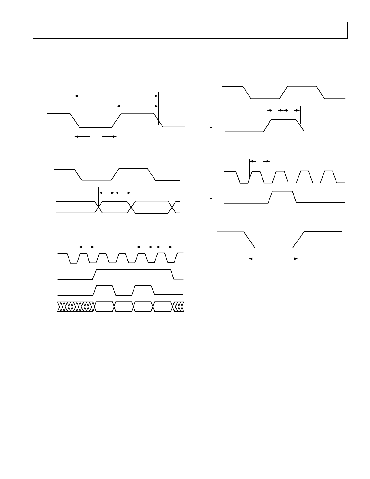
TIMING DIAGRAMS
AD6620
CLK, INPUTS, PARALLEL OUTPUTS
RESET with PAR/SER = “1” establishes Parallel Outputs active.
t
CLK
t
CLKH
CLK
t
CLKL
Figure 3. CLK Timing Requirements
CLK
t
IN[15:0]
EXP[2:0]
A/B
t
SI
HI
DATA
Figure 4. Input Data Timing Requirements
t
DPR
t
DPF
t
DPF
SYNC PULSES: SLAVE OR MASTER
CLK
t
t
HY
SY
NCO
SYNC
SYNC
CIC
RCF
SYNC
Figure 6. SYNC Slave Timing Requirements
t
DY
CLK
NCO
SYNC
CIC
SYNC
RCF
SYNC
Figure 7. SYNC Master Delay
RESET
CLK
DV
OUT
I/Q
OUT
OUT[15:0]
VALID OUTPUT DATA
I
I
A
Q
Q
I
I
A
B
Figure 5. Parallel Output Switching Characteristics
t
RESL
Figure 8. Reset Timing Requirements
Q
Q
B
–7–REV. 0
AD6620
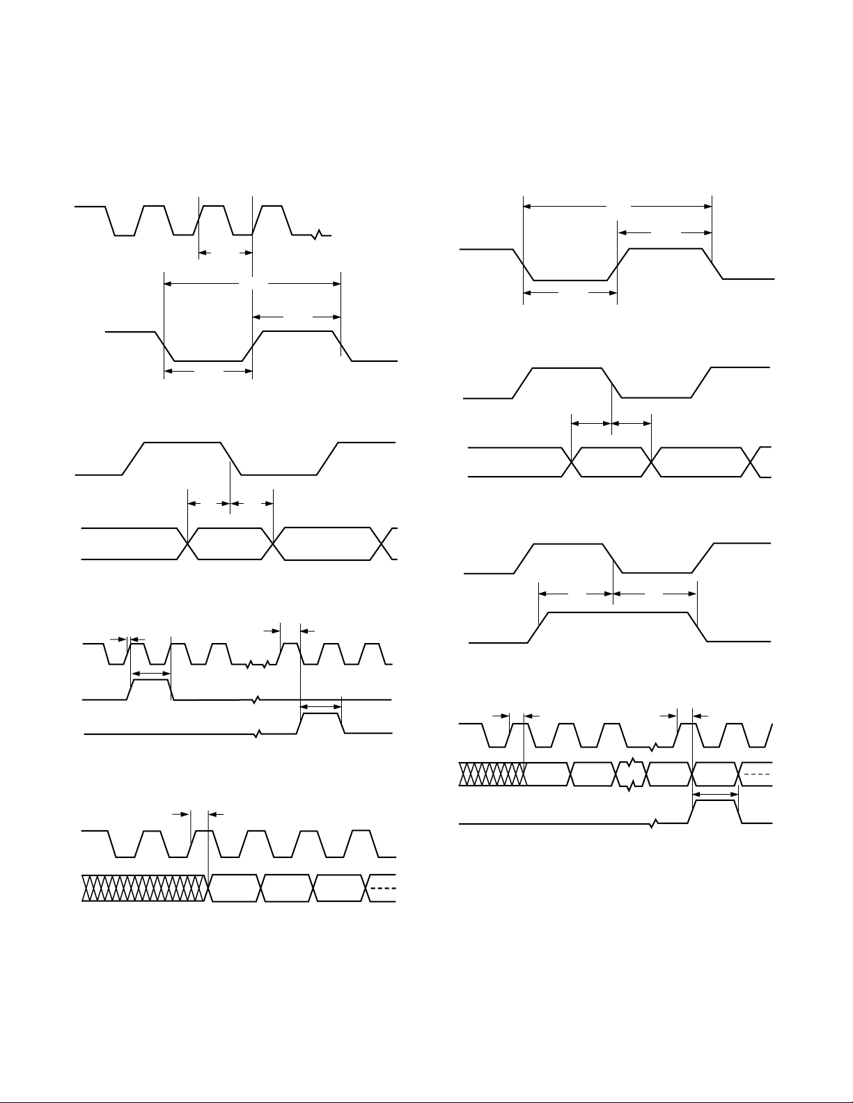
SERIAL PORT: BUS MASTER
RESET with PAR/SER = “0” establishes Serial Port active.
SBM = “1” puts AD6620 in Serial Bus Master mode SCLK is
output; SDFS is output.
CLK
t
SCLKD
t
SCLK
t
SCLKH
SCLK
t
SCLKL
Figure 9. SCLK Switching Characteristics
SCLK
t
SSI
t
HSI
SERIAL PORT: CASCADE MODE
RESET with PAR/SER = “0” establishes Serial Port active.
SBM = “0” puts AD6620 in Serial Port Cascade mode, SCLK
is input; SDFS is input.
t
SCLK
t
SCLKH
SCLK
t
SCLKL
Figure 13. SCLK Timing Requirements
SCLK
t
t
SSI
HSI
SDI
DATA
Figure 14. Serial Input Data Timing Requirements
DATASDI
Figure 10. Serial Input Data Timing Requirements
t
SCLK
SDFS
SDFE
DSF
t
SDFSH
t
DSE
t
SDFEH
Figure 11. Serial Frame Switching Characteristics
t
DSO
SCLK
SDO
I
15
I
14
I
13
Figure 12. Serial Output Data Switching Characteristics
SCLK
SDFS
t
SSF
t
HSF
Figure 15. SDFS Timing Requirements
t
DSE
Q
1
SCLK
SDO
SDFE
t
I
DSO
15
I
14
Figure 16. SDO, SDFE Switching Characteristics
Q
0
t
SDFEH
–8–
REV. 0
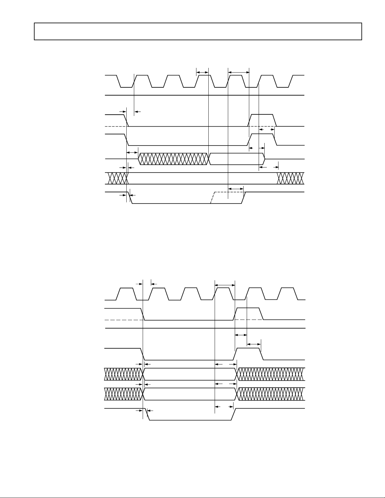
MICROPORT MODE0, READ
Timing is synchronous to CLK; MODE = 0.
AD6620
t
DD
1
CLK
2
WR
2
RD
3
CS
t
D[7:0]
A[2:0]
1
RDY
NOTES:
1
RDY IS DRIVEN LOW ASYNCHRONOUSLY BY RD AND CS GOING LOW AND RETURNS HIGH ON THE RISING EDGE
OF CLK "N+3" FOR INTERNAL ACCESS (A[2:0] = 000), CLK "N+2" OTHERWISE.
2
THE SIGNAL, WR, MAY REMAIN HIGH AND RD MAY REMAIN LOW TO CONTINUE READ MODE.
3
CS MUST RETURN TO HIGH STATE AND BE SAMPLED BY CLK (N+4 SHOWN) TO COMPLETE READ.
ZR
t
SAM
N N+1 N+2 N+3 N+4 N
t
SC
ADDRESS VALID
t
RDY
t
HC
DATA VALID
t
RDY
t
HC
t
ZD
t
HA
Figure 17. MODE0 Read Timing Requirements and Switching Characteristics
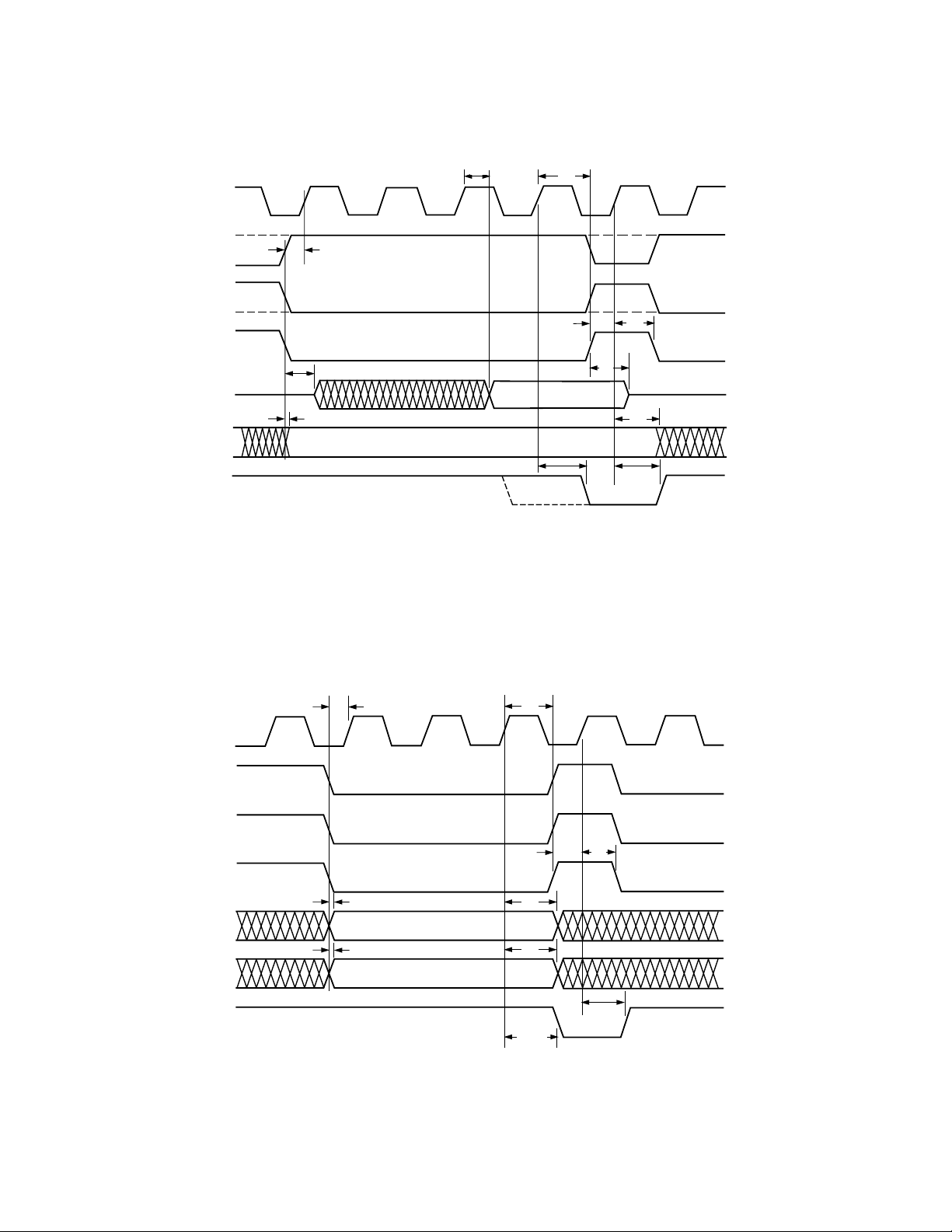
MICROPORT MODE0, WRITE
Timing is synchronous to CLK; MODE = 0.
t
SC
1
CLK
2
WR
2
RD
3
CS
t
SAM
D[7:0]
t
SAM
A[2:0]
RDY
NOTES:
1
RDY IS DRIVEN LOW ASYNCHRONOUSLY BY WR AND CS GOING LOW AND RETURNS HIGH ON THE
RISING EDGE OF CLK "N+2".
2
THESE SIGNALS (R/W AND DS) MAY REMAIN IN LOW STATE TO CONTINUE WRITING DATA.
3
CS MUST RETURN TO HIGH STATE AND BE SAMPLED BY CLK (N+3 SHOWN) TO COMPLETE WRITE.
* THE NEXT WRITE MAY BE INITIATED ON CLK, N*.
t
HC
N N+1 N+2 N+3 N*
t
SC
t
HC
t
HM
DATA VALID
t
HA
ADDRESS VALID
t
t
RDY
RDY
Figure 18. MODE0 Write Timing Requirements and Switching Characteristics
–9–REV. 0
AD6620
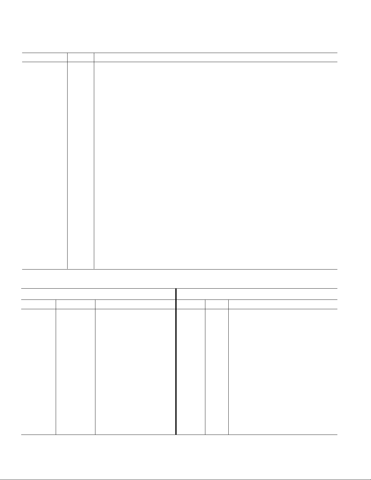
MICROPORT MODE1, READ
Timing is synchronous to CLK; MODE = 1.
CLK
1
N
t
N+1 N+2
DD
N+3
t
HC
N+4
N
2
R/W
2
DS
3
CS
D[7:0]
A[2:0]
DTACK
NOTES:
1
DTACK IS DRIVEN LOW ON THE RISING EDGE OF CLK "N+3" FOR INTERNAL ACCESS (A[2:0] = 000),
CLK "N=2" OTHERWISE.
2
THE SIGNAL, R/W MAY REMAIN HIGH AND DS MAY REMAIN LOW TO CONTINUE READ MODE.
3
CS MUST RETURN TO HIGH STATE AND BE SAMPLED BY CLK (N+4 SHOWN) TO COMPLETE ACCESS
AND FORCE DTACK HIGH.
t
SC
t
ZR
t
SAM
Figure 19. MODE1 Read Timing Requirements and Switching Characteristics
MICROPORT MODE1, WRITE
Timing is synchronous to CLK; MODE = 1.
ADDRESS VALID
t
DTACK
DATA VALID
t
t
SC
HC
t
ZD
t
HA
t
DTACK
CLK
R/W
DS
CS
D[7:0]
A[2:0]
DTACK
t
SC
1
2
2
3
t
SAM
t
SAM
NOTES:
1
ON RISING EDGE OF "N+3" CLK, DTACK IS DRIVEN LOW.
2
THESE SIGNALS (R/W AND DS) MAY REMAIN IN LOW STATE TO CONTINUE WRITING DATA.
3
CS MUST RETURN TO HIGH STATE AND BE SAMPLED BY CLK (N+3 SHOWN) TO COMPLETE WRITE
AND FORCE DTACK HIGH.
* THE NEXT WRITE MAY BE INITIATED ON CLK, N*.
N
N+1 N+2
DATA VALID
ADDRESS VALID
t
t
t
t
DTACK
HC
N+3
t
t
HC
SC
HM
HA
t
DTACK
N*
Figure 20. MODE1 Write Timing Requirements and Switching Characteristics
–10–
REV. 0

AD6620
ABSOLUTE MAXIMUM RATINGS*
Supply Voltage . . . . . . . . . . . . . . . . . . . . . . . . –0.3 V to +4.5 V
Input Voltage . . . . –0.3 V to VDD + 0.3 V (Not 5 V Tolerant)
Output Voltage Swing . . . . . . . . . . . . –0.3 V to VDD + 0.3 V
Load Capacitance . . . . . . . . . . . . . . . . . . . . . . . . . . . . 200 pF
Junction Temperature Under Bias . . . . . . . . . . . . . . . .+130°C
Storage Temperature Range . . . . . . . . . . . . –65°C to +150°C
Lead Temperature (5 sec) . . . . . . . . . . . . . . . . . . . . . .+280°C
*Stresses greater than those listed above may cause permanent damage to the
device. These are stress ratings only; functional operation of the device at these
or any other conditions greater than those indicated in the operational sections of
this specification is not implied. Exposure to absolute maximum rating conditions
for extended periods may affect device reliability.
Thermal Characteristics
EXPLANATION OF TEST LEVELS
I. 100% Production Tested.
II. 100% Production Tested at +25°C, and Sampled Tested at
Specified Temperatures.
III. Sample Tested Only.
IV. Parameter Guaranteed by Design and Analysis.
V. Parameter is Typical Value Only.
VI. 100% Production Tested at +25°C, and Sampled Tested at
Temperature Extremes.
80-Lead Plastic Quad Flatpack:
θ
= 44°C/Watt
JA
ORDERING GUIDE
Model Temperature Range Package Description Option
AD6620AS –40°C to +85°C (Ambient) 80-Lead PQFP (Plastic Quad Flatpack) S-80A
AD6620S/PCB Evaluation Board with AD6620AS and Software
CAUTION
ESD (electrostatic discharge) sensitive device. Electrostatic charges as high as 4000 V readily
accumulate on the human body and test equipment and can discharge without detection.
Although the AD6620 features proprietary ESD protection circuitry, permanent damage may
occur on devices subjected to high energy electrostatic discharges. Therefore, proper ESD
precautions are recommended to avoid performance degradation or loss of functionality.
Package
WARNING!
ESD SENSITIVE DEVICE
–11–REV. 0
AD6620
PIN FUNCTION DESCRIPTIONS
Name Type Description
VDD P +3.3 V Supply
VSS G Ground
CLK I Input Clock
RESET I Active Low Reset Pin
IN[15:0] I Input Data (Mantissa)
EXP[2:0] I Input Data (Exponent)
A/B I Channel (A/B) Select
SYNC_NCO I/O Sync Signal for NCO
SYNC_CIC I/O Sync Signal for CIC Stages
SYNC_RCF I/O Sync Signal for RCF
MODE I Sets Microport Mode: Mode 1, (MODE = 1), Mode 0, (MODE = 0)
A[2:0] I Microprocessor Interface Address
D[7.0] I/O/T Microprocessor Interface Data
DS or RD I Mode 1: Data Strobe Line, Mode 0: Read Signal
R/W or WR I Read/Write Line (Write Signal)
CS I Chip Select, Enables the Chip for µP Access
DTACK or RDY O Acknowledgment of a Completed Transaction (Signals when µP Port Is Ready for an Access)
PAR/SER I Parallel/Serial Control Select (PAR = 1, SER = 0)
DV
OUT
A/B
OUT
I/Q
OUT
TRST I Test Reset Pin
TCK I Test Clock Input
TMS I Test Mode Select Input
TDI I Test Data Input
TDO I Test Data Output
Pin Types: I = Input, O = Output, P = Power Supply, G = Ground, T = Three-state.
O Data Valid Pin for the Parallel Output Data
O Signals to Which Channel the Output Belongs to (A = 1, B = 0)
O Signals Whether I or Q Data Is Present (I = 1, Q = 0)
SHARED PINS
Parallel Outputs (PAR/SER = 1 at RESET) Serial Port (PAR/SER = 0 at RESET)
Name Type Description Name Type Description
OUT15 O Parallel Output Data SCLK I/O Serial Clock Input (SBM =0)
Serial Clock Output (SBM = 1)
OUT14 O Parallel Output Data SDI I Serial Data Input
OUT13 O Parallel Output Data SDO O/T Serial Data Output
OUT12 O Parallel Output Data SDFS I/O Serial Data Frame Sync Input (SBM = 0)
Serial Data Frame Sync Output (SBM = 1)
OUT11 O Parallel Output Data SDFE O Serial Data Frame End
OUT10 O Parallel Output Data SBM I Serial Bus Master (Master = 1, Cascade = 0)
OUT9 O Parallel Output Data WL1 I Serial Port Word Length, Bit 1
OUT8 O Parallel Output Data WL0 I Serial Port Word Length, Bit 0
OUT7 O Parallel Output Data AD I Append Data
OUT[6:4] O Parallel Output Data NC NC Unused, Do Not Connect
OUT3 O Parallel Output Data SDIV3 I SCLK Divide Value, Bit 3
OUT2 O Parallel Output Data SDIV2 I SCLK Divide Value, Bit 2
OUT1 O Parallel Output Data SDIV1 I SCLK Divide Value, Bit 1
OUT0 O Parallel Output Data (LSB) SDIV0 I SCLK Divide Value, Bit 0
Pin Types: I = Input, O = Output, P = Power Supply, G = Ground, T = Three-state.
–12–
REV. 0

PIN CONFIGURATIONS
Parallel Output Data
AD6620
VSS
VDD
DS
DTACK
R/W
VSS
MODE
CS
EXP0
EXP1
OUT14
(MSB) OUT15
D7
80 79 78 77 76 71 70 69 68 67 66 6575 74 73 72 64 63 62 61
1
D6
D5
D4
D3
D2
D1
D0
A2
A1
A0
PIN 1
2
IDENTIFIER
3
4
5
6
7
8
9
10
11
12
13
14
15
16
17
18
19
20
21 22 23 24 25 26 27 28 29 30 31 32 33 34 35 36 37 38 39 40
EXP2
IN14
VDD
VSS
OUT13
IN13
OUT11
OUT12
IN12
IN11
OUT10
VSS
AD6620
TOP VIEW
(Not to Scale)
IN10
VDD
OUT9
IN9
OUT8
IN8
OUT7
IN7
VDD
VSS
IN15 (MSB)
Serial Port
OUT6
IN6
OUT5
IN5
OUT4
IN4
VSS
VDD
OUT3
IN3
OUT2
IN2
OUT1
IN1
60
OUT0 (LSB)
59
A/B
58
I/Q
57
VDD
56
DV
55
PAR/SER
54
RESET
53
TRST
52
TCK
51
TMS
50
TDO
49
TDI
48
VDD
47
SYNC
46
SYNC
45
SYNC
44
VSS
43
CLK
A/B
42
41
IN0 (LSB)
OUT
OUT
OUT
NCO
CIC
RCF
1
D6
2
D5
3
D4
4
VSS
5
D3
6
D2
7
D1
8
VDD
9
D0
10
DS
11
DTACK
12
R/W
13
VSS
14
MODE
15
A2
16
A1
17
A0
18
CS
19
EXP0
20
EXP1
NC = NO CONNECT
SCLK
D7
80 79 78 77 76 71 70 69 68 67 66 6575 74 73 72 64 63 62 61
PIN 1
IDENTIFIER
21 22 23 24 25 26 27 28 29 30 31 32 33 34 35 36 37 38 39 40
EXP2
IN15
SDI
IN14
VDD
VSS
SDO
IN13
SDFS
IN12
SDFE
IN11
SBM
VSS
AD6620
TOP VIEW
(Not to Scale)
IN10
VDD
WL1
IN9
WL0
IN8
AD
IN7
VDD
VSS
NC
IN6
NC
IN5
NC
IN4
VSS
VDD
SDIV3
IN3
SDIV2
IN2
THE HIGHEST NUMBERED BIT IS THE MSB FOR ALL PORTS
SDIV1
IN1
60
SDIV0
59
A/B
58
I/Q
57
VDD
56
DV
55
PAR/SER
54
RESET
53
TRST
52
TCK
51
TMS
50
TDO
49
TDI
48
VDD
47
SYNC
46
SYNC
45
SYNC
44
VSS
43
CLK
A/B
42
41
IN0
OUT
OUT
OUT
NCO
CIC
RCF
–13–REV. 0
 Loading...