

Low Cost Monolithic
321
58 7 6
AD654
4
DRIVER OSC
F
OUT
LOGIC
COMMON
R
T
+V
IN
+V
S
C
T
C
T
–V
S
a
FEATURES
Low Cost
Single or Dual Supply, 5 V to 36 V, ⴞ5 V to ⴞ18 V
Full-Scale Frequency Up to 500 kHz
Minimum Number of External Components Needed
Versatile Input Amplifier
Positive or Negative Voltage Modes
Negative Current Mode
High Input Impedance, Low Drift
Low Power: 2.0 mA Quiescent Current
Low Offset: 1 mV
PRODUCT DESCRIPTION
The AD654 is a monolithic V/F converter consisting of an input
amplifier, a precision oscillator system, and a high current output
stage. A single RC network is all that is required to set up any
full scale (FS) frequency up to 500 kHz and any FS input voltage
up to ±30 V. Linearity error is only 0.03% for a 250 kHz FS,
and operation is guaranteed over an 80 dB dynamic range. The
overall temperature coefficient (excluding the effects of external
components) is typically
a single supply of 5 V to 36 V and consumes only 2.0 mA quiescent current.
The low drift (4 µV/°C typ) input amplifier allows operation
directly from small signals such as thermocouples or strain gauges
while offering a high (250 MΩ) input resistance. Unlike most
V/F converters, the AD654 provides a square-wave output, and
can drive up to 12 TTL loads, optocouplers, long cables, or
similar loads.
PRODUCT HIGHLIGHTS
1. Packaged in both an 8-lead mini-DIP and an 8-lead SOIC
package, the AD654 is a complete V/F converter requiring
only an RC timing network to set the desired full-scale frequency and a selectable pull-up resistor for the open-collector
output stage. Any full scale input voltage range from 100 mV
to 10 volts (or greater, depending on +V
dated by proper selection of the timing resistor. The fullscale frequency is then set by the timing capacitor from the
simple relationship, f = V/10 RC.
±50 ppm/°C. The AD654 operates from
) can be accommo-
S
Voltage-to-Frequency Converter
AD654
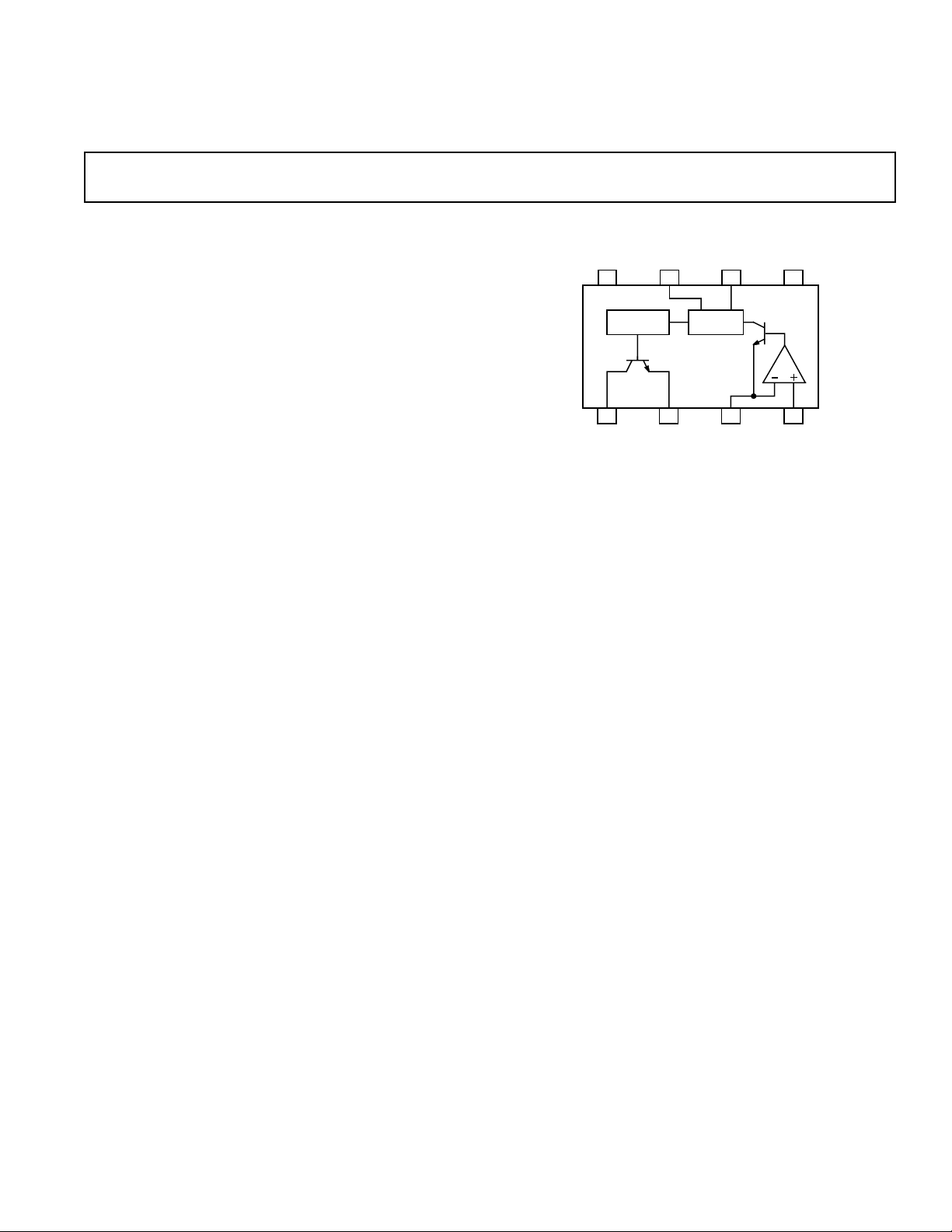
FUNCTIONAL BLOCK DIAGRAM
2. A minimum number of low cost external components are
necessary. A single RC network is all that is required to set
up any full scale frequency up to 500 kHz and any full-scale
input voltage up to ±30 V.
3. Plastic packaging allows low cost implementation of the
standard VFC applications: A/D conversion, isolated signal
transmission, F/V conversion, phase-locked loops, and tuning
switched-capacitor filters.
4. Power supply requirements are minimal; only 2.0 mA of
quiescent current is drawn from the single positive supply
from 4.5 volts to 36 volts. In this mode, positive inputs can
vary from 0 volts (ground) to (+V
can easily be connected for below ground operation.
5. The versatile open-collector output stage can sink more than
10 mA with a saturation voltage less than 0.4 volts. The Logic
Common terminal can be connected to any level between
ground (or –V
) and 4 volts below +VS. This allows easy
S
direct interface to any logic family with either positive or
negative logic levels.
–4) volts. Negative inputs
S
REV. B
Information furnished by Analog Devices is believed to be accurate and
reliable. However, no responsibility is assumed by Analog Devices for its
use, nor for any infringements of patents or other rights of third parties
which may result from its use. No license is granted by implication or
otherwise under any patent or patent rights of Analog Devices.
One Technology Way, P.O. Box 9106, Norwood, MA 02062-9106, U.S.A.
Tel: 781/329-4700 World Wide Web Site: http://www.analog.com
Fax: 781/326-8703 © Analog Devices, Inc., 1999

(TA = +25ⴗC and VS (total) = 5 V to 16.5 V, unless otherwise noted. All testing done
AD654–SPECIFICATIONS
@ VS = +5 V.)
AD654JN/JR
Model Min Typ Max Units
CURRENT-TO-FREQUENCY CONVERTER
Frequency Range 0 500 kHz
Nonlinearity
f
MAX
f
MAX
1
= 250 kHz 0.06 0.1 %
= 500 kHz 0.20 0.4 %
Full-Scale Calibration Error
C = 390 pF, I
vs. Supply (f
= +4.75 V to +5.25 V 0.20 0.40 %/V
V
S
= +5.25 V to +16.5 V 0.05 0.10 %/V
V
S
= 1.000 mA –10 +10 %
IN
≤ 250 kHz)
MAX
vs. Temp (0°C to +70°C) 50 ppm/°C
ANALOG INPUT AMPLIFIER
(Voltage-to-Current Converter)
Voltage Input Range
Single Supply 0 (+V
Dual Supply –V
S
– 4) V
S
(+VS – 4) V
Input Bias Current
(Either Input) 30 50 nA
Input Offset Current 5 nA
Input Resistance (Noninverting) 250 MΩ
Input Offset Voltage 0.5 1.0 mV
vs. Supply
= +4.75 V to +5.25 V 0.1 0.25 mV/V
V
S
= +5.25 V to +16.5 V 0.03 0.1 mV/V
V
S
vs. Temp (0°C to +70°C) 4 µV/°C
OUTPUT INTERFACE (Open Collector Output)
(Symmetrical Square Wave)
Output Sink Current in Logic “0”
V
= 0.4 V max, +25°C 10 20 mA
OUT
= 0.4 V max, 0°C to +70°C510 mA
V
OUT
2
Output Leakage Current in Logic “1” 10 100 nA
0°C to +70°C 50 500 nA
Logic Common Level Range –V
Rise/Fall Times (C
= 1 mA 0.2 µs
I
IN
I
= 1 µA1µs
IN
= 0.01 µF)
T
S
(+VS – 4) V
POWER SUPPLY
Voltage, Rated Performance 4.5 16.5 V
Voltage, Operating Range
Single Supply 4.5 36 V
Dual Supply ±5 ±18 V
Quiescent Current
(Total) = 5 V 1.5 2.5 mA
V
S
VS (Total) = 30 V 2.0 3.0 mA
TEMPERATURE RANGE
Operating Range –40 +85 °C
NOTES
1
At f
= 250 kHz; R
MAX
1
At f
= 500 kHz; R
MAX
2
The sink current is the amount of current that can flow into Pin 1 of the AD654 while maintaining a maximum voltage of 0.4 V between Pin 1 and Logic Common.
Specifications shown in boldface are tested on all production units at final electrical test. Results from those tests are used to calculate outgoing quality levels. All min
and max specifications are guaranteed, although only those shown in boldface are tested on all production units.
Specifications subject to change without notice.
= 1 kΩ, C
T
= 1 kΩ, C
T
= 390 pF, IIN = 0 mA–1 mA.
T
= 200 pF, IIN = 0 mA–1 mA.
T
–2–
REV. B

AD654
ABSOLUTE MAXIMUM RATING
Total Supply Voltage +VS to –VS . . . . . . . . . . . . . . . . . . . 36 V
Maximum Input Voltage
(Pins 3, 4) to –V
Maximum Output Current
Instantaneous . . . . . . . . . . . . . . . . . . . . . . . . . . . . . . . 50 mA
Sustained . . . . . . . . . . . . . . . . . . . . . . . . . . . . . . . . . . 25 mA
Logic Common to –V
Storage Temperature Range . . . . . . . . . . . . . –65°C to +150°C
Model Temperature Range Package Description Package Option
AD654JN –40°C to +85°C 8-Lead Plastic DIP N-8
AD654JR –40°C to +85°C 8-Lead SOIC SO-8
. . . . . . . . . . . . . . . . . . . . –300 mV to +V
S
. . . . . . . . . . . . . . . –500 mV to (+VS –4)
S
ORDERING GUIDE
S
REV. B
–3–
AD654
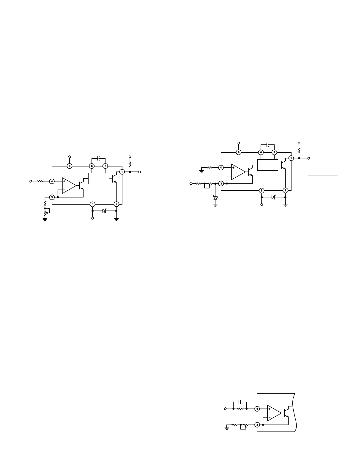
(
)
OSC/
DRIVER
AD654
OPTIONAL
R
COMP
CR1
–V
S
(0V TO –15V)
R1 R2
+V
S
(+5V TO –VS +30)
C
T
+V
LOGIC
R
PU
F
OUT
F
OUT
=
V
IN
(10V) (R1 + R2) C
T
V
IN
CLAMP
DIODE
CIRCUIT OPERATION
The AD654’s block diagram appears in Figure 1. A versatile
operational amplifier serves as the input stage; its purpose is to
convert and scale the input voltage signal to a drive current in the
NPN follower. Optimum performance is achieved when, at the
full-scale input voltage, a 1 mA drive current is delivered to the
current-to-frequency converter (an astable multivibrator). The
drive current provides both the bias levels and the charging current
to the externally connected timing capacitor. This “adaptive” bias
scheme allows the oscillator to provide low nonlinearity over
the entire current input range of 100 nA to 2 mA. The square
wave oscillator output goes to the output driver which provides
a floating base drive to the NPN power transistor. This floating
V/F CONNECTIONS FOR NEGATIVE INPUT VOLTAGE
OR CURRENT
The AD654 can accommodate a wide range of negative input
voltages with proper selection of the scaling resistor, as indicated
in Figure 2. This connection, unlike the buffered positive connection, is not high impedance because the signal source must
supply the 1 mA FS drive current. However, large negative voltages beyond the supply can be handled easily by modifying the
scaling resistors appropriately. If the input is a true current source,
R1 and R2 are not used. Again, diode CR1 prevents latch-up by
insuring Logic Common does not drop more than 500 mV below
. The clamp diode (MBD101) protects the AD654 input
–V
S
from “below –V
” inputs.
S
drive allows the logic interface to be referenced to a level other
OPTIONAL
IN
R
S
COMP
R1
R2
.
+V
S
(+5V TO –VS +30)
C
OSC/
DRIVER
AD654
–V
S
0V TO –15V
T
CR1
+V
LOGIC
F
OUT
R
PU
F
OUT
V
=
IN
(10V) (R1 + R2) C
T
Figure 2. V-F Connections for Negative Input Voltages or
Current
than –V
V
Figure 1. Standard V-F Connection for Positive Input
Voltages
OFFSET CALIBRATION
In theory, two adjustments calibrate a V/F: scale and offset. In
V/F CONNECTION FOR POSITIVE INPUT VOLTAGES
In the connection scheme of Figure 1, the input amplifier presents
a very high (250 MΩ) impedance to the input voltage, which
is converted into the proper drive current by the scaling resistors
at Pin 3. Resistors R1 and R2 are selected to provide a 1 mA
full-scale current with enough trim range to accommodate the
AD654’s 10% FS error and the components’ tolerances. Fullscale currents other than 1 mA can be chosen, but linearity will
be reduced; 2 mA is the maximum allowable drive. The AD654’s
positive input voltage range spans from –V
(ground in sink supply
S
operation) to four volts below the positive supply. Power supply rejection degrades as the input exceeds (+V
– 3.5 V) the output frequency goes to zero.
(+V
S
– 3.75 V) and at
S
As indicated by the scaling relationship in Figure 1, a 0.01 µF
timing capacitor will give a 10 kHz full-scale frequency, and
0.001 µF will give 100 kHz with a 1 mA drive current. Good V/F
linearity requires the use of a capacitor with low dielectric
absorption (DA), while the most stable operation over temperature calls for a component having a small tempco. Polystyrene,
polypropylene, or Teflon* capacitors are preferred for tempco and
dielectric absorption; other types will degrade linearity. The
capacitor should be wired very close to the AD654. In Figure 1,
Schottky diode CR1 (MBD101) prevents logic common from
dropping more than 500 mV below –V
required if –V
*Teflon is a trademark of E.I. Du Pont de Nemours & Co.
S
. This diode is not
S
is equal to logic common.
practice, most applications find the AD654’s 1 mV max voltage
offset sufficiently low to forgo offset calibration. However, the
input amplifier’s 30 nA (typ) bias currents will generate an offset
due to the difference in dc sound resistance between the input
terminals. This offset can be substantial for large values of R
R1 + R2 and will vary as the bias currents drift over temperature.
Therefore, to maintain the AD654’s low offset, the application may
require balancing the dc source resistances at the inputs (Pins
3 and 4).
For positive inputs, this is accomplished by adding a compensation
resistor nominally equal to R
in series with the input as shown
T
in Figure 3a. This limits the offset to the product of the 30 nA
bias current and the mismatch between the source resistance R
and R
offset current flowing through the source resistance R
. A second, smaller offset arises from the inputs’ 5 nA
COMP
or R
T
COMP
For negative input voltage and current connections, the compensation resistor is added at Pin 4 as shown in Figure 3b in lieu of
grounding the pin directly. For both positive and negative inputs,
the use of R
may lead to noise coupling at Pin 4 and should
COMP
therefore be bypassed for lowest noise operation.
(OPTIONAL)
C
V
IN
R
COMP
R1 R2
AD654
Figure 3a. Bias Current Compensation—Positive Inputs
–4–
REV. B
=
T
T
.

AD654
AD654
R
OFF
100kV
R4
392V
R3
1kV
60.6V
*
*OPTIONAL
OFFSET TRIM
f =
I
S
(20V) C
T
I
R
–V
1mA
FS
I
S
R2
100V
R1
100V
(OPTIONAL)
C
R
COMP
R1 R2
V
IN
AD654
Figure 3b. Bias Current Compensation—Negative Inputs
If the AD654’s 1 mV offset voltage must be trimmed, the trim
must be performed external to the device. Figure 3c shows an
optional connection for positive inputs in which R
add a variable resistance in series with RT. A variable
R
OFF2
source of ±0.6 V applied to R
then adjusts the offset ±1 mV.
OFF1
Similarly, a ±0.6 V variable source is applied to R
OFF1
OFF
and
in Fig-
ure 3d to trim offset for negative inputs. The ±0.6 V bipolar
source could simply be an AD589 reference connected as shown
in Figure 3e.
AD654
R
OFF2
20V
R
OFF1
10kV
V
IN
5kV 8.25kV
60.6V
10kV
linearity, it is unnecessary for the end-user to perform this tedious
and time consuming test on a routine basis.
Sufficient FS calibration trim range must be provided to accommodate the worst-case sum of all major scaling errors. This
includes the AD654’s 10% full-scale error, the tolerance of the
fixed scaling resistor, and the tolerance of the timing capacitor.
Therefore, with a resistor tolerance of 1% and a capacitor tolerance
of 5%, the fixed part of the scaling resistor should be a maximum
of 84% of nominal, with the variable portion selected to allow
116% of the nominal.
If the input is in the form of a negative current source, the scaling
resistor is no longer required, eliminating the capability of trimming FS frequency in this fashion. Since it is usually not practical
to smoothly vary the capacitance for trimming purposes, an
alternative scheme such as the one shown in Figure 4 is needed.
Designed for a FS of 1 mA, this circuit divides the input into two
Figure 3c. Offset Trim Positive Input (10 V FS)
R
5.6MV
10kV
60.6V
OFF
AD654
and flowing into Pin 3; it constitutes the signal current IT to be
converted. The second path, through another 100 Ω resistor R2,
carries the same nominal current. Two equal valued resistors
Figure 4. Current Source FS Trim
offer the best overall stability, and should be either 1% discrete
V
IN
5kV8.25kV
film units, or a pair from a common array.
Since the 1 mA FS input current is divided into two 500 µA legs
(one to ground and one to Pin 3), the total input signal current
Figure 3d. Offset Trim Negative Input (–10 V FS)
R1
10kVR110kV
+5V
R3
+
–5V
AD589
R2
10kV
10kV
–
R4
10kV
100kV
R5
60.6V
(I
) is divided by a factor of two in this network. To achieve the
S
same conversion scale factor, C
must be reduced by a factor of
T
two. This results in a transfer unique to this hookup:
I
f =
S
(20V ) C
T
For calibration purposes, resistors R3 and R4 are added to the
network, allowing a ±15% trim of scale factor with the values
shown. By varying R4’s value the trim range can be modified to
accommodate wider tolerance components or perhaps the cali-
Figure 3e. Offset Trim Bias Network
FULL-SCALE CALIBRATION
Full-scale trim is the calibration of the circuit to produce the
desired output frequency with a full-scale input applied. In most
cases this is accomplished by adjusting the scaling resistor R
Precise calibration of the AD654 requires the use of an accurate
voltage standard set to the desired FS value and an accurate
frequency meter. A scope is handy for monitoring output waveshape. Verification of converter linearity requires the use of a
switchable voltage source or DAC having a linearity error below
±0.005%, and the use of long measurement intervals to mini-
mize count uncertainties. Since each AD654 is factory tested for
REV. B
.
T
bration tolerance on a current output transducer such as the
AD592 temperature sensor. Although the values of R1–R4 shown
are valid for 1 mA FS signals only, they can be scaled upward
proportionately for lower FS currents. For instance, they should
be increased by a factor of ten for a FS current of 100 µA.
In addition to the offsets generated by the input amplifier’s bias
and offset currents, an offset voltage induced parasitic current
arises from the current fork input network. These effects are
minimized by using the bias current compensation resistor R
and offset trim scheme shown in Figure 3e.
Although device warm-up drifts are small, it is good practice to
allow the devices operating environment to stabilize before trim,
–5–
OFF

AD654
817
26354
AD654
+5V
GND
DIGITAL
P.S.
10V
0.1mF
C
T
R
T
R
PU
f
OUT
AGND
V
IN
and insure the supply, source and load are appropriate. If provision
is made to trim offset, begin by setting the input to 1/10,000 of
full scale. Adjust the offset pot until the output is 1/10,000 of
full scale (for example, 25 Hz for a FS of 250 kHz). This is most
easily accomplished using a frequency meter connected to the
output. The FS input should then be applied and the gain pot
should be adjusted until the desired FS frequency is indicated.
INPUT PROTECTION
The AD654 was designed to be used with a minimum of additional
hardware. However, the successful application of a precision IC
involves a good understanding of possible pitfalls and the use of
suitable precautions. Thus +V
more than 300 mV below –V
not drop more than 500 mV below –V
and RT pins should not be driven
IN
. Likewise, Logic Common should
S
. This would cause inter-
S
nal junctions to conduct, possibly damaging the IC. In addition
to the diode shown in Figures 1 and 2 protecting Logic Common,
a second Schottky diode (MBD101) can protect the AD654’s
inputs from “below –V
desirable not to drive +V
converter will exhibit a zero output for inputs above (+V
’’ inputs as shown in Figure 5. It is also
S
and RT above +VS. In operation, the
IN
– 3.5 V).
S
Also, control currents above 2 mA will increase nonlinearity.
The AD654’s 80 dB dynamic range guarantees operation from a
control current of 1 mA (nominal FS) down to 100 nA (equivalent to 1 mV to 10 V FS). Below 100 nA improper operation of
the oscillator may result, causing a false indication of input
amplitude. In many cases this might be due to short-lived noise
spikes which become added to input. For example, when scaled
to accept an FS input of 1 V, the –80 dB level is only 100 µV, so
when the mean input is only 60 dB below FS (1 mV), noise spikes
of 0.9 mV are sufficient to cause momentary malfunction.
This effect can be minimized by using a simple low-pass filter
ahead of the converter or a guard ring around the R
pin. The
T
filter can be assembled using the bias current compensation
resistor discussed in the previous section. For an FS of 10 kHz,
a single-pole filter with a time constant of 100 ms will be suitable,
but the optimum configuration will depend on the application
and the type of signal processing. Noise spikes are only likely to
be a cause of error when the input current remains near its minimum value for long periods of time; above 100 nA full integration
of additive input noise occurs. Like the inputs, the capacitor
terminals are sensitive to interference from other signals. The
timing capacitor should be located as close as possible to the
AD654 to minimize signal pickup in the leads. In some cases,
guard rings or shielding may be required.
AD654
I
IN
MBD101
DECOUPLING
It is good engineering practice to use bypass capacitors on the
supply-voltage pins and to insert small-valued resistors (10 to
100 Ω) in the supply lines to provide a measure of decoupling
Figure 5. Input Protection
between the various circuits in the system. Ceramic capacitors
of 0.1 µF to 1.0 µF should be applied between the supply-
voltage pins and analog signal ground for proper bypassing on
the AD654. A proper ground scheme appears in Figure 6.
Figure 6. Proper Ground Scheme
OUTPUT INTERFACING CONSIDERATION
The output stage’s design allows easy interfacing to all digital logic
families. The output NPN transistor’s emitter and collector are
both uncommitted. The emitter can be tied to any voltage between
and 4 volts below +VS, and the open collector can be pulled
–V
S
up to a voltage 36 volts above the emitter regardless of +V
S
high power output stage can sink over 10 mA at a maximum
saturation voltage of 0.4 V. The stage limits the output current
at 25 mA and can handle this limit indefinitely without damaging the device.
NONLINEARITY SPECIFICATION
The preferred method of specifying nonlinearity error is in terms
of maximum deviation from the ideal relationship after calibrating the converter at full scale. This error will vary with the full
scale frequency and the mode of operation. The AD654 operates
best at a 150 kHz full-scale frequency with a negative voltage input;
the linearity is typically within 0.05%. Operating at higher frequencies or with positive inputs will degrade the linearity as
indicated in the Specifications Table. Typical linearity at various
temperatures is shown in Figure 7.
10
5
1
0.5
0.10
0.05
MAXIMUM NONLINEARITY – %
0.01
10
150 250 350 500
FULL-SCALE FREQUENCY – kHz
f
= 08C TO +858C
AMB
f
AMB
= –408C
Figure 7. Typical Nonlinearities at Different Full-Scale
Frequencies
–6–
REV. B
. The

AD654
5V
(ISOLATED)
R1
390V
4N37
OPTO-ISOLATOR
5V
(LOCAL)
GRN
LED
OSC/
DRIVER
R
T
1kV
V
IN
(0V TO 1V)
C
T
1000pF
AD654
R3
270V
74LS14
Q1
2N3904
R2
120V
V/F OUTPUT
FS = 100kHz
TTL
ISOLATED LOCAL
f
=
1mF
AD654
DRIVER
0.01mF
I
T
(10V) C
1N4148
OSC/
C
T
T
AD589
+
–
AD592
1mA/kV
R1
R4
R2
R3
R5
Figure 8. Two-Wire Temperature-to-Frequency Converter
TWO-WIRE TEMPERATURE-TO-FREQUENCY
CONVERSION
Figure 8 shows the AD654 in a two-wire temperature-to-frequency
conversion scheme. The twisted pair transmission line serves the
dual purpose of supplying power to the device and also carrying
frequency data in the form of current modulation.
The positive supply line is fed to the remote V/F through a
140 Ω resistor. This resistor is selected such that the quiescent
current of the AD654 will cause less than one V
to be dropped.
BE
As the V/F oscillates, additional switched current is drawn through
R
when Pin 1 goes low. The peak level of this additional cur-
L
rent causes Q1 to saturate, and thus regenerates the AD654’s
output square wave at the collector. The supply voltage to the
AD654 then consists of a dc level, less the resistive line drop, plus a
one V
p-p square wave at the output frequency of the AD654.
BE
This ripple is reduced by the diode/capacitor combination.
To set up the receiver circuit for a given voltage, the R
and R
S
L
resistances are selected as shown in Table I. CMOS logic stages
can be driven directly from the collector of Q1, and a single TTL
load can be driven from the junction of R
and R6.
S
Table I.
+V
S
RS (⍀)R
(⍀)
L
10 V 270 1.8k
15 V 680 2.7k
R
T
V
S
(10V TO 15V)
140V
Q1
2N3906
R
S
R6
220V
CMOS
OUTPUT
TTL
OUTPUT
(1 LOAD)
values shown in Table II. Since temperature is the parameter of
interest, an NPO ceramic capacitor is used as the timing capacitor for low V/F TC.
When scaling per K, resistors R1–R3 and the AD589 voltage
reference are not used. The AD592 produces a 1 µA/K current
output which drives Pin 3 of the AD654. With the timing
capacitor of 0.01 µF this produces an output frequency scaled to
10 Hz/K. When scaling per °C and °F, the AD589 and resistors
R1–R3 offset the drive current at Pin 3 by 273.2 µA for scaling
per °C and 255.42 µA for scaling per °F. This will result in fre-
quencies sealed at 10 Hz/°C and 5.55 Hz/°F, respectively.
OPTOISOLATOR COUPLING
A popular method of isolated signal coupling is via optoelectronic isolators, or optocouplers. In this type of device, the signal is
coupled from an input LED to an output photo-transistor, with
light as the connecting medium. This technique allows dc to be
transmitted, is extremely useful in overcoming ground loop
problems between equipment, and is applicable over a wide
range of speeds and power.
Figure 9 shows a general purpose isolated V/F circuit using a
low cost 4N37 optoisolator. A +5 V power supply is assumed for
both the isolated (+5 V isolated) and local (+5 V local) supplies.
The input LED of the isolator is driven from the collector output of the AD654, with a 9 mA current level established by R1
for high speed, as well as for a 100% current transfer ratio.
Table II.
(+VS) R1 (⍀) R2 (⍀) R3 (⍀) R4 (⍀) R5 (⍀)
10 V – – – 100k 127k
K
15 V – – – 100k 127k
10 V 6.49k 4.02k 1k 95.3k 22.6k
°C
15 V 12.7k 4.02k 1k 78.7k 36.5k
10 V 6.49k 4.42k 1k 154k 22.6k
°F
15 V 12.7k 4.42k 1k 105k 36.5k
At the V/F end, the AD592C temperature transducer is interfaced with the AD654 in such a manner that the AD654 output
F = 10 Hz/K
F = 10 Hz/°C
F = 5.55 Hz/°F
frequency is proportional to temperature. The output frequency
can be sealed and offset from K to °C or °F using the resistor
REV. B
Figure 9. Optoisolator Interface
–7–

AD654
C
At the receiver side, the output transistor is operated in the
photo-transistor mode; that is with the base lead (Pin 6) open.
This allows the highest possible output current. For reasonable
speed in this mode, it is imperative that the load impedance be
as low as possible. This is provided by the single transistor stage
current-to-voltage converter, which has a dynamic load impedance of less than 10 ohms and interfaces with TTL at the output.
USING A STAND-ALONE FREQUENCY COUNTER/LED
DISPLAY DRIVER FOR VOLTMETER APPLICATIONS
Figure 10 shows the AD654 used with a stand-alone frequency
counter/LED display driver. With C
= 1000 pF and R
T
the AD654 produces an FS frequency of 100 kHz when V
= 1 kΩ
T
IN
=
+1 V. This signal is fed into the ICM7226A, a universal counter
system that drives common anode LEDs. With the FUNCTION
pin tied to D1 through a 10 kΩ resistor the ICM7226A counts the
frequency of the signal at A
. This count period is selected by
IN
the user and can be 10 ms, 100 ms, 1s, or 10 seconds, as shown on
Pin 21. The longer the period selected, the more resolution the
count will have. The ICM7226A then displays the frequency on
the LEDs, driving them directly as shown. Refreshing of the LEDs
is handled automatically by the ICM7226. The entire circuit operates on a single +5 V supply and gives a meter with 3, 4, or 5
digit resolution.
5V 5V
1kV
AD654
FUNCTION
dp
e
g
a
GND
d
b
c
f
8
7
6
5
OSL OUT
ICM7226A
AIN
HOLD
OSL JN
RANGE
1000pF
NC
NC
D1
D2
D3
D4
D5
V+
D6
D7
D8
40
30kV
39
38
37
5V
36
35
34
5V
33
32
31
30
29
28
27
26
25
24
23
22
21
5V
10kV
10MHz
CRYSTAL
22MV
39pF 39pF
5V 5V
D1 (10ms)
D2 (100ms)
D3 (1s)
D4 (10s)
4
8
+
V
IN
(0V TO 1V)
–
DI PIN 30
500V
1kV
825V
10kV
1
2
3
4
1
2
3
4
5
6
7
8
9
10
11
12
13
14
15
16
17
18
19
20
8
Longer count periods not only result in the count having more
resolution, they also serve as an integration of noisy analog signals.
For example, a normal-mode 60 Hz sine wave riding on the input
of the AD654 will result in the output frequency increasing on
the positive half of the sine wave and decreasing on the negative
half of the sine wave. This effect is cancelled by selecting a count
period equal to an integral number of noise signal periods. A
100 ms count period is effective because it not only has an integral number of 60 Hz cycles (6), it also has an integral number
of 50 Hz cycles (5). This is also true of the 1 second and 10 second count period.
AD654-BASED ANALOG-TO-DIGITAL CONVERSION
USING A SINGLE CHIP MICROCOMPUTER
The AD654 can serve as an analog-to-digital converter when
used with a single component microcomputer that has an interval timer/event counter such as the 8048. Figure 11 shows the
AD654, with a full-scale input voltage of +1 V and a full-scale
output frequency of 100 kHz, connected to the timer/counter
input Pin T1 of the 8048. Such a system can also operate on a
single +5 V supply.
The 8748 counter is negative edge triggered; after the STRT
CNT instruction is executed subsequent high to low transitions
on T1 increment the counter. The maximum rate at which the
counter may be incremented is once per three instruction cycles;
using a 6 MHz crystal, this corresponds to once every 7.5 µs, or
a maximum frequency of 133 kHz. Because the counter overflows
every 256 counts (8 bits), the timer interrupt is enabled. Each
overflow then causes a jump to a subroutine where a register is
incremented. After the STOP TCNT instruction is executed, the
number of overflows that have occurred will be the number in
this register. The number in this register multiplied by 256 plus
the number in the counter will be the total number of negative
edges counted during the count period. The count period is
handled simply by decrementing a register the number of times
necessary to correspond to the desired count time. After the
register has been decremented the required number of times the
STOP TCNT instruction is executed.
The total number of negative edges counted during the count
period is proportional to the input voltage. For example, if a 1 V
full-scale input voltage produces a 100 kHz signal and the count
period is 100 ms, then the total count will be 10,000. Scaling
from this maximum is then used to determine the input voltage,
i.e., a count of 5000 corresponds to an input voltage of 0.5 V.
As with the ICM7226, longer count times result in counts having more resolution; and they result in the integration of noisy
analog signals.
D.P. g e d c b af
LED
OVERFLOW
INDICATOR
D8 D7 D6 D5 D4 D3 D2 D1
N
= NO CONNECT
Figure 10. AD654 With Stand-Alone Frequency Counter/
LED Display Driver
–8–
REV. B

AD654
+
V
IN
(0V TO 1V)
–
1kV
5V GND
FREQUENCY DOUBLING
Since the AD654’s output is a square-wave rather than a pulse
train, information about the input signal is carried on both
20pF
6MHz
20pF
1mF
NC
10kV
1
2
AD654
3
4
825V
1%
500V
D
A
XTAL1
XTAL2
RESET
EA
SS
INT
T0
T1
ALE
5V
8
7
6
5
VCCVDDV
8048
PROG
PSEN
NC NC
1000pF
SS
P10
P17
P20
P27
DB0
DB7
WR RD
NC = NO CONNECT
PORT 1
PORT 2
BUS
PORT
halves of the output waveform. The circuit in Figure 12 converts
the output into a pulse train, effectively doubling the output
frequency, while preserving the better low frequency linearity of
the AD654. This circuit also accommodates an input voltage
that is greater than the AD654 supply voltage.
Resistors R1–R3 are used to scale the 0 V to +10 V input voltage
down to 0 V to +1 V as seen at Pin 4 of the AD654. Recall that
V
must be less than V
IN
–4 V, or in this case less than 1 V.
SUPPLY
The timing resistor and capacitor are selected such that this 0 V
to +1 V signal seen at Pin 4 results in a 0 kHz to 200 kHz output
frequency.
The use of R4, C1 and the XOR gate doubles this 200 kHz
output frequency to 400 kHz. The AD654 output transistor is
basically used as a switch, switching capacitor C1 between a
charging mode and a discharging mode of operation. The voltages
seen at the input of the 74LS86 are shown in the waveform diagram. Due to the difference in the charge and discharge time
constants, the output pulse widths of the 74LS86 are not equal.
The output pulse is wider when the capacitor is charging due to
its longer rise time than fall time. The pulses should therefore be
counted on their rising, rather than falling, edges.
Figure 11. AD654 VFC as an ADC
R2
R1
2kV
8.06kV
V
IN
(0V TO 10V)
1kV
R3
R
T
1kV
5V
R
AD654
TRANSISTOR
OSC/
DRIVER
C
T
500pF
OFF
ON
A
B
C
V
0
V
0
5
0
WAVEFORM DIAGRAM
2.87kV
1000pF
Figure 12. Frequency Doubler
PU
C1
R4
1kV
A
B
74LS86
C
V/F OUTPUT
FS = 400MHz
REV. B
–9–

AD654
+15V
10mF
+
V
IN
(0V TO 1V)
–
1kV
0.1mF
R
= 1kV
T
+5V
0.1mF
1
2
AD654
3
4
A
8
7
6
5
V1
C
T
100pF
MINIMUM
DISTANCE
Q1
Q2
68kV
J270
J270
+15V
68kV
Figure 13. 2 MHz, Frequency Doubling V/F
OPERATION AT HIGHER OUTPUT FREQUENCIES
Operation of the AD654 via the conventional output (Pins 1 and
2) is speed limited to approximately 500 kHz for reasons of TTL
logic compatibility. Although the output stage may become
speed limited, the multivibrator core itself is able to oscillate to
1 MHz or more. The designer may take advantage of this feature in
order to operate the device at frequencies in excess of 500 kHz.
Figure 13 illustrates this with a circuit offering 2 MHz full scale.
In this circuit the AD654 is operated at a full scale (FS) of 1 mA,
with a C
of 1 MHz across C
of 100 pF. This achieves a basic device FS frequency
T
. The P channel JFETs, Q1 and Q2, buffer
T
the differential timing capacitor waveforms to a low impedance
level where the push-pull signal is then ac coupled to the high speed
comparator A2. Hysteresis is used, via R7, for nonambiguous
switching and to eliminate the oscillations which would otherwise occur at low frequencies.
The net result of this is a very high speed circuit which does not
compromise the AD654 dynamic range. This is a result of the FET
buffers typically having only a few pA of bias current. The high
end dynamic range is limited, however, by parasitic package and
layout capacitances in shunt with CT, as well as those from each node
to ac ground. Minimizing the lead length between A2–6/A2–7 and
Q1/Q2 in PC layout will help. A ground plane will also help
stability. Figure 14 shows the waveforms V1–V4 found at the
respective points shown in Figure 13.
18V
470pF
A3 = 74LS86
A3-d
A3-c
A3-b
V4
V2
MINIMUM
DISTANCE
10mF
+
10mF
5.9kV
1%
(32)
D
8.2V
0.1mF
10mF
0.1mF
D
R7
V3
A2
LM360
A3-a
–5V
The output of the comparator is a complementary square wave
at 1 MHz FS. Unlike pulse train output V/F converters, each
half-cycle of the AD654 output conveys information about the
input. Thus it is possible to count edges, rather than full cycles
of the output, and double the effective output frequency. The
XOR gate following A2 acts as an edge detector producing a short
pulse for each input state transition. This effectively doubles the
V/F FS frequency to 2 MHz. The final result is a 1 V full-scale
input V/F with a 2 MHz full-scale output capability; typical
nonlinearity is 0.5%.
500ns
100
90
10
0%
2V 5V
2V 5V
2V
V1
0
2V
V2
0
5V
V3
0
5V
V4
0
Figure 14. Waveforms of 2 MHz Frequency Doubler
–10–
REV. B
PIN 1
0.210 (5.33)
MAX
0.160 (4.06)
0.115 (2.93)
0.022 (0.558)
0.014 (0.356)
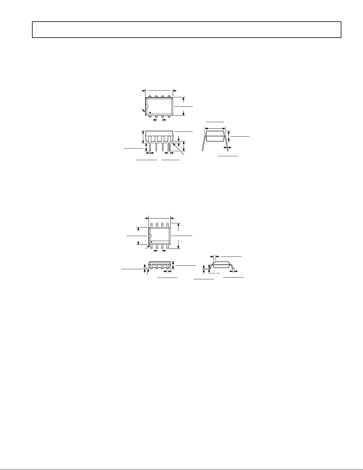
OUTLINE DIMENSIONS
Dimensions shown in inches and (mm).
8-Lead Plastic DIP (N-8)
0.430 (10.92)
0.348 (8.84)
8
0.100 (2.54)
1
BSC
5
0.280 (7.11)
0.240 (6.10)
4
0.060 (1.52)
0.015 (0.38)
0.070 (1.77)
0.045 (1.15)
0.130
(3.30)
MIN
SEATING
PLANE
0.325 (8.25)
0.300 (7.62)
0.015 (0.381)
0.008 (0.204)
8-Lead SOIC (SO-8)
(Narrow Body)
0.195 (4.95)
0.115 (2.93)
AD654
C900d–0–12/99 (rev. B)
0.1574 (4.00)
0.1497 (3.80)
PIN 1
0.0098 (0.25)
0.0040 (0.10)
SEATING
0.1 968 (5.00)
0.1 890 (4.80)
85
0.0500 (1.27)
BSC
0.0192 (0.49)
0.0138 (0.35)
PLANE
0.2440 (6.20)
0.2284 (5.80)
41
0.0688 (1.75)
0.0532 (1.35)
0.0098 (0.25)
0.0075 (0.19)
0.0196 (0.50)
0.0099 (0.25)
88
0.0500 (1.27)
08
0.0160 (0.41)
x 458
PRINTED IN U.S.A.
REV. B
–11–
 Loading...