Analog Devices AD5602 12 22 pB Datasheet

2.7 V to 5.5 V, <100 µA,
8/10/12 Bit D/A with I2C Compatible
Interface, tiny SC70 Package
Preliminary Technical Data
FEATURES
Single 8/10/12-bit DAC, 2 LSB INL
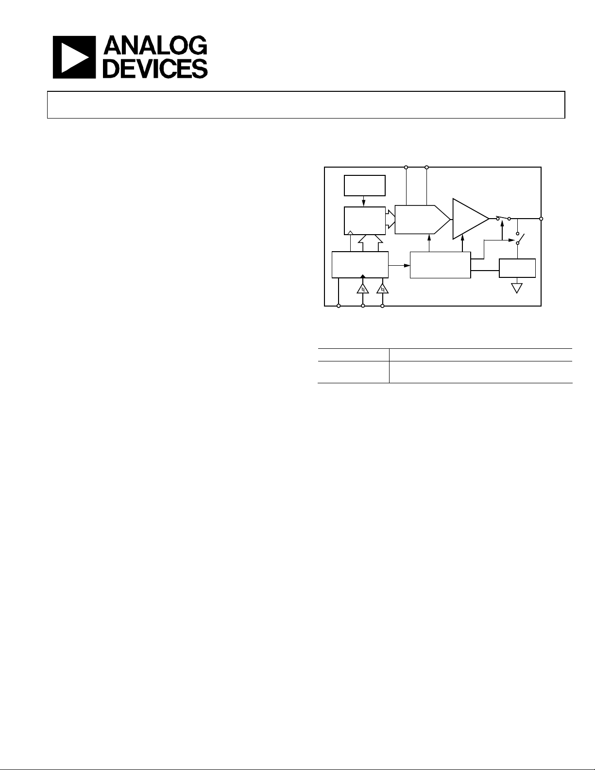
FUNCTIONAL BLOCK DIAGRAM
V
DD
GND
AD5602/12/22
6-lead SC70 package
Micropower operation: max 100 µA @ 5 V
Power-down to <100 nA @ 3 V
POWER-ON
RESET
2.7 V to 5.5 V power supply
Guaranteed monotonic by design
Power-on-reset to 0 V with brownout detection
3 power-down functions
2CR
Compatible Serial Interface supports:
I
Standard (100KHz), Fast (400KHz) and
High-Speed (3.4MHz) Modes
On-chip output buffer amplifier, rail-to-rail operation
DAC
REGISTER
INPUT
CONTROL
LOGIC
REF(+)
8/10/12-BIT
DAC
POWER-DOWN
CONTROL LOGIC
OUTPUT
BUFFER
APPLICATIONS
Process control
Data acquisition systems
Portable battery-powered instruments
Digital gain and offset adjustment
Programmable voltage and current sources
Programmable attenuators
ADDR
SCL SDA
Figure 1
RELATED DEVICES
Part No. Description
AD5601/11/21
2.7V to 5.5 V, <100µA, 8/10/12 Bit nanoDACTM
D/A with SPI Interface in a tiny SC70 package
AD5602/12/22
RESISTOR
NETWORK
V
OUT
GENERAL DESCRIPTION
The AD5602/12/22, a member of the nanoDACTM D/A family is
a single, 8/10/12-bit buffered voltage out DAC that operates
from a single +2.7 V to +5.5 V supply consuming <100 µA at
5 V, and comes in a tiny SC70 package. Its on-chip precision
output amplifier allows rail-to-rail output swing to be achieved.
2
The AD5602/12/22 utilizes a 2-wire I
C compatible serial
interface that operates in Standard (100 KHz), Fast (400 KHz)
and High-Speed (3.4 MHz) Modes.
The reference for AD5602/12/22 is derived from the power
supply inputs and thus gives the widest dynamic output range.
The part incorporates a power-on-reset circuit that ensures the
DAC output powers up to 0 V and remains there until a valid
write takes place to the device. The part contains a power-down
feature that reduces the current consumption of the device to
<100 nA at 3 V and provides software selectable output loads
while in power-down mode. The part is put into power-down
mode over the serial interface. The low power consumption of
this part in normal operation makes it ideally suited to portable
battery operated equipment. The power consumption is
0.5 mW at 5 V.
Rev. PrB 18-Feb-05
Information furnished by Analog Devices is believed to be accurate and reliable.
However, no responsibility is assumed by Analog Devices for its use, nor for any
infringements of patents or other rights of third parties that may result from its use.
Specifications subject to change without notice. No license is granted by implication
or otherwise under any patent or patent rights of Analog Devices. Trademarks and
registered trademarks are the property of their respective owners.
PRODUCT HIGHLIGHTS
1. Available in 6-lead SC70.
2. Max 100µA power consumption, single-supply operation.
This part operates from a single 2.7 V to 5.5 V supply and
typically consumes 0.2 mW at 3 V and 0.5 mW at 5 V,
making it ideal for battery-powered applications.
3. The on-chip output buffer amplifier allows the output of
the DAC to swing rail-to-rail with a typical slew rate of
0.5 V/µs.
4. Reference derived from the power supply.
2
5. Standard, Fast and High-Speed Mode I
C interface.
6. Designed for very low power consumption.
7. Power-down capability. When powered down, the DAC
typically consumes <100 nA at 3 V.
8. Brown out detection on power-on-reset.
One Technology Way, P.O. Box 9106, Norwood, MA 02062-9106, U.S.A.
Tel: 781.329.4700 www.analog.com
Fax: 781.326.8703 © 2005 Analog Devices, Inc. All rights reserved.

AD5602/12/22 Preliminary Technical Data
TABLE OF CONTENTS
AD5602/12/22—Specifications ...................................................... 3
2
I
C Timing Specifications................................................................ 5
Absolute Maximum Ratings............................................................ 7
Ordering guide.............................................................................. 7
ESD Caution.................................................................................. 7
Pin Configuration and Function Description .............................. 8
Terminology ...................................................................................... 9
Typical Performance Characteristics ...........................................10
General Description ....................................................................... 13
D/A Section ................................................................................. 13
Resistor String............................................................................. 13
Output Amplifier........................................................................ 13
REVISION HISTORY
Revision PrB 18-Feb-05 : Preliminary Version
Serial Interface............................................................................ 14
Input Register.............................................................................. 14
Power-On-Reset ......................................................................... 15
Power-Down Modes .................................................................. 15
WRITE OPERATION ............................................................... 15
read OPERATION ..................................................................... 17
Placing the AD5602/12/22 -1 into High-speed mode........... 19
Applications..................................................................................... 20
Choosing a Reference as Power Supply for AD5602/12/22.. 20
Bipolar Operation Using the AD5602/12/22.......................... 20
Power Supply Bypassing and Grounding................................ 21
Outline Dimensions....................................................................... 22
Rev. PrB 18-Feb-05| Page 2 of 22

Preliminary Technical Data AD5602/12/22
AD5602/12/22—SPECIFICATIONS
Table 1. VDD = 2.7 V to 5.5 V; RL = 2 kΩ to GND; CL = 200 pF to GND; all specifications T
A,B,W,Y Version1
Parameter Min Typ Max Unit Test Conditions/Comments
STATIC PERFORMANCE
Resolution
AD5602
AD5612
AD5622
Relative Accuracy2
AD5602
AD5612
AD5622
8
10
12
Bits
±1
±0.5
±4
±2
±6
LSB
LSB
LSB
LSB
LSB
Differential Nonlinearity2 ±1 LSB Guaranteed Monotonic by Design.
Zero Code Error TBD LSB All 0s Loaded to DAC Register.
Full-Scale Error TBD LSB All 1s Loaded to DAC Register.
Gain Error TBD % of FSR
Zero Code Error Drift TBD µV/°C
Gain Temperature Coefficient TBD ppm of FSR/°C
OUTPUT CHARACTERISTICS3
Output Voltage Range 0 VDD V
Output Voltage Settling Time 8 18 µs Code ¼ to ¾
Slew Rate 0.5 V/µs
Capacitive Load Stability 470 pF RL = ∞
1000 pF RL = 2 kΩ
Output Noise Spectral Density 120 nV/Hz DAC code=TBD , 10 kHz
Noise TBD DAC code=TBD 0.1-10Hz Bandwidth
Digital-to-Analog Glitch Impulse 10 nV-s 1 LSB Change Around Major Carry.
Digital Feedthrough 0.5 nV-s
DC Output Impedance 1
Ω
Short Circuit Current 20 mA VDD = +3V/+5 V
LOGIC INPUTS (SDA, SCL)
IIN, Input Current ±1 µA
V
, Input Low Voltage 0.3(VDD) V
INL
V
, Input High Voltage 0.7(VDD) V
INH
CIN, Pin Capacitance 3 pF
V
, Input Hysteresis 0.1(VDD) V
HYST
LOGIC OUTPUTS (OPEN DRAIN)
VOL, Output Low Voltage 0.4 V I
0.6 V I
Floating-State Leakage Current ±1 µA
Floating-State Output Capacitance TBD pF
POWER REQUIREMENTS
VDD 2.7 5.5 V
IDD (Normal Mode) DAC Active and Excluding Load Current
VDD = +4.5 V to +5.5 V 100 µA VIH = VDD and VIL = GND
VDD = +2.7 V to +3.6 V 70 µA VIH = VDD and VIL = GND
to T
MIN
MAX
B,Y Versions
B,Y Versions
A Version
B,Y Versions
A,W versions
= 3 mA
SINK
= 6 mA
SINK
unless otherwise noted
1
Temperature ranges are as follows: A,B Version: –40°C to +125°C, typical at 25°C.
2
Linearity calculated using a reduced code range 120-16179.
3
Guaranteed by design and characterization, not production tested.
Rev. PrB 18-Feb-05| Page 3 of 22

AD5602/12/22 Preliminary Technical Data
A,B,W,Y Version1
Parameter Min Typ Max Unit Test Conditions/Comments
IDD (All Power-Down Modes)
VDD = +4.5 V to +5.5 V 0.2 1 µA VIH = VDD and VIL = GND
VDD = +2.7 V to +3.6 V 0.05 1 µA VIH = VDD and VIL = GND
POWER EFFICIENCY
I
TBD % I
OUT/IDD
= 2 mA. VDD = +5 V
LOAD
Rev. PrB 18-Feb-05| Page 4 of 22

Preliminary Technical Data AD5602/12/22
I2C TIMING SPECIFICATIONS4
Table 2. VDD = 2.7 V to 5.5 V; all specifications T
Parameter Conditions Limit at T
f
SCL5
Standard Mode
Fast Mode
High-Speed Mode, C
High-Speed Mode, C
t
1
Standard Mode
= 100pF
B
= 400pF
B
Fast Mode
High-Speed Mode, C
High-Speed Mode, C
t
2
Standard Mode
= 100pF
B
= 400pF
B
Fast Mode
High-Speed Mode, C
High-Speed Mode, C
= 100pF
B
= 400pF
B
t3 Standard Mode
Fast Mode
High-Speed Mode
t
4
Standard Mode
Fast Mode
High-Speed Mode, C
High-Speed Mode, C
t
5
Standard Mode
= 100pF
B
= 400pF
B
Fast Mode
High-Speed Mode
t
6
Standard Mode
Fast Mode
High-Speed Mode
t
7
Standard Mode
Fast Mode
t
8
Standard Mode
Fast Mode
High-Speed Mode
t
9
Standard Mode
Fast Mode
High-Speed Mode, C
High-Speed Mode, C
t
10
Standard Mode
= 100pF
B
= 400pF
B
Fast Mode
High-Speed Mode, C
High-Speed Mode, C
t
11
Standard Mode
= 100pF
B
= 400pF
B
Fast Mode
High-Speed Mode, C
High-Speed Mode, C
= 100pF
B
= 400pF
B
to T
MIN
MIN MAX
100
4
0.6
60
120
4.7
1.3
160
320
250
100
10
0
0
0
0
4.7
0.6
160
4
0.6
160
4.7
1.3
4
0.6
160
20+0.1C
10
20
20+0.1C
10
20
20+0.1C
10
20
, f
MAX
= 3.4 MHz unless otherwise noted. See Figure 2.
SCL
, T
MIN
Unit Description
MAX
400
3.4
1.7
µS
µS
nS
3.45
0.9
70
150
µS
µS
µS
µS
1000
300
B
80
160
300
300
B
80
160
1000
300
B
40
80
KHz
KHz
MHz
MHz
µS
µS
µS
µS
nS
nS
nS
nS
µS
µS
nS
nS
µS
nS
µS
nS
µS
µS
nS
nS
nS
nS
nS
nS
nS
nS
nS
nS
nS
nS
nS
Serial Clock Frequency
t
, SCL High Time
HIGH
t
, SCL Low Time
LOW
t
, Data Setup Time
SU;DAT
t
, Data Hold Time
HD;DAT
t
, Set-up Time for a repeated START
SU;STA
Condition
t
, Hold Time (repeated) START
HD;STA
Condition
t
, Bus Free Time Between a STOP and a
BUF
START Condition
t
, Set-up Time for a STOP Condition
SU;STO
t
, Rise Time of SDA Signal
RDA
t
, Fall Time of SDA Signal
FDA
t
, Rise Time of SCL Signal
RCL
4
See Figure 2. HS-Mode timing specification applies to the AD5602/12/22-1 only. Standard and Fast-mode timing specifications apply to both the AD5602/12/22-1 and
AD5602/12/22-2. C
5
The SDA and SCL timing is measured with the input filters enabled. Switching off the input filters improves the transfer rate but has a negative effect on EMC behavior
of the part.
refers to the capacitance load on the bus line.
B
Rev. PrB 18-Feb-05| Page 5 of 22

AD5602/12/22 Preliminary Technical Data
t
Parameter Conditions Limit at Tmin, Tmax Unit Description
MIN MAX
t
11A
t
12
t
SP6
Standard Mode
Fast Mode
High-Speed Mode, C
High-Speed Mode, C
Standard Mode
Fast Mode
High-Speed Mode, C
High-Speed Mode, C
Fast Mode
High-Speed Mode
= 100pF
B
= 400pF
B
= 100pF
B
= 400pF
B
20+0.1C
10
20
20+0.1C
10
20
0
0
1000
300
B
80
160
300
300
B
40
80
50
10
t
12
t
t
3
1
SCL
SDA
11
t
2
t
6
t
7
S
P
t
4
nS
nS
nS
t
, Rise Time of SCL signal after a
RCL1
repeated START Condition and after an
Acknowledge bit
nS
nS
t
, Fall Time of SCL Signal
FCL
nS
nS
nS
nS
Pulsewidth of Spike Suppressed
nS
t
6
t
5
t
10
S
t
8
t
9
P
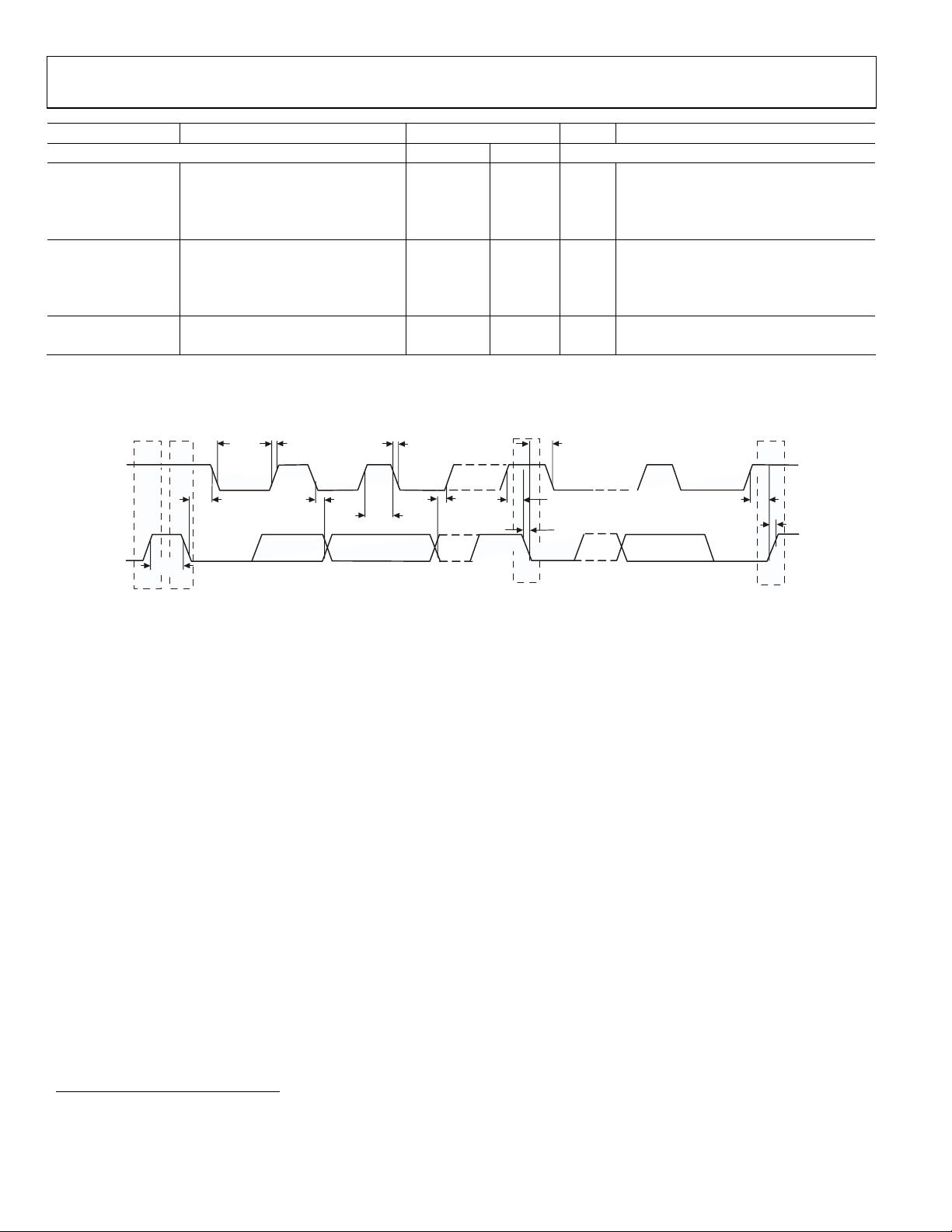
S = START CONDITION
P = STOP CONDITION
Figure 2. Two-Wire Serial Interface Timing Diagram
6
Input filtering on both the SCL and SDA inputs suppress noise spikes that are less than 50nS or 10nS for Fast Mode or High-Speed Mode respectively
Specifications subject to change without notice.
Rev. PrB 18-Feb-05| Page 6 of 22

Preliminary Technical Data AD5602/12/22
ABSOLUTE MAXIMUM RATINGS
Table 3. TA = 25°C, unless otherwise noted
Parameter Rating
VDD to GND –0.3 V to + 7.0 V
Digital Input Voltage to GND –0.3 V to VDD + 0.3 V
V
to GND –0.3 V to VDD + 0.3 V
OUT
Operating Temperature Range
Extended Automotive (W,Y Version) –40°C to +125°C
Extended industrial (A,B Version) -40°C to + 85°C
Storage Temperature Range –65°C to +160°C
Maximum Junction Temperature 150°C
SC70 Package
θJA Thermal Impedance 332°C/W
θJC Thermal Impedance 120°C/W
Lead Temperature, Soldering
Vapor Phase (60 sec) 215°C
Infrared (15 sec) 220°C
ESD 2.0 kV
ORDERING GUIDE
Stresses above those listed under Absolute Maximum Ratings
may cause permanent damage to the device. This is a stress
rating only; functional operation of the device at these or any
other conditions above those listed in the operational sections
of this specification is not implied. Exposure to absolute
maximum rating conditions for extended periods may affect
device reliability.
Model INL I2C Interface Modes Supported Temperature Range Power Supply
AD5602YKSZ-1 ± 1 LSB Max Standard , Fast and High Speed Modes -40°C to 125°C 2.7 V to 5.5V KS-6 6-Lead SC-70 D5W
AD5602BKSZ-2 ± 1 LSB Max Standard, Fast Modes -40°C to 85°C 2.7 V to 5.5V KS-6 6-Lead SC-70 D5X
AD5602YKSZ-2 ± 1 LSB Max Standard , Fast Modes -40°C to 125°C 2.7 V to 5.5V KS-6 6-Lead SC-70 D5Y
AD5612YKSZ-1 ± 0.5 LSB Max Standard , Fast and High Speed Modes -40°C to 125°C 2.7 V to 5.5V KS-6 6-Lead SC-70 D5T
AD5612BKSZ-2 ± 0.5 LSB Max Standard, Fast Modes -40°C to 85°C 2.7 V to 5.5V KS-6 6-Lead SC-70 D5U
AD5612AKSZ-2 ± 4 LSB Max Standard , Fast Modes -40°C to 85°C 2.7 V to 5.5V KS-6 6-Lead SC-70 D5V
AD5612YKSZ-2 ± 0.5 LSB Max Standard, Fast Modes -40°C to 125°C 2.7 V to 5.5V KS-6 6-Lead SC-70 D5S
AD5622YKSZ-1 ± 2 LSB Max Standard , Fast and High Speed Modes -40°C to 125°C 2.7 V to 5.5V KS-6 6-Lead SC-70 D5M
AD5622BKSZ-2 ± 2 LSB Max Standard, Fast Modes -40°C to 85°C 2.7 V to 5.5V KS-6 6-Lead SC-70 D5N
AD5622YKSZ-2 ± 2 LSB Max Standard , Fast Modes -40°C to 125°C 2.7 V to 5.5V KS-6 6-Lead SC-70 D5P
AD5622WKSZ-1 ± 6 LSB Max Standard , Fast and High Speed Modes -40°C to 125°C 2.7 V to 5.5V KS-6 6-Lead SC-70 D5Q
AD5622AKSZ-2 ± 6 LSB Max Standard, Fast Modes -40°C to 85°C 2.7 V to 5.5V KS-6 6-Lead SC-70 D5R
Range
Package
Option
Package
Description
Branding
ESD CAUTION
ESD (electrostatic discharge) sensitive device. Electrostatic charges as high as 4000 V readily accumulate on the
human body and test equipment and can discharge without detection. Although this product features
proprietary ESD protection circuitry, permanent damage may occur on devices subjected to high energy
electrostatic discharges. Therefore, proper ESD precautions are recommended to avoid performance
degradation or loss of functionality.
Rev. PrB 18-Feb-05| Page 7 of 22
 Loading...