ANALOG DEVICES AD5545 Service Manual
Serial-Input, 16-/14-Bit DACs
AD5545/AD5555
Rev. E
Trademarks and registered trademarks are the property of their respective owners.
Fax: 781.461.3113 ©2003–2011 Analog Devices, Inc. All rights reserved.
AD5545/
AD5555
V
DD
RFBA
V
REF
BV
REF
A
I
OUT
A
A
GND
A
SDI
CS
CLK
DGND MSB
RS
LDAC
DAC A
DAC A
B
D0..DX
EN
R
R
R
R
16 OR 14
ADDR
DECODE
INPUT
REGISTER
POWER-
ON
RESET
INPUT
REGISTER
DAC A
REGISTER
DAC B
REGISTER
R
FB
B
I
OUT
B
A
GND
B
DAC B
0291 8-0 -00 1
Data Sheet
FEATURES
16-bit resolution AD5545
14-bit resolution AD5555
±1 LSB DNL monotonic
±1 LSB INL
2 mA full-scale current ±20%, with V
0.5 µs settling time
2Q multiplying reference-input 6.9 MHz BW
Zero or midscale power-up preset
Zero or midscale dynamic reset
3-wire interface
Compact TSSOP-16 package
APPLICATIONS
Automatic test equipment
Instrumentation
Digitally controlled calibration
Industrial control PLCs
Programmable attenuator
PRODUCT OVERVIEW
The AD5545/AD5555 are 16-bit/14-bit, current-output, digitalto-analog converters designed to operate from a single 5 V
supply with bipolar output up to ±15 V capability.
An external reference is needed to establish the full-scale
output-current. An internal feedback resistor (R
the resistance and temperature tracking when combined
with an external op amp to complete the I-to-V conversion.
A serial data interface offers high speed, 3-wire microcontroller
compatible inputs using serial data in (SDI), clock (CLK), and
chip select (
CS
). Additional
simultaneous update operation. The internal reset logic allows
power-on preset and dynamic reset at either zero or midscale,
depending on the state of the MSB pin.
The AD5545/AD5555 are packaged in the compact TSSOP-16
package and can be operated from –40°C to +85°C.
LDAC
= 10 V
REF
FB
function allows
) enhances
Dual, Current-Output,
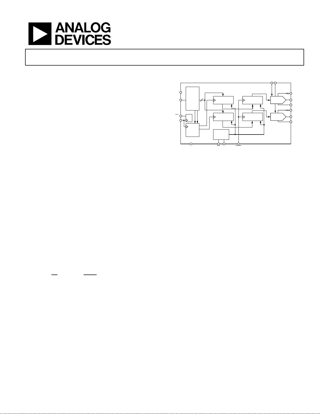
FUNCTIONAL BLOCK DIAGRAM
Figure 1.
Information furnished by Analog Devices is believed to be accurate and reliable. However, no
responsibility is assumed by Analog Devices for its use, nor for any infringements of patents or other
rights of third parties that may result from its use. Specifications subject to change without notice. No
license is granted by implication or otherwise under any patent or patent rights of Analog Devices.
One Technology Way, P.O. Box 9106, Norwood, MA 02062-9106, U.S.A.
Tel: 781.329.4700
www.analog.com

AD5545/AD5555 Data Sheet
TABLE OF CONTENTS
Features .............................................................................................. 1
Applications ....................................................................................... 1
Product Overview ............................................................................. 1
Functional Block Diagram .............................................................. 1
Revision History ............................................................................... 2
Specifications ..................................................................................... 3
Electrical Characteristics ............................................................. 3
Timing Diagrams .......................................................................... 4
Absolute Maximum Ratings ............................................................ 5
ESD Caution .................................................................................. 5
Pin Configuration and Functional Descriptions .......................... 6
Typical Performance Characteristics ............................................. 7
Theory of Operation ........................................................................ 9
Digital-to-Analog Converter ...................................................... 9
Serial Data Interface ................................................................... 10
Power-Up Sequence ................................................................... 11
Layout and Power Supply Bypassing ....................................... 11
Grounding ................................................................................... 11
Applications Information .............................................................. 12
Stability ........................................................................................ 12
Positive Voltage Output ............................................................. 12
Bipolar Output ............................................................................ 12
Programmable Current Source ................................................ 13
DAC with Programmable Input Reference Range ................ 14
Reference Selection .................................................................... 15
Amplifier Selection .................................................................... 15
Evaluation Board for the AD5545 ................................................ 17
System Demonstration Platform .............................................. 17
Operating the Evaluation Board .............................................. 17
Evaluation Board Schematics ................................................... 18
Evaluation Board Layout ........................................................... 21
Outline Dimensions ....................................................................... 23
Ordering Guide .......................................................................... 23
REVISION HISTORY
12/11—Rev. D to Rev. E
Added Figure 13; Renumbered Sequentially ................................ 8
5/11—Rev. C to Rev. D
Added Evaluation Board for the AD5545 Section, System
Demonstration Platform Section, and Operating the Evaluation
Board Section .................................................................................. 17
Added Figure 25 and Figure 26; Renumbered Sequentially ..... 17
Added Evaluation Board Schematics Section, Figure 27 .......... 18
Added Figure 28 .............................................................................. 19
Added Figure 29 .............................................................................. 20
Added Evaluation Board Layout Section, Figure 30, and
Figure 31, ......................................................................................... 21
Added Figure 32 .............................................................................. 22
Changes to Ordering Guide .......................................................... 23
3/11—Rev. B to Rev. C
Change to Equation 4, Bipolar Output Section .......................... 12
4/10—Rev. A to Rev. B
Changes to 2Q Multiplying Reference Input ................................. 1
Changes to AC Characteristics and Endnote 3 in Table 1 ........... 4
Changes to Figure 13 and Figure 15 ............................................... 8
Added Reference Selection Section, Amplifier Selection Section,
and Table 10 .................................................................................... 15
Added Table 11 and Table 12 ........................................................ 16
Changes to Ordering Guide .......................................................... 17
9/09—Rev. 0 to Rev. A
Changes to Features Section ............................................................ 1
Changes to Static Performance, Relative Accuracy, AD5545C
Parameter, Table 1 ............................................................................. 3
Moved ESD Caution.......................................................................... 5
Changes to Ordering Guide .......................................................... 16
7/03—Revision 0: Initial Version
Rev. E | Page 2 of 24

Data Sheet AD5545/AD5555
AD5545C
±1
LSB
Full-Scale Temperature Coefficient2
TCVFS
1 ppm/°C
50
MHz
Clock to CS Hold
ns
Power Supply Sensitivity
PSS
∆VDD = ±5%
0.006
%/%
SPECIFICATIONS
ELECTRICAL CHARACTERISTICS
VDD = 5 V ± 10%, I
Table 1.
Parameter Symbol Conditions Min Typ Max Unit
STATIC PERFORMANCE1
Resolution N AD5545, 1 LSB = V
AD5555, 1 LSB = V
Relative Accuracy INL AD5545B ±2 LSB
AD5555C ±1 LSB
Differential Nonlinearity DNL Monotonic ±1 LSB
Output Leakage Current I
Data = 0x0000, TA = TA Max 20 nA
Full-Scale Gain Error G
REFERENCE INPUT
V
Range V
REF
Input Resistance R
Input Capacitance2 C
ANALOG OUTPUT
Output Current I
Output Capacitance2 C
LOGIC INPUTS AND OUTPUT
Logic Input Low Voltage VIL 0.8 V
Logic Input High Voltage VIH 2.4 V
Input Leakage Current IIL 10 µA
Input Capacitance2 CIL 10 pF
INTERFACE TIMING
Clock Input Frequency f
Clock Width High tCH
Clock Width Low tCL
to Clock Setup
CS
Data Setup tDS
Data Hold tDH
Setup
LDAC
Hold t
Width
LDAC
SUPPLY CHARACTERISTICS
Power Supply Range VDD range 4.5 5.5 V
Positive Supply Current IDD Logic inputs = 0 V 10 µA
Power Dissipation P
= virtual GND, GND = 0 V, V
OUT
Data = 0x0000, TA = 25°C 10 nA
OUT
Data = full scale ±1 ±4 mV
FSE
–12 +12 V
REF
5 kΩ3
REF
5 pF
REF
Data = full scale 2 mA
OUT
Code dependent 200 pF
OUT
2, 4
CLK
t
CSS
t
CSH
t
LDS
LDH
t
LDAC
Logic inputs = 0 V 0.055 mW
DISS
= 10 V, TA = full operating temperature range, unless otherwise noted.
REF
/216 = 153 µV when V
REF
/214 = 610 µV when V
REF
= 10 V 16 Bits
REF
= 10 V 14 Bits
REF
10
10
0
10
ns
ns
ns
ns
5
ns
ns
ns
ns
50 MHz
10
5
10
10
Rev. E | Page 3 of 24
AD5545/AD5555 Data Sheet
029 18-0-003
A1SDI
CLK
CS
t
CSS
t
DS
t
DH
t
CH
t
CL
t
LDAC
t
CSH
t
LDS
t
LDH
LDAC
A0
INPUT REG LD
D1 D0D15 D14 D13 D12 D11 D10
029 18-0-004
A1SDI
CLK
CS
t
CSS
t
DS
t
DH
t
CH
t
CL
t
LDAC
t
CSH
t
LDS
t
LDH
LDAC
A0
INPUT REG LD
D1 D0D13 D12 D11 D10 D09 D08
Parameter Symbol Conditions Min Typ Max Unit
AC CHARACTERISTICS
Output Voltage Setting Time tS To ±0.1% full scale, data = zero scale to
full scale to zero scale
Reference Multiplying BW BW V
DAC Glitch Impulse Q V
Feedthrough Error V
Data = zero scale, V
OUT/VREF
= 100 mV rms, data = full scale, C1 = 5.6 pF 6.9 MHz
REF
= 0 V, data = midscale minus 1 to midscale –2 nV-s
REF
= 100 mV rms,
REF
f = 1 kHz, same channel
Digital Feedthrough Q
Total Harmonic Distortion THD V
Analog Crosstalk CTA V
CS
= logic high and f
= 5 V p-p, data = full scale, f = 1 kHz to 10 kHz –104 dB
REF
= 0 V, measure V
REFB
= 1 MHz
CLK
with V
OUTB
= 5 V p-p
REFA
sine wave, data = full scale, f = 1 kHz to 10 kHz
Output Spot Noise Voltage eN f = 1 kHz, BW = 1 Hz 12 nV/√Hz
1
All static performance tests (except I
is tied to the amplifier output. Typical values represent average readings measured at 25°C.
2
These parameters are guaranteed by design and not subject to production testing.
3
All ac characteristic tests are performed in a closed-loop system using an AD8038 I-to-V converter amplifier and the AD8065 for the THD specification.
4
All input control signals are specified with tR = tF = 2.5 ns (10% to 90% of 3 V) and timed from a voltage level of 1.5 V.
) are performed in a closed-loop system using an external precision OP1177 I-to-V converter amplifier. The AD5545 RFB terminal
OUT
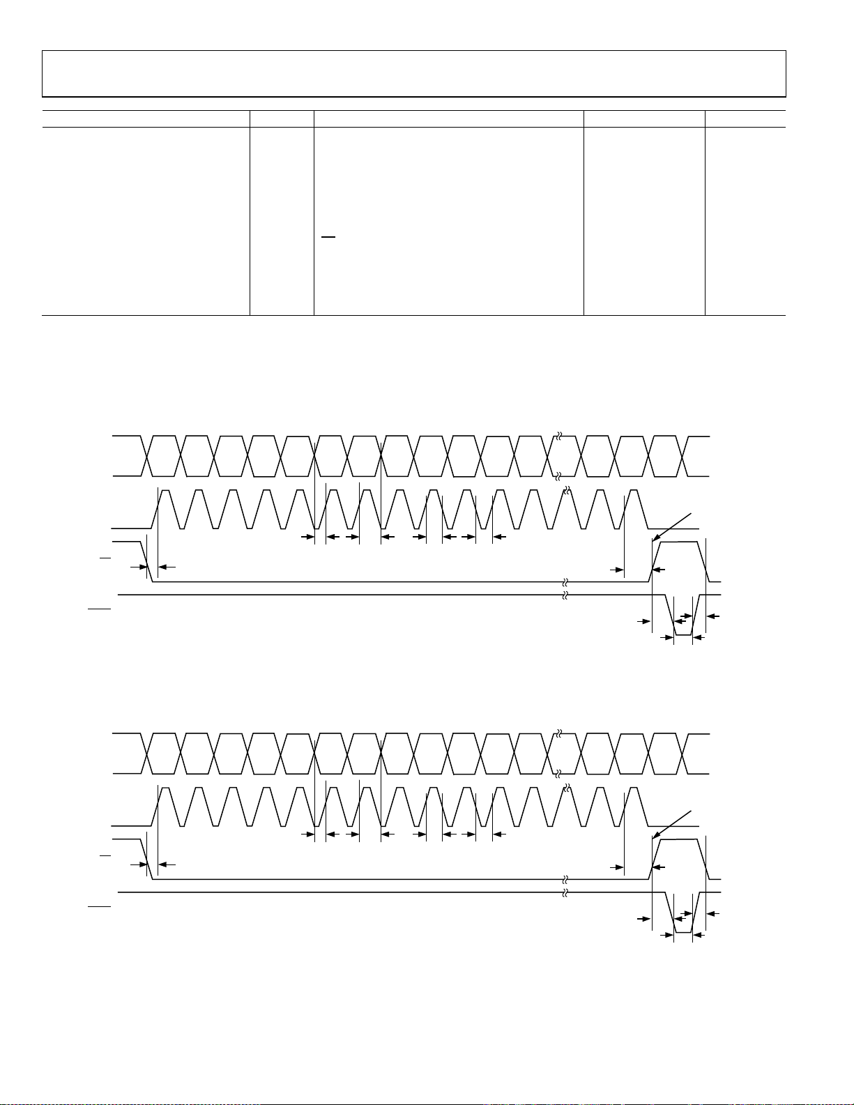
TIMING DIAGRAMS
0.5 µs
–81 dB
7
nV-s
–95 dB
Figure 2. AD5545 18-Bit Data Word Timing Diagram
Figure 3. AD5555 16-Bit Data Word Timing Diagram
Rev. E | Page 4 of 24
Data Sheet AD5545/AD5555
Package Power Dissipation
(TJ max – TA)/θJA
Thermal Resistance θJA
ABSOLUTE MAXIMUM RATINGS
Table 2.
Parameter Rating
VDD to GND –0.3 V to +8 V
V
to GND –18 V to +18 V
REF
Logic Inputs to GND –0.3 V to +8 V
V(I
) to GND –0.3 V to VDD + 0.3 V
OUT
Input Current to Any Pin except
Supplies
16-Lead TSSOP 150°C/W
Maximum Junction Temperature
max)
(T
J
Operating Temperature Range –40°C to +85°C
Storage Temperature Range –65°C to +150°C
Lead Temperature
RU-16 (Vapor Phase, 60 sec) 215°C
RU-16 (Infrared, 15 sec) 220°C
±50 mA
150°C
Stresses above those listed under Absolute Maximum Ratings
may cause permanent damage to the device. This is a stress
rating only and functional operation of the device at these or
any other conditions above those indicated in the operational
section of this specification is not implied. Exposure to absolute
maximum rating conditions for extended periods may affect
device reliability.
ESD CAUTION
Rev. E | Page 5 of 24
AD5545/AD5555 Data Sheet
AD5545/
AD5555
TOP VIEW
(Not to Scale)
8
7
6
5
1
4
3
2
9
10
11
12
16
13
14
15
CS
DGND
CLK
V
DD
MSB
LDAC
RS
SDI
V
REF
B
R
FB
B
A
GND
B
I
OUT
B
R
FB
A
A
GND
A
I
OUT
A
V
REF
A
029 18-0-002
Pin, Active Low Input. Input registers and DAC registers are set to all 0s or midscale. Register
PIN CONFIGURATION AND FUNCTIONAL DESCRIPTIONS
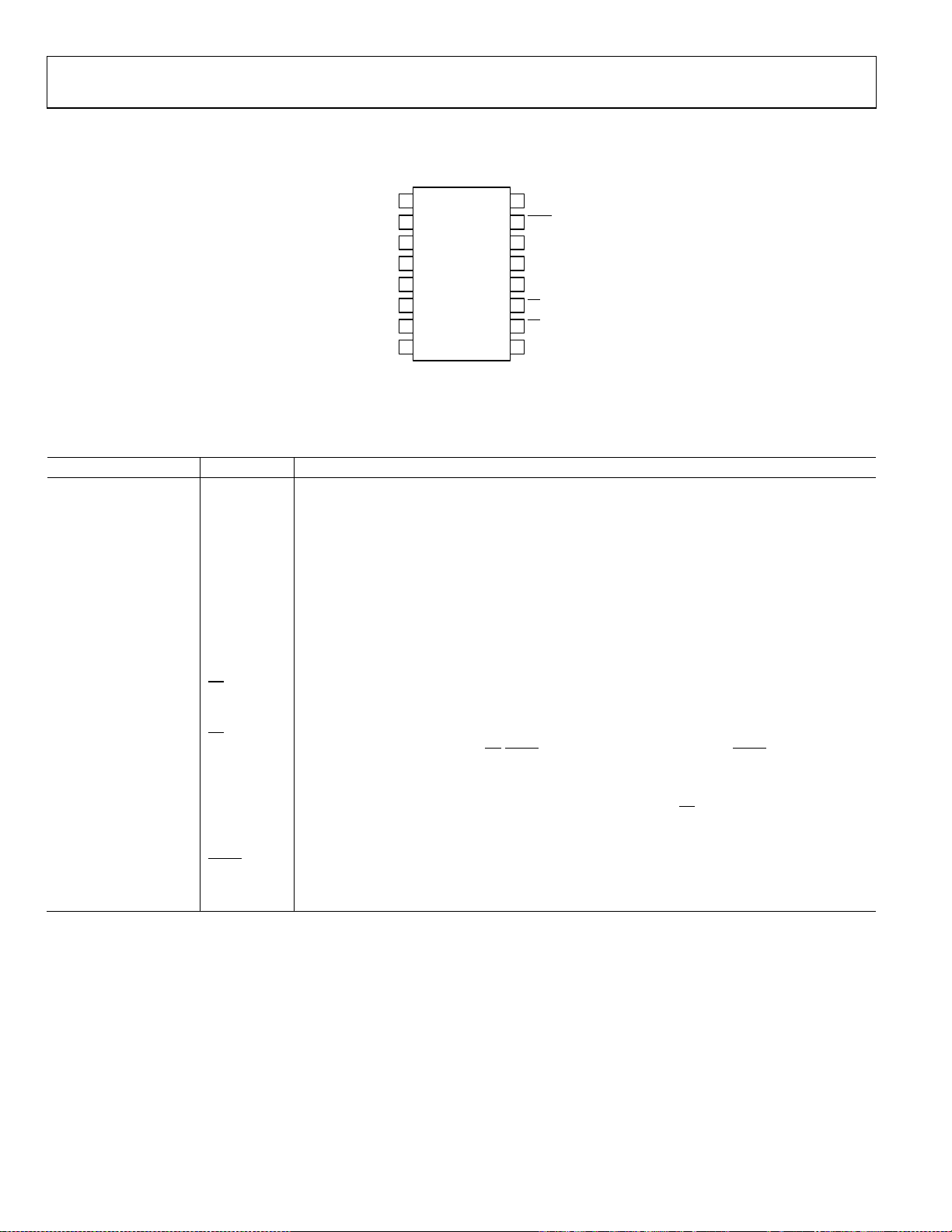
Figure 4. 16-Lead TSSOP
Table 3. Pin Function Descriptions
Pin No. Mnemonic Description
1 RFBA Establish voltage output for DAC A by connecting this pin to an external amplifier output.
2 V
3 I
4 A
5 A
6 I
7 V
A DAC A Reference Voltage Input Terminal. Establishes DAC A full-scale output voltage. This pin can
REF
A DAC A Current Output.
OUT
A DAC A Analog Ground.
GND
B DAC B Analog Ground.
GND
B DAC B Current Output.
OUT
B DAC B Reference Voltage Input Terminal. Establishes DAC B full-scale output voltage.
REF
be tied to the V
DD
pin.
This pin can be tied to the V
DD
pin.
8 RFBB Establish voltage output for DAC B by the RFBB pin connecting to an external amplifier output.
9 SDI Serial Data Input. Input data loads directly into the shift register.
10
Reset
RS
Data = 0x0000 when MSB = 0. Register Data = 0x8000 for AD5545 and 0x2000 for AD5555 when
MSB = 1.
11
Chip Select, Active Low Input. Disables shift register loading when high. Transfers serial register
CS
data to the input register when
12 DGND Digital Ground Pin.
13 VDD Positive Power Supply Input. Specified range of operation 5 V ± 10% or 3 V ± 10%.
14 MSB MSB bit sets output to either 0 or midscale during a RESET pulse (RS) or at system power-on.
Output equals zero scale when MSB = 0 and midscale when MSB = 1. MSB pin can also be tied
15
permanently to ground or V
Load DAC Register Strobe, Level Sensitive Active Low. Transfers all input register data to DAC
LDAC
.
DD
registers. Asynchronous active low input. See Table 7 and Table 8 for operation.
16 CLK Clock Input. Positive edge clocks data into shift register.
Rev. E | Page 6 of 24
CS/LDAC
returns high. This does not affect
LDAC
operation.
Data Sheet AD5545/AD5555
1.0
0.8
0.6
0 8192 16384 24576 32768 40960 49152 57344 65536
0.4
0.2
0
–0.2
–0.4
–0.6
–0.8
–1.0
INL (LSB)
CODE (Decimal)
029 18-0-009
1.0
0.8
0.6
0 8192 16384 24576 32768 40960 49152 57344 65536
0.4
0.2
0
–0.2
–0.4
–0.6
–0.8
–1.0
DNL (LSB)
CODE (Decimal)
029 18-0-010
1.0
0.8
0.6
0 2048 4096 6144
8192 10240 12288 14336 16384
0.4
0.2
0
–0.2
–0.4
–0.6
–0.8
–1.0
INL (LSB)
CODE (Decimal)
029 18-0-011
1.0
0.8
0.6
0 0248 4096 6144 8192 10240 12288 14336 16384
0.4
0.2
0
–0.2
–0.4
–0.6
–0.8
–1.0
DNL (LSB)
CODE (Decimal)
029 18-0-012
1.5
1.0
2 4
GE
DNL
INL
6 8 10
0.5
0
–0.5
–1.0
–1.5
LINEARITY ERROR (LSB)
SUPPLY VOLTAGE V
DD
(V)
V
REF
= 2.5V
T
A
= 25°C
029 18-0-013
5
4
0 0.5 1.0 1.5 2.0 3.0 3.52.5 4.0 4.5 5.0
3
2
1
0
SUPPLY CURRENT I
DD
(LSB)
LOGIC INPUT VOLTAGE V
IH
(V)
V
DD
= 5V
T
A
= 25°C
029 18-0-014
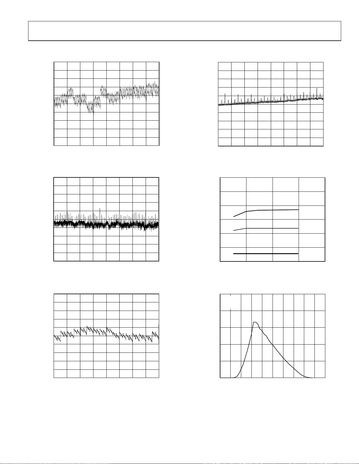
TYPICAL PERFORMANCE CHARACTERISTICS
Figure 5. AD5545 Integral Nonlinearity Error
Figure 6. AD5545 Differential Nonlinearity Error
Figure 8. AD5555 Differential Nonlinearity Error
Figure 9. Linearity Errors vs. V
DD
Figure 7. AD5555 Integral Nonlinearity Error
Figure 10. Supply Current vs. Logic Input Voltage
Rev. E | Page 7 of 24
AD5545/AD5555 Data Sheet
3.0
2.5
10k 100k 1M 10M 100M
2.0
1.5
1.0
0.5
0
SUPPLY CURRENT (mA)
CLOCK FREQUENCY (Hz)
0x5555
0x8000
0xFFFF
0x0000
029 18-0-015
90
70
10 100 1k 10k 100k 1M
50
40
60
80
30
10
20
0
PSSR (-dB)
FREQUENCY (Hz)
V
DD
= 5V ± 10%
V
REF
= 10V
029 18- 0- 01 6
02918-0-113
20
0
–20
–40
–60
–80
–100
–120
–140
–160
POWER SPECTRUM (dB)
FREQUENCY (Hz)
0 5 10 15 20 25
02918-0-117
2
–14
–12
–10
–8
–6
–4
–2
0
10k 100k 1M 10M 100M
GAIN (dB)
FREQUENCY ( Hz )
029 18-0-018
V
OUT
CS
02918-0-119
–3.70
–4.05
–4.00
–3.95
–3.90
–3.85
–3.80
–3.75
–200 4003002001000–100
V
OUT
(V)
TIME (ns)
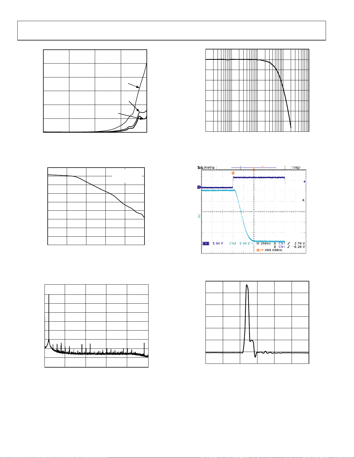
Figure 11. Supply Current vs. Clock Frequency
Figure 12. Power Supply Rejection Ration vs. Frequency
Figure 14. Reference Multiplying Bandwidth
Figure 15. Settling Time
Figure 13. AD5545/AD5555 Analog THD
Figure 16. Midscale Transition and Digital Feedthrough
Rev. E | Page 8 of 24
 Loading...