Serial-Input 16-Bit DAC
AD5544-EP
Rev. 0
Information furnished by Analog Devices is believed to be accurate and reliable. However, no
Trademarks and registered trademarks are the property of their respective owners.
Fax: 781.461.3113 ©2012 Analog Devices, Inc. All rights reserved.
INPUT
REGISTER
R
16
DAC A
REGISTER
R
2:4
DECODE
DAC A
B
C
D
POWER-ON
RESET
D0
D1
D2
D3
D4
D5
D6
D7
D8
D9
D10
D11
D12
D13
D14
D15
A0
A1
EN
V
DD
R
FB
A
I
OUT
A
A
GND
A
A
GND
F
V
SS
LDAC
MSB
RS
DGND
CLK
CS
SDI
SDO
V
REF
A
V
REF
B
V
REF
C
R
FB
B
I
OUT
B
A
GND
B
R
FB
C
I
OUT
C
A
GND
C
R
FB
D
I
OUT
D
A
GND
D
AD5544-EP
INPUT
REGISTER
R
INPUT
REGISTER
R
INPUT
REGISTER
R
DAC B
REGISTER
R
DAC C
REGISTER
R
DAC D
REGISTER
R
V
REF
D
DAC A
DAC B
DAC D
DAC C
10083-001
Enhanced Product
FEATURES
2 mA full-scale current ± 20%, with V
0.9 µs settling time to ±0.1%
12 MHz multiplying bandwidth
Midscale glitch of −1 nV-sec
Midscale or zero-scale reset
4 separate, 4-quadrant multiplying reference inputs
SPI-compatible, 3-wire interface
Double-buffered registers enable
Simultaneous multichannel change
Internal power-on reset
Compact 28-lead SSOP
ENHANCED PRODUCT FEATURES
Supports defense and aerospace applications (AQEC)
Military temperature range (−55°C to +125°C)
Controlled manufacturing baseline
1 assembly/test site
1 fabrication site
Enhanced product change notification
Qualification data available on request
= ±10 V
REF
Quad, Current-Output,
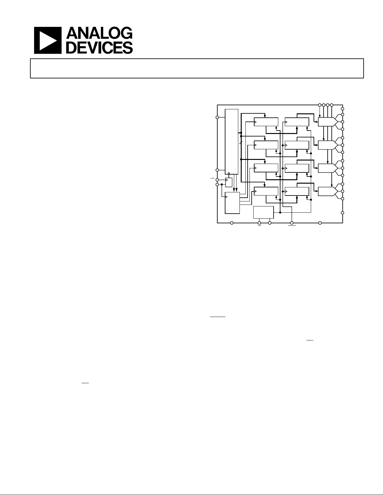
FUNCTIONAL BLOCK DIAGRAM
Figure 1.
APPLICATIONS
Automatic test equipment
Instrumentation
Digitally controlled calibration
GENERAL DESCRIPTION
The AD5544-EP quad, 16-bit, current output, digital-to-analog
converter (DAC) is designed to operate from a 2.7 V to
5.5 V supply range.
The applied external reference input voltage (V
the full-scale output current. Integrated feedback resistors (R
provide temperature-tracking, full-scale voltage outputs when
combined with an external I-to-V precision amplifier.
A double-buffered serial data interface offers high speed, 3-wire,
SPI- and microcontroller-compatible inputs using serial data in
(SDI), a chip select (
serial data out pin (SDO) allows for daisy chaining when multiple
responsibility is assumed by Analog Devices for its use, nor for any infringements of patents or other
rights of third parties that may result from its use. Specifications subject to change without notice. No
license is granted by implication or otherwise under any patent or patent rights of Analog Devices.
CS
), and clock (CLK) signals. In addition, a
REF
x) determines
FB
packages are used. A common, level-sensitive, load DAC strobe
LDAC
(
) input allows the simultaneous update of all DAC outputs
from previously loaded input registers. Additionally, an internal
power-on reset forces the output voltage to 0 at system turn-on.
)
The MSB pin allows system reset assertion (
RS
) to force all registers
to zero code when MSB = 0 or to half-scale code when MSB = 1.
The AD5544-EP is packaged in the compact 28-lead SSOP.
Additional application and technical information can be found
in the AD5544 data sheet.
One Technology Way, P.O. Box 9106, Norwood, MA 02062-9106, U.S.A.
Tel: 781.329.4700
www.analog.com

AD5544-EP Enhanced Product
TABLE OF CONTENTS
Features .............................................................................................. 1
Enhanced Product Features ............................................................ 1
Applications ....................................................................................... 1
Functional Block Diagram .............................................................. 1
General Description ......................................................................... 1
Revision History ............................................................................... 2
Specifications ..................................................................................... 3
Timing Diagrams .......................................................................... 4
REVISION HISTORY
4/12—Revision 0: Initial Version
Absolute Maximum Ratings ............................................................5
ESD Caution...................................................................................5
Pin Configuration and Function Descriptions ..............................6
Typical Performance Characteristics ..............................................8
Outline Dimensions ....................................................................... 10
Ordering Guide .......................................................................... 10
Rev. 0 | Page 2 of 12

Enhanced Product AD5544-EP
REF
REF
OUT
FSE
REF
REF
REF
REF
REF
OUT
OUT
2, 3
LDAC
LDS
LDH
DD RANGE
SS
DISS
SPECIFICATIONS
VDD = 2.7 V to 5.5 V, VSS = 0 V, I
range of −55°C to +125°C, unless otherwise noted.
Table 1.
Parameter Symbol Test Condition/Comments Min Typ Max Unit
STATIC PERFORMANCE1
Resolution N 1 LSB = V
Relative Accuracy INL ±1.5 LSB
Differential Nonlinearity DNL ±1.5 LSB
Output Leakage Current I
Data = 0x0000, TA = 85°C 20 nA
Full-Scale Gain Error G
Full-Scale Tempco2 TCVFS 1 ppm/°C
Feedback Resistor RFBx VDD = 5 V 4 6 8 kΩ
REFERENCE INPUT
V
x Range V
Input Resistance R
Input Resistance Match R
Input Capacitance2 C
ANALOG OUTPUT
Output Current I
Output Capacitance2 C
LOGIC INPUT AND OUTPUT
Logic Input Low Voltage VIL 0.8 V
Logic Input High Voltage VIH 2.4 V
Input Leakage Current IIL 1 µA
Input Capacitance2 CIL 10 pF
Logic Output Low Voltage VOL IOL = 1.6 mA 0.4 V
Logic Output High Voltage VOH IOH = 100 µA 4 V
INTERFACE TIMING
Clock Width High tCH 25 ns
Clock Width Low tCL 25 ns
to Clock Setup t
CS
Clock to CS Hold t
Clock to SDO Propagation
Delay
Load DAC Pulse Width t
Data Setup tDS 20 ns
Data Hold tDH 20 ns
Load Setup t
Load Hold t
SUPPLY CHARACTERISTICS
Power Supply Range V
Positive Supply Current IDD Logic inputs = 0 V 5 µA
Negative Supply Current ISS Logic inputs = 0 V, V
Power Dissipation P
Power Supply Sensitivity PSS ∆VDD = ±5% 0.006 %/%
x = virtual GND, A
OUT
x = 0 V, V
GND
REF
x/216 = 153 µV when V
A = V
REF
B = V
REF
C = V
D = 10 V, TA = full operating temperature
REF
= 10 V 16 Bits
x Data = 0x0000, TA = 25°C 10 nA
Data = 0xFFFF ±0.75 ±4 mV
x −15 +15 V
x 4 6 8 kΩ
x Channel-to-channel 0.35 %
x 5 pF
x Data = 0xFFFF 1.25 2.5 mA
x Code dependent 35 pF
0 ns
CSS
25 ns
CSH
tPD 2 20 ns
25 ns
5 ns
25 ns
2.7 5.5 V
= −5 V 0.001 9 µA
Logic inputs = 0 V 1.25 mW
Rev. 0 | Page 3 of 12

AD5544-EP Enhanced Product
REF
OUT
REF
REF
CLK
REF
t
LDH
t
LDS
t
LDAC
t
CSH
t
PD
t
CL
t
CH
t
DH
t
DS
t
CSS
SDI
CLK
CS
LDAC
SDO
INPUT
REG
LD
A1 A0 D15 D14 D13 D12 D11 D10 D1 D0
10083-004
Parameter Symbol Test Condition/Comments Min Typ Max Unit
AC CHARACTERISTICS4
Output Voltage Settling Time tS To ±0.1% of full scale, data = 0x0000 to 0xFFFF to 0x0000 0.9 µs
Reference Multiplying
Bandwidth (BW)
DAC Glitch Impulse Q V
Feedthrough Error V
Crosstalk Error V
Digital Feedthrough Q
Total Harmonic Distortion THD V
Output Spot Noise Voltage eN f = 1 kHz, BW = 1 Hz 7 nV/√Hz
1
All static performance tests (except I
is tied to the amplifier output. Typical values represent average readings measured at 25°C.
2
These parameters are guaranteed by design and not subject to production testing.
3
All input control signals are specified with tR = tF = 2.5 ns (10% to 90% of 3 V) and timed from a voltage level of 1.5 V.
4
All ac characteristic tests are performed in a closed-loop system using an AD8038 I-to-V converter amplifier.
TIMING DIAGRAMS
BW − 3 dB V
x = 5 V p-p, data = 0xFFFF, CFB = 2.0 pF, 12 MHz
REF
x = 8 V, data = 0x0000 to 0x8000 to 0x0000 −1 nV-sec
x/V
x Data = 0x0000, V
A/V
OUT
B Data = 0x0000, V
REF
x = 100 mV rms, f = 100 kHz −65 dB
B = 100 mV rms, adjacent channel,
REF
−90 dB
f = 100 kHz
= 1, f
CS
= 1 MHz 0.6 nV-sec
x = 5 V p-p, data = 0xFFFF, f = 1 kHz −98 dB
x) are performed in a closed-loop system using an external precision OP177 I-to-V converter amplifier. The AD5544 RFB terminal
OUT
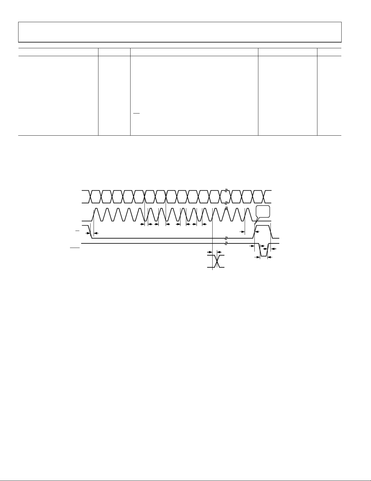
Figure 2. Timing Diagram
Rev. 0 | Page 4 of 12
 Loading...