Quad, Current-Output,
FEATURES
AD5544 16-bit resolution
AD5554 14-bit resolution
2 mA full-scale current ±20%, with V
2 µs settling time
BIAS for zero-scale error reduction @ temp
V
SS
midscale or zero-scale reset
Four separate, 4-Q multiplying reference inputs
®-compatible 3-wire interface
SPI
Double buffered registers enable
Simultaneous multichannel change
Internal power ON reset
Compact SSOP-28 package
APPLICATIONS
Automatic test equipment
Instrumentation
Digitally controlled calibration
GENERAL DESCRIPTION
The AD5544/AD5554 quad, 16-/14-bit, current-output, digital
to-analog converters are designed to operate from a single
5 V supply.
The applied external reference input voltage (V
the full-scale output current. Integrated feedback resistors (R
provide temperature-tracking, full-scale voltage outputs when
combined with an external I-to-V precision amplifier.
A double-buffered serial-data interface offers high speed,
3-wire, SPI- and microcontroller-compatible inputs using serial-
CS
data-in (SDI), a chip-select (
addition, a serial-data-out pin (SDO) allows for daisy-chaining
when multiple packages are used. A common, level-sensitive,
load-DAC strobe (
LDAC
of all DAC outputs from previously loaded input registers.
Additionally, an internal power ON reset forces the output
voltage to zero at system turn ON. An MSB pin allows system
reset assertion (
RS
) to force all registers to zero code when
MSB = 0, or to half-scale code when MSB = 1.
The AD5544/AD5554 are packaged in the compact SSOP-28.
), and clock (CLK) signals. In
) input allows the simultaneous update
= ±10 V
REF
) determines
REF
FB
Serial-Input 16-/14-Bit DACs
AD5544/AD5554
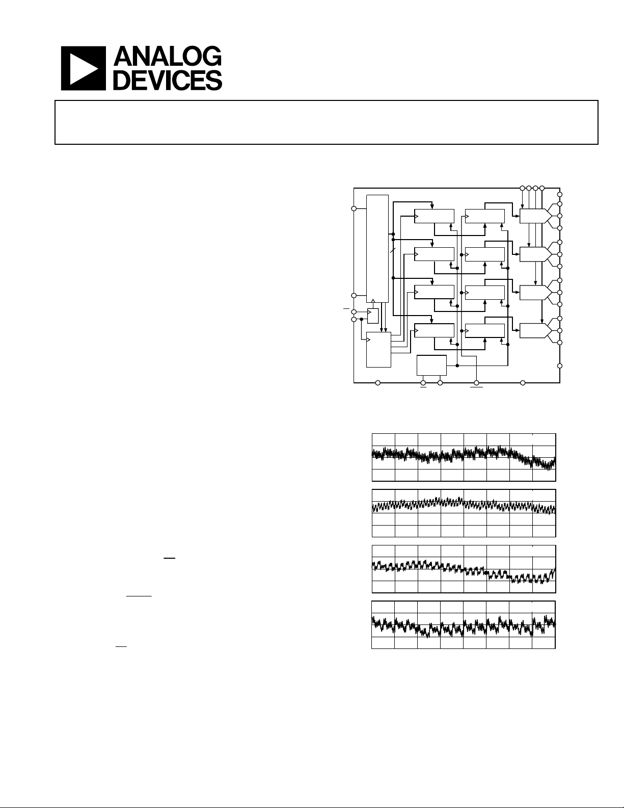
FUNCTIONAL BLOCK DIAGRAM
V
ABC
D
REF
V
D0
D10
D11
D12
D13
D14
D15
EN
DAC A
2:4
DECODE
D1
D2
D3
D4
D5
D6
D7
D8
16
D9
A0
A1
B
C
D
INPUT
REGISTER
INPUT
REGISTER
INPUT
REGISTER
INPUT
REGISTER
POWER-
ON
RESET
MSBRSDGND
DAC A
REGISTER
R
DAC B
REGISTER
R
DAC C
REGISTER
R
DAC D
REGISTER
R
LDAC
DAC A
R
DAC B
R
DAC C
R
DAC D
R
AD5544
V
SS
SDO
CLK
SDI
CS
Figure 1.
1.0
0.5
0
–0.5
–1.0
INL (LSB)
1.0
0.5
0
–0.5
–1.0
1.0
0.5
0
–0.5
–1.0
1.0
0.5
0
–0.5
–1.0
CODE (Decimal)
)
Figure 2. AD5544 INL vs. Code Plot ( TA = 25°C)
DAC A
DAC B
DAC C
DAC D
57344491524096032768245761638481920 65536
DD
RFBA
I
OUT
A
GND
R
FB
I
OUT
A
GND
R
FB
I
OUT
A
GND
R
FB
I
OUT
A
GND
A
GND
A
A
B
B
B
C
C
C
D
D
D
F
00943-0-001
00943-0-002
Rev. A
Information furnished by Analog Devices is believed to be accurate and reliable.
However, no responsibility is assumed by Analog Devices for its use, nor for any
infringements of patents or other rights of third parties that may result from its use.
Specifications subject to change without notice. No license is granted by implication
or otherwise under any patent or patent rights of Analog Devices. Trademarks and
registered trademarks are the property of their respective owners.
One Technology Way, P.O. Box 9106, Norwood, MA 02062-9106, U.S.A.
Tel: 781.329.4700
Fax: 781.326.8703 © 2004 Analog Devices, Inc. All rights reserved.
www.analog.com

AD5554/AD5554
TABLE OF CONTENTS
Specifications..................................................................................... 3
AD5544 Electrical Characteristics ............................................. 3
AD5554 Electrical Characteristics ............................................. 4
Absolute Maximum Ratings............................................................ 6
ESD Caution.................................................................................. 6
Pin Configuration and Function Descriptions............................. 7
Typical Performance Characteristics........................................... 10
REVISION HISTORY
12/04—Rev. 0 to Rev. A
Updated Format...................................................................... Universal
Change to Electrical Characteristics Tables .......................................4
Change to Pin Description Table.......................................................10
Addition of Power Supply Sequence Section...................................19
Addition of Layout and Power Supply Bypassing Section.............19
Addition of Grounding Section.........................................................19
Addition of Figure 32..........................................................................19
Circuit Operation ........................................................................... 14
D/A Converter............................................................................ 14
Serial Data Interface....................................................................... 16
Power On Reset .......................................................................... 17
Applications ................................................................................ 17
Outline Dimensions....................................................................... 18
Ordering Guide .......................................................................... 18
4/00—Revision 0: Initial Version
Rev. A | Page 2 of 20

AD5544/AD5554
SPECIFICATIONS
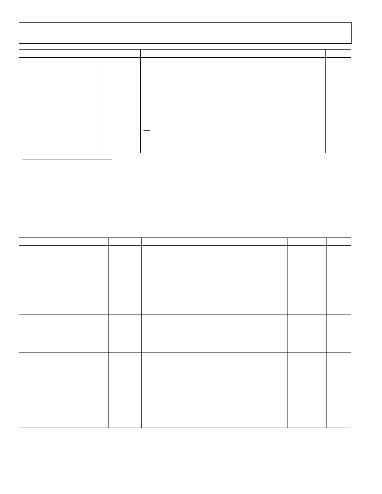
AD5544 ELECTRICAL CHARACTERISTICS
VDD = 5 V ±10%, VSS = 0 V, I
otherwise noted.
Table 1.
Parameter Symbol Condition Min Typ Max Unit
STATIC PERFORMANCE
1
Resolution N 1 LSB = V
Relative Accuracy INL ±4 LSB
Differential Nonlinearity DNL ±1.5 LSB
Output Leakage Current I
I
Full-Scale Gain Error G
Full-Scale Tempco
2
Feedback Resistor RFBX VDD = 5 V 4 6 8 kΩ
REFERENCE INPUT
V
X Range V
REF
Input Resistance R
Input Resistance Match R
Input Capacitance2 C
ANALOG OUTPUT
Output Current I
Output Capacitance2 C
LOGIC INPUT AND OUTPUT
Logic Input Low Voltage V
Logic Input High Voltage V
Input Leakage Current I
Input Capacitance2 CIL 10 pF
Logic Output Low Voltage V
Logic Output High Voltage V
INTERFACE TIMING
2, 3
Clock Width High t
Clock Width Low t
CS
to Clock Setup
Clock to CS Hold
Clock to SDO Prop Delay t
Load DAC Pulse Width t
Data Setup t
Data Hold t
Load Setup t
Load Hold t
SUPPLY CHARACTERISTICS
Power Supply Range V
Positive Supply Current I
Negative Supply Current I
Power Dissipation P
Power Supply Sensitivity PSS ∆VDD = ±5% 0.006 %/%
X = virtual GND, A
OUT
X = 0 V, V
GND
A, B, C, D = 10 V, TA = full operating temperature range, unless
REF
/216 = 153 µV when V
REF
X Data = 0000H, TA = 25°C 10 nA
OUT
X Data = 0000H, TA = TA max 20 nA
OUT
FSE
TCV
FS
X −15 +15 V
REF
X 4 6 8 kΩ
REF
X Channel-to-channel 1 %
REF
X 5 pF
REF
X Data = FFFF
OUT
X Code-dependent 80 pF
OUT
IL
IH
IL
OL
OH
Data = FFFF
H
1 ppm/°C
H
0.8 V
2.4 V
1 µA
IOL = 1.6 mA 0.4 V
IOH = 100 µA 4 V
= 10 V 16 Bits
REF
±0.75 ±3 mV
1.25 2.5 mA
CH
CL
t
CSS
t
CSH
PD
LDAC
DS
DH
LDS
LDH
DD RANGE
DD
SS
DISS
25 ns
25 ns
0 ns
25 ns
2 20 ns
25 ns
20 ns
20 ns
5 ns
25 ns
4.5 5.5 V
Logic inputs = 0 V 50 250 µA
Logic inputs = 0 V, V
= –5 V 0.001 1 µA
SS
Logic inputs = 0 V 1.25 mW
Rev. A | Page 3 of 20

AD5554/AD5554
Parameter Symbol Condition Min Typ Max Unit
AC CHARACTERISTICS
Output Voltage Settling Time t
Output Voltage Settling Time
Reference Multiplying BW BW − 3 dB V
DAC Glitch Impulse Q V
Feedthrough Error V
Crosstalk Error V
Digital Feedthrough Q
Total Harmonic Distortion THD V
Output Spot Noise Voltage e
1
All static performance tests (except I
tied to the amplifier output. Typical values represent average readings measured at 25 °C.
2
These parameters are guaranteed by design and not subject to production testing.
3
All input control signals are specified with tR = tF = 2.5 ns (10% to 90% of 3 V) and timed from a voltage level of 1.5 V.
4
All ac characteristic tests are performed in a closed-loop system using an OP42 I-to-V converter amplifier.
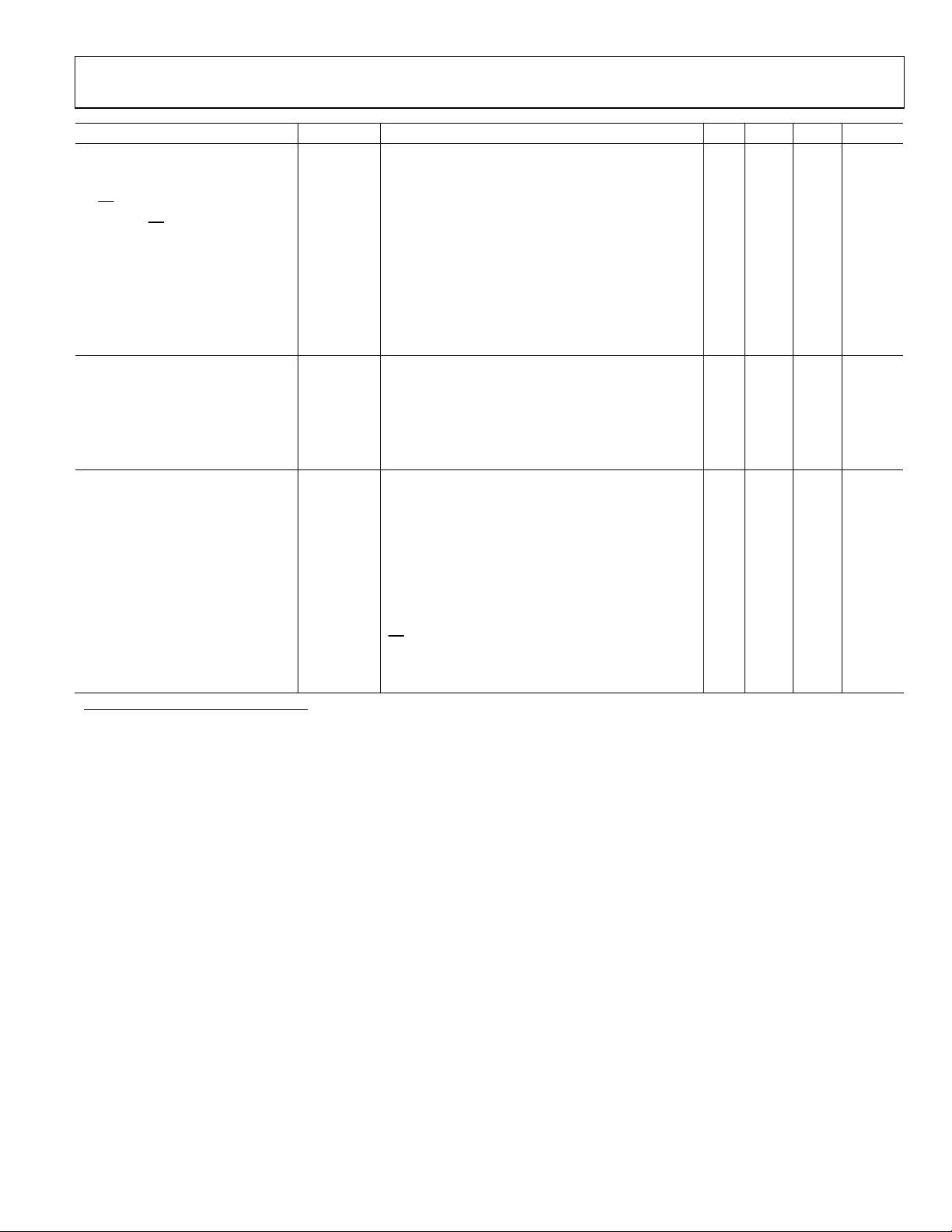
AD5554 ELECTRICAL CHARACTERISTICS
VDD = 5 V ±10%, V
otherwise noted.
Table 2.
Parameter Symbol Condition Min Typ Max Unit
STATIC PERFORMANCE
Resolution N 1 LSB = V
Relative Accuracy INL ±1 LSB
Differential Nonlinearity DNL ±1 LSB
Output Leakage Current I
I
Full-Scale Gain Error G
Full-Scale Tempco
Feedback Resistor RFBX VDD = 5 V 4 6 8 kΩ
REFERENCE INPUT
V
X Range V
REF
Input Resistance R
Input Resistance Match R
Input Capacitance2 C
ANALOG OUTPUT
Output Current
Output Capacitance
LOGIC INPUT AND OUTPUT
Logic Input Low Voltage V
Logic Input High Voltage V
Input Leakage Current I
Input Capacitance2 CIL 10 pF
Logic Output Low Voltage V
Logic Output High Voltage V
4
= 0 V, I
SS
2
S
To ±0.1% of full scale, data = 0000H to FFFFH to
1 µs
0x0000
t
S
X/V
OUT
REF
A/V
OUT
REF
To ±0.0015% of full scale, data = 0000H to FFFFH to
0000
H
X = 100 mV rms, data = FFFFH, CFB = 15 pF 2 MHz
REF
X = 10 V, data 0000H to 8000H to 0000
REF
X Data = 0000H, V
B
Data = 0000
X = 100 mV rms, f = 100 kHz −65 dB
REF
, V
B = 100 mV rms, adjacent
H
REF
H
2
µs
12 nV-s
−90 dB
channel, f = 100 kHz
CS
= 1, and f
= 5 V p-p, data = FFFFH, f = 1 kHz −90 dB
REF
N
) are performed in a closed-loop system using an external precision OP177 I-to-V converter amplifier. The AD5544 RFB terminal is
OUT
X = virtual GND, A
OUT
1
2
X Data = 0000H, TA = 25°C 10 nA
OUT
X Data = 0000H, TA = TA Max 20 nA
OUT
FSE
TCV
FS
X −15 +15 V
REF
X 4 6 8 kΩ
REF
X Channel-to-channel 1 %
REF
X 5 pF
REF
X
I
OUT
C
X
OUT
IL
IH
IL
OL
OH
f = 1 kHz, BW = 1 Hz 7 nV√Hz
X = 0 V, V
GND
Data = 3FFF
1 ppm/°C
Data = 3FFF
Code-dependent
0.8 V
2.4 V
1 µA
IOL = 1.6 mA 0.4 V
IOH = 100 µA 4 V
= 1 MHz
CLK
A, B, C, D = 10 V, TA = full operating temperature range, unless
REF
/214 = 610 µV when V
REF
H
H
= 10 V 14 Bits
REF
5 nV-s
±2 ±10 mV
1.25
80
2.5
mA
pF
Rev. A | Page 4 of 20

AD5544/AD5554
Parameter Symbol Condition Min Typ Max Unit
INTERFACE TIMING
Clock Width High t
Clock Width Low t
CS
to Clock Setup
Clock to CS Hold
Clock to SDO Prop Delay t
Load DAC Pulse Width t
Data Setup t
Data Hold t
Load Setup t
Load Hold t
SUPPLY CHARACTERISTICS
Power Supply Range V
Positive Supply Current I
Negative Supply Current I
Power Dissipation P
Power Supply Sensitivity PSS ∆VDD = ±5% 0.006 %/%
AC CHARACTERISTICS
Output Voltage Settling Time t
Output Voltage Settling Time t
Reference Multiplying BW BW – 3 dB V
DAC Glitch Impulse Q V
Feedthrough Error V
Crosstalk Error V
Digital Feedthrough Q
Total Harmonic Distortion THD V
Output Spot Noise Voltage e
1
All static performance tests (except I
tied to the amplifier output. Typical values represent average readings measured at 25°C.
2
These parameters are guaranteed by design and not subject to production testing.
3
All input control signals are specified with tR = tF = 2.5 ns (10% to 90% of 3 V) and timed from a voltage level of 1.5 V.
4
All ac characteristic tests are performed in a closed-loop system using an OP42 I-to-V converter amplifier.
2, 3
4
CH
CL
t
CSS
t
CSH
PD
LDAC
DS
DH
LDS
LDH
DD RANGE
DD
SS
DISS
25 ns
25 ns
0 ns
25 ns
2 20 ns
25 ns
20 ns
20 ns
5 ns
25 ns
4.5 5.5 V
Logic inputs = 0 V 50 250 µA
Logic inputs = 0 V, VSS = –5 V 0.001 1 µA
Logic inputs = 0 V 1.25 mW
S
S
X/V
OUT
A/V
OUT
To ±0.1% of full scale, data = 0000H to 3FFFH to 0000H 1 µs
To ±0.0015% of full scale, data = 0000H to 3FFF
to 0000
H
X = 100 mV rms, data = 3FFFH, CFB = 15 pF 2 MHz
REF
X = 10 V, data 0000H to 2000H to 0000
REF
X Data = 0000H, V
REF
B
Data = 0000
REF
X = 100 mV rms, f = 100 kHz –65 dB
REF
, V
B = 100 mV rms, adjacent channel,
H
REF
H
H
2 µs
12 nV-s
–90 dB
f = 100 kHz
CS
= 1, and f
= 5 V p-p, data = 3FFFH, f = 1 kHz –90 dB
REF
N
) are performed in a closed-loop system using an external precision OP177 I-to-V converter amplifier. The AD5554 RFB terminal is
OUT
f = 1 kHz, BW = 1 Hz 7 nV√Hz
= 1 MHz
CLK
5 nV-s
Rev. A | Page 5 of 20

AD5554/AD5554
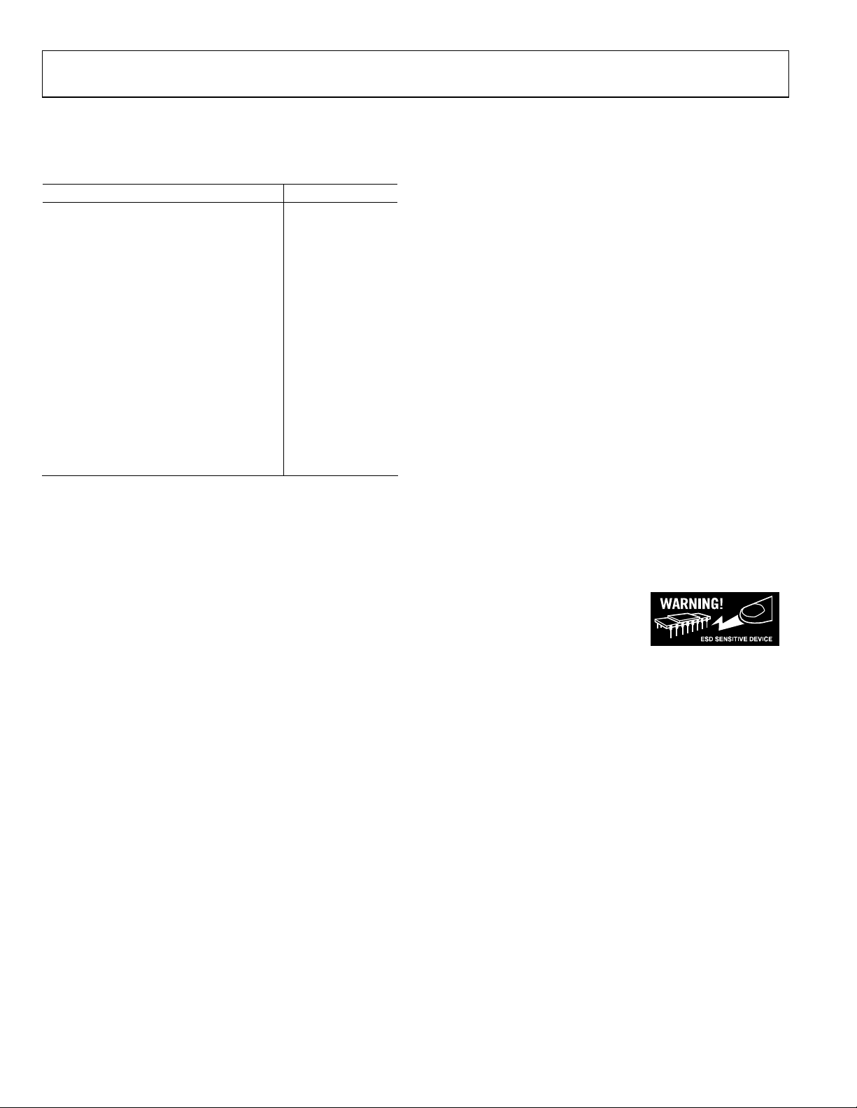
ABSOLUTE MAXIMUM RATINGS
Table 3.
Parameter Rating
VDD to GND −0.3 V, +8 V
VSS to GND +0.3 V, −7 V
V
to GND −18 V, +18 V
REF
Logic Input and Output to GND −0.3 V, +8 V
V(I
) to GND −0.3 V, VDD+ 0.3 V
OUT
A
X to DGND −0.3 V, + 0.3 V
GND
Input Current to Any Pin Except Supplies ±50 mA
Package Power Dissipation (TJ Max − TA)/θ
Thermal Resistance θ
28-Lead Shrink Surface-Mount (RS-28) 100°C/W
Maximum Junction Temperature (TJ Max) 150°C
Operating Temperature Range: Model A −40°C to +85°C
Storage Temperature Range −65°C to +150°C
Lead Temperature:
RS-28 (Vapor Phase, 60 secs) 215°C
RS-28 (Infrared, 15 secs) 220°C
JA
JA
Stresses above those listed under Absolute Maximum Ratings
may cause permanent damage to the device. This is a stress
rating only; functional operation of the device at these or any
other conditions above those indicated in the operational
sections of this specification is not implied. Exposure to
absolute maximum rating conditions for extended periods may
affect device reliability.
ESD CAUTION
ESD (electrostatic discharge) sensitive device. Electrostatic charges as high as 4000 V readily accumulate on
the human body and test equipment and can discharge without detection. Although this product features
proprietary ESD protection circuitry, permanent damage may occur on devices subjected to high energy
electrostatic discharges. Therefore, proper ESD precautions are recommended to avoid performance
degradation or loss of functionality.
Rev. A | Page 6 of 20
 Loading...