


 Loading...
MAX V Device Handbook
101 Innovation Drive San Jose, CA 95134 www.altera.com
Subscribe

© 2011 Altera Corporation. All rights reserved. ALTERA, ARRIA, CYCLONE, HARDCOPY, MAX, MEGACORE, NIOS, QUARTUS and STRATIX are Reg. U.S. Pat. & Tm. Off. and/or trademarks of Altera Corporation in the U.S. and other countries. All other trademarks and service marks are the property of their respective holders as described at www.altera.com/common/legal.html. Altera warrants performance of its semiconductor products to current specifications in accordance with Altera’s standard warranty, but reserves the right to make changes to any products and services at any time without notice. Altera assumes no responsibility or liability arising out of the application or use of any information, product, or service described herein except as expressly agreed to in writing by Altera. Altera customers are advised to obtain the latest version of device specifications before relying on any published information and before placing orders for products or services.
MAX V Device Handbook |
May 2011 Altera Corporation |

Contents
Section I. MAX V Device Core
Chapter 1. MAX V Device Family Overview
Feature Summary . . . . . . . . . . . . . . . . . . . . . . . . . . . . . . . . . . . . . . . . . . . . . . . . . . . . . . . . . . . . . . . . . . . . . . . 1–1
Integrated Software Platform . . . . . . . . . . . . . . . . . . . . . . . . . . . . . . . . . . . . . . . . . . . . . . . . . . . . . . . . . . . . . 1–3
Device Pin-Outs . . . . . . . . . . . . . . . . . . . . . . . . . . . . . . . . . . . . . . . . . . . . . . . . . . . . . . . . . . . . . . . . . . . . . . . . . 1–3
Ordering Information . . . . . . . . . . . . . . . . . . . . . . . . . . . . . . . . . . . . . . . . . . . . . . . . . . . . . . . . . . . . . . . . . . . . 1–4
Document Revision History . . . . . . . . . . . . . . . . . . . . . . . . . . . . . . . . . . . . . . . . . . . . . . . . . . . . . . . . . . . . . . 1–4
Chapter 2. MAX V Architecture
Functional Description . . . . . . . . . . . . . . . . . . . . . . . . . . . . . . . . . . . . . . . . . . . . . . . . . . . . . . . . . . . . . . . . . . . 2–1 Logic Array Blocks . . . . . . . . . . . . . . . . . . . . . . . . . . . . . . . . . . . . . . . . . . . . . . . . . . . . . . . . . . . . . . . . . . . . . . 2–4 LAB Interconnects . . . . . . . . . . . . . . . . . . . . . . . . . . . . . . . . . . . . . . . . . . . . . . . . . . . . . . . . . . . . . . . . . . . . 2–6 LAB Control Signals . . . . . . . . . . . . . . . . . . . . . . . . . . . . . . . . . . . . . . . . . . . . . . . . . . . . . . . . . . . . . . . . . . . 2–6 Logic Elements . . . . . . . . . . . . . . . . . . . . . . . . . . . . . . . . . . . . . . . . . . . . . . . . . . . . . . . . . . . . . . . . . . . . . . . . . . 2–8 LUT Chain and Register Chain . . . . . . . . . . . . . . . . . . . . . . . . . . . . . . . . . . . . . . . . . . . . . . . . . . . . . . . . . . 2–9 addnsub Signal . . . . . . . . . . . . . . . . . . . . . . . . . . . . . . . . . . . . . . . . . . . . . . . . . . . . . . . . . . . . . . . . . . . . . . . 2–9 LE Operating Modes . . . . . . . . . . . . . . . . . . . . . . . . . . . . . . . . . . . . . . . . . . . . . . . . . . . . . . . . . . . . . . . . . . 2–9 Normal Mode . . . . . . . . . . . . . . . . . . . . . . . . . . . . . . . . . . . . . . . . . . . . . . . . . . . . . . . . . . . . . . . . . . . . . 2–10 Dynamic Arithmetic Mode . . . . . . . . . . . . . . . . . . . . . . . . . . . . . . . . . . . . . . . . . . . . . . . . . . . . . . . . . . 2–10 Carry-Select Chain . . . . . . . . . . . . . . . . . . . . . . . . . . . . . . . . . . . . . . . . . . . . . . . . . . . . . . . . . . . . . . . . . 2–11 Clear and Preset Logic Control . . . . . . . . . . . . . . . . . . . . . . . . . . . . . . . . . . . . . . . . . . . . . . . . . . . . . . 2–13 LE RAM . . . . . . . . . . . . . . . . . . . . . . . . . . . . . . . . . . . . . . . . . . . . . . . . . . . . . . . . . . . . . . . . . . . . . . . . . . . . 2–13
MultiTrack Interconnect . . . . . . . . . . . . . . . . . . . . . . . . . . . . . . . . . . . . . . . . . . . . . . . . . . . . . . . . . . . . . . . . . 2–14 Global Signals . . . . . . . . . . . . . . . . . . . . . . . . . . . . . . . . . . . . . . . . . . . . . . . . . . . . . . . . . . . . . . . . . . . . . . . . . 2–19 User Flash Memory Block . . . . . . . . . . . . . . . . . . . . . . . . . . . . . . . . . . . . . . . . . . . . . . . . . . . . . . . . . . . . . . . 2–21 UFM Storage . . . . . . . . . . . . . . . . . . . . . . . . . . . . . . . . . . . . . . . . . . . . . . . . . . . . . . . . . . . . . . . . . . . . . . . . 2–22 Internal Oscillator . . . . . . . . . . . . . . . . . . . . . . . . . . . . . . . . . . . . . . . . . . . . . . . . . . . . . . . . . . . . . . . . . . . . 2–22 Program, Erase, and Busy Signals . . . . . . . . . . . . . . . . . . . . . . . . . . . . . . . . . . . . . . . . . . . . . . . . . . . . . . 2–23 Auto-Increment Addressing . . . . . . . . . . . . . . . . . . . . . . . . . . . . . . . . . . . . . . . . . . . . . . . . . . . . . . . . . . . 2–23 Serial Interface . . . . . . . . . . . . . . . . . . . . . . . . . . . . . . . . . . . . . . . . . . . . . . . . . . . . . . . . . . . . . . . . . . . . . . . 2–23 UFM Block to Logic Array Interface . . . . . . . . . . . . . . . . . . . . . . . . . . . . . . . . . . . . . . . . . . . . . . . . . . . . 2–24 Core Voltage . . . . . . . . . . . . . . . . . . . . . . . . . . . . . . . . . . . . . . . . . . . . . . . . . . . . . . . . . . . . . . . . . . . . . . . . . . . 2–25 I/O Structure . . . . . . . . . . . . . . . . . . . . . . . . . . . . . . . . . . . . . . . . . . . . . . . . . . . . . . . . . . . . . . . . . . . . . . . . . . 2–26 Fast I/O Connection . . . . . . . . . . . . . . . . . . . . . . . . . . . . . . . . . . . . . . . . . . . . . . . . . . . . . . . . . . . . . . . . . . 2–27 I/O Blocks . . . . . . . . . . . . . . . . . . . . . . . . . . . . . . . . . . . . . . . . . . . . . . . . . . . . . . . . . . . . . . . . . . . . . . . . . . 2–28 I/O Standards and Banks . . . . . . . . . . . . . . . . . . . . . . . . . . . . . . . . . . . . . . . . . . . . . . . . . . . . . . . . . . . . . 2–29 PCI Compliance . . . . . . . . . . . . . . . . . . . . . . . . . . . . . . . . . . . . . . . . . . . . . . . . . . . . . . . . . . . . . . . . . . . 2–32 LVDS and RSDS Channels . . . . . . . . . . . . . . . . . . . . . . . . . . . . . . . . . . . . . . . . . . . . . . . . . . . . . . . . . . 2–32 Schmitt Trigger . . . . . . . . . . . . . . . . . . . . . . . . . . . . . . . . . . . . . . . . . . . . . . . . . . . . . . . . . . . . . . . . . . . . . . 2–32 Output Enable Signals . . . . . . . . . . . . . . . . . . . . . . . . . . . . . . . . . . . . . . . . . . . . . . . . . . . . . . . . . . . . . . . . 2–33 Programmable Drive Strength . . . . . . . . . . . . . . . . . . . . . . . . . . . . . . . . . . . . . . . . . . . . . . . . . . . . . . . . . 2–33 Slew-Rate Control . . . . . . . . . . . . . . . . . . . . . . . . . . . . . . . . . . . . . . . . . . . . . . . . . . . . . . . . . . . . . . . . . . . . 2–34 Open-Drain Output . . . . . . . . . . . . . . . . . . . . . . . . . . . . . . . . . . . . . . . . . . . . . . . . . . . . . . . . . . . . . . . . . . 2–34 Programmable Ground Pins . . . . . . . . . . . . . . . . . . . . . . . . . . . . . . . . . . . . . . . . . . . . . . . . . . . . . . . . . . . 2–34 Bus-Hold . . . . . . . . . . . . . . . . . . . . . . . . . . . . . . . . . . . . . . . . . . . . . . . . . . . . . . . . . . . . . . . . . . . . . . . . . . . 2–34 Programmable Pull-Up Resistor . . . . . . . . . . . . . . . . . . . . . . . . . . . . . . . . . . . . . . . . . . . . . . . . . . . . . . . . 2–35 Programmable Input Delay . . . . . . . . . . . . . . . . . . . . . . . . . . . . . . . . . . . . . . . . . . . . . . . . . . . . . . . . . . . . 2–35
May 2011 Altera Corporation |
MAX V Device Handbook |
iv |
Contents |
|
|
MultiVolt I/O Interface . . . . . . . . . . . . . . . . . . . . . . . . . . . . . . . . . . . . . . . . . . . . . . . . . . . . . . . . . . . . . . . 2–35
Document Revision History . . . . . . . . . . . . . . . . . . . . . . . . . . . . . . . . . . . . . . . . . . . . . . . . . . . . . . . . . . . . . 2–36
Chapter 3. DC and Switching Characteristics for MAX V Devices
Operating Conditions . . . . . . . . . . . . . . . . . . . . . . . . . . . . . . . . . . . . . . . . . . . . . . . . . . . . . . . . . . . . . . . . . . . |
. 3–1 |
Absolute Maximum Ratings . . . . . . . . . . . . . . . . . . . . . . . . . . . . . . . . . . . . . . . . . . . . . . . . . . . . . . . . . . . . |
3–1 |
Recommended Operating Conditions . . . . . . . . . . . . . . . . . . . . . . . . . . . . . . . . . . . . . . . . . . . . . . . . . . . . |
3–2 |
Programming/Erasure Specifications . . . . . . . . . . . . . . . . . . . . . . . . . . . . . . . . . . . . . . . . . . . . . . . . . . . . |
3–3 |
DC Electrical Characteristics . . . . . . . . . . . . . . . . . . . . . . . . . . . . . . . . . . . . . . . . . . . . . . . . . . . . . . . . . . . . |
3–3 |
Output Drive Characteristics . . . . . . . . . . . . . . . . . . . . . . . . . . . . . . . . . . . . . . . . . . . . . . . . . . . . . . . . . . . |
3–5 |
I/O Standard Specifications . . . . . . . . . . . . . . . . . . . . . . . . . . . . . . . . . . . . . . . . . . . . . . . . . . . . . . . . . . . . |
3–5 |
Bus Hold Specifications . . . . . . . . . . . . . . . . . . . . . . . . . . . . . . . . . . . . . . . . . . . . . . . . . . . . . . . . . . . . . . . . |
3–8 |
Power-Up Timing . . . . . . . . . . . . . . . . . . . . . . . . . . . . . . . . . . . . . . . . . . . . . . . . . . . . . . . . . . . . . . . . . . . . . |
3–9 |
Power Consumption . . . . . . . . . . . . . . . . . . . . . . . . . . . . . . . . . . . . . . . . . . . . . . . . . . . . . . . . . . . . . . . . . . . . |
3–10 |
Timing Model and Specifications . . . . . . . . . . . . . . . . . . . . . . . . . . . . . . . . . . . . . . . . . . . . . . . . . . . . . . . . . |
3–10 |
Preliminary and Final Timing . . . . . . . . . . . . . . . . . . . . . . . . . . . . . . . . . . . . . . . . . . . . . . . . . . . . . . . . . |
3–11 |
Performance . . . . . . . . . . . . . . . . . . . . . . . . . . . . . . . . . . . . . . . . . . . . . . . . . . . . . . . . . . . . . . . . . . . . . . . . . |
3–11 |
Internal Timing Parameters . . . . . . . . . . . . . . . . . . . . . . . . . . . . . . . . . . . . . . . . . . . . . . . . . . . . . . . . . . . |
3–12 |
External Timing Parameters . . . . . . . . . . . . . . . . . . . . . . . . . . . . . . . . . . . . . . . . . . . . . . . . . . . . . . . . . . . |
3–19 |
External Timing I/O Delay Adders . . . . . . . . . . . . . . . . . . . . . . . . . . . . . . . . . . . . . . . . . . . . . . . . . . . . . |
3–23 |
Maximum Input and Output Clock Rates . . . . . . . . . . . . . . . . . . . . . . . . . . . . . . . . . . . . . . . . . . . . . . . |
3–26 |
LVDS and RSDS Output Timing Specifications . . . . . . . . . . . . . . . . . . . . . . . . . . . . . . . . . . . . . . . . . . . |
3–27 |
JTAG Timing Specifications . . . . . . . . . . . . . . . . . . . . . . . . . . . . . . . . . . . . . . . . . . . . . . . . . . . . . . . . . . . |
3–29 |
Document Revision History . . . . . . . . . . . . . . . . . . . . . . . . . . . . . . . . . . . . . . . . . . . . . . . . . . . . . . . . . . . . . |
3–30 |
Section II. System Integration in MAX V Devices
Chapter 4. Hot Socketing and Power-On Reset in MAX V Devices
MAX V Hot-Socketing Specifications . . . . . . . . . . . . . . . . . . . . . . . . . . . . . . . . . . . . . . . . . . . . . . . . . . . . . . . 4–1 Devices Can Be Driven Before Power Up . . . . . . . . . . . . . . . . . . . . . . . . . . . . . . . . . . . . . . . . . . . . . . . . . 4–2 I/O Pins Remain Tri-Stated During Power Up . . . . . . . . . . . . . . . . . . . . . . . . . . . . . . . . . . . . . . . . . . . . 4–2
Signal Pins Do Not Drive the VCCIO or VCCINT Power Supplies . . . . . . . . . . . . . . . . . . . . . . . . . . . . . 4–2 AC and DC Specifications . . . . . . . . . . . . . . . . . . . . . . . . . . . . . . . . . . . . . . . . . . . . . . . . . . . . . . . . . . . . . . 4–2
Hot-Socketing Feature Implementation in MAX V Devices . . . . . . . . . . . . . . . . . . . . . . . . . . . . . . . . . . . . 4–3 Power-On Reset Circuitry . . . . . . . . . . . . . . . . . . . . . . . . . . . . . . . . . . . . . . . . . . . . . . . . . . . . . . . . . . . . . . . . 4–5 Power-Up Characteristics . . . . . . . . . . . . . . . . . . . . . . . . . . . . . . . . . . . . . . . . . . . . . . . . . . . . . . . . . . . . . . 4–5 Document Revision History . . . . . . . . . . . . . . . . . . . . . . . . . . . . . . . . . . . . . . . . . . . . . . . . . . . . . . . . . . . . . . 4–6
Chapter 5. Using MAX V Devices in Multi-Voltage Systems
I/O Standards . . . . . . . . . . . . . . . . . . . . . . . . . . . . . . . . . . . . . . . . . . . . . . . . . . . . . . . . . . . . . . . . . . . . . . . . . . 5–1 MultiVolt I/O Operation . . . . . . . . . . . . . . . . . . . . . . . . . . . . . . . . . . . . . . . . . . . . . . . . . . . . . . . . . . . . . . . . . 5–3 5.0-V Device Compatibility . . . . . . . . . . . . . . . . . . . . . . . . . . . . . . . . . . . . . . . . . . . . . . . . . . . . . . . . . . . . . . . 5–3 Recommended Operating Conditions for 5.0-V Compatibility . . . . . . . . . . . . . . . . . . . . . . . . . . . . . . . . . 5–7 Power-Up Sequencing . . . . . . . . . . . . . . . . . . . . . . . . . . . . . . . . . . . . . . . . . . . . . . . . . . . . . . . . . . . . . . . . . . . 5–8 Document Revision History . . . . . . . . . . . . . . . . . . . . . . . . . . . . . . . . . . . . . . . . . . . . . . . . . . . . . . . . . . . . . . 5–8
Chapter 6. JTAG and In-System Programmability in MAX V Devices
IEEE Std. 1149.1 Boundary-Scan Support . . . . . . . . . . . . . . . . . . . . . . . . . . . . . . . . . . . . . . . . . . . . . . . . . . . 6–1
JTAG Block . . . . . . . . . . . . . . . . . . . . . . . . . . . . . . . . . . . . . . . . . . . . . . . . . . . . . . . . . . . . . . . . . . . . . . . . . . 6–4
Parallel Flash Loader . . . . . . . . . . . . . . . . . . . . . . . . . . . . . . . . . . . . . . . . . . . . . . . . . . . . . . . . . . . . . . . . 6–4
In-System Programmability . . . . . . . . . . . . . . . . . . . . . . . . . . . . . . . . . . . . . . . . . . . . . . . . . . . . . . . . . . . . . . . 6–5
IEEE 1532 Support . . . . . . . . . . . . . . . . . . . . . . . . . . . . . . . . . . . . . . . . . . . . . . . . . . . . . . . . . . . . . . . . . . . . 6–6
Jam Standard Test and Programming Language . . . . . . . . . . . . . . . . . . . . . . . . . . . . . . . . . . . . . . . . . . . 6–6
MAX V Device Handbook |
May 2011 Altera Corporation |
Contents |
v |
|
|
Programming Sequence . . . . . . . . . . . . . . . . . . . . . . . . . . . . . . . . . . . . . . . . . . . . . . . . . . . . . . . . . . . . . . . . 6–6 User Flash Memory Programming . . . . . . . . . . . . . . . . . . . . . . . . . . . . . . . . . . . . . . . . . . . . . . . . . . . . . . 6–7 In-System Programming Clamp . . . . . . . . . . . . . . . . . . . . . . . . . . . . . . . . . . . . . . . . . . . . . . . . . . . . . . . . . 6–7 Real-Time ISP . . . . . . . . . . . . . . . . . . . . . . . . . . . . . . . . . . . . . . . . . . . . . . . . . . . . . . . . . . . . . . . . . . . . . . . . 6–8 Design Security . . . . . . . . . . . . . . . . . . . . . . . . . . . . . . . . . . . . . . . . . . . . . . . . . . . . . . . . . . . . . . . . . . . . . . . 6–8 Programming with External Hardware . . . . . . . . . . . . . . . . . . . . . . . . . . . . . . . . . . . . . . . . . . . . . . . . . . 6–8
Document Revision History . . . . . . . . . . . . . . . . . . . . . . . . . . . . . . . . . . . . . . . . . . . . . . . . . . . . . . . . . . . . . . 6–9
Chapter 7. User Flash Memory in MAX V Devices
UFM Array Description . . . . . . . . . . . . . . . . . . . . . . . . . . . . . . . . . . . . . . . . . . . . . . . . . . . . . . . . . . . . . . . . . . 7–1 Memory Organization Map . . . . . . . . . . . . . . . . . . . . . . . . . . . . . . . . . . . . . . . . . . . . . . . . . . . . . . . . . . . . 7–2 Using and Accessing UFM Storage . . . . . . . . . . . . . . . . . . . . . . . . . . . . . . . . . . . . . . . . . . . . . . . . . . . . . . 7–2 UFM Functional Description . . . . . . . . . . . . . . . . . . . . . . . . . . . . . . . . . . . . . . . . . . . . . . . . . . . . . . . . . . . . . . 7–3 UFM Address Register . . . . . . . . . . . . . . . . . . . . . . . . . . . . . . . . . . . . . . . . . . . . . . . . . . . . . . . . . . . . . . . . . 7–5 UFM Data Register . . . . . . . . . . . . . . . . . . . . . . . . . . . . . . . . . . . . . . . . . . . . . . . . . . . . . . . . . . . . . . . . . . . . 7–6 UFM Program/Erase Control Block . . . . . . . . . . . . . . . . . . . . . . . . . . . . . . . . . . . . . . . . . . . . . . . . . . . . . 7–6 Oscillator . . . . . . . . . . . . . . . . . . . . . . . . . . . . . . . . . . . . . . . . . . . . . . . . . . . . . . . . . . . . . . . . . . . . . . . . . . . . 7–7 Instantiating the Oscillator without the UFM . . . . . . . . . . . . . . . . . . . . . . . . . . . . . . . . . . . . . . . . . . . 7–7 UFM Operating Modes . . . . . . . . . . . . . . . . . . . . . . . . . . . . . . . . . . . . . . . . . . . . . . . . . . . . . . . . . . . . . . . . . . . 7–8 Read/Stream Read . . . . . . . . . . . . . . . . . . . . . . . . . . . . . . . . . . . . . . . . . . . . . . . . . . . . . . . . . . . . . . . . . . . . 7–9 Program . . . . . . . . . . . . . . . . . . . . . . . . . . . . . . . . . . . . . . . . . . . . . . . . . . . . . . . . . . . . . . . . . . . . . . . . . . . . 7–10 Erase . . . . . . . . . . . . . . . . . . . . . . . . . . . . . . . . . . . . . . . . . . . . . . . . . . . . . . . . . . . . . . . . . . . . . . . . . . . . . . . 7–11 Programming and Reading the UFM with JTAG . . . . . . . . . . . . . . . . . . . . . . . . . . . . . . . . . . . . . . . . . . . . 7–12 Jam Files . . . . . . . . . . . . . . . . . . . . . . . . . . . . . . . . . . . . . . . . . . . . . . . . . . . . . . . . . . . . . . . . . . . . . . . . . 7–12 Jam Players . . . . . . . . . . . . . . . . . . . . . . . . . . . . . . . . . . . . . . . . . . . . . . . . . . . . . . . . . . . . . . . . . . . . . . . 7–12
Software Support for UFM Block . . . . . . . . . . . . . . . . . . . . . . . . . . . . . . . . . . . . . . . . . . . . . . . . . . . . . . . . . 7–13
Inter-Integrated Circuit . . . . . . . . . . . . . . . . . . . . . . . . . . . . . . . . . . . . . . . . . . . . . . . . . . . . . . . . . . . . . . . 7–13 I2C Protocol . . . . . . . . . . . . . . . . . . . . . . . . . . . . . . . . . . . . . . . . . . . . . . . . . . . . . . . . . . . . . . . . . . . . . . . 7–13
Device Addressing . . . . . . . . . . . . . . . . . . . . . . . . . . . . . . . . . . . . . . . . . . . . . . . . . . . . . . . . . . . . . . . . . 7–15 Byte Write Operation . . . . . . . . . . . . . . . . . . . . . . . . . . . . . . . . . . . . . . . . . . . . . . . . . . . . . . . . . . . . . . 7–16 Page Write Operation . . . . . . . . . . . . . . . . . . . . . . . . . . . . . . . . . . . . . . . . . . . . . . . . . . . . . . . . . . . . . . 7–17 Acknowledge Polling . . . . . . . . . . . . . . . . . . . . . . . . . . . . . . . . . . . . . . . . . . . . . . . . . . . . . . . . . . . . . . 7–17 Write Protection . . . . . . . . . . . . . . . . . . . . . . . . . . . . . . . . . . . . . . . . . . . . . . . . . . . . . . . . . . . . . . . . . . . 7–17 Erase Operation . . . . . . . . . . . . . . . . . . . . . . . . . . . . . . . . . . . . . . . . . . . . . . . . . . . . . . . . . . . . . . . . . . . 7–17 Read Operation . . . . . . . . . . . . . . . . . . . . . . . . . . . . . . . . . . . . . . . . . . . . . . . . . . . . . . . . . . . . . . . . . . . 7–20 ALTUFM_I2C Interface Timing Specification . . . . . . . . . . . . . . . . . . . . . . . . . . . . . . . . . . . . . . . . . . 7–22 Instantiating the I2C Interface Using the Quartus II ALTUFM_I2C Megafunction . . . . . . . . . . . 7–23
Serial Peripheral Interface . . . . . . . . . . . . . . . . . . . . . . . . . . . . . . . . . . . . . . . . . . . . . . . . . . . . . . . . . . . . . 7–23 Opcodes . . . . . . . . . . . . . . . . . . . . . . . . . . . . . . . . . . . . . . . . . . . . . . . . . . . . . . . . . . . . . . . . . . . . . . . . . . 7–25 ALTUFM SPI Timing Specification . . . . . . . . . . . . . . . . . . . . . . . . . . . . . . . . . . . . . . . . . . . . . . . . . . . 7–35 Instantiating SPI Using Quartus II ALTUFM_SPI Megafunction . . . . . . . . . . . . . . . . . . . . . . . . . 7–35 Parallel Interface . . . . . . . . . . . . . . . . . . . . . . . . . . . . . . . . . . . . . . . . . . . . . . . . . . . . . . . . . . . . . . . . . . . . . 7–36 ALTUFM Parallel Interface Timing Specification . . . . . . . . . . . . . . . . . . . . . . . . . . . . . . . . . . . . . . . 7–37 Instantiating Parallel Interface Using Quartus II ALTUFM_PARALLEL Megafunction . . . . . . 7–37 None (Altera Serial Interface) . . . . . . . . . . . . . . . . . . . . . . . . . . . . . . . . . . . . . . . . . . . . . . . . . . . . . . . . . . 7–38 Instantiating None Using Quartus II ALTUFM_NONE Megafunction . . . . . . . . . . . . . . . . . . . . 7–38 Creating Memory Content File . . . . . . . . . . . . . . . . . . . . . . . . . . . . . . . . . . . . . . . . . . . . . . . . . . . . . . . . . . . 7–39 Memory Initialization for the ALTUFM_PARALLEL Megafunction . . . . . . . . . . . . . . . . . . . . . . 7–39 Memory Initialization for the ALTUFM_SPI Megafunction . . . . . . . . . . . . . . . . . . . . . . . . . . . . . . 7–39 Memory Initialization for the ALTUFM_I2C Megafunction . . . . . . . . . . . . . . . . . . . . . . . . . . . . . . 7–40 Simulation Parameters . . . . . . . . . . . . . . . . . . . . . . . . . . . . . . . . . . . . . . . . . . . . . . . . . . . . . . . . . . . . . . . . . . 7–43 Document Revision History . . . . . . . . . . . . . . . . . . . . . . . . . . . . . . . . . . . . . . . . . . . . . . . . . . . . . . . . . . . . . 7–43
May 2011 Altera Corporation |
MAX V Device Handbook |

vi Contents
Chapter 8. JTAG Boundary-Scan Testing in MAX V Devices
IEEE Std. 1149.1 BST Architecture . . . . . . . . . . . . . . . . . . . . . . . . . . . . . . . . . . . . . . . . . . . . . . . . . . . . . . . . |
. 8–2 |
IEEE Std. 1149.1 Boundary-Scan Register . . . . . . . . . . . . . . . . . . . . . . . . . . . . . . . . . . . . . . . . . . . . . . . . . . . |
8–3 |
Boundary-Scan Cells of a MAX V Device I/O Pin . . . . . . . . . . . . . . . . . . . . . . . . . . . . . . . . . . . . . . . . . |
8–4 |
JTAG Pins and Power Pins . . . . . . . . . . . . . . . . . . . . . . . . . . . . . . . . . . . . . . . . . . . . . . . . . . . . . . . . . . . . . |
8–5 |
IEEE Std. 1149.1 BST Operation Control . . . . . . . . . . . . . . . . . . . . . . . . . . . . . . . . . . . . . . . . . . . . . . . . . . . . |
8–6 |
SAMPLE/PRELOAD Instruction Mode . . . . . . . . . . . . . . . . . . . . . . . . . . . . . . . . . . . . . . . . . . . . . . . . . . |
8–8 |
EXTEST Instruction Mode . . . . . . . . . . . . . . . . . . . . . . . . . . . . . . . . . . . . . . . . . . . . . . . . . . . . . . . . . . . . . |
8–10 |
BYPASS Instruction Mode . . . . . . . . . . . . . . . . . . . . . . . . . . . . . . . . . . . . . . . . . . . . . . . . . . . . . . . . . . . . |
8–12 |
IDCODE Instruction Mode . . . . . . . . . . . . . . . . . . . . . . . . . . . . . . . . . . . . . . . . . . . . . . . . . . . . . . . . . . . . |
8–12 |
USERCODE Instruction Mode . . . . . . . . . . . . . . . . . . . . . . . . . . . . . . . . . . . . . . . . . . . . . . . . . . . . . . . . . |
8–13 |
CLAMP Instruction Mode . . . . . . . . . . . . . . . . . . . . . . . . . . . . . . . . . . . . . . . . . . . . . . . . . . . . . . . . . . . . . |
8–13 |
HIGHZ Instruction Mode . . . . . . . . . . . . . . . . . . . . . . . . . . . . . . . . . . . . . . . . . . . . . . . . . . . . . . . . . . . . . |
8–13 |
I/O Voltage Support in the JTAG Chain . . . . . . . . . . . . . . . . . . . . . . . . . . . . . . . . . . . . . . . . . . . . . . . . . . . |
8–13 |
Boundary-Scan Test for Programmed Devices . . . . . . . . . . . . . . . . . . . . . . . . . . . . . . . . . . . . . . . . . . . . . . |
8–14 |
Disabling IEEE Std. 1149.1 BST Circuitry . . . . . . . . . . . . . . . . . . . . . . . . . . . . . . . . . . . . . . . . . . . . . . . . . . |
8–15 |
Guidelines for IEEE Std. 1149.1 Boundary-Scan Testing . . . . . . . . . . . . . . . . . . . . . . . . . . . . . . . . . . . . . . |
8–15 |
Boundary-Scan Description Language Support . . . . . . . . . . . . . . . . . . . . . . . . . . . . . . . . . . . . . . . . . . . . . |
8–15 |
Document Revision History . . . . . . . . . . . . . . . . . . . . . . . . . . . . . . . . . . . . . . . . . . . . . . . . . . . . . . . . . . . . . |
8–16 |
Additional Information
Document Revision History . . . . . . . . . . . . . . . . . . . . . . . . . . . . . . . . . . . . . . . . . . . . . . . . . . . . . . . . . . . |
Info–1 |
How to Contact Altera . . . . . . . . . . . . . . . . . . . . . . . . . . . . . . . . . . . . . . . . . . . . . . . . . . . . . . . . . . . . . . . . |
Info–1 |
Typographic Conventions . . . . . . . . . . . . . . . . . . . . . . . . . . . . . . . . . . . . . . . . . . . . . . . . . . . . . . . . . . . . . |
Info–1 |
MAX V Device Handbook |
May 2011 Altera Corporation |

Section I. MAX V Device Core
This section provides a complete overview of all features relating to the MAX® V device family.
This section includes the following chapters:
■Chapter 1, MAX V Device Family Overview
■Chapter 2, MAX V Architecture
■Chapter 3, DC and Switching Characteristics for MAX V Devices
May 2011 Altera Corporation |
MAX V Device Handbook |
I–2 |
Section I: MAX V Device Core |
|
|
MAX V Device Handbook |
May 2011 Altera Corporation |

1. MAX V Device Family Overview
MV51001-1.2
The MAX® V family of low cost and low power CPLDs offer more density and I/Os per footprint versus other CPLDs. Ranging in density from 40 to 2,210 logic elements (LEs) (32 to 1,700 equivalent macrocells) and up to 271 I/Os, MAX V devices provide programmable solutions for applications such as I/O expansion, bus and protocol bridging, power monitoring and control, FPGA configuration, and analog IC interface.
MAX V devices feature on-chip flash storage, internal oscillator, and memory functionality. With up to 50% lower total power versus other CPLDs and requiring as few as one power supply, MAX V CPLDs can help you meet your low power design requirement.
This chapter contains the following sections:
■“Feature Summary” on page 1–1
■“Integrated Software Platform” on page 1–3
■“Device Pin-Outs” on page 1–3
■“Ordering Information” on page 1–4
Feature Summary
The following list summarizes the MAX V device family features:
■Low-cost, low-power, and non-volatile CPLD architecture
■Instant-on (0.5 ms or less) configuration time
■Standby current as low as 25 µA and fast power-down/reset operation
■Fast propagation delay and clock-to-output times
■Internal oscillator
■Emulated RSDS output support with a data rate of up to 200 Mbps
■Emulated LVDS output support with a data rate of up to 304 Mbps
■Four global clocks with two clocks available per logic array block (LAB)
■User flash memory block up to 8 Kbits for non-volatile storage with up to 1000 read/write cycles
■Single 1.8-V external supply for device core
■MultiVolt I/O interface supporting 3.3-V, 2.5-V, 1.8-V, 1.5-V, and 1.2-V logic levels
■Bus-friendly architecture including programmable slew rate, drive strength, bus-hold, and programmable pull-up resistors
■Schmitt triggers enabling noise tolerant inputs (programmable per pin)
©2011 Altera Corporation. All rights reserved. ALTERA, ARRIA, CYCLONE, HARDCOPY, MAX, MEGACORE, NIOS, QUARTUS and STRATIX are Reg. U.S. Pat. & Tm. Off. and/or trademarks of Altera Corporation in the U.S. and other countries. All other trademarks and service marks are the property of their respective holders as described at www.altera.com/common/legal.html. Altera warrants performance of its semiconductor products to current specifications in accordance with Altera’s standard warranty, but reserves the right to make changes to any products and services at any time without notice. Altera assumes no responsibility or liability arising out of the application or use of any information, product, or service described herein except as expressly agreed to in writing by Altera. Altera customers are advised to obtain the latest version of device specifications before relying on any published information and before placing orders for products or services.
MAX V Device Handbook
May 2011
Subscribe
1–2 |
Chapter 1: MAX V Device Family Overview |
|
Feature Summary |
|
|
■I/Os are fully compliant with the PCI-SIG® PCI Local Bus Specification, revision 2.2 for 3.3-V operation
■Hot-socket compliant
■Built-in JTAG BST circuitry compliant with IEEE Std. 1149.1-1990
Table 1–1 lists the MAX V family features.
Table 1–1. MAX V Family Features
Feature |
5M40Z |
5M80Z |
5M160Z |
5M240Z |
5M570Z |
5M1270Z |
5M2210Z |
|
|
|
|
|
|
|
|
LEs |
40 |
80 |
160 |
240 |
570 |
1,270 |
2,210 |
|
|
|
|
|
|
|
|
Typical Equivalent Macrocells |
32 |
64 |
128 |
192 |
440 |
980 |
1,700 |
|
|
|
|
|
|
|
|
User Flash Memory Size (bits) |
8,192 |
8,192 |
8,192 |
8,192 |
8,192 |
8,192 |
8,192 |
|
|
|
|
|
|
|
|
Global Clocks |
4 |
4 |
4 |
4 |
4 |
4 |
4 |
|
|
|
|
|
|
|
|
Internal Oscillator |
1 |
1 |
1 |
1 |
1 |
1 |
1 |
|
|
|
|
|
|
|
|
Maximum User I/O pins |
54 |
79 |
79 |
114 |
159 |
271 |
271 |
|
|
|
|
|
|
|
|
tPD1 (ns) (1) |
7.5 |
7.5 |
7.5 |
7.5 |
9.0 |
6.2 |
7.0 |
fCNT (MHz) (2) |
152 |
152 |
152 |
152 |
152 |
304 |
304 |
tSU (ns) |
2.3 |
2.3 |
2.3 |
2.3 |
2.2 |
1.2 |
1.2 |
tCO (ns) |
6.5 |
6.5 |
6.5 |
6.5 |
6.7 |
4.6 |
4.6 |
Notes to Table 1–1:
(1)tPD1 represents a pin-to-pin delay for the worst case I/O placement with a full diagonal path across the device and combinational logic implemented in a single LUT and LAB that is adjacent to the output pin.
(2)The maximum global clock frequency, fCNT, is limited by the I/O standard on the clock input pin. The 16-bit counter critical delay will run faster than this number.
MAX V devices accept 1.8 V on their VCCINT pins. The 1.8-V VCCINT external supply powers the device core directly. MAX V devices operate internally at 1.8 V. The
supported MultiVolt I/O interface voltage levels (VCCIO) are 1.2 V, 1.5 V, 1.8 V, 2.5 V, and 3.3 V.
MAX V devices are available in two speed grades: –4 and –5, with –4 being the fastest. For commercial applications, speed grades –C4 and –C5 are available. For industrial and automotive applications, speed grade –I5 and –A5 are available, respectively.
These speed grades represent the overall relative performance, not any specific timing parameter.
fFor propagation delay timing numbers within each speed grade and density, refer to the DC and Switching Characteristics for MAX V Devices chapter.
MAX V devices are available in space-saving FineLine BGA (FBGA), Micro FineLine BGA (MBGA), plastic enhanced quad flat pack (EQFP), and thin quad flat pack (TQFP) packages (refer to Table 1–2 and Table 1–3). MAX V devices support vertical migration within the same package (for example, you can migrate between the 5M570Z, 5M1270Z, and 5M2210Z devices in the 256-pin FineLine BGA package). Vertical migration means that you can migrate to devices whose dedicated pins and JTAG pins are the same and power pins are subsets or supersets for a given package across device densities. The largest density in any package has the highest number of power pins; you must lay out for the largest planned density in a package to provide
MAX V Device Handbook |
May 2011 Altera Corporation |
Chapter 1: MAX V Device Family Overview |
1–3 |
Integrated Software Platform
the necessary power pins for migration. For I/O pin migration across densities, cross reference the available I/O pins using the device pin-outs for all planned densities of a given package type to identify which I/O pins can be migrated. The Quartus® II software can automatically cross-reference and place all pins for you when given a device migration list.
Table 1–2. MAX V Packages and User I/O Pins (Note 1)
Device |
64-Pin |
|
|
64-Pin |
|
|
68-Pin |
100-Pin |
|
100-Pin |
|
|
144-Pin |
|
256-Pin |
|
|
324-Pin |
|||||
MBGA |
|
|
EQFP |
|
|
MBGA |
|
|
TQFP |
|
|
MBGA |
|
|
TQFP |
|
FBGA |
|
|
FBGA |
|||
|
|
|
|
|
|
|
|
|
|
|
|
|
|
||||||||||
|
|
|
|
|
|
|
|
|
|
|
|
|
|
|
|
|
|
|
|
|
|
|
|
5M40Z |
30 |
54 |
|
|
— |
|
|
— |
|
|
— |
|
|
— |
|
— |
|
|
— |
||||
|
|
|
|
|
|
|
|
|
|
|
|
|
|
|
|
|
|
|
|
|
|
|
|
5M80Z |
|
|
30 |
|
|
54 |
52 |
79 |
|
|
— |
|
|
— |
|
— |
|
|
— |
||||
|
|
|
|
|
|
||||||||||||||||||
|
|
|
|
|
|
|
|
|
|
|
|
|
|
|
|
|
|
|
|
|
|
|
|
5M160Z |
|
|
— |
|
|
54 |
|
|
52 |
|
|
79 |
79 |
|
|
— |
|
— |
|
|
— |
||
|
|
|
|
|
|
|
|
|
|
||||||||||||||
|
|
|
|
|
|
|
|
|
|
|
|
|
|
|
|
|
|
|
|
|
|
|
|
5M240Z |
|
|
— |
|
|
— |
|
|
52 |
|
|
79 |
|
|
79 |
114 |
|
— |
|
|
— |
||
|
|
|
|
|
|
||||||||||||||||||
|
|
|
|
|
|
|
|
|
|
|
|
|
|
|
|
|
|
|
|
|
|
|
|
5M570Z |
|
|
— |
|
|
— |
|
|
— |
|
|
74 |
|
|
74 |
|
|
114 |
159 |
|
|
— |
|
|
|
|
|
||||||||||||||||||||
|
|
|
|
|
|
|
|
|
|
|
|
|
|
|
|
|
|
|
|
|
|
|
|
5M1270Z |
|
|
— |
|
|
— |
|
|
— |
|
|
— |
|
|
— |
|
|
114 |
|
211 |
271 |
||
|
|
||||||||||||||||||||||
|
|
|
|
|
|
|
|
|
|
|
|
|
|
|
|
|
|
|
|
|
|
|
|
5M2210Z |
|
|
— |
|
|
— |
|
|
— |
|
|
— |
|
|
— |
|
|
— |
|
203 |
|
|
271 |
|
|
|
|
|
|
|
|
|
|
|
|
|
|
||||||||||
|
|
|
|
|
|
|
|
|
|
|
|
|
|
|
|
|
|
|
|
|
|
|
|
Note to Table 1–2:
(1) Device packages under the same arrow sign have vertical migration capability.
Table 1–3. MAX V Package Sizes
Package |
64-Pin |
64-Pin |
68-Pin |
100-Pin |
100-Pin |
144-Pin |
256-Pin |
324-Pin |
|
MBGA |
EQFP |
MBGA |
TQFP |
MBGA |
TQFP |
FBGA |
FBGA |
||
|
|||||||||
|
|
|
|
|
|
|
|
|
|
Pitch (mm) |
0.5 |
0.4 |
0.5 |
0.5 |
0.5 |
0.5 |
1 |
1 |
|
|
|
|
|
|
|
|
|
|
|
Area (mm2) |
20.25 |
81 |
25 |
256 |
36 |
484 |
289 |
361 |
|
Length × width |
4.5 × 4.5 |
9 × 9 |
5 × 5 |
16 × 16 |
6 × 6 |
22 × 22 |
17 × 17 |
19 × 19 |
|
(mm × mm) |
|||||||||
|
|
|
|
|
|
|
|
||
|
|
|
|
|
|
|
|
|
Integrated Software Platform
The Quartus II software provides an integrated environment for HDL and schematic design entry, compilation and logic synthesis, full simulation and advanced timing analysis, and programming of MAX V devices.
fFor more information about the Quartus II software features, refer to the Quartus II Handbook.
You can debug your MAX V designs using In-System Sources and Probes Editor in the Quartus II software. This feature allows you to easily control any internal signal and provides you with a completely dynamic debugging environment.
fFor more information about the In-System Sources and Probes Editor, refer to the
Design Debugging Using In-System Sources and Probes chapter of the Quartus II Handbook.
Device Pin-Outs
f For more information, refer to the MAX V Device Pin-Out Files page.
May 2011 Altera Corporation |
MAX V Device Handbook |

1–4 |
Chapter 1: MAX V Device Family Overview |
|
Ordering Information |
|
|
Ordering Information
Figure 1–1 shows the ordering codes for MAX V devices.
Figure 1–1. MAX V Device Packaging Ordering Information
|
|
|
|
|
|
5M |
40Z |
E |
64 |
C |
4 |
N |
|
|
|
|
|
|
||||||||
|
|
|
|
|
|
|
|
|
|
|
|
|
|
|
|
|
|
|
|
|
|
|
|
|
|
|
|
|
|
|
|
|
|
|
|
|
|
|
|
|
|
|
|
|
|
|
|
|
|
|
|
|
|
Family Signature |
|
|
|
|
|
|
|
|
|
|
|
|
|
|
|
|
|
|
|
Optional Suffix |
|
|||||
|
|
|
|
|
|
|
|
|
|
|
|
|
|
|
|
|
|
|
|
|
|
|
|
|
|
|
5M: MAX V |
|
|
|
|
|
|
|
|
|
|
|
|
|
|
|
|
|
|
|
Indicates specific device |
||||||
|
|
|
|
|
|
|
|
|
|
|
|
|
|
|
|
|
|
|
|
|
|
options or shipment method |
||||
|
|
|
|
|
|
|
|
|
|
|
|
|
|
|
|
|
|
|
|
|
|
|
N: Lead-free packaging |
|||
|
|
|
|
|
Device Type |
|
|
|
|
|
|
|
|
|
|
|
|
|
|
|
||||||
|
|
|
|
|
|
|
|
|
|
|
|
|
|
|
|
|
|
|
|
|
|
|
|
|||
|
|
|
|
|
|
|
|
|
|
|
|
|
|
|
|
|
|
|
|
|
|
|
|
|
|
|
|
|
|
|
|
40Z: |
40 Logic Elements |
|
|
|
|
|
|
|
|
|
|
|
Speed Grade |
|
|
|
|
|
|||
|
|
|
|
|
80Z: |
80 Logic Elements |
|
|
|
|
|
|
|
|
|
|
|
|
|
|
|
|
|
|
||
|
|
|
|
|
|
|
|
|
|
|
|
4 or 5, with 4 being the fastest |
||||||||||||||
|
|
|
|
|
160Z: |
160 Logic Elements |
|
|
|
|
|
|
|
|
|
|||||||||||
|
|
|
|
|
240Z: |
240 Logic Elements |
|
|
|
|
|
|
|
|
|
|
|
|
|
|
|
|
|
|
||
|
|
|
|
|
570Z: |
570 Logic Elements |
|
|
|
|
|
|
|
|
|
|
|
|
|
|
|
|
|
|
||
|
|
|
|
1270Z: |
1,270 Logic Elements |
|
|
|
|
|
|
|
|
|
|
|
|
|
|
|
|
|||||
|
|
|
|
|
|
|
|
|
|
|
|
|
|
|
|
|
|
|
||||||||
|
|
|
|
2210Z: |
2,210 Logic Elements |
|
|
|
|
|
|
|
Operating Temperature |
|
|
|||||||||||
|
|
|
|
|
|
|
|
|
|
|||||||||||||||||
|
|
|
|
|
|
|
|
|
|
|
|
|
|
|
|
|
|
|
|
|
|
|||||
|
|
|
|
|
|
|
|
|
|
|
|
|
|
|
|
|
C: Commercial temperature (TJ = 0° C to 85° C) |
|||||||||
|
|
|
|
|
|
|
|
|
|
|
|
|
|
|
|
|
|
I: Industrial temperature (TJ = -40° C to 100° C) |
||||||||
|
|
|
Package Type |
|
|
|
|
|
|
|
|
|
|
A: Automotive temperature (TJ = -40° C to 125° C) |
||||||||||||
|
|
|
|
|
|
|
|
|
|
|
|
|
|
|
|
|
|
|
|
|
|
|
||||
|
|
|
|
|
|
|
|
|
|
|
|
|
|
|
|
|
|
|
|
|
|
|
|
|||
|
|
T: Thin quad flat pack (TQFP) |
|
|
|
|
Pin Count |
|
|
|
|
|
|
|
|
|
|
|||||||||
|
|
F: |
FineLine BGA (FBGA) |
|
|
|
|
|
|
|
|
|
|
|
|
|
|
|
|
|
|
|||||
|
|
|
|
|
|
Number of pins for a particular package |
||||||||||||||||||||
|
M: |
Micro FineLine BGA (MBGA) |
|
|
|
|
||||||||||||||||||||
E:Plastic Enhanced Quad Flat Pack (EQFP)
Document Revision History
Table 1–4 lists the revision history for this chapter.
Table 1–4. Document Revision History
Date |
Version |
|
Changes |
|
|
|
|
May 2011 |
1.2 |
■ |
Updated Figure 1–1. |
|
Updated Table 1–3. |
||
|
|
■ |
|
|
|
|
|
January 2011 |
1.1 |
Updated “Feature Summary” section. |
|
|
|
|
|
December 2010 |
1.0 |
Initial release. |
|
|
|
|
|
MAX V Device Handbook |
May 2011 Altera Corporation |

2. MAX V Architecture
MV51002-1.0
This chapter describes the architecture of the MAX® V device and contains the following sections:
■“Functional Description” on page 2–1
■“Logic Array Blocks” on page 2–4
■“Logic Elements” on page 2–8
■“MultiTrack Interconnect” on page 2–14
■“Global Signals” on page 2–19
■“User Flash Memory Block” on page 2–21
■“Internal Oscillator” on page 2–22
■“Core Voltage” on page 2–25
■“I/O Structure” on page 2–26
Functional Description
MAX V devices contain a two-dimensional rowand column-based architecture to implement custom logic. Row and column interconnects provide signal interconnects between the logic array blocks (LABs).
Each LAB in the logic array contains 10 logic elements (LEs). An LE is a small unit of logic that provides efficient implementation of user logic functions. LABs are grouped into rows and columns across the device. The MultiTrack interconnect provides fast granular timing delays between LABs. The fast routing between LEs provides minimum timing delay for added levels of logic versus globally routed interconnect structures.
The I/O elements (IOEs) located after the LAB rows and columns around the periphery of the MAX V device feeds the I/O pins. Each IOE contains a bidirectional I/O buffer with several advanced features. I/O pins support Schmitt trigger inputs and various single-ended standards, such as 33-MHz, 32-bit PCI™, and LVTTL.
MAX V devices provide a global clock network. The global clock network consists of four global clock lines that drive throughout the entire device, providing clocks for all resources within the device. You can also use the global clock lines for control signals such as clear, preset, or output enable.
© 2010 Altera Corporation. All rights reserved. ALTERA, ARRIA, CYCLONE, HARDCOPY, MAX, MEGACORE, NIOS, QUARTUS and STRATIX are Reg. U.S. Pat. & Tm. Off. and/or trademarks of Altera Corporation in the U.S. and other countries. All other trademarks and service marks are the property of their respective holders as described at www.altera.com/common/legal.html. Altera warrants performance of its semiconductor products to current specifications in accordance with Altera’s standard warranty, but reserves the right to make changes to any products and services at any time without notice. Altera assumes no responsibility or liability arising out of the application or use of any information, product, or service described herein except as expressly agreed to in writing by Altera. Altera customers are advised to obtain the latest version of device specifications before relying on any published information and before placing orders for products or services.
MAX V Device Handbook
December 2010
Subscribe
2–2 |
Chapter 2: MAX V Architecture |
Functional Description
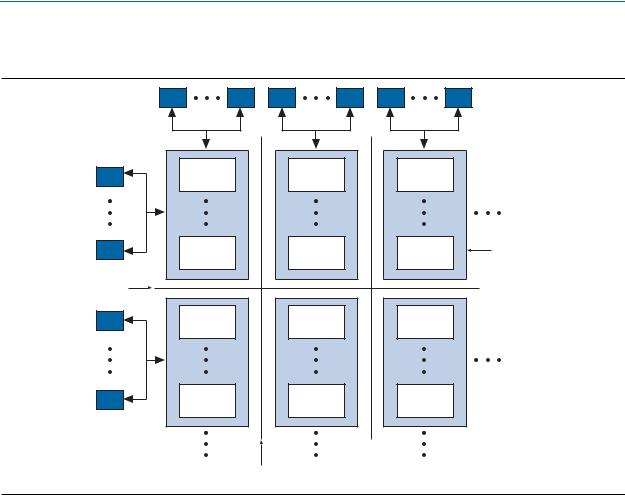
Figure 2–1 shows a functional block diagram of the MAX V device.
Figure 2–1. Device Block Diagram |
|
|
|
|
|
|
|
IOE |
|
IOE |
IOE |
IOE |
IOE |
|
IOE |
IOE |
Logic |
|
|
Logic |
|
Logic |
|
Element |
|
|
Element |
|
Element |
|
|
|
|
|
|
|
|||
IOE |
Logic |
|
|
Logic |
|
Logic |
Logic Array |
Element |
|
|
Element |
|
Element |
||
|
|
|
|
BLock (LAB) |
|||
|
|
|
|
|
|
|
|
MultiTrack |
|
|
|
|
|
|
|
Interconnect |
|
|
|
|
|
|
|
IOE |
Logic |
|
|
Logic |
|
Logic |
|
Element |
|
|
Element |
|
Element |
|
|
|
|
|
|
|
|||
IOE |
Logic |
|
|
Logic |
|
Logic |
|
Element |
|
|
Element |
|
Element |
|
|
|
|
|
|
|
|||
|
|
MultiTrack |
|
|
|
|
|
|
|
Interconnect |
|
|
|
|
|
Each MAX V device contains a flash memory block within its floorplan. This block is located on the left side of the 5M40Z, 5M80Z, 5M160Z, and 5M240Z devices. On the 5M240Z (T144 package), 5M570Z, 5M1270Z, and 5M2210Z devices, the flash memory block is located on the bottom-left area of the device. The majority of this flash memory storage is partitioned as the dedicated configuration flash memory (CFM) block. The CFM block provides the non-volatile storage for all of the SRAM configuration information. The CFM automatically downloads and configures the logic and I/O at power-up, providing instant-on operation.
fFor more information about configuration upon power-up, refer to the Hot Socketing and Power-On Reset for MAX V Devices chapter.
A portion of the flash memory within the MAX V device is partitioned into a small block for user data. This user flash memory (UFM) block provides 8,192 bits of general-purpose user storage. The UFM provides programmable port connections to the logic array for reading and writing. There are three LAB rows adjacent to this block, with column numbers varying by device.
MAX V Device Handbook |
December 2010 Altera Corporation |

Chapter 2: MAX V Architecture |
2–3 |
Functional Description
Table 2–1 lists the number of LAB rows and columns in each device, as well as the number of LAB rows and columns adjacent to the flash memory area. The long LAB rows are full LAB rows that extend from one side of row I/O blocks to the other. The short LAB rows are adjacent to the UFM block; their length is shown as width in LAB columns.
Table 2–1. Device Resources for MAX V Devices
Device |
UFM Blocks |
LAB Columns |
|
LAB Rows |
Total LABs |
|
|
|
|||||
Long LAB Rows |
Short LAB Rows (Width) (1) |
|||||
|
|
|
|
|||
|
|
|
|
|
|
|
5M40Z |
1 |
6 |
4 |
— |
24 |
|
|
|
|
|
|
|
|
5M80Z |
1 |
6 |
4 |
— |
24 |
|
|
|
|
|
|
|
|
5M160Z |
1 |
6 |
4 |
— |
24 |
|
|
|
|
|
|
|
|
5M240Z (2) |
1 |
6 |
4 |
— |
24 |
|
|
|
|
|
|
|
|
5M240Z (3) |
1 |
12 |
4 |
3 (3) |
57 |
|
|
|
|
|
|
|
|
5M570Z |
1 |
12 |
4 |
3 (3) |
57 |
|
|
|
|
|
|
|
|
5M1270Z (4) |
1 |
16 |
7 |
3 (5) |
127 |
|
|
|
|
|
|
|
|
5M1270Z (5) |
1 |
20 |
10 |
3 (7) |
221 |
|
|
|
|
|
|
|
|
5M2210Z |
1 |
20 |
10 |
3 (7) |
221 |
|
|
|
|
|
|
|
Notes to Table 2–1:
(1)The width is the number of LAB columns in length.
(2)Not applicable to T144 package of the 5M240Z device.
(3)Only applicable to T144 package of the 5M240Z device.
(4)Not applicable to F324 package of the 5M1270Z device.
(5)Only applicable to F324 package of the 5M1270Z device.
December 2010 Altera Corporation |
MAX V Device Handbook |
2–4 |
Chapter 2: MAX V Architecture |
|
Logic Array Blocks |
|
|
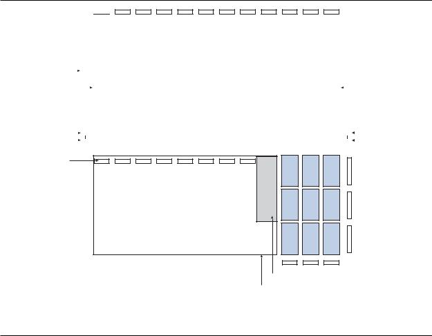
Figure 2–2 shows a floorplan of a MAX V device.
Figure 2–2. Device Floorplan for MAX V Devices (Note 1)
I/O Blocks 


I/O Blocks |
|
|
|
|
|
|
|
|
|
|
|
|
|
|
|
|
|
|
|
|
|
|
|
|
|
|
|
|
|
|
|
|
|
|
|
|
|
|
|
|
|
|
|
|
|
|
|
|
|
|
|
|
|
|
|
|
|
|
|
|
|
|
|
|
|
|
|
|
|
|
|
|
|
|
|
|
|
|
|
||
|
|
|
|
|
|
|
|
|
|
|
|
|
|
|
|
|
|
|
|
|
|
|
|
|
|
|
|
|
|
|
|
|
|
|
|
|
|
|
||
|
|
|
|
|
|
|
|
|
|
|
|
|
|
|
|
|
|
|
|
|
|
|
|
|
|
|
|
|
|
|
|
|
|
|
|
|
|
|
||
|
|
|
|
|
|
|
|
|
|
|
|
|
|
|
|
|
|
|
|
|
|
|
|
|
|
|
|
|
|
|
|
|
|
|
|
|
|
|
||
|
|
|
|
|
|
|
|
|
|
|
|
|
|
|
|
|
|
|
|
|
|
|
|
|
|
|
|
|
|
|
|
|
|
|
|
|
|
|
||
Logic Array |
|
|
|
|
|
|
|
|
|
|
|
|
|
|
|
|
|
|
|
|
|
|
|
|
|
|
|
|
|
|
|
|
|
|
|
|
|
|
Logic Array |
|
|
|
|
|
|
|
|
|
|
|
|
|
|
|
|
|
|
|
|
|
|
|
|
|
|
|
|
|
|
|
|
|
|
|
|
|
|
|
|||
Blocks |
|
|
|
|
|
|
|
|
|
|
|
|
|
|
|
|
|
|
|
|
|
|
|
|
|
|
|
|
|
|
|
|
|
|
|
|
|
|
Blocks |
|
|
|
|
|
|
|
|
|
|
|
|
|
|
|
|
|
|
|
|
|
|
|
|
|
|
|
|
|
|
|
|
|
|
|
|
|
|
|
|||
2 GCLK |
|
|
|
|
|
|
|
|
|
|
|
|
|
|
|
|
|
|
|
|
|
|
|
|
|
|
|
|
|
|
|
|
|
|
|
|
|
|
|
2 GCLK |
|
|
|
|
|
|
|
|
|
|
|
|
|
|
|
|
|
|
|
|
|
|
|
|
|
|
|
|
|
|
|
|
|
|
|
|
|
|
|
||
|
|
|
|
|
|
|
|
|
|
|
|
|
|
|
|
|
|
|
|
|
|
|
|
|
|
|
|
|
|
|
|
|
|
|
|
|
|
|
||
|
|
|
|
|
|
|
|
|
|
|
|
|
|
|
|
|
|
|
|
|
|
|
|
|
|
|
|
|
|
|
|
|
|
|
|
|
|
|
||
Inputs |
|
|
|
|
|
|
|
|
|
|
|
|
|
|
|
|
|
|
|
|
|
|
|
|
|
|
|
|
|
|
|
|
|
|
|
|
|
|
Inputs |
|
|
|
|
|
|
|
|
|
|
|
|
|
|
|
|
|
|
|
|
|
|
|
|
|
|
|
|
|
|
|
|
|
|
|
|
|
|
|
|
|
|
|
|
|
|
|
|
|
|
|
|
|
|
|
|
|
|
|
|
|
|
|
|
|
|
|
|
|
|
|
|
|
|
|
|
|
|
|
|
|
|
|
I/O Blocks
UFM Block
CFM Block
Note to Figure 2–2:
(1)The device shown is a 5M570Z device. 5M1270Z and 5M2210Z devices have a similar floorplan with more LABs. For 5M40Z, 5M80Z, 5M160Z, and 5M240Z devices, the CFM and UFM blocks are located on the left side of the device.
Logic Array Blocks
Each LAB consists of 10 LEs, LE carry chains, LAB control signals, a local interconnect, a look-up table (LUT) chain, and register chain connection lines. There are 26 possible unique inputs into an LAB, with an additional 10 local feedback input lines fed by LE outputs in the same LAB. The local interconnect transfers signals between LEs in the same LAB. LUT chain connections transfer the LUT output from one LE to the
MAX V Device Handbook |
December 2010 Altera Corporation |
Chapter 2: MAX V Architecture |
2–5 |
Logic Array Blocks
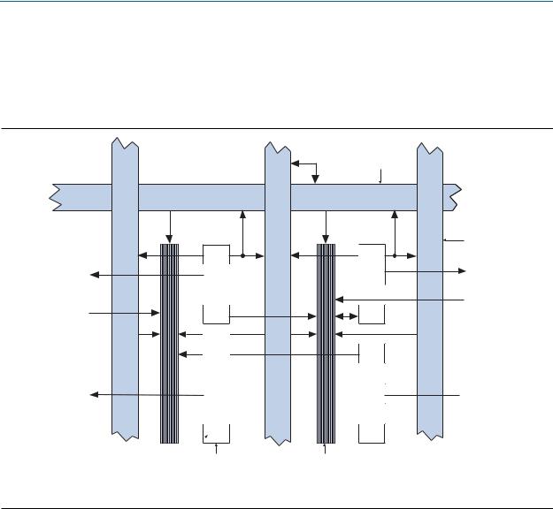
adjacent LE for fast sequential LUT connections within the same LAB. Register chain connections transfer the output of one LE’s register to the adjacent LE’s register within an LAB. The Quartus® II software places associated logic within an LAB or adjacent LABs, allowing the use of local, LUT chain, and register chain connections for performance and area efficiency. Figure 2–3 shows the MAX V LAB.
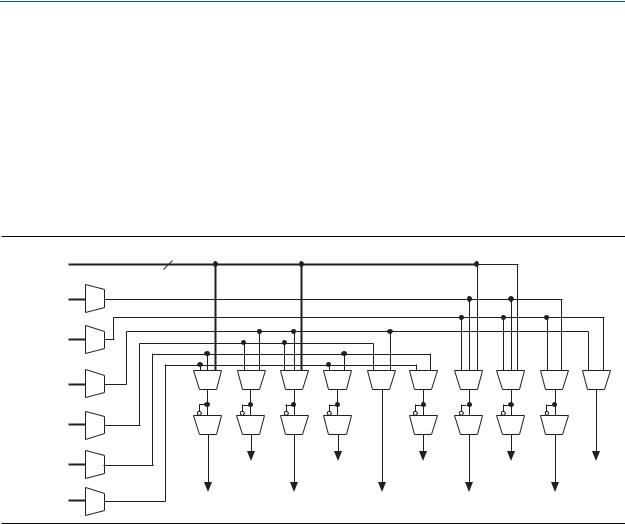
Figure 2–3. LAB Structure for MAX V Devices
Row Interconnect
Fast I/O connection to IOE (1)
DirectLink interconnect from adjacent LAB
or IOE
DirectLink interconnect to adjacent LAB or IOE
LE0
LE1
LE2

 LE3
LE3
LE4 |
LE5 |
LE6 |
LE7 |
LE8 |
LE9 |
Logic Element
LAB |
Local Interconnect |
Note to Figure 2–3:
(1) Only from LABs adjacent to IOEs.
Column Interconnect
Fast I/O connection to IOE (1)
DirectLink interconnect from adjacent LAB
or IOE
DirectLink  interconnect to adjacent LAB or IOE
December 2010 Altera Corporation |
MAX V Device Handbook |
2–6 |
Chapter 2: MAX V Architecture |
Logic Array Blocks
LAB Interconnects
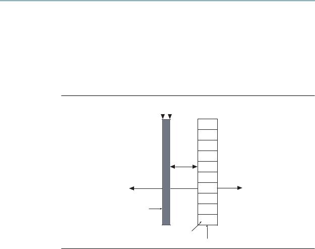
Column and row interconnects and LE outputs within the same LAB drive the LAB local interconnect. Adjacent LABs, from the left and right, can also drive an LAB’s local interconnect through the DirectLink connection. The DirectLink connection feature minimizes the use of row and column interconnects, providing higher performance and flexibility. Each LE can drive 30 other LEs through fast local and DirectLink interconnects. Figure 2–4 shows the DirectLink connection.
Figure 2–4. DirectLink Connection
DirectLink interconnect from |
|
|
|
DirectLink interconnect from |
left LAB or IOE output |
|
|
right LAB or IOE output |
|
|
|
|
|
|
|
LE0 |
|
|
|
LE1 |
|
|
|
LE2 |
|
|
|
LE3 |
|
|
|
LE4 |
|
|
DirectLink |
LE5 |
DirectLink |
|
LE6 |
|||
interconnect |
interconnect |
||
to left |
LE7 |
to right |
|
|
|
||
Local |
LE8 |
|
|
Interconnect |
|
||
|
|
||
|
LE9 |
|
|
|
Logic Element |
|
|
|
LAB |
|
LAB Control Signals
Each LAB contains dedicated logic for driving control signals to its LEs. The control signals include two clocks, two clock enables, two asynchronous clears, a synchronous clear, an asynchronous preset/load, a synchronous load, and add/subtract control signals, providing a maximum of 10 control signals at a time. Synchronous load and clear signals are generally used when implementing counters but they can also be used with other functions.
Each LAB can use two clocks and two clock enable signals. Each LAB’s clock and clock enable signals are linked. For example, any LE in a particular LAB using the labclk1 signal also uses labclkena1. If the LAB uses both the rising and falling edges of a clock, it also uses both LAB-wide clock signals. Deasserting the clock enable signal turns off the LAB-wide clock.
Each LAB can use two asynchronous clear signals and an asynchronous load/preset signal. By default, the Quartus II software uses a NOT gate push-back technique to achieve preset. If you disable the NOT gate push-back option or assign a given register to power-up high using the Quartus II software, the preset is then achieved using the asynchronous load signal with asynchronous load data input tied high.
MAX V Device Handbook |
December 2010 Altera Corporation |
Chapter 2: MAX V Architecture |
2–7 |
Logic Array Blocks
With the LAB-wide addnsub control signal, a single LE can implement a one-bit adder and subtractor. This signal saves LE resources and improves performance for logic functions such as correlators and signed multipliers that alternate between addition and subtraction depending on data.
The LAB column clocks [3..0], driven by the global clock network, and LAB local interconnect generate the LAB-wide control signals. The MultiTrack interconnect structure drives the LAB local interconnect for non-global control signal generation. The MultiTrack interconnect’s inherent low skew allows clock and control signal distribution in addition to data signals. Figure 2–5 shows the LAB control signal generation circuit.
Figure 2–5. LAB-Wide Control Signals |
|
|
|
|
|
|
Dedicated |
4 |
|
|
|
|
|
LAB Column |
|
|
|
|
|
|
|
|
|
|
|
|
|
Clocks |
|
|
|
|
|
|
Local |
|
|
|
|
|
|
Interconnect |
|
|
|
|
|
|
Local |
|
|
|
|
|
|
Interconnect |
|
|
|
|
|
|
Local |
|
|
|
|
|
|
Interconnect |
|
|
|
|
|
|
Local |
|
|
|
|
|
|
Interconnect |
|
|
|
|
|
|
Local |
|
labclkena1 |
labclkena2 |
syncload |
labclr2 |
addnsub |
Interconnect |
|
|||||
Local |
labclk1 |
labclk2 |
asyncload |
labclr1 |
|
synclr |
Interconnect |
|
|||||
|
|
or labpre |
|
|
|
|
|
|
|
|
|
|
|
December 2010 Altera Corporation |
MAX V Device Handbook |
2–8 |
Chapter 2: MAX V Architecture |
Logic Elements
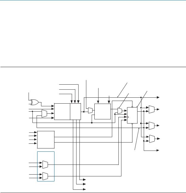
Logic Elements
The smallest unit of logic in the MAX V architecture, the LE, is compact and provides advanced features with efficient logic utilization. Each LE contains a four-input LUT, which is a function generator that can implement any function of four variables. In addition, each LE contains a programmable register and carry chain with carry-select capability. A single LE also supports dynamic single-bit addition or subtraction mode that is selected by an LAB-wide control signal. Each LE drives all types of interconnects: local, row, column, LUT chain, register chain, and DirectLink interconnects as shown in Figure 2–6.
Figure 2–6. LE for MAX V Devices
Register chain routing from previous LE
|
|
|
LAB-wide |
Register Bypass |
|
|
|
LAB Carry-In |
|
Synchronous |
|
|
|
|
|
Load |
|
|
Programmable |
|
|
|
|
Packed |
|
||
addnsub |
Carry-In1 |
|
LAB-wide |
|
Register |
|
|
Synchronous |
Register Select |
||||
Carry-In0 |
|
|
||||
|
|
Clear |
|
|
LUT chain |
|
|
|
|
|
|
|
|
|
|
|
|
|
|
routing to next LE |
data1 |
|
|
|
|
|
Row, column, |
data2 |
Look-Up |
|
Synchronous |
|
|
|
Carry |
PRN/ALD |
and DirectLink |
||||
data3 |
Table |
Load and |
D |
Q |
routing |
|
Chain |
ADATA |
|
||||
|
(LUT) |
Clear Logic |
|
|
||
data4 |
|
|
|
|||
|
|
|
ENA |
|
|
|
|
|
|
|
|
|
|
|
|
|
|
CLRN |
|
Row, column, |
|
|
|
|
|
|
and DirectLink |
|
|
|
|
|
|
routing |
labclr1 |
|
|
|
|
|
|
labclr2 |
Asynchronous |
|
|
|
|
Local routing |
labpre/aload |
Clear/Preset/ |
|
|
|
|
|
Chip-Wide |
Load Logic |
|
|
|
|
|
Reset (DEV_CLRn) |
|
|
|
|
|
|
|
|
|
|
Register |
Register chain |
|
|
Clock and |
|
|
output |
||
|
|
|
Feedback |
|
||
|
Clock Enable |
|
|
|
||
|
|
|
|
|
|
|
|
Select |
|
|
|
|
|
labclk1 |
|
|
|
|
|
|
labclk2 |
|
|
|
|
|
|
labclkena1 |
|
|
|
|
|
|
labclkena2 |
|
|
Carry-Out0 |
|
|
|
|
|
|
|
|
|
|
|
|
|
Carry-Out1 |
|
|
|
|
|
|
LAB Carry-Out |
|
|
|
You can configure each LE’s programmable register for D, T, JK, or SR operation. Each register has data, true asynchronous load data, clock, clock enable, clear, and asynchronous load/preset inputs. Global signals, general purpose I/O (GPIO) pins, or any LE can drive the register’s clock and clear control signals. Either GPIO pins or LEs can drive the clock enable, preset, asynchronous load, and asynchronous data. The asynchronous load data input comes from the data3 input of the LE. For combinational functions, the LUT output bypasses the register and drives directly to the LE outputs.
Each LE has three outputs that drive the local, row, and column routing resources. The LUT or register output can drive these three outputs independently. Two LE outputs drive either a column or row and DirectLink routing connections while one output drives the local interconnect resources. This configuration allows the LUT to drive one output while the register drives another output. This register packing feature
MAX V Device Handbook |
December 2010 Altera Corporation |
Chapter 2: MAX V Architecture |
2–9 |
Logic Elements |
|
|
|
improves device utilization because the device can use the register and the LUT for unrelated functions. Another special packing mode allows the register output to feed back into the LUT of the same LE so that the register is packed with its own fan-out LUT. This mode provides another mechanism for improved fitting. The LE can also drive out registered and unregistered versions of the LUT output.
LUT Chain and Register Chain
In addition to the three general routing outputs, the LEs within a LAB have LUT chain and register chain outputs. LUT chain connections allow LUTs within the same LAB to cascade together for wide input functions. Register chain outputs allow registers within the same LAB to cascade together. The register chain output allows a LAB to use LUTs for a single combinational function and the registers for an unrelated shift register implementation. These resources speed up connections between LABs while saving local interconnect resources. For more information about LUT chain and register chain connections, refer to “MultiTrack Interconnect” on page 2–14.
addnsub Signal
The LE’s dynamic adder/subtractor feature saves logic resources by using one set of LEs to implement both an adder and a subtractor. This feature is controlled by the LAB-wide control signal addnsub. The addnsub signal sets the LAB to perform either A + B or A – B. The LUT computes addition; subtraction is computed by adding the two’s complement of the intended subtractor. The LAB-wide signal converts to two’s complement by inverting the B bits within the LAB and setting carry-in to 1, which adds one to the LSB. The LSB of an adder/subtractor must be placed in the first LE of the LAB, where the LAB-wide addnsub signal automatically sets the carry-in to 1. The Quartus II Compiler automatically places and uses the adder/subtractor feature when using adder/subtractor parameterized functions.
LE Operating Modes
The MAX V LE can operate in one of the following modes:
■“Normal Mode”
■“Dynamic Arithmetic Mode”
Each mode uses LE resources differently. In each mode, eight available inputs to the LE, the four data inputs from the LAB local interconnect, carry-in0 and carry-in1 from the previous LE, the LAB carry-in from the previous carry-chain LAB, and the register chain connection are directed to different destinations to implement the desired logic function. LAB-wide signals provide clock, asynchronous clear, asynchronous preset/load, synchronous clear, synchronous load, and clock enable control for the register. These LAB-wide signals are available in all LE modes. The addnsub control signal is allowed in arithmetic mode.
The Quartus II software, along with parameterized functions such as the library of parameterized modules (LPM) functions, automatically chooses the appropriate mode for common functions such as counters, adders, subtractors, and arithmetic functions.
December 2010 Altera Corporation |
MAX V Device Handbook |
2–10 |
Chapter 2: MAX V Architecture |
Logic Elements
Normal Mode
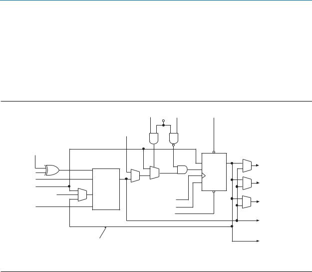
The normal mode is suitable for general logic applications and combinational functions. In normal mode, four data inputs from the LAB local interconnect are inputs to a four-input LUT as shown in Figure 2–7. The Quartus II Compiler automatically selects the carry-in or the data3 signal as one of the inputs to the LUT. Each LE can use LUT chain connections to drive its combinational output directly to the next LE in the LAB. Asynchronous load data for the register comes from the data3 input of the LE. LEs in normal mode support packed registers.
Figure 2–7. LE in Normal Mode
sload |
sclear |
aload |
(LAB Wide) |
(LAB Wide) |
(LAB Wide) |
|
Register chain |
|
|
|
|
connection |
|
|
|
addnsub (LAB Wide) |
|
|
|
|
(1) |
|
ALD/PRE |
|
|
|
ADATA Q |
Row, column, and |
||
|
|
|||
data1 |
|
D |
DirectLink routing |
|
|
|
|
||
data2 |
|
ENA |
Row, column, and |
|
data3 |
4-Input |
DirectLink routing |
||
CLRN |
||||
|
||||
cin (from cout |
LUT |
|
|
|
of previous LE) |
clock (LAB Wide) |
|
Local routing |
|
|
|
|||
data4 |
|
|
||
ena (LAB Wide) |
|
|
||
|
aclr (LAB Wide) |
|
LUT chain |
|
|
|
|
||
|
|
|
connection |
|
|
Register Feedback |
|
Register |
|
|
|
chain output |
||
|
|
|
Note to Figure 2–7:
(1) This signal is only allowed in normal mode if the LE is after an adder/subtractor chain.
Dynamic Arithmetic Mode
The dynamic arithmetic mode is ideal for implementing adders, counters, accumulators, wide parity functions, and comparators. A LE in dynamic arithmetic mode uses four 2-input LUTs configurable as a dynamic adder/subtractor. The first two 2-input LUTs compute two summations based on a possible carry-in of 1 or 0; the other two LUTs generate carry outputs for the two chains of the carry-select circuitry. As shown in Figure 2–8, the LAB carry-in signal selects either the carry-in0 or carry-in1 chain. The selected chain’s logic level in turn determines which parallel sum is generated as a combinational or registered output. For example, when implementing an adder, the sum output is the selection of two possible calculated sums:
data1 + data2 + carry-in0
or
data1 + data2 + carry-in1
MAX V Device Handbook |
December 2010 Altera Corporation |
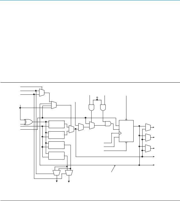
Chapter 2: MAX V Architecture |
2–11 |
Logic Elements
The other two LUTs use the data1 and data2 signals to generate two possible carry-out signals: one for a carry of 1 and the other for a carry of 0. The carry-in0 signal acts as the carry-select for the carry-out0 output and carry-in1 acts as the carry-select for the carry-out1 output. LEs in arithmetic mode can drive out registered and unregistered versions of the LUT output.
The dynamic arithmetic mode also offers clock enable, counter enable, synchronous up/down control, synchronous clear, synchronous load, and dynamic adder/subtractor options. The LAB local interconnect data inputs generate the counter enable and synchronous up/down control signals. The synchronous clear and synchronous load options are LAB-wide signals that affect all registers in the LAB. The Quartus II software automatically places any registers that are not used by the counter into other LABs. The addnsub LAB-wide signal controls whether the LE acts as an adder or subtractor.
Figure 2–8. LE in Dynamic Arithmetic Mode
LAB Carry-In
Carry-In0 |
|
sload |
sclear |
aload |
|
Carry-In1 |
|
(LAB Wide) |
(LAB Wide) |
(LAB Wide) |
|
|
Register chain |
|
|
|
|
addnsub |
|
|
|
|
|
|
connection |
|
|
|
|
(LAB Wide) |
|
|
|
|
|
|
|
|
|
|
|
(1) |
|
|
|
|
|
data1 |
LUT |
|
|
ALD/PRE |
|
data2 |
|
|
ADATA Q |
Row, column, and |
|
|
|
|
|||
data3 |
|
|
|
D |
direct link routing |
|
LUT |
|
|
ENA |
Row, column, and |
|
|
|
|
direct link routing |
|
|
|
|
|
CLRN |
|
|
|
|
|
|
|
|
LUT |
clock (LAB Wide) |
|
|
|
|
ena (LAB Wide) |
|
|
||
|
|
|
Local routing |
||
|
|
aclr (LAB Wide) |
|
||
|
|
|
|
||
|
LUT |
|
|
|
LUT chain |
|
|
|
|
|
connection |
|
|
|
|
|
Register |
|
|
|
|
|
chain output |
|
|
|
Register Feedback |
|
|
|
Carry-Out0 |
Carry-Out1 |
|
|
|
Note to Figure 2–8:
(1) The addnsub signal is tied to the carry input for the first LE of a carry chain only.
Carry-Select Chain
The carry-select chain provides a very fast carry-select function between LEs in dynamic arithmetic mode. The carry-select chain uses the redundant carry calculation to increase the speed of carry functions. The LE is configured to calculate outputs for a possible carry-in of 0 and carry-in of 1 in parallel. The carry-in0 and carry-in1 signals from a lower-order bit feed forward into the higher-order bit via the parallel carry chain and feed into both the LUT and the next portion of the carry chain. Carry-select chains can begin in any LE within an LAB.
December 2010 Altera Corporation |
MAX V Device Handbook |
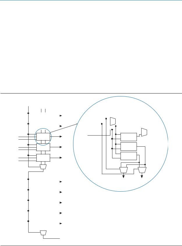
2–12 |
Chapter 2: MAX V Architecture |
Logic Elements
The speed advantage of the carry-select chain is in the parallel pre-computation of carry chains. Because the LAB carry-in selects the precomputed carry chain, not every LE is in the critical path. Only the propagation delays between LAB carry-in generation (LE5 and LE10) are now part of the critical path. This feature allows the MAX V architecture to implement high-speed counters, adders, multipliers, parity functions, and comparators of arbitrary width.
Figure 2–9 shows the carry-select circuitry in an LAB for a 10-bit full adder. One portion of the LUT generates the sum of two bits using the input signals and the appropriate carry-in bit; the sum is routed to the output of the LE. The register can be bypassed for simple adders or used for accumulator functions. Another portion of the LUT generates carry-out bits. An LAB-wide carry-in bit selects which chain is used for the addition of given inputs. The carry-in signal for each chain, carry-in0 or carry-in1, selects the carry-out to carry forward to the carry-in signal of the next-higher-order bit. The final carry-out signal is routed to an LE, where it is fed to local, row, or column interconnects.
Figure 2–9. Carry-Select Chain
LAB Carry-In |
1 |
0 |
|
|
|
|
|
Sum1 |
LAB Carry-In |
|
|
|
|
|
|
|
|
|||
A1 |
|
|
LE0 |
Carry-In0 |
|
|
|
|
|
|
|
|
|||||
B1 |
|
|
|
|
|
|
|
|
|
|
|
||||||
|
|
|
|
|
|
|
|
|
|
|
|
|
|||||
A2 |
|
|
|
|
Sum2 |
Carry-In1 |
|
|
|
|
|
|
|
|
|||
|
|
|
|
|
|
|
|
|
|
|
|
||||||
|
|
LE1 |
|
|
|
|
|
|
LUT |
|
|
|
|
||||
B2 |
|
|
|
data1 |
|
|
|
|
|
|
|
|
|
||||
|
|
|
|
|
|
|
|
|
|
|
|
||||||
|
|
|
|
|
|
|
|
|
|
|
|
|
|
|
|||
|
|
|
|
|
|
|
|
|
|
|
|
|
|
|
|
Sum |
|
|
|
|
|
|
|
|
|
|
|
|
|
|
|
|
|||
|
|
|
|
|
|
|
|
|
|
|
|
|
|
|
|
||
|
|
|
|
|
|
|
|
|
|
|
|
|
|
|
|
|
|
A3 |
|
Sum3 |
data2 |
|
LE2 |
LUT |
|||
|
||||
B3 |
|
|
|
|
A4 |
LE3 |
Sum4 |
LUT |
|
B4 |
|
|
|
|
A5 |
LE4 |
Sum5 |
LUT |
|
B5 |
|
|
||
|
|
|
0 1
|
|
|
|
|
Sum6 |
Carry-Out0 |
Carry-Out1 |
A6 |
|
|
LE5 |
||||
B6 |
|
|
|
|
|||
|
|
|
|
|
|
||
|
|
|
|
|
Sum7 |
|
|
|
|
|
|
|
|
|
|
A7 |
|
|
LE6 |
|
|
||
B7 |
|
|
|
|
|||
|
|
|
|
|
|
||
|
|
|
|
|
Sum8 |
|
|
|
|
|
|
|
|
|
|
A8 |
|
LE7 |
|
|
|||
B8 |
|
|
|
|
|||
|
|
|
|
|
|
||
|
|
|
|
|
Sum9 |
|
|
|
|
|
|
|
|
|
|
A9 |
|
|
LE8 |
|
|
||
B9 |
|
|
|
|
|||
|
|
|
|
|
|
||
|
|
|
|
|
Sum10 |
|
|
|
|
|
|
|
|
|
|
A10 |
|
LE9 |
|
|
|||
B10 |
|
|
|
|
|||
|
|
|
|
|
|
||
|
|
|
|
|
|
|
|
|
|
|
|
|
|
|
|
 To top of adjacent LAB
LAB Carry-Out
MAX V Device Handbook |
December 2010 Altera Corporation |
Chapter 2: MAX V Architecture |
2–13 |
Logic Elements |
|
|
|
The Quartus II software automatically creates carry chain logic during design processing, or you can create it manually during design entry. Parameterized functions such as LPM functions automatically take advantage of carry chains for the appropriate functions. The Quartus II software creates carry chains longer than 10 LEs by linking adjacent LABs within the same row together automatically. A carry chain can extend horizontally up to one full LAB row, but does not extend between LAB rows.
Clear and Preset Logic Control
LAB-wide signals control the logic for the register’s clear and preset signals. The LE directly supports an asynchronous clear and preset function. The register preset is achieved through the asynchronous load of a logic high. MAX V devices support simultaneous preset/asynchronous load and clear signals. An asynchronous clear signal takes precedence if both signals are asserted simultaneously. Each LAB supports up to two clears and one preset signal.
In addition to the clear and preset ports, MAX V devices provide a chip-wide reset pin (DEV_CLRn) that resets all registers in the device. An option set before compilation in the Quartus II software controls this pin. This chip-wide reset overrides all other control signals and uses its own dedicated routing resources without using any of the four global resources. Driving this signal low before or during power-up prevents user mode from releasing clears within the design. This allows you to control when clear is released on a device that has just been powered-up. If not set for its chip-wide reset function, the DEV_CLRn pin is a regular I/O pin.
By default, all registers in MAX V devices are set to power-up low. However, this power-up state can be set to high on individual registers during design entry using the Quartus II software.
LE RAM
The Quartus II memory compiler can configure the unused LEs as LE RAM.
MAX V devices support the following memory types:
■FIFO synchronous R/W
■FIFO asynchronous R/W
■1 port SRAM
■2 port SRAM
■3 port SRAM
■shift registers
fFor more information about memory, refer to the Internal Memory (RAM and ROM) User Guide.
December 2010 Altera Corporation |
MAX V Device Handbook |
2–14 |
Chapter 2: MAX V Architecture |
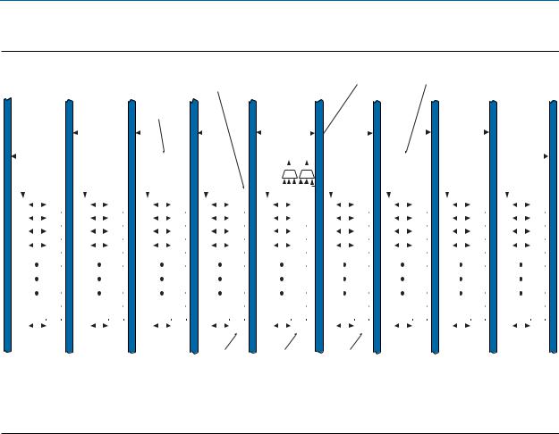
Chapter 2: MAX V Architecture |
2–15 |
MultiTrack Interconnect
Figure 2–10. R4 Interconnect Connections
Adjacent LAB can drive onto another LAB’s R4 Interconnect
R4 Interconnect
Driving Left
|
|
|
|
|
|
C4 Column Interconnects (1) |
R4 Interconnect |
|
|
|
|
|
|||||||||||||||||||||||||||||||||
|
|
|
|
|
|
Driving Right |
|
|
|
|
|
||||||||||||||||||||||||||||||||||
|
|
|
|
|
|
|
|
|
|
|
|
|
|
|
|
|
|
|
|
|
|
|
|
|
|
|
|
|
|
|
|
|
|
|
|
|
|
|
|
|
|
|
|
|
|
|
|
|
|
|
|
|
|
|
|
|
|
|
|
|
|
|
|
|
|
|
|
|
|
|
|
|
|
|
|
|
|
|
|
|
|
|
|
|
|
|
|
|
|
|
|
|
|
|
|
|
|
|
|
|
|
|
|
|
|
|
|
|
|
|
|
|
|
|
|
|
|
|
|
|
|
|
|
|
|
|
|
|
|
|
|
|
|
|
|
|
|
|
|
|
|
|
|
|
|
|
|
|
|
|
|
|
|
|
|
|
|
|
|
|
|
|
|
|
|
|
|
|
|
|
|
|
|
|
|
|
|
|
|
|
|
|
|
|
|
|
|
|
|
|
|
|
|
|
|
|
|
|
|
|
|
|
|
|
|
|
|
|
|
|
|
|
|
|
|
|
|
|
|
|
|
|
|
|
|
|
|
|
|
|
|
|
|
|
|
|
|
|
|
|
|
|
|
|
|
|
|
|
|
|
|
|
|
|
|
|
|
|
|
|
|
|
|
|
|
|
|
|
|
|
|
|
|
|
|
|
|
|
|
|
|
|
|
|
|
|
|
|
|
|
|
|
|
|
|
|
|
|
|
|
|
|
|
|
|
|
|
|
|
|
|
|
|
|
|
|
|
|
|
|
|
|
|
|
|
|
|
|
|
|
|
|
|
|
|
|
|
|
|
|
|
|
|
|
|
|
|
|
|
|
|
|
|
|
|
|
|
|
|
|
|
|
|
|
|
|
|
|
|
|
|
|
|
|
|
|
|
|
|
|
|
|
|
|
|
|
|
|
|
|
|
|
|
|
|
|
|
|
|
|
|
|
|
|
|
|
|
|
|
|
|
|
|
|
|
|
|
|
|
|
|
|
|
|
|
|
|
|
|
|
|
|
|
|
|
|
|
|
|
|
|
|
|
|
|
|
|
|
|
|
|
|
|
|
|
|
|
|
|
|
|
|
|
|
|
|
|
|
|
|
|
|
|
|
|
|
|
|
|
|
|
|
|
|
|
|
|
|
|
|
|
|
|
|
|
|
|
|
|
|
|
|
|
|
|
|
|
|
|
|
|
|
|
|
|
|
|
|
|
|
|
|
|
|
|
|
|
|
|
|
|
|
|
|
|
|
|
|
|
|
|
|
|
|
|
|
|
|
|
|
|
|
|
|
|
|
|
|
|
|
|
|
|
|
|
|
|
|
|
|
|
|
|
|
|
|
|
|
|
|
|
|
|
|
|
|
|
|
|
|
|
|
|
|
|
|
|
|
|
|
|
|
|
|
|
|
|
|
|
|
|
|
|
|
|
|
|
|
|
|
|
|
|
|
|
|
|
|
|
|
|
|
|
|
|
|
|
|
|
|
|
|
|
|
|
|
|
|
|
|
|
|
|
|
|
|
|
|
|
|
|
|
|
|
|
|
|
|
|
|
|
|
|
|
|
|
|
|
|
|
|
|
|
|
|
|
|
|
|
|
|
|
|
|
|
|
|
|
|
|
|
|
|
|
|
|
|
|
|
|
|
|
|
|
|
|
|
|
|
|
|
|
|
|
|
|
|
|
|
|
|
|
|
|
|
|
|
|
|
|
|
|
|
|
|
|
|
|
|
|
|
|
|
|
|
|
|
|
|
|
|
|
|
|
|
|
|
|
|
|
|
|
|
|
|
|
|
|
|
|
|
|
|
|
|
|
|
|
|
|
|
|
|
|
|
|
|
|
|
|
|
|
|
|
|
|
|
|
|
|
|
|
|
|
|
|
|
|
|
|
|
|
|
|
|
|
|
|
|
|
|
|
|
|
|
|
|
|
|
|
|
|
|
|
|
|
|
|
|
|
|
|
|
|
|
|
|
|
|
|
|
|
|
|
|
|
|
|
|
|
|
|
|
|
|
|
|
|
|
|
|
|
|
|
|
|
|
|
|
|
|
|
|
|
|
|
|
|
|
|
|
|
|
|
|
|
|
|
|
|
|
|
|
|
|
|
|
|
|
|
|
|
|
|
|
|
|
|
|
|
|
|
|
|
|
|
|
|
|
|
|
|
|
|
|
|
|
|
|
|
|
|
|
|
|
|
|
|
|
|
|
|
|
|
|
|
|
|
|
|
|
|
|
|
|
|
|
|
|
|
|
|
|
|
|
|
|
|
|
|
|
|
|
|
|
|
|
|
|
|
|
|
|
|
|
|
|
|
|
|
|
|
|
|
|
|
|
|
|
|
|
|
|
|
|
|
|
|
|
|
|
|
|
|
|
|
|
|
|
|
|
|
|
|
|
|
|
|
|
|
|
|
|
|
|
|
|
|
|
|
|
|
|
|
|
|
|
|
|
|
|
|
|
|
|
|
|
|
|
|
|
|
|
|
|
|
|
|
|
|
|
|
|
|
|
|
|
|
|
|
|
|
|
|
|
|
|
|
|
|
|
|
|
|
|
|
|
|
|
|
|
|
|
|
|
|
|
|
|
|
|
|
|
|
|
|
|
|
|
|
|
|
|
|
|
|
|
|
|
|
|
|
|
|
|
|
|
|
|
|
|
|
|
|
|
|
|
|
|
|
|
|
|
|
|
|
|
|
|
|
|
|
|
|
Primary |
||
|
|
|
|
|
|
|
|
|
|
|
|
|
|
|
|
|
|
|
|
|
|
|
|
|
|
|
|
|
|
|
|
|
|
|||
|
|
|
|
|
|
|
|
|
|
|
|
|
|
|
|
|
|
|
|
|
|
|
|
|
|
|
|
|
|
|
|
|
|
|||
|
|
|
|
|
|
|
|
|
|
|
|
|
|
|
|
|
|
|
|
|
|
|
|
|
|
|
|
|
|
|
|
|
|
|||
|
|
|
|
|
|
|
|
|
|
|
|
|
|
|
|
|
|
|
|
|
|
|
|
|
|
|
|
|
|
|
|
|
|
|||
|
|
|
|
|
|
|
|
|
|
|
|
|
|
|
|
|
|
|
|
|
|
|
|
|
|
|
|
|
|
|
|
|
|
|||
|
|
|
|
|
|
|
|
|
|
|
|
|
|
|
|
|
|
|
|
|
|
|
|
|
|
|
|
|
|
|
|
|
|
|||
|
|
|
|
|
|
|
|
|
|
|
|
|
|
|
|
|
|
|
|
|
|
|
|
|
|
|
|
|
|
|
|
|
|
|||
|
|
|
|
|
|
|
|
|
|
|
|
|
|
|
|
|
|
|
|
|
|
|
|
|
|
|
|
|
|
|
|
|
|
|||
|
|
|
|
|
|
|
|
|
|
|
|
|
|
|
|
|
|
|
|
|
|
|
|
|
|
|
|
|
|
|
|
|
|
|||
|
|
|
|
|
|
|
|
|
|
|
|
|
|
|
|
|
|
|
|
|
|
|
|
|
|
|
|
|
|
|
|
|
|
|||
|
|
|
|
|
|
|
|
|
|
|
|
|
|
|
|
|
|
|
|
|
|
|
|
|
|
|
|
|
|
|
|
|
|
|||
|
|
|
|
|
|
|
|
|
|
|
|
|
|
|
|
|
|
|
|
|
|
|
|
|
|
|
|
|
|
|
|
|
|
|||
|
|
|
|
|
|
|
|
|
|
|
|
|
|
|
|
|
|
|
|
|
|
|
|
|
|
|
|
|
|
|
|
|
|
|||
|
|
|
|
|
|
|
|
|
|
|
|
|
|
|
|
|
|
|
|
|
|
|
|
|
|
|
|
|
|
|
|
|
|
|||
|
|
|
|
|
|
|
|
|
|
|
|
|
|
|
|
|
|
|
|
|
|
|
|
|
|
|
|
|
|
|
|
|
|
|||
|
|
|
|
|
|
|
|
|
|
|
|
|
|
|
|
|
|
|
|
|
|
|
|
|
LAB |
|
|
|
||||||||
|
|
|
|
|
|
|
|
|
|
|
|
|
|
|
|
|
|
|
|
|
|
|
|
|
Neighbor |
|
|
|
LAB (2) |
|||||||
LAB
Neighbor
Notes to Figure 2–10:
(1)C4 interconnects can drive R4 interconnects.
(2)This pattern is repeated for every LAB in the LAB row.
The column interconnect operates similarly to the row interconnect. Each column of LABs is served by a dedicated column interconnect, which vertically routes signals to and from LABs and row and column IOEs. These column resources include:
■LUT chain interconnects within an LAB
■Register chain interconnects within an LAB
■C4 interconnects traversing a distance of four LABs in an up and down direction
MAX V devices include an enhanced interconnect structure within LABs for routing LE output to LE input connections faster using LUT chain connections and register chain connections. The LUT chain connection allows the combinational output of an LE to directly drive the fast input of the LE right below it, bypassing the local interconnect. These resources can be used as a high-speed connection for wide fan-in functions from LE 1 to LE 10 in the same LAB. The register chain connection allows the register output of one LE to connect directly to the register input of the next LE in the LAB for fast shift registers. The Quartus II Compiler automatically takes advantage of these resources to improve utilization and performance. Figure 2–11 shows the LUT chain and register chain interconnects.
December 2010 Altera Corporation |
MAX V Device Handbook |
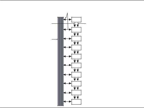
2–16 |
Chapter 2: MAX V Architecture |
|
MultiTrack Interconnect |
|
|
Figure 2–11. LUT Chain and Register Chain Interconnects
Local Interconnect
Routing Among LEs
in the LAB
LUT Chain |
LE0 |
|
Routing to |
|
|
Adjacent LE |
|
|
|
LE1 |
|
Local |
LE2 |
|
Interconnect |
||
|
||
|
LE3 |
|
|
LE4 |
|
|
LE5 |
|
|
LE6 |
|
|
LE7 |
|
|
LE8 |
|
|
LE9 |
Register Chain Routing to Adjacent LE's Register Input
The C4 interconnects span four LABs up or down from a source LAB. Every LAB has its own set of C4 interconnects to drive either up or down. Figure 2–12 shows the C4 interconnect connections from an LAB in a column. The C4 interconnects can drive and be driven by column and row IOEs. For LAB interconnection, a primary LAB or its vertical LAB neighbor can drive a given C4 interconnect. C4 interconnects can drive each other to extend their range as well as drive row interconnects for column-to-column connections.
MAX V Device Handbook |
December 2010 Altera Corporation |

Chapter 2: MAX V Architecture |
2–17 |
MultiTrack Interconnect
Figure 2–12. C4 Interconnect Connections (Note 1)
Row
Interconnect
Adjacent LAB can  drive onto neighboring

 LAB's C4 interconnect
Local
Interconnect
C4 Interconnect
Drives Local and R4
Interconnects
Up to Four Rows
C4 Interconnect
Driving Up
LAB
C4 Interconnect
Driving Down
Note to Figure 2–12:
(1) Each C4 interconnect can drive either up or down four rows.
December 2010 Altera Corporation |
MAX V Device Handbook |
2–18 |
Chapter 2: MAX V Architecture |
|
MultiTrack Interconnect |
|
|
The UFM block communicates with the logic array similar to LAB-to-LAB interfaces. The UFM block connects to row and column interconnects and has local interconnect regions driven by row and column interconnects. This block also has DirectLink interconnects for fast connections to and from a neighboring LAB. For more information about the UFM interface to the logic array, refer too “User Flash Memory Block” on page 2–21.
Table 2–2 lists the MAX V device routing scheme.
Table 2–2. Routing Scheme for MAX V Devices
|
|
|
|
|
Destination |
|
|
|
|
|
||
Source |
|
|
|
|
|
|
|
|
|
|
|
|
LUT |
Register |
Local |
DirectLink |
R4 (1) |
C4 (1) |
LE |
UFM |
Column |
Row |
Fast I/O |
||
|
||||||||||||
|
Chain |
Chain |
(1) |
(1) |
Block |
IOE |
IOE |
(1) |
||||
|
|
|
|
|||||||||
|
|
|
|
|
|
|
|
|
|
|
|
|
LUT Chain |
— |
— |
— |
— |
— |
— |
v |
— |
— |
— |
— |
|
Register Chain |
— |
— |
— |
— |
— |
— |
v |
— |
— |
— |
— |
|
Local |
— |
— |
— |
— |
— |
— |
v |
v |
v |
v |
— |
|
Interconnect |
||||||||||||
|
|
|
|
|
|
|
|
|
|
|
|
|
DirectLink |
— |
— |
v |
— |
— |
— |
— |
— |
— |
— |
— |
|
Interconnect |
||||||||||||
|
|
|
|
|
|
|
|
|
|
|
|
|
R4 Interconnect |
— |
— |
v |
— |
v |
v |
— |
— |
— |
— |
— |
|
C4 Interconnect |
— |
— |
v |
— |
v |
v |
— |
— |
— |
— |
— |
|
LE |
v |
v |
v |
v |
v |
v |
— |
— |
v |
v |
v |
|
UFM Block |
— |
— |
v |
v |
v |
v |
— |
— |
— |
— |
— |
|
Column IOE |
— |
— |
— |
— |
— |
v |
— |
— |
— |
— |
— |
|
Row IOE |
— |
— |
— |
v |
v |
v |
— |
— |
— |
— |
— |
|
Note to Table 2–2:
(1) These categories are interconnects.
MAX V Device Handbook |
December 2010 Altera Corporation |
Loading...