


 Loading...
ALTPLL (Phase-Locked Loop) IP Core User Guide
2014.08.18
ug-altpll |
Subscribe |
Send Feedback |
The Altera Phase-Locked Loop (ALTPLL) IP core implements phase lock loop (PLL) circuitry. A PLL is a feedback control system that automatically adjusts the phase of a locally generated signal to match the phase of an input signal. PLLs operate by producing an oscillator frequency to match the frequency of an input signal. In this locked condition, any slight change in the input signal first appears as a change in phase between the input signal and the oscillator frequency.
This phase shift then acts as an error signal to change the frequency of the local PLL oscillator to match the input signal. The locking-onto-a-phase relationship between the input signal and the local oscillator accounts for the name phase-locked loop. PLLs are often used in high-speed communication applications
You can use the Quartus® II IP Catalog and parameter editor to specify PLL parameters .
Note: This IP core is not supported for Arria 10 designs.
Related Information
•Introduction to Altera IP Cores
•Altera IP Release Notes
ALTPLL Features
The PLL types, operation modes, and advanced features are available for configuration in the ALTPLL IP core. Each PLL feature includes a table that compares the PLL feature in the supported devices, and describes the relevant parameter settings.
Phase-Locked Loop
The Phase-Locked Loop (PLL) is a closed-loop frequency-control system that compares the phase difference between the input signal and the output signal of a voltage-controlled oscillator (VCO). The negative feedback loop of the system forces the PLL to be phase-locked.
PLLs are widely used in telecommunications, computers, and other electronic applications. You can use the PLL to generate stable frequencies, recover signals from a noisy communication channel, or distribute clock signals throughout your design.
© 2014 Altera Corporation. All rights reserved. ALTERA, ARRIA, CYCLONE, ENPIRION, MAX, MEGACORE, NIOS, QUARTUS and STRATIX words and logos are trademarks of Altera Corporation and registered in the U.S. Patent and Trademark Office and in other countries. All other words and logos identified as trademarks or service marks are the property of their respective holders as described at www.altera.com/common/legal.html. Altera warrants performance of its semiconductor products to current specifications in accordance with Altera's standard warranty, but reserves the right to make changes to any products and services at any time without notice. Altera assumes no responsibility or liability arising out of the application or use of any information, product, or service described herein except as expressly agreed to in writing by Altera. Altera customers are advised to obtain the latest version of device specifications before relying on any published information and before placing orders for products or services.
ISO 9001:2008 Registered
101 Innovation Drive, San Jose, CA 95134

2 |
Building Blocks of a PLL |
ug-altpll |
|
2014.08.18 |
|||
|
|
Building Blocks of a PLL
Figure 1: PLL Block Diagram
FIN |
FREF |
N |
PFD |
Feedback |
M |
|
|
Post-Dividers |
|
Charge |
FVCO |
FOUT1 |
Pump |
FOUT1 |
|
|
K |
|
|
V |
FOUT2 |
The PLL consists of a pre-divider counter (N counter), a phase-frequency detector (PFD) circuit, a charge pump, loop filter, a VCO, a feedback multiplier counter (M counter), and post-divider counters (K and V counters).
The PFD detects the differences in phase and frequency between its reference signal (fREF) and feedback signal (Feedback), controls the charge pump, and controls a loop filter that converts the phase difference to a control voltage. This voltage controls the VCO.
Based on the control voltage, the VCO oscillates at a higher or lower frequency, which affects the phase and frequency of the Feedback signal. After the fREF signal and the Feedback signal have the same phase and frequency, the PLL is said to be phase-locked.
Inserting the M counter in the feedback path causes the VCO to oscillate at a frequency that is M times the
frequency of the fREF signal. The fREF signal is equal to the input clock (fIN) divided by the pre-scale counter (N).
The reference frequency is described by the equation fREF = fIN/N. The VCO output frequency is fVCO = fIN × M/N, and the output frequency of the PLL is described by the equation fOUT = (fIN × M)/(N × K) for the signals.
PLL Behavior
•PLL lock time—Also known as the PLL acquisition time, PLL lock time is the amount of time required by the PLL to attain the target frequency and phase relationship after power-up, after a programmed output frequency change, or after a reset of the PLL. Simulation software does not model a realistic PLL lock time. Simulation shows an unrealistically fast lock time.
•PLL resolution—The minimum frequency increment value of a PLL VCO. The value is based on the number of bits in the M and N counter.
•PLL sample rate—The fREF sampling frequency required to perform the phase and frequency correction in the PLL. The PLL sample rate is fREF /N.
Types of PLLs
The types of PLL supported by the IP core depend on the device family. Device families typically support one or two PLL types. For example, the Stratix series supports two types of PLLs, and the Cyclone series supports only one type. The two PLL types supported within a device family are identical in their analog portions and differ slightly in the digital portion, for example, more counters on one type than another.
Altera Corporation |
ALTPLL (Phase-Locked Loop) IP Core User Guide |
Send Feedback
ug-altpll |
Parameter Setting |
3 |
|
2014.08.18 |
|||
|
|
Parameter Setting
You select the PLL type on the General/Modes page of the ALTPLL parameter editor. The list of available PLL types to choose from depends on the selected device family. If you select Select the PLL type automatically, the ALTPLL parameter editor selects the best possible PLL type, based on other options that you set in the ALTPLL parameter editor.
Related Information
•Determining the PLL Lock Range on page 6
•Expanding the PLL Lock Range on page 6
•Output Clocks on page 9
•Ports and Parameters on page 38
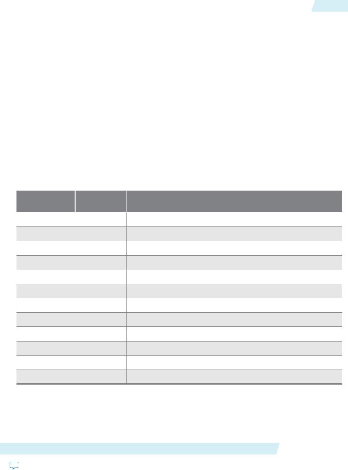
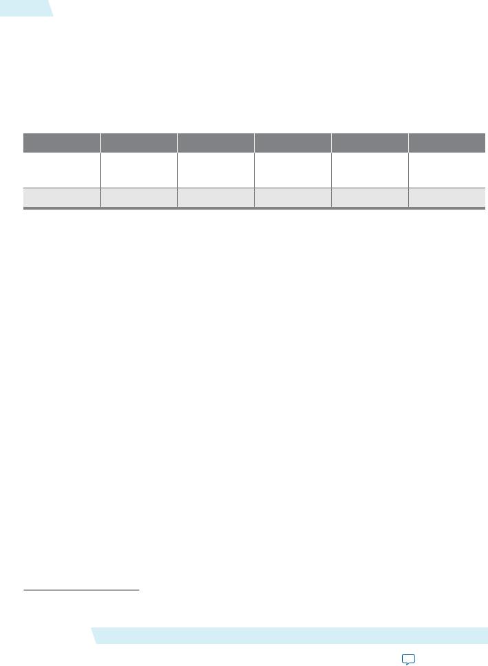
Total Number of PLL Available in Each Supported Device Family
The following table lists the total number of PLLs available for configuration and the PLL types supported by the ALTPLL IP core for each device family.
Table 1: Total Number of PLLs per Device Family
Device Family |
Total Number of |
PLL Types |
|
PLLs |
|
Arria GX |
8 |
Enhanced and Fast |
Arria II GX |
6 |
Left_Right |
Stratix IV |
12 |
Top_Bottom and Left_Right |
Stratix III |
12 |
Top_Bottom and Left_Right |
Stratix II |
12 |
Enhanced and Fast |
Stratix II GX |
8 |
Enhanced and Fast |
Stratix |
12 |
Enhanced and Fast |
Stratix GX |
8 |
Enhanced and Fast |
Cyclone IV |
4 |
Cyclone IV PLL |
Cyclone III |
4 |
Cyclone III PLL |
Cyclone II |
4 |
Cyclone II PLL |
Cyclone |
2 |
Cyclone PLL |
Operation Modes
The ALTPLL IP core supports up to five different clock feedback modes, depending on the selected device family. Each mode allows clock multiplication and division, phase shifting, and duty-cycle programming.
ALTPLL (Phase-Locked Loop) IP Core User Guide |
Altera Corporation |
Send Feedback
4 |
Operation Modes Supported in Each Device Family |
ug-altpll |
|
2014.08.18 |
|||
|
|
The following list describes the operation modes for the ALTPLL IP core:
•Normal mode—The PLL feedback path source is a global or regional clock network, minimizing clock delay to registers for that clock type and specific PLL output. You can specify PLL output that is compensated in normal mode.
•Source-Synchronous mode—The data and clock signals arrive at the same time at the data and clock input pins. In this mode, the signals are guaranteed to have the same phase relationship at the clock and data ports of any Input Output Enable register.
•Zero-Delay Buffer mode—The PLL feedback path is confined to the dedicated PLL external clock output pin. The clock port driven off-chip is phase aligned with the clock input for a minimal delay between the clock input and the external clock output.
•No Compensation mode—The PLL feedback path is confined to the PLL loop. It has no clock network or other external source. A PLL in no-compensation mode has no clock network compensation, but clock jitter is minimized.
•External Feedback mode—The PLL compensates for the fbin feedback input to the PLL. The delay between the input clock pin and the feedback clock pin is minimized.
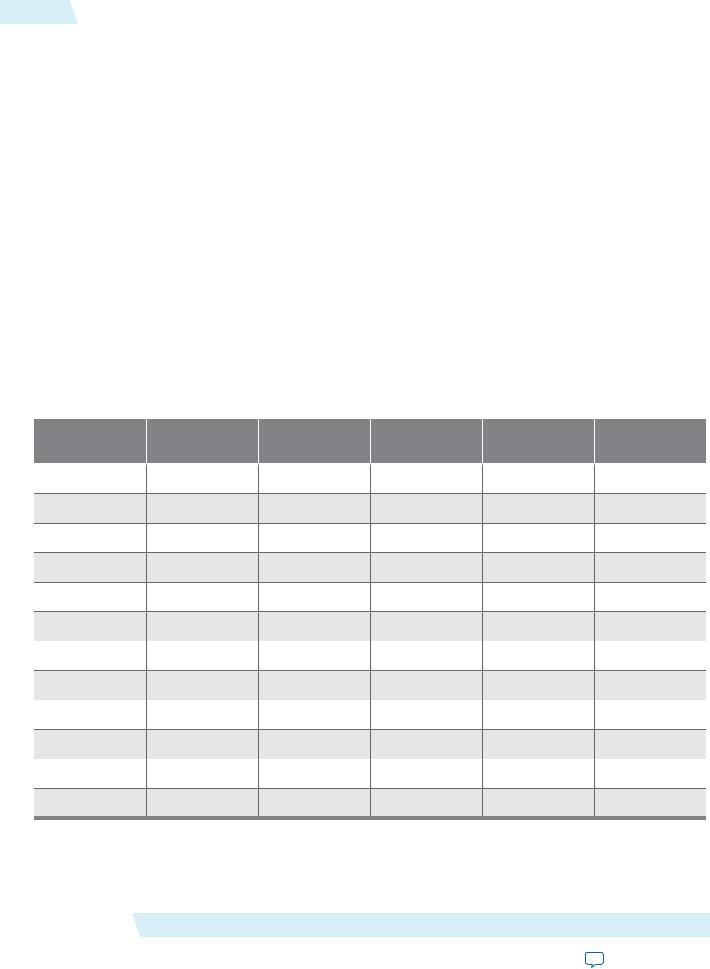
Operation Modes Supported in Each Device Family
The following table summarizes the operation modes supported for each device family.
Table 2: PLL Types and Modes Supported in Different Device Families
Device Family |
Normal |
Source- |
Zero-Delay Buffer |
No Compensation |
External Feedback |
|
|
Synchronous |
|
|
|
Arria GX |
All PLL types |
All PLL types |
Enhanced PLL |
All PLL types |
Enhanced PLL |
Arria II GX |
Left_Right PLL |
Left_Right PLL |
Left_Right PLL |
Left_Right PLL |
— |
Stratix IV |
All PLL types |
All PLL types |
All PLL types |
All PLL types |
All PLL types |
Stratix III |
All PLL types |
All PLL types |
Enhanced PLL |
All PLL types |
Enhanced PLL |
Stratix II |
All PLL types |
All PLL types |
Enhanced PLL |
All PLL types |
Enhanced PLL |
Stratix II GX |
All PLL types |
All PLL types |
Enhanced PLL |
All PLL types |
Enhanced PLL |
Stratix |
All PLL types |
— |
Enhanced PLL |
All PLL types |
Enhanced PLL |
Stratix GX |
All PLL types |
— |
Enhanced PLL |
All PLL types |
Enhanced PLL |
Cyclone IV |
All PLL types |
All PLL types |
All PLL types |
All PLL types |
— |
Cyclone III |
All PLL types |
All PLL types |
All PLL types |
All PLL types |
— |
Cyclone II |
All PLL types |
All PLL types |
All PLL types |
All PLL types |
— |
Cyclone |
All PLL types |
— |
All PLL types |
All PLL types |
— |
Parameter Settings
Describes how to set the operation mode for the PLL using the ALTPLL parameter editor. The parameter settings are located on the General/Modes page of the ALTPLL parameter editor.
Altera Corporation |
ALTPLL (Phase-Locked Loop) IP Core User Guide |
Send Feedback
ug-altpll |
Parameter Settings |
5 |
|
2014.08.18 |
|||
|
|
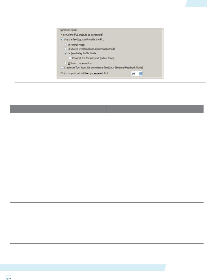
The following figure shows the options you can select from the page.
Figure 2: Operation Mode Options
The following table lists the options you can select from the page.
Table 3: Operation Mode Options and Descriptions
Option |
Description |
Use the feedback path inside the PLL |
Specify which operation mode to use. |
For source-synchronous mode, zero-delay buffer mode, and external feedback mode, you must make PLL Compensation assignments using the Assignment Editor in addition to setting the appropriate mode in the IP core. The assignment allows you to specify an output pin as a compensation target for a PLL in zerodelay buffer mode or external feedback mode, or to specify an input pin or group of input pins as compensation targets for a PLL in source-synchronous mode.
Create an 'fbin' input for an external feedback (External Feedback Mode)
Select this option to set the PLL in external feedback mode. The fbin port is the input port to the PLL from the external feedback path. In this mode, the PLL compensates for the fbin port. The delay between the input clock pin and the feedback clock pin is minimized.
Which output clock will be compensated for?
Specify which output port of the PLL is to be compensated for. The drop down list contains all output clock ports for the selected device. The correct output clock selection depends on the operation mode that you select. For example, for normal mode, select the core output clock. For zero-delay buffer mode or external feedback mode, select the external output clock.
The following figure shows the options you can select from the page.
ALTPLL (Phase-Locked Loop) IP Core User Guide |
Altera Corporation |
Send Feedback
6 |
Determining the PLL Lock Range |
ug-altpll |
|
2014.08.18 |
|||
|
|
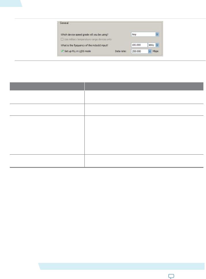
Figure 3: General Options
The following table lists the options you can select from the page.
Table 4: Operation Mode Options and Descriptions
Option
Which device speed grade will you be using?
What is the frequency of the inclock0 input?
Description
Specify the speed grade if you are not already using a device with the fastest speed. The lower the number, the faster the speed grade.
Specify the frequency of the input clock signal.
Set up PLL in LVDS mode |
Select this option when you want the PLL to supply the necessary |
|
clocking signals to the LVDS transmitter or receiver. In this mode, |
|
the PLL type and operation mode are forced to fast PLL and normal |
|
mode, respectively. This option creates two new output ports |
|
—sclkout and enable. |
|
This option is available only for the Arria GX, Stratix II, |
|
Stratix II GX, andHardCopy II device families. |
Data rate |
Specify the data rate for the PLL in LVDS mode. This option is |
|
available only if Set up PLL in LVDS mode is enabled. |
Determining the PLL Lock Range
The PLL lock range is the range between the minimum (Freq min lock parameter) and maximum (Freq min lock parameter) input frequency values for which the PLL can achieve lock. The Quartus II software shows these input frequency values in the PLL Summary report located under Resource Section of the Fitter folder in the Compilation Report. Changing the input frequency may cause the PLL to lose lock, but while the input clock remains within the minimum and maximum frequency specifications, the PLL is able to achieve lock.
Expanding the PLL Lock Range
The Quartus II software does not necessarily pick values for the PLL parameters to maximize the lock range. For example, you specify a 75 MHz input clock in the ALTPLL parameter editor, the actual PLL lock range may be between 70 MHz to 90 MHz. If your application requires a lock range of 50 MHz to 100 MHz, the default lock range of this PLL is insufficient.
For devices that support clock switchover in PLLs, you can use the ALTPLL parameter editor to maximize the lock range.
Altera Corporation |
ALTPLL (Phase-Locked Loop) IP Core User Guide |
Send Feedback

ug-altpll 2014.08.18
Setting Up Stratix III and Stratix IV PLLs for LVDS Interfacing |
7 |
To extract valid parameter values to maximize your PLL lock range, perform the following steps:
1.In the schematic editor, double-click the ALTPLL instance in your design to open the ALTPLL parameter editor.
2.For What is the frequency of your inclock0 input?, type the value of the low end of your desired PLL lock range. For example, if your application requires a lock range of 50 MHz to 100 MHz, type 50 MHz.
3.Turn on Create output file(s) using the 'Advanced' PLL parameters.
4.Turn on Create an 'inclk1' for a second inclk and enter the high end of your lock range as the frequency for inclk1. For example, if your application requires a lock range of 50 MHz to 100 MHz, type 100 MHz.
5.Complete the remaining pages in the ALTPLL parameter editor.
6.Compile your project and note the lock range shown in the PLL Summary report. If it is satisfactory, note all of the values for the PLL from this report, such as the M value, N value, charge pump current, loop filter resistance, and loop filter capacitance.
7.In the schematic editor, double-click the ALTPLL instance in your design to open the ALTPLL parameter editor.
8.Turn off Create an 'inclk1' for a second inclk.
9.Click Finish to update the PLL wrapper file.
10.In a text editor, open the PLL wrapper file. If the wrapper file is in Verilog format, go to the defparam section. If the wrapper file is in VHDL HDL, go to the generic map section. Modify all of the values for the parameters listed in step 6. Save the changes.
11.Compile your project.
12.Check the PLL Summary report to confirm the PLL lock range meets your requirements. The modified PLL should have the desired lock range.
If your input clock frequency is too close to the end of the desired PLL lock range—for example the low end of the desired lock range is 50 MHz and the input clock frequency is 50 MHz, the PLL might not maintain lock when the input clock has jitter or the frequency drifts below 50 MHz. You may choose to expand your PLL lock range to ensure your expected input clock frequency is further from the end of the range. For this example, you can enter 45 MHz and 105 MHz to ensure that your target lock range of 50 MHz to 100 MHz is within the PLL lock range.
The Quartus II software prompts an error message if it is unable to implement your preferred lock range using this procedure. Therefore, you have to look into other options, such as PLL reconfiguration to support your input frequency range.
Setting Up Stratix III and Stratix IV PLLs for LVDS Interfacing
The ALTLVDS IP core provides SERDES transmitter and receiver functionality commonly used in LVDS interfacing.
The following table lists the options and values to configure a PLL on a Stratix III or Stratix IV device to clock an ALTLVDS IP core.
Table 5: Options to Configure a PLL on a Stratix III or Stratix IV Device
Option  Value
Value
Which PLL type will you be |
Left_Right PLL |
|
using? |
|
|
How will the PLL outputs be |
In Source-Synchronous Compensation mode |
|
generated? |
|
|
ALTPLL (Phase-Locked Loop) IP Core User Guide |
Altera Corporation |
|
Send Feedback |
|
|

8Simulating External Feedback Board Delay
Option |
|
On the Output clocks page |
c0 |
|
This clock signal is |
|
the high-speed serial |
|
clock (fast clock) |
|
signal connected to |
|
the rx_inclock or |
|
tx_inclock port of |
|
the ALTLVDS IP |
|
core. |
|
Output frequency = |
|
data rate |
|
Phase shift = -180 |
|
degrees |
|
Duty cycle = 50% |
ug-altpll 2014.08.18
Value
c1 |
c2 |
This clock signal is the load enable signal connected to the rx_
enable or tx_enable port of the ALTLVDS IP core.
Output frequency = data rate/deserialization factor
Phase shift = [(deserialization factor – 2)/deserialization factor] × 360 degrees
Duty cycle = (100/ deserialization factor)
%
This clock signal is the slow clock signal that feeds the synchronization register of the ALTLVDS IP core.
Output frequency = data rate/ deserialization factor
Phase shift = (-180/deserializa- tion factor) degrees
Duty cycle = 50%
Related Information
SERDES Transmitter/Receiver (ALTLVDS) IP Core User Guide
Simulating External Feedback Board Delay
The PLL external feedback board delay option is available for Arria GX, Cyclone, HardCopy series, Stratix, Stratix GX, Stratix II, and Stratix II GX device families only.
The functional and timing models of these devices do not support the simulation of external feedback. To simulate the external feedback mode, perform the following steps:
1.In the Quartus II software, open an existing project or create a new project.
2.On the Assignments menu, click Assignment Editor.
3.In the Category bar, under Timing, click All.
4.In the spreadsheet, double-click an empty row in the To cell and either type in the pin name or click the arrow to use the Node Finder to search for the external feedback input pin.
5.Double-click the Assignment Name cell, and select PLL External Feedback Board Delay.
6.In the Value cell, double-click and type the amount of time for the signal to propagate between the external clock output pin through the trace on the board and into the external feedback input pin.
7.Simulate your design.
The behavioral models for the ALTPLL IP core reside in the \quartus\eda\sim_lib directory. The altera_mf.vhd file contains the VHDL behavioral models and the altera_mf.v file contains the Verilog HDL behavioral models. The behavioral model does not perform parameter error checking, so you must specify valid values.
Altera Corporation |
ALTPLL (Phase-Locked Loop) IP Core User Guide |
Send Feedback
ug-altpll |
Output Clocks |
9 |
|
2014.08.18 |
|||
|
|
Output Clocks
The PLL can generate a number of clock output signals depending on the PLL type and the device family that you select in the ALTPLL parameter editor. For example, in a Stratix IV device, a Left_Right PLL can generate seven clock output signals, and a Top_Bottom PLL can generate as many as 10 clock output signals. The generated clock output signals are used to clock the core or external blocks outside of the core.
The ALTPLL IP core does not have a dedicated output enable port, you can disable the PLL output. You can use the pllena signal or the areset signal to disable the PLL output counters, and thereby disable the PLL output clocks. Another possible method is to feed the PLL output clock signals to the ALTIOBUF IP core and use the enable output ports of the resulting buffers to disable the signals.
Parameter Settings
The Output Clocks page of the ALTPLL parameter editor contains the parameter settings for the clock output signals. The output clock port can be used as a core output clock or an external output clock port. The core output clock is used to feed the FPGA core and the external output clock is used to feed the dedicated pins on the FPGA.
The following figure shows a screenshot of the page to configure the c0 clock output signal of the ALTPLL IP core.
Figure 4: Output Clocks
ALTPLL (Phase-Locked Loop) IP Core User Guide |
Altera Corporation |
Send Feedback

10 |
Parameter Settings |
ug-altpll |
|
2014.08.18 |
|||
|
|
Each option has the following two columns:
•Requested settings
•Actual settings
The requested settings are the settings that you want to implement, and the actual settings are the settings closest values that can be implemented in the PLL circuit to best approximate the requested settings. Use the values in the actual settings column as a guide to adjust the requested settings. If the requested settings for one of the output clocks cannot be approximated, the ALTPLL parameter editor produces a warning message at the top of every page. To determine the output clocks that contain unachievable settings, turn on Per Clock Feasibility Indicators at the bottom of the ALTPLL parameter editor. The output clock name in red is the name of the clock with unachievable settings. The clock listed in green has no settings issues, and the grayed-out names are the unselected output clocks. You must adjust the requested settings for the affected output clocks to resolve the warning messages, or use another Altera device that meets your desired timing specifications.
To generate an output clock port in your ALTPLL IP core variation, select Use this clock.The output clock port that is to be compensated for is enabled by default. It cannot be disabled, unless you select a different output clock port to be compensated for.
The rest of the options on the page allow you to set the following output clock values:
•frequency
•phase shift
•duty cycle
The phase shift option allows you to set the programmable phase shift for an output clock signals. The smallest phase shift is 1/8th of VCO period. For degree increments, the maximum step size is 45 degrees. You can set smaller steps using the clock multiplication and division factors options. For example, if the post-scale counter is 32, the smallest phase shift step is 0.1°. The up and down buttons let you cycle through phase shift values. Alternatively, you can enter a number in the phase shift field manually instead of using the buttons.
Instead of specifying frequency of the output clock signal, you can also specify the multiplication and division factors of the signal in the requested settings column.
The following figure shows the formula for an output clock frequency.
Figure 5: PLL Output Clock Frequency
The ALTPLL parameter editor calculates the simplest fraction, and displays it in the actual settings column. For example, if the input clock frequency is 100 MHz, and the requested multiplication and division factors are 205 and 1025 respectively, the output clock frequency is calculated as 100 × 205/1025=20 MHz. The actual settings reflect the simplest fraction — the actual multiplication factor is 1, and the actual division factor is 5. You can use the copy button to copy values from the actual settings to the requested settings.
The actual values of multiplication and division factors are affected when you select Use these clock settings for the DPA clock or Set up PLL in LVDS mode.
Altera Corporation |
ALTPLL (Phase-Locked Loop) IP Core User Guide |
Send Feedback
ug-altpll 2014.08.18
Parameter Settings When “Set up PLL in LVDS mode” Option is Enabled |
11 |
Select Use these clock settings for the DPA clock if you want the output clock signal of the PLL to drive the input clock port of the DPA block in the ALTLVDS IP core. This option is available only for Stratix III and Stratix IV devices.
Parameter Settings When “Set up PLL in LVDS mode” Option is Enabled
The following parameter settings apply only when Set up PLL in LVDS Mode is turned on for Arria GX, Stratix II, Stratix II GX, and HardCopy II fast PLLs.
When you turn on Set up PLL in LVDS mode, two additional options are available on the Output Clocks pages for c0 and c1.
The following figure shows the additional options to configure the c0 output clock signal.
Figure 6: Additional Options to Configure the c0 Output Clock Signal
Turn on Create sclkout0/enable0 outputs to create the sclkout0 and enable0 ports. The sclkout0 port is the serial clock output port, and the enable0 port is the enable port.
The following figure shows the additional options to configure the c0 output clock signal.
Figure 7: Sclkout Phase Shift Option
The sclkout phase shift option allows you to edit the phase shift of the sclkout signal (in this case, the sclkout0 signal).
Only two pairs of sclkout and enable ports can be created in an ALTPLL IP core. The sclkout0 and enable0 ports are for the c0 output clock, and the sclkout1 and enable1 ports are for the c1 output clock.
Summary of PLL Output Clocks
The following table summarizes and compares properties of the clock output ports per PLL for each PLL type in the supported device families. The number of clock output ports shown in the table for each device family can be set as internal or external clock output port unless described otherwise.
Table 6: Number of Clock Output Ports per PLL
Device Family |
Top_Bottom |
Left_Right |
Enhanced PLL |
Fast PLL |
Cyclone Series PLL |
Arria GX |
— |
— |
6 |
4 |
— |
Arria II GX |
— |
7 |
— |
— |
— |
Stratix IV |
10 |
7 |
— |
— |
— |
Stratix III |
10 |
7 |
— |
— |
— |
Stratix II |
— |
— |
6 |
4 |
— |
ALTPLL (Phase-Locked Loop) IP Core User Guide |
|
|
|
Altera Corporation |
|
Send Feedback |
|
|
|
|
|

12 |
Advanced Features |
ug-altpll |
|
2014.08.18 |
|||
|
|
Device Family |
Top_Bottom |
Left_Right |
Enhanced PLL |
Fast PLL |
Cyclone Series PLL |
Stratix II GX |
— |
— |
6 |
4 |
— |
Stratix |
— |
— |
6 |
3 |
— |
|
|
(1) |
|
|
|
|
|
|
|
|
|
Stratix GX |
— |
— |
6 |
3 |
— |
|
|
(1) |
|
|
|
|
|
|
|
|
|
Cyclone IV |
— |
— |
— |
— |
5 |
Cyclone III |
— |
— |
— |
— |
5 |
Cyclone II |
— |
— |
— |
— |
3 |
Cyclone |
— |
— |
— |
— |
2 |
|
|
|
|
(2) |
|
|
|
|
|
|
Advanced Features
Altera devices offer on-chip PLL features previously found only in high-end discrete PLL devices. These advanced features, including gated lock, clock switchover, dynamic reconfiguration, programmable bandwidth, reconfigurable bandwidth, spread spectrum clocking, and post-scale counter cascading, increase system and device performance and provide advanced clock interfacing. The following sections define each advanced feature, and describe its application, and the parameter settings you must select in the ALTPLL parameter editor to enable the feature.
Advanced Control Signals (pllena, areset, pfdena)
You can use these three signals—pllena, areset, and pfdena—to observe and control PLL operation and resynchronization.
pllena
Use the pllena signal to enable or disable the PLL. When you deassert the pllena signal, the PLL does not drive any output clock signal and therefore it loses lock. All counters in the PLL, including the gated lock counter, return to the default state. When you assert the pllena signal, the PLL drives output clock signals and tries to gain lock. The single PLL enable port on each device is shared among all PLLs on the device. By default, the pllena signal is tied to VCC internally.
areset
The areset signal is the reset or resynchronization input for each PLL. The device input pin or internal logic can drive the areset signal. When you assert the areset signal, all counters in the PLL, including the gated lock counter, are reset to initial values, in which the PLL output is cleared and the PLL is in the out- of-lock state. The VCO is also reset to its nominal setting. When the areset signal is deasserted, the PLL resynchronizes its input and tries to gain lock.
(1)Only four ports can be used as the external clock output ports.
(2)Only one port can be used as the external clock output port.
Altera Corporation |
ALTPLL (Phase-Locked Loop) IP Core User Guide |
Send Feedback
ug-altpll 2014.08.18
pfdena 13
You should include the areset signal in your designs if any of the following conditions hold:
•PLL reconfiguration or clock switchover is enabled in your design.
•Phase relationships between the PLL input and output clocks must be maintained after a loss-of-lock condition.
•The input clock to the PLL is not toggling or is unstable at power-up.
•Assert the areset signal after the input clock is toggling while staying within the input jitter specification.
pfdena
The pfdena signal enables or disables the PFD circuit. The PFD circuit is enabled by default. When the PFD circuit is disabled, the PLL output does not depend on the input clock, and tends to drift outside of the lock window. By default, the pfdena signal is tied to VCC internally.
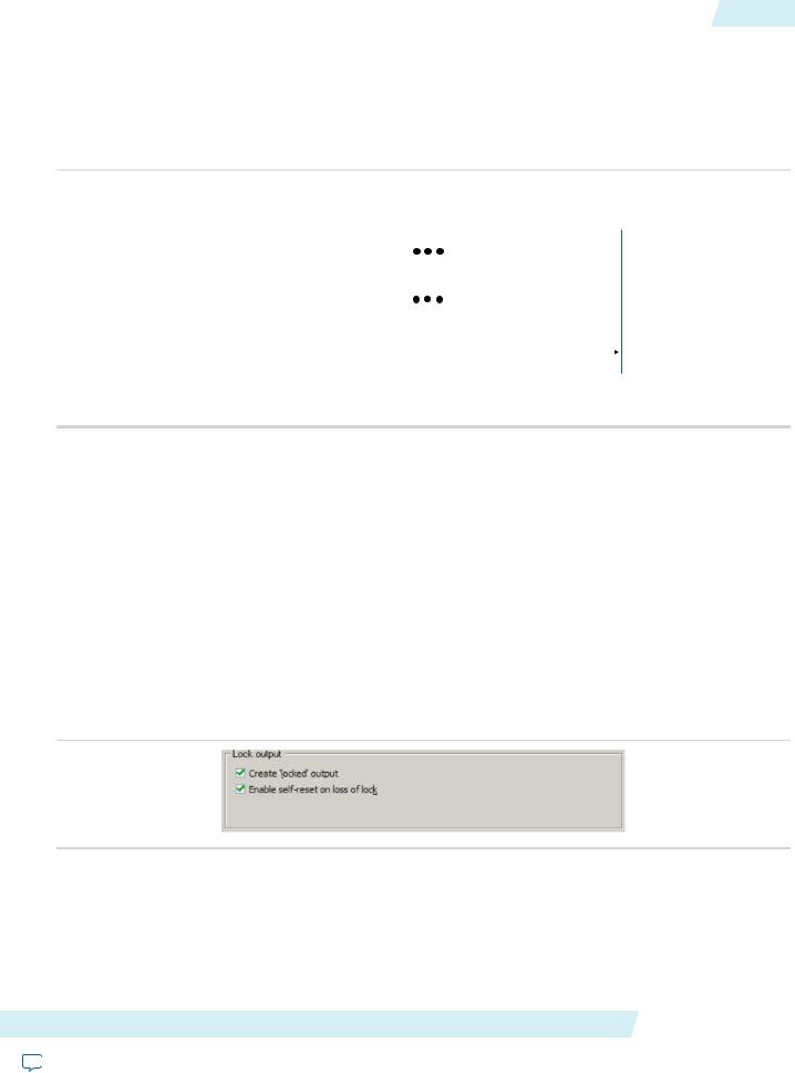
Parameter Settings
For devices that support the advanced control signals—pllena, pfdena, and areset, the parameter settings for these signals are located on the Inputs/Lock or Scan/Inputs/Lock page of the ALTPLL parameter editor.
The following figure shows the options related to the advanced control signals. Turn on the control signal you want to create from the options available.
Figure 8: Options to Select the Advanced Control Signals
The deassertion of the pllena signal or the assertion of the areset signal does not disable the VCO, but instead resets the VCO to its nominal value. The only time that the VCO is completely disabled is when you do not have a PLL instantiated in your design.
Summary of Advanced Control Signals
The following table summarizes the device families support for advanced control signals.
Device Family |
|
Supported Advanced Signals |
|
|
pllena |
pfdena |
areset |
Arria GX |
Yes |
Yes |
Yes |
Arria II GX |
— |
Yes |
Yes |
Stratix IV |
— |
Yes |
Yes |
Stratix III |
— |
Yes |
Yes |
Stratix II |
Yes |
Yes |
Yes |
Stratix II GX |
Yes |
Yes |
Yes |
Stratix |
Yes |
Yes |
Yes |
ALTPLL (Phase-Locked Loop) IP Core User Guide |
|
|
Altera Corporation |
Send Feedback |
|
|
|

14 |
Clock Switchover |
|
|
ug-altpll |
|
|
2014.08.18 |
||
|
|
|
|
|
|
Device Family |
|
Supported Advanced Signals |
|
|
|
pllena |
pfdena |
areset |
|
Stratix GX |
Yes |
Yes |
Yes |
|
Cyclone IV |
— |
Yes |
Yes |
|
Cyclone III |
— |
Yes |
Yes |
|
Cyclone II |
Yes |
Yes |
Yes |
|
Cyclone |
Yes |
Yes |
Yes |
Clock Switchover
The clock switchover feature allows the PLL to switch between two input clocks. The clock switchover feature can be used for switching between clock inputs of different frequencies and is also useful for video applications that require a manual switch between operation frequencies. The clock switchover capability is widely implemented in telecommunication, storage, and server markets because these markets require highly reliable clocking schemes to ensure system reliability.
The following clock switchover modes are supported by the ALTPLL IP core:
•Automatic switchover—The PLL monitors the currently used clock signal, and if it stops toggling or loss-of-lock occurs, the PLL automatically switches to the other clock signal (inclk0 or inclk1).
•Manual clock switchover—The clock switchover is controlled using the clkswitch signal. The manual override feature available in automatic clock switchover is different from the manual clock switchover.
Parameter Settings
For devices that support the clock switchover feature, the parameter settings are located on the Clock switchover page of the ALTPLL parameter editor.
The following figure shows all the options available on the Clock switchover page for an Arria GX device. The options are device-dependent and what you see may differ.
Altera Corporation |
ALTPLL (Phase-Locked Loop) IP Core User Guide |
Send Feedback
ug-altpll |
Parameter Settings |
15 |
|
2014.08.18 |
|||
|
|
Figure 9: Clock Switchover
To enable the switchover feature, turn on Create an 'inclk1' input for a second input clock, and specify the frequency of the inclk1 signal. The inclk0 signal is by default the primary input clock signal of the ALTPLL IP core.
Select the related option for manual or automatic clock switchover mode. For the automatic clock switchover mode, you can choose to create the clkswitch signal as a manual override. The automatic switchover is initiated during loss of lock or when the inclk0 signal stops toggling or when the clkswitch signal is asserted. You must specify the number of clock cycles to wait before the PLL performs the clock switchover. Note that the allowed number of clock cycles to wait is device-dependant.
You can use the optional signals – activeclock, clkloss, and clkbad—as indicators when you use the clock switchover feature.
Use the activeclock signal to monitor which input clock signal is driving the PLL. When the current clock signal is inclk0, the activeclock signal is low. When the current clock signal is inclk1, the activeclock signal is high.
Use the clkbad signals (clkbad0 and clkbad1) to monitor which input clock signal has stopped toggling. The clkbad0 signal is used to monitor the inclk0 signal, and the clkbad1 signal monitors the inclk1 signal. The clkbad0 signal goes high when the inclk0 signal stops toggling, and the clkbad1 signal goes high when the inclk1 signal stops toggling. The clkbad signals remain low when the input clock signals are toggling.
Use the clkloss signal to monitor the current status of the clock switchover. The clkloss signal goes high to indicate that loss of lock has been detected, and the clock switchover is initiated. The clkloss signal remains low when the clock switchover is not initiated. The clkloss signal is only available in Arria GX, Stratix, Stratix GX, Stratix II, and Stratix II GX devices.
The following top-level ports are created from these parameter settings:
•Input ports: inclk1 and clkswitch.
•Output ports: activeclock, clkloss, clkbad0, and clkbad1.
ALTPLL (Phase-Locked Loop) IP Core User Guide |
Altera Corporation |
Send Feedback

16 |
Summary of Automatic Clock Switchover Feature |
ug-altpll |
|
2014.08.18 |
|||
|
|
Summary of Automatic Clock Switchover Feature
The following table summarizes automatic clock switchover support in the supported device families. Also supports automatic clock switchover feature with manual override control.
Table 7: Automatic Clock Switchover Feature Support
Device Family |
Top_Bottom |
Left_Right |
Enhanced PLL |
|
Fast PLL Cyclone Series PLL |
Arria GX |
— |
— |
Yes |
No |
— |
Arria II GX |
— |
Yes |
— |
— |
— |
Stratix IV |
Yes |
Yes |
— |
— |
— |
Stratix III |
Yes |
Yes |
— |
— |
— |
Stratix II |
— |
— |
Yes |
No |
— |
Stratix II GX |
— |
— |
Yes |
No |
— |
Stratix |
— |
— |
Yes |
No |
— |
Stratix GX |
— |
— |
Yes |
No |
— |
Cyclone IV |
— |
— |
— |
— |
Yes |
Cyclone III |
— |
— |
— |
— |
Yes |
Cyclone II |
— |
— |
— |
— |
No |
Cyclone |
— |
— |
— |
— |
No |
The following table summarizes the manual clock switchover support in the supported device families.
Table 8: Manual Clock Switchover Feature Support
Device |
Top_Bottom |
Left_Right |
Enhanced PLL |
Fast PLL |
Cyclone Series PLL |
Arria GX |
— |
— |
Yes |
Yes |
— |
Arria II GX |
— |
Yes |
— |
— |
— |
Stratix IV |
Yes |
Yes |
— |
— |
— |
Stratix III |
Yes |
Yes |
— |
— |
— |
Stratix II |
— |
— |
Yes |
Yes |
— |
Stratix II GX |
— |
— |
Yes |
Yes |
— |
Stratix |
— |
— |
Yes |
No |
— |
Stratix GX |
— |
— |
Yes |
No |
— |
Cyclone IV |
— |
— |
— |
— |
Yes |
Altera Corporation |
|
|
ALTPLL (Phase-Locked Loop) IP Core User Guide |
||
|
|
|
|
|
Send Feedback |
ug-altpll |
|
|
|
|
Spread-Spectrum Clocking |
17 |
|
2014.08.18 |
|
|
|
|
|||
|
|
|
|
|
|
|
|
Device |
|
Top_Bottom |
Left_Right |
Enhanced PLL |
Fast PLL |
Cyclone Series PLL |
|
Cyclone III |
— |
— |
|
— |
— |
Yes |
|
Cyclone II |
— |
— |
|
— |
— |
Yes |
|
Cyclone |
— |
— |
|
— |
— |
No |
|
Spread-Spectrum Clocking
Spread-spectrum technology reduces electromagnetic interference (EMI) in a system. This technology works by distributing the clock energy over a broad frequency range.
The spread-spectrum clocking feature distributes the fundamental clock frequency energy throughout your design to minimize energy peaks at specific frequencies. By reducing the spectrum peak amplitudes, the feature makes your design more likely meets the EMI emission compliance standards, and reduces costs associated with traditional EMI containment.
The traditional methods for limiting EMI include shielding, filtering, and using multi-layer printed circuit boards. Multi-layer circuit boards are expensive and are not guaranteed to meet the EMI emission compliance standards. The use of spread-spectrum technology is simpler and more cost-effective than these other methods.
To use the spread-spectrum clocking feature, you must set the programmable bandwidth feature to Auto.
Parameter Settings
For devices that support spread-spectrum technology, the parameter settings are located on the Bandwidth/SS page of the ALTPLL parameter editor.
The following figure shows the Spread Spectrum window.
Figure 10: Spread Spectrum Settings
To enable the spread-spectrum feature, turn on Use spread spectrum feature. Set the desired down spread percentage, and the modulation frequency. The table in the spread spectrum window lists the detailed descriptions of the current counter values.
The down spread percentage defines the modulation width or frequency span of the instantaneous output frequency resulting from the spread spectrum. When you use down spread, the modulation width falls at or below a specified maximum output frequency. The wider the modulation, the larger the band of frequencies over which the energy is distributed, and the more reduction is achieved from the peak. For example, with a down spread percentage of 0.5% and maximum operating frequency of 100 MHz, the output frequency is swept between 99.5 and 100 MHz.
ALTPLL (Phase-Locked Loop) IP Core User Guide |
Altera Corporation |
Send Feedback
18 |
Summary of Spread-Spectrum Clocking Feature |
ug-altpll |
|
2014.08.18 |
|||
|
|
The modulation frequency, often called sweep rate, defines how fast the spreading signal sweeps from the minimum to the maximum frequency.
Turning on spread-spectrum clocking creates no new top-level ports.
Summary of Spread-Spectrum Clocking Feature
The following table summarizes the PLL types that support the spread-spectrum clocking feature.
Table 9: Spread-Spectrum Clocking Feature
Device  Top_Bottom
  Left_Right
  Enhanced PLL
  Fast PLL
  Cyclone Series PLL
Stratix IV |
Yes |
Yes |
— |
— |
— |
|
(3) |
(3) |
|
|
|
Cyclone IV |
— |
— |
— |
— |
No |
Gated Lock and Self-Reset
The lock time of a PLL is defined as the amount of time required by the PLL to attain the target frequency and phase relationship after device power-up, after a change in the PLL output frequency, or after resetting the PLL.
A PLL might lose lock for a number of reasons, such as the following causes:
•Excessive jitter on the input clock.
•Excessive switching noise on the clock inputs of the PLL.
•Excessive noise from the power supply can cause high output jitter and possible loss of lock.
•A glitch or stopping of the input clock to the PLL.
•Resetting the PLL by asserting the areset or pllena ports of the PLL.
•An attempt to reconfigure the PLL might cause the M counter, N counter, or phase shift to change, which causes the PLL to lose lock. However, changes to the post-scale counters do not affect the PLL locked signal.
•PLL input clock frequency drifts outside the lock range specification.
•The PFD is disabled using the pfdena port. When this happens, the PLL output phase and frequency tend to drift outside of the lock window.
The ALTPLL IP core allows you to monitor the PLL locking process using a lock signal named locked and also allows you to set the PLL to self-reset on loss of lock.
Gated Lock
Some devices support a gated lock signal that allows you to configure a programmable 20-bit counter that holds the lock signal low for a user-specified number of input clock transitions. This is useful to eliminate the false toggling of the lock signal as the PLL begins tracking the reference clock. Gated lock allows the PLL to lock before asserting the locked signal, providing a stabilized lock signal.
An asserted locked signal indicates the PLL clock output is aligned with the PLL reference input clock. The locked signal might toggle as the PLL begins tracking the reference clock. To avoid such a false lock indication,
(3)This device can accept a spread-spectrum input with typical modulation frequencies, but it cannot generate spread-spectrum clock signals internally.
Altera Corporation |
ALTPLL (Phase-Locked Loop) IP Core User Guide |
Send Feedback
ug-altpll 2014.08.18
Self-Reset on Loss of Lock |
19 |
use a gated lock signal. A gated locked signal or an ungated locked signal can feed a logic array or an output pin. When you must reset the gated counter, reset the PLL by asserting the areset signal or the pllena signal.
The following figure shows the timing waveform for gated and ungated locked signals.
Figure 11: Input and Output Ports
PLLENA |
|
|
|
|
|
|
|
|
|
|
|
|
|
|
|
|
|
|
|
|
|
|
|
|
|
|
|
|
|
|
|
|
|
|
|
|
|
|
|
|
|
|
|
|
|
|
|
|
|
|
|
|
|
|
|
|
|
|
|
|
|
|
|
|
|
|
|
|
|
|
|
|
|
|
|
|
|
|
|
|
|
|
|
|
|
|
|
|
|
Reference Clock |
|
|
|
|
|
|
|
|
|
|
|
|
|
|
|
|
|
|
|
|
|
|
|
|
|
|
|
|
|
|
|
|
|
|
|
|
|
|
|
|
|
|
|
|
|
|
|
|
|
|
|
|
|
|
|
|
|
|
|
Feedback Clock |
|
|
|
|
|
|
|
|
|
|
|
|
|
|
|
|
|
|
|
|
|
|
|
|
|
|
|
|
|
|
|
|
|
|
|
|
|
|
|
|
|
|
|
|
|
|
|
|
|
|
|
|
|
|
|
|
|
||
|
|
|
|
|
|
|
|
|
|
|
|
|
|
|
|
|
|
|
|
|
|
|
|
|
|
|
|
|
|
|
|
|
|
|
|
|
|
|
|
|
|
|
|
|
|
|
|
|
|
|
|
|
|
|
|
||||
Locked |
|
|
|
|
|
|
|
|
|
|
|
|
|
|
|
|
|
|
Filter Counter |
|
|
|
|||||||
|
|
|
|
|
|
|
|
|
|
|
|
|
|
|
|
|
|
|
|
|
Reaches |
|
|
|
|
|
|||
|
|
|
|
|
|
|
|
|
|
|
|
|
|
|
|
|
|
|
|
|
|
|
|
|
|||||
|
|
|
|
|
|
|
|
|
|
|
|
|
|
|
|
|
|
|
|
|
Value Count |
|
|
|
|||||
Gated Lock |
|
|
|
|
|
|
|
|
|
|
|
|
|
|
|
|
|
|
|
|
|
|
|||||||
|
|
|
|
|
|
|
|
|
|
|
|
|
|
|
|
|
|
|
|
|
|
|
|
|
|
|
|
||
|
|
|
|
|
|
|
|
|
|
|
|
|
|
|
|
|
|
|
|
|
|
|
|
|
|
|
|
||
|
|
|
|
|
|
|
|
|
|
|
|
|
|
|
|
|
|
|
|
|
|
|
|
|
|
|
|
|
|
Self-Reset on Loss of Lock
This feature allows the PLL to self-reset upon loss of lock, normally for the same reasons described in Gated Lock and Self-Reset on page 18
Related Information
Gated Lock and Self-Reset on page 18
Parameter Settings
To enable the locked signal, and the self-reset feature in the ALTPLL IP core, use the parameter settings on the Scan/Inputs/Lock or Inputs/Lock page of the ALTPLL parameter editor.
The following figure shows the related options in the Scan/Inputs/Lock or Inputs/Lock page for an Arria II GX device. Note that the options are device-dependent and what you see may differ.
Figure 12: Lock Output Options
Turning on Create 'locked' output creates an output port named locked in the ALTPLL IP core. Turning on Enable self-reset on loss of lock enables the self-reset feature.
In devices that support gated lock, another option appears on the page, which is the Hold 'locked' output option. Turning on this option enables the gated lock circuitry to gate the locked signal. You must specify the number of PLL input clock cycles to hold the locked signal low after the PLL is initialized. This value is used by the gated lock counter. The value ranges from 1 to 1,048,575 clock cycles.
ALTPLL (Phase-Locked Loop) IP Core User Guide |
Altera Corporation |
Send Feedback
20 |
Calculating the Value of Gated Lock Counter |
ug-altpll |
|
2014.08.18 |
|||
|
|
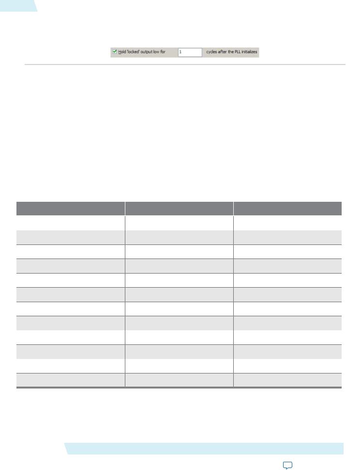
The following figure shows the Hold Locked Output option.
Figure 13: Hold Locked Output Option
Calculating the Value of Gated Lock Counter
To calculate the number of clock cycles needed, you must know the maximum lock time of the PLL, and the period of the PLL input clock. The lock time of the PLL is listed in the “PLL Timing Specifications” section of the DC & Switching Characteristics chapter of the device handbook. The period of the PLL input clock is user-specified. For example, if the maximum lock time of a PLL is 1 ms, and its input clock frequency is 100 MHz which corresponds to a 10 ns clock period, you calculate the value of the gated lock counter, by dividing 1 ms by 10 ns. The result is 100,000 clock cycles.
Only the locked port is created from these parameter settings.
Summary of Gated Lock Signals and Self-Reset on Loss of Lock
The following table summarizes the device families that support the gated lock and self-reset on loss of lock features.
Table 10: Gated Lock Signals and Self-Reset on Loss of Lock
Device Family |
|
Gated Lock Support |
Self-Reset on Loss of Lock |
Arria GX |
Yes |
|
— |
Arria II GX |
— |
|
Yes |
Stratix IV |
— |
|
Yes |
Stratix III |
— |
|
Yes |
Stratix II |
Yes |
|
— |
Stratix II GX |
Yes |
|
— |
Stratix |
— |
|
— |
Stratix GX |
— |
|
— |
Cyclone IV |
— |
|
Yes |
Cyclone III |
— |
|
Yes |
Cyclone II |
Yes |
|
— |
Cyclone |
— |
|
— |
Programmable Bandwidth
The PLL bandwidth is defined as the ability of the PLL to track the input clock and jitter. The bandwidth is measured by the -3 dB frequency of the closed-loop gain in the PLL, or approximately the unity gain point of the PLL open loop response. Altera devices provide a programmable PLL bandwidth feature that allows
Altera Corporation |
ALTPLL (Phase-Locked Loop) IP Core User Guide |
Send Feedback
ug-altpll 2014.08.18
Parameter Settings |
21 |
you to configure the characteristics of the PLL loop filter. Most loop filters contain only passive components, such as resistors and capacitors, which consumes board space. Altera FPGAs already contain these components, and by using the programmable bandwidth feature, you can control how the components affect the PLL bandwidth. This includes controlling the charge pump current, loop filter resistance, and high frequency capacitance values. The charge pump current affects the PLL bandwidth directly. The higher the charge pump current, the higher the PLL bandwidth.
Parameter Settings
The parameter settings to configure the bandwidth of the ALTPLL IP core are located on the Bandwidth/SS page of the ALTPLL parameter editor.
The following figure shows the bandwidth configuration options on the Bandwidth/SS page.
Figure 14: Bandwidth Configuration Options
The following list describes the preset values that you can choose:
•Low—PLL with a low bandwidth has better jitter rejection but a slower lock time.
•High—PLL with a high bandwidth has a faster lock time but tracks more jitter.
•Medium—A medium bandwidth offers a balance between lock time and jitter rejection.
If you select Auto, the ALTPLL parameter editor chooses the best possible bandwidth values to achieve the desired PLL settings. In some cases, you can get a bandwidth value outside the Low and High preset range.
To set the bandwidth manually, select Custom, and specify the value. The compiler attempts to achieve the value that you specify, or the closest possible value to achieve your desired setting. You can check the bandwidth value in the compilation report.
The table on the right in the Bandwidth/SS page shows the values of the charge pump current, loop filter resistance and capacitance, and the M counter.
An advanced level of control is also possible for precise control of the PLL loop filter characteristics. This level allows you to select the charge pump current, and loop filter resistance and capacitance values explicitly. The advanced parameters are: charge_pump_current, loop_filter_r, and loop_filter_c.
You can use the programmable bandwidth feature with the clock switchover or spread-spectrum features to get the PLL output settings that you desire. You must set the bandwidth to Auto if you want to enable the spread-spectrum feature.
These parameter settings create no additional top-level ports.
Summary of Programmable Bandwidth Support
The following table summarizes programmable bandwidth support in the different device families.
ALTPLL (Phase-Locked Loop) IP Core User Guide |
Altera Corporation |
Send Feedback
Loading...