


 Loading...
MAX 10 FPGA Configuration User Guide
Subscribe |
UG-M10CONFIG |
|
101 Innovation Drive |
|
|||
2015.05.04 |
|
San Jose, CA 95134 |
|
Send Feedback |
|
||
|
|
www.altera.com |
|
|
|
|
|

TOC-2
Contents
MAX 10 FPGA Configuration Overview............................................................ |
1-1 |
MAX 10 FPGA Configuration Schemes and Features....................................... |
2-1 |
Configuration Schemes............................................................................................................................... |
2-1 |
JTAG Configuration........................................................................................................................ |
2-1 |
Internal Configuration.................................................................................................................... |
2-2 |
Configuration Features............................................................................................................................... |
2-8 |
Remote System Upgrade in Dual Compressed Images.............................................................. |
2-8 |
Configuration Design Security..................................................................................................... |
2-15 |
SEU Mitigation and Configuration Error Detection................................................................ |
2-18 |
Configuration Data Compression............................................................................................... |
2-22 |
Configuration Details................................................................................................................................ |
2-23 |
Configuration Sequence................................................................................................................ |
2-23 |
MAX 10 Configuration Pins......................................................................................................... |
2-25 |
MAX 10 FPGA Configuration Design Guidelines............................................. |
3-1 |
Dual-Purpose Configuration Pins............................................................................................................. |
3-1 |
Guidelines: Dual-Purpose Configuration Pin.............................................................................. |
3-1 |
Enabling Dual-purpose Pin............................................................................................................ |
3-2 |
Configuring MAX 10 Devices using JTAG Configuration.................................................................... |
3-2 |
JTAG Configuration Setup............................................................................................................. |
3-3 |
ICB Settings in JTAG Configuration............................................................................................. |
3-4 |
Configuring MAX 10 Devices using Internal Configuration................................................................ |
3-4 |
Selecting Internal Configuration Modes...................................................................................... |
3-5 |
.pof and ICB Settings....................................................................................................................... |
3-5 |
Programming .pof into Internal Flash.......................................................................................... |
3-7 |
Accessing the Remote System Upgrade Block Through User Interface.............................................. |
3-8 |
Error Detection............................................................................................................................................ |
3-8 |
Verifying Error Detection Functionality...................................................................................... |
3-8 |
Enabling Error Detection................................................................................................................ |
3-9 |
Accessing Error Detection Block Through User Interface........................................................ |
3-9 |
Enabling Data Compression..................................................................................................................... |
3-10 |
Enabling Compression Before Design Compilation................................................................. |
3-11 |
Enabling Compression After Design Compilation................................................................... |
3-11 |
AES Encryption.......................................................................................................................................... |
3-11 |
Generating .ekp File and Encrypt Configuration File.............................................................. |
3-12 |
Generating .jam/.jbc/.svf file from .ekp file................................................................................ |
3-13 |
Programming .ekp File and Encrypted POF File...................................................................... |
3-14 |
Encryption in Internal Configuration......................................................................................... |
3-15 |
Altera Corporation

|
TOC-3 |
MAX 10 FPGA Configuration IP Core Implementation Guides...................... |
4-1 |
Altera Unique Chip ID IP Core................................................................................................................. |
4-1 |
Instantiating the Altera Unique Chip ID IP Core....................................................................... |
4-1 |
Resetting the Altera Unique Chip ID IP Core............................................................................. |
4-1 |
Altera Dual Configuration IP Core........................................................................................................... |
4-1 |
Instantiating the Altera Dual Configuration IP Core................................................................. |
4-2 |
Altera Dual Configuration IP Core References.................................................. |
5-1 |
Altera Dual Configuration IP Core Avalon-MM Address Map............................................................ |
5-1 |
Altera Dual Configuration IP Core Parameters...................................................................................... |
5-3 |
Altera Unique Chip ID IP Core References........................................................ |
6-1 |
Altera Unique Chip ID IP Core Ports....................................................................................................... |
6-1 |
Additional Information for MAX 10 FPGA Configuration User Guide.......... |
A-1 |
Document Revision History for MAX 10 FPGA Configuration User Guide..................................... |
A-2 |
Altera Corporation

MAX 10 FPGA Configuration Overview 1
2015.05.04
UG-M10CONFIG |
Subscribe |
Send Feedback |
You can configure MAX® 10 configuration RAM (CRAM) using the following configuration schemes:
•JTAG configuration—using JTAG interface.
•Internal configuration—using internal flash.
Supported Configuration Features
Table 1-1: Configuration Schemes and Features Supported by MAX 10 Devices
Configuration Scheme |
|
Remote System |
|
Compression |
|
Design Security |
|
SEU Mitigation |
|
Upgrade |
|
|
|
||||
|
|
|
|
|
|
|
|
|
|
|
|
|
|
|
|
|
|
JTAG configuration |
|
— |
|
— |
|
— |
|
Yes |
|
|
|
|
|
|
|
|
|
Internal configuration |
|
Yes |
|
Yes |
|
Yes |
|
Yes |
|
|
|
|
|
|
|
|
|
Related IP Cores
•Altera Dual Configuration IP Core—used in the remote system upgrade feature.
•Altera Unique Chip ID IP Core—retrieves the chip ID of MAX 10 devices.
Related Information
•MAX 10 FPGA Configuration Schemes and Features on page 2-1 Provides information about the configuration schemes and features.
•MAX 10 FPGA Configuration Design Guidelines on page 3-1
Provides information about using the configuration schemes and features.
•Altera Unique Chip ID IP Core on page 2-16
•Altera Dual Configuration IP Core on page 2-14
© 2015 Altera Corporation. All rights reserved. ALTERA, ARRIA, CYCLONE, ENPIRION, MAX, MEGACORE, NIOS, QUARTUS and STRATIX words and logos are trademarks of Altera Corporation and registered in the U.S. Patent and Trademark Office and in other countries. All other words and logos identified as trademarks or service marks are the property of their respective holders as described at www.altera.com/common/legal.html. Altera warrants performance of its semiconductor products to current specifications in accordance with Altera's standard warranty, but reserves the right to make changes to any products and services at any time without notice. Altera assumes no responsibility or liability arising out of the application or use of any information, product, or service described herein except as expressly agreed to in writing by Altera. Altera customers are advised to obtain the latest version of device specifications before relying on any published information and before placing orders for products or services.
ISO 9001:2008 Registered
www.altera.com
101 Innovation Drive, San Jose, CA 95134
|
MAX 10 FPGA Configuration Schemes and |
2 |
|
|
|
Features |
|
2015.05.04 |
|
|
|
UG-M10CONFIG |
Subscribe |
Send Feedback |
|
Configuration Schemes
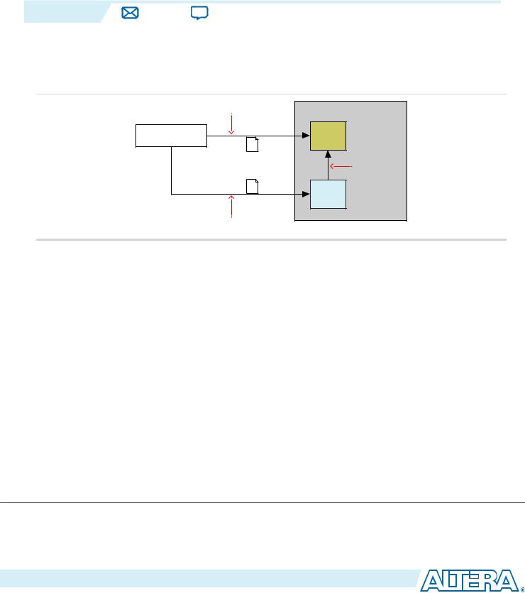
Figure 2-1: High-Level Overview of JTAG Configuration and Internal Configuration for MAX 10 Devices
JTAG Configuration |
MAX 10 Device |
|
|
Configuration Data |
CRAM |
.sof |
|
|
Internal |
|
Configuration |
.pof |
CFM |
|
|
JTAG In-System Programming |
|
JTAG Configuration
In MAX 10 devices, JTAG instructions take precedence over the internal configuration scheme.
Using the JTAG configuration scheme, you can directly configure the device CRAM through the JTAG interface—TDI, TDO, TMS, and TCK pins. The Quartus® II software automatically generates an SRAM Object File (.sof). You can program the .sof using a download cable with the Quartus II software programmer.
Related Information
Configuring MAX 10 Devices using JTAG Configuration on page 3-2
Provides more information about JTAG configuration using download cable with Quartus II software programmer.
© 2015 Altera Corporation. All rights reserved. ALTERA, ARRIA, CYCLONE, ENPIRION, MAX, MEGACORE, NIOS, QUARTUS and STRATIX words and logos are trademarks of Altera Corporation and registered in the U.S. Patent and Trademark Office and in other countries. All other words and logos identified as trademarks or service marks are the property of their respective holders as described at www.altera.com/common/legal.html. Altera warrants performance of its semiconductor products to current specifications in accordance with Altera's standard warranty, but reserves the right to make changes to any products and services at any time without notice. Altera assumes no responsibility or liability arising out of the application or use of any information, product, or service described herein except as expressly agreed to in writing by Altera. Altera customers are advised to obtain the latest version of device specifications before relying on any published information and before placing orders for products or services.
ISO 9001:2008 Registered
www.altera.com
101 Innovation Drive, San Jose, CA 95134

2-2 |
JTAG Pins |
|
|
|
UG-M10CONFIG |
|||
|
|
2015.05.04 |
||||||
|
|
|
|
|
|
|||
|
JTAG Pins |
|
|
|
|
|
||
Table 2-1: JTAG Pin |
|
|
|
|
|
|||
|
|
|
|
|
|
|
|
|
|
|
Pin |
|
|
Function |
|
Description |
|
|
|
|
|
|
|
|
|
|
|
|
TDI |
|
Serial input pin for: |
|
• TDI is sampled on the rising edge of TCK |
||
|
|
|
|
• |
instructions |
|
• TDI pins have internal weak pull-up resistors. |
|
|
|
|
|
• |
test data |
|
|
|
|
|
|
|
• |
programming data |
|
|
|
|
|
|
|
|
|
|
||
|
|
TDO |
|
Serial output pin for: |
|
• TDO is sampled on the falling edge of TCK |
|
|
|
|
|
|
• |
instructions |
|
• The pin is tri-stated if data is not shifted out |
|
|
|
|
|
• |
test data |
|
of the device. |
|
|
|
|
|
• |
programming data |
|
|
|
|
|
|
|
|
|
|
|
|
|
|
TMS |
|
Input pin that provides the control |
|
• TMS is sampled on the rising edge of TCK |
||
|
|
|
|
signal to determine the transitions of |
|
• TMS pins have internal weak pull-up resistors. |
||
|
|
|
|
the TAP controller state machine. |
|
|||
|
|
|
|
|
|
|
||
|
|
|
|
|
|
|
||
|
|
TCK |
|
Clock input to the BST circuitry. |
|
— |
|
|
|
|
|
|
|
|
|
|
|
All the JTAG pins are powered by the VCCIO 1B. In JTAG mode, the I/O pins support the LVTTL/ LVCMOS 3.3-1.5V standards.
Related Information
•MAX 10 Device Datasheet
Provides more information about supported I/O standard in MAX 10 devices.
•Guidelines: Dual-Purpose Configuration Pin on page 3-1
•Enabling Dual-purpose Pin on page 3-2
Internal Configuration
You need to program the configuration data into the configuration flash memory (CFM) before internal configuration can take place. The configuration data to be written to CFM will be part of the programmer object file (.pof). Using JTAG In-System Programming (ISP), you can program the .pof into the internal flash.
During internal configuration, MAX 10 devices load the CRAM with configuration data from the CFM.
Internal Configuration Modes
The internal configuration scheme for all MAX 10 devices except for 10M02 device consists of the following modes:
•Dual Compressed Images—configuration image is stored as image 0 and image 1 in the CFM
•Single Compressed Image
•Single Compressed Image with Memory Initialization
•Single Uncompressed Image
•Single Uncompressed Image with Memory Initialization
In dual compressed images mode, you can use the CONFIG_SEL pin to select the configuration image.
Altera Corporation |
MAX 10 FPGA Configuration Schemes and Features |
|
|
Send Feedback

UG-M10CONFIG |
Configuration Flash Memory |
2-3 |
|
2015.05.04 |
|||
|
|
The internal configuration scheme for 10M02 device supports the following mode:
•Single Compressed Image
•Single Uncompressed Image
Related Information
•Configuring MAX 10 Devices using Internal Configuration on page 3-4
•Remote System Upgrade in Dual Compressed Images on page 2-8
Configuration Flash Memory
The CFM is a non-volatile internal flash that is used to store configuration images. The CFM may store up to two compressed configuration images, depending on the compression and the MAX 10 devices. The compression ratio for the configuration image should be at least 30% for the device to be able store two configuration images.
Table 2-2: Maximum Number of Compressed Configuration Image for MAX 10 Devices
Device |
|
Maximum Number of Compressed Configuration Image |
|
|
|
10M02 |
|
1 |
|
|
|
10M04, 10M08, 10M16, 10M25, 10M40, and 10M50 |
|
2 |
|
|
|
Related Information
Configuration Flash Memory Permissions on page 2-18
Configuration Flash Memory Sectors
All CFM in MAX 10 devices consist of three sectors, CFM0, CFM1, and CFM2 except for the 10M02. The sectors are programmed differently depending on the internal configuration mode you select.
The 10M02 device consists of only CFM0. The CFM0 sector in 10M02 devices is programmed similarly when you select single compressed image or single uncompressed image.
MAX 10 FPGA Configuration Schemes and Features |
Altera Corporation |
|
|
Send Feedback

2-4 |
Configuration Flash Memory Total Programming Time |
UG-M10CONFIG |
|
2015.05.04 |
|||
|
|
Figure 2-2: Configuration Flash Memory Sectors Utilization for all MAX 10 Devices Except for the 10M02 Device
Unutilized CFM1 and CFM2 sectors can be used for additional user flash memory (UFM).
|
Internal Configuration |
|
Configuration Flash Memory Sectors |
|
|||||||||
|
|
|
|
|
|
|
|
|
|
|
|
|
|
|
Mode |
|
CFM2 |
|
|
CFM1 |
|
|
|
CFM0 |
|
||
|
|
|
|
|
|
|
|
|
|
|
|
|
|
|
|
|
|
|
|
|
|
|
|
|
|
|
|
|
Dual Compressed Image |
|
Compressed |
|
Image 1 |
|
|
|
|
Compressed Image 0 |
|
|
|
|
|
|
|
|
|
|
|
|
|
|
|
|
|
|
|
|
|
|
|
|
|
|
|
|
|
|
|
|
|
|
|
|
|
|
|
|
|
|
|
|
|
|
Single Uncompressed Image |
|
User Flash Memory |
|
|
|
|
Uncompressed Image 0 |
|
|
|||
|
|
|
|
|
|
|
|
|
|
|
|
|
|
|
|
|
|
|
|
|
|
|
|
|
|
|
|
|
Single Uncompressed Image |
|
|
|
|
|
|
|
|
|
|
|
|
|
|
Uncompressed Image 0 with Memory Initialization |
|
|
|||||||||
|
with Memory Initialization |
|
|
|
|||||||||
|
|
|
|
|
|
|
|
|
|
|
|
|
|
|
|
|
|
|
|
|
|
|
|
|
|
|
|
|
Single Compressed Image |
|
|
|
|
|
|
|
|
|
|
|
|
|
|
Compressed Image 0 with Memory Initialization |
|
|
|||||||||
|
with Memory Initialization |
|
|
|
|||||||||
|
|
|
|
|
|
|
|
|
|
|
|
|
|
|
|
|
|
|
|
|
|
|
|
|
|
|
|
|
|
|
|
|
|
|
|
|
|
|
|
|
|
|
Single Compressed Image |
|
User Flash Memory |
|
|
|
|
Compressed Image 0 |
|
|
|||
|
|
|
|
|
|
|
|
|
|
|
|
|
|
|
|
|
|
|
|
|
|
|
|
|
|
|
|
|
|
|
|
|
|
|
|
|
|
|
|
|
|
Related Information
CFM and UFM Array Size
Configuration Flash Memory Total Programming Time
Table 2-3: Configuration Flash Memory Total Programming Time for Sectors in MAX 10 Devices
Device |
|
|
|
Programming Time (s) |
|
|
|
|
|
|
|
|
|
|
CFM2 |
|
CFM1 |
|
CFM0 |
|
|
|
|
|
|||
|
|
|
|
|
|
|
10M02 |
|
— |
|
— |
|
5.4 |
|
|
|
|
|
|
|
10M04 |
|
6.5 |
|
4.6 |
|
11.1 |
|
|
|
|
|
|
|
10M08 |
|
12.0 |
|
8.9 |
|
20.8 |
|
|
|
|
|
|
|
10M16 and 10M25 |
|
16.4 |
|
12.6 |
|
29.0 |
|
|
|
|
|
|
|
10M40 and 10M50 |
|
30.2 |
|
22.7 |
|
52.9 |
|
|
|
|
|
|
|
In-System Programming
You can program the internal flash including the CFM of MAX 10 devices with ISP through industry standard JTAG interface. ISP offers the capability to program, erase, and verify the CFM. The JTAG circuitry and ISP instructions for MAX 10 devices are compliant to the IEEE-1532-2002 programming specification.
During ISP, the MAX 10 receives the IEEE Std. 1532 instructions, addresses, and data through the TDI input pin. Data is shifted out through the TDO output pin and compared with the expected data.
Altera Corporation |
MAX 10 FPGA Configuration Schemes and Features |
|
|
Send Feedback

UG-M10CONFIG |
Real-Time ISP |
2-5 |
|
2015.05.04 |
|||
|
|
The following are the generic flow of an ISP operation:
1.Check ID—the JTAG ID is checked before any program or verify process. The time required to read this JTAG ID is relatively small compared to the overall programming time.
2.Enter ISP—ensures the I/O pins transition smoothly from user mode to the ISP mode.
3.Sector Erase—shifting in the address and instruction to erase the device and applying erase pulses.
4.Program—shifting in the address, data, and program instructions and generating the program pulse to program the flash cells. This process is repeated for each address in the internal flash sector.
5.Verify—shifting in addresses, applying the verify instruction to generate the read pulse, and shifting out the data for comparison. This process is repeated for each internal flash address.
6.Exit ISP—ensures that the I/O pins transition smoothly from the ISP mode to the user mode.
You can also use the Quartus II Programmer to program the CFM.
Related Information
Programming .pof into Internal Flash on page 3-7
Provides the steps to program the .pof using Quartus II Programmer.
Real-Time ISP
In a normal ISP operation, to update the internal flash with a new design image, the device exits from user mode and all I/O pins remain tri-stated. After the device completes programing the new design image, it resets and enters user mode.
The real-time ISP feature updates the internal flash with a new design image while operating in user mode. During the internal flash programming, the device continues to operate using the existing design. After the new design image programming process completes, the device will not reset. The new design image update only takes effect in the next reconfiguration cycle.
ISP and Real-Time ISP Instructions
Table 2-4: ISP and Real-Time ISP Instructions for MAX 10 Devices
Instruction |
|
Instruction Code |
|
Description |
||
|
|
|
|
|
|
|
CONFIG_IO |
|
00 |
0000 |
1101 |
|
• Allows I/O reconfiguration through JTAG ports using |
|
|
|
|
|
|
the IOCSR for JTAG testing. This is executed after or |
|
|
|
|
|
|
during configurations. |
|
|
|
|
|
|
• nSTATUS pin must go high before you can issue the |
|
|
|
|
|
|
CONFIG_IO instruction. |
|
|
|
|
|
|
|
PULSE_NCONFIG |
|
00 |
0000 |
0001 |
|
Emulates pulsing the nCONFIG pin low to trigger reconfi |
|
|
|
|
|
|
guration even though the physical pin is unaffected. |
|
|
|
|
|
|
|
MAX 10 FPGA Configuration Schemes and Features |
Altera Corporation |
|
|
Send Feedback

2-6 |
ISP and Real-Time ISP Instructions |
|
UG-M10CONFIG |
|||||
2015.05.04 |
||||||||
|
|
|
|
|
||||
|
|
|
|
|
|
|
||
|
|
Instruction |
|
Instruction Code |
|
Description |
|
|
|
|
|
|
|
|
|
|
|
|
|
ISC_ENABLE_HIZ (1) |
|
10 1100 1100 |
|
• Puts the device in ISP mode, tri-states all I/O pins, |
||
|
|
|
|
|
|
and drives all core drivers, logic, and registers. |
||
|
|
|
|
|
|
• Device remains in the ISP mode until the ISC_ |
||
|
|
|
|
|
|
DISABLE instruction is loaded and updated. |
||
|
|
|
|
|
|
• The ISC_ENABLE instruction is a mandatory instruc |
||
|
|
|
|
|
|
tion. This requirement is met by the ISC_ENABLE_ |
||
|
|
|
|
|
|
CLAMP or ISC_ENABLE_HIZ instruction. |
||
|
|
|
|
|
|
|
||
|
|
ISC_ENABLE_CLAMP (1) |
|
10 0011 0011 |
|
• Puts the device in ISP mode and forces all I/O pins to |
|
|
|
|
|
|
|
|
follow the contents of the JTAG boundary-scan |
|
|
|
|
|
|
|
|
register. |
|
|
|
|
|
|
|
|
• When this instruction is activated, all core drivers, |
|
|
|
|
|
|
|
|
logics, and registers are frozen. The I/O pins remain |
|
|
|
|
|
|
|
|
clamped until the device exits ISP mode successfully. |
|
|
|
|
|
|
|
|
|
|
|
|
|
ISC_DISABLE |
|
10 0000 0001 |
|
• Brings the device out of ISP mode. |
||
|
|
|
|
|
|
• Successful completion of the ISC_DISABLE instruction |
||
|
|
|
|
|
|
happens immediately after waiting 200 µs in the Run- |
||
|
|
|
|
|
|
Test/Idle state. |
||
|
|
|
|
|
|
|
||
|
|
ISC_PROGRAM(2) |
|
10 1111 0100 |
|
Sets the device up for in-system programming. Program |
|
|
|
|
|
|
|
|
ming occurs in the run-test or idle state. |
|
|
|
|
ISC_NOOP(2) |
|
10 0001 0000 |
|
• Sets the device to a no-operation mode without |
||
|
|
|
|
|
|
leaving the ISP mode and targets the ISC_Default |
||
|
|
|
|
|
|
register. |
||
|
|
|
|
|
|
• Use when: |
||
|
|
|
|
|
|
• two or more ISP-compliant devices are being |
||
|
|
|
|
|
|
accessed in ISP mode and; |
||
|
|
|
|
|
|
• a subset of the devices perform some instructions |
||
|
|
|
|
|
|
while other more complex devices are completing |
||
|
|
|
|
|
|
extra steps in a given process. |
||
|
|
|
|
|
|
|
||
|
|
ISC_ADDRESS_SHIFT(2) |
|
10 0000 0011 |
|
Sets the device up to load the flash address. It targets the |
|
|
|
|
|
|
|
|
ISC_Address register, which is the flash address register. |
|
|
|
|
ISC_ERASE(2) |
|
10 1111 0010 |
|
• Sets the device up to erase the internal flash. |
|
|
|
|
|
|
|
|
• Issue after ISC_ADDRESS_SHIFT instruction. |
||
|
|
|
|
|
|
|
||
|
|
ISC_READ(2) |
|
10 0000 0101 |
|
• Sets the device up for verifying the internal flash |
|
|
|
|
|
|
|
|
under normal user bias conditions. |
|
|
|
|
|
|
|
|
• The ISC_READ instruction supports explicit |
|
|
|
|
|
|
|
|
addressing and auto-increment, also known as the |
|
|
|
|
|
|
|
|
Burst mode. |
|
|
|
|
|
|
|
|
|
|
|
(1)Do not issue the ISC_ENABLE_HIZ and ISC_ENABLE_CLAMP instructions from the core logic.
(2)All ISP and real-time ISP instructions are disabled when the device is not in the ISP or real-time ISP mode, except for the enabling and disabling instructions.
Altera Corporation |
MAX 10 FPGA Configuration Schemes and Features |
|
|
Send Feedback
UG-M10CONFIG |
|
|
|
Initialization Configuration Bits |
2-7 |
|
2015.05.04 |
|
|
|
|||
|
|
|
|
|
||
|
|
|
|
|
|
|
|
Instruction |
|
Instruction Code |
|
Description |
|
|
|
|
|
|
|
|
|
BGP_ENABLE |
|
01 1001 1001 |
|
• Sets the device to the real-time ISP mode. |
|
|
|
|
|
|
• Allows access to the internal flash configuration |
|
|
|
|
|
|
sector while the device is still in user mode. |
|
|
|
|
|
|
|
|
|
BGP_DISABLE |
|
01 0110 0110 |
|
• Brings the device out of the real-time ISP mode. |
|
|
|
|
|
|
• The device has to exit the real-time ISP mode using |
|
|
|
|
|
|
the BGP_DISABLE instruction after it is interrupted by |
|
|
|
|
|
|
reconfiguration. |
|
|
|
|
|
|
|
|
Caution: Do not use unsupported JTAG instructions. It will put the device into an unknown state and requires a power cycle to recover the operation.
Initialization Configuration Bits
Initialization Configuration Bits (ICB) stores the configuration feature settings of the MAX 10 device. You can set the ICB settings during Convert Programming File.
Table 2-5: Initialization Configuration Bits for MAX 10 Devices
|
Configuration Settings |
|
|
Description |
|
Default State/Value |
|
|
|
|
|
|
|
|
|
|
|
|
Power On Reset Scheme |
|
• |
Instant ON |
|
Instant ON |
||
|
|
|
• |
Fast POR delay |
|
|
|
|
|
|
|
• |
Slow POR delay |
|
|
|
|
|
|
|
|
|
|
|
||
|
Set I/O to weak pull-up prior |
|
• Enable: I/O will set to week pull-up prior to |
|
|
Enable |
|
|
|
usermode |
|
|
usermode. |
|
|
|
|
|
|
|
• Disable: I/O will be input tri-stated. |
|
|
|
|
|
|
|
|
|
|
|
|
|
|
|
Auto-reconfigure from |
|
Enable: |
|
|
Enable |
||
|
secondary image when initial |
|
|
|
|
|
||
|
image fails. |
|
• Device will automatically load secondary image |
|
|
|
|
|
|
|
|
|
if initial image fails. |
|
|
|
|
|
|
|
Disable: |
|
|
|
|
|
|
|
|
• device will automatically load image 0. |
|
|
|
|
|
|
|
|
• device will not load image 1 if image 0 fails. |
|
|
|
|
|
|
|
|
• CONFIG_SEL pin setting is ignored. |
|
|
|
|
|
|
|
|
|
|
|
|
||
|
Use secondary image ISP data |
|
• Disable: Use ISP data from image 0 |
|
|
Disable |
|
|
|
as default setting when |
|
• Enable: Use ISP data from image 1 |
|
|
|
|
|
|
available. |
|
|
|
|
|
||
|
|
ISP data contains the information about state of |
|
|
|
|
||
|
|
|
|
|
|
|
||
|
|
|
the pin during ISP. This can be either tri-state with |
|
|
|
|
|
|
|
|
weak pull-up or clamp the I/O state. You can set |
|
|
|
|
|
|
|
|
the ISP clamp through Device and Pin Option, or |
|
|
|
|
|
|
|
|
Pin Assignment tool. |
|
|
|
|
|
|
|
|
|
|
|
|
|
|
|
Verify Protect |
|
To disable or enable the Verify Protect feature. |
|
|
Disable |
||
|
|
|
|
|
|
|
|
|
|
|
|
|
|||||
MAX 10 FPGA Configuration Schemes and Features |
|
|
Altera Corporation |
|||||
|
Send Feedback |
|
|
|
|
|
|
|

2-8 |
Configuration Features |
|
|
|
UG-M10CONFIG |
||
|
|
2015.05.04 |
|||||
|
|
|
|
|
|||
|
|
|
|
|
|
|
|
|
|
Configuration Settings |
|
Description |
|
Default State/Value |
|
|
|
|
|
|
|
|
|
|
|
Allow encrypted POF only |
|
If enabled, configuration error will occur if |
|
Disable |
|
|
|
|
|
unencrypted .pof is used. |
|
|
|
|
|
JTAG Secure(3) |
|
To disable or enable the JTAG Secure feature. |
|
Disable |
|
|
|
Enable Watchdog |
|
To disable or enable the watchdog timer for |
|
Enable |
|
|
|
|
|
remote system upgrade. |
|
|
|
|
|
Watchdog value |
|
To set the watchdog timer value for remote system |
|
0x1FFF(4) |
|
|
|
|
|
upgrade. |
|
|
|
|
|
|
|
|
|
|
|
Related Information
•.pof and ICB Settings on page 3-5
•.pof Generation through Convert Programming Files on page 3-6
Provides more information about setting the ICB during .pof generation using Convert Programming File.
•Instant-on on page 2-24
Provides more information about Instant ON and other power on reset scheme.
•Verify Protect on page 2-17
•JTAG Secure Mode on page 2-16
•ISP and Real-Time ISP Instructions on page 2-5
•User Watchdog Timer on page 2-14
Configuration Features
Remote System Upgrade in Dual Compressed Images
MAX 10 devices support the remote system upgrade feature. By default, the remote system upgrade feature is enabled in all MAX 10 devices when you select the dual compressed image internal configuration mode.
The remote system upgrade feature in MAX 10 devices offers the following capabilities:
•Manages remote configuration
•Provides error detection, recovery, and information
•Supports direct-to-application configuration image
•Supports compressed and encrypted .pof
You can use the Altera Dual Configuration IP core or the remote system upgrade circuitry to access the remote system upgrade block in MAX 10 devices.
(3)The JTAG Secure feature will be disabled by default in Quartus II. If you are interested in using the JTAG Secure feature, contact Altera for support.
(4)The watchdog timer value depends on the MAX 10 you are using. Refer to the Watchdog Timer section for more information.
Altera Corporation |
MAX 10 FPGA Configuration Schemes and Features |
|
|
Send Feedback
UG-M10CONFIG |
Remote System Upgrade Flow |
2-9 |
|
2015.05.04 |
|||
|
|
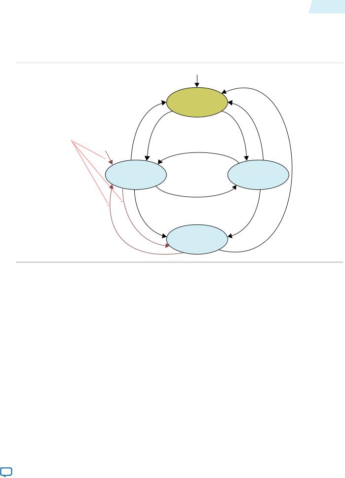
Remote System Upgrade Flow
Both the application configuration images, image 0 and image 1, are stored in the CFM. The MAX 10 device loads either one of the application configuration image from the CFM.
Figure 2-3: Remote System Upgrade Flow for MAX 10 Devices
Power-up
Flow when Auto-reconfigure from secondary image when initial image fails is disabled.
Reconfiguration
Sample CONFIG_SEL pin
Reconfiguration
CONFIG_SEL=0 CONFIG_SEL=1
Power-up
|
First Error Occurs |
Image 0 |
Image 1 |
|
First Error Occurs |
Second Error Occurs |
Second Error Occurs |
Error
ReconfigurationOccurs
Wait for Reconfiguration
Reconfiguration
The remote system upgrade feature detects errors in the following sequence:
1.After power-up, the device samples the CONFIG_SEL pin to determine which application configuration image to load. The CONFIG_SEL pin setting can be overwritten by the input register of the remote system upgrade circuitry for the subsequent reconfiguration.
2.If an error occurs, the remote system upgrade feature reverts by loading the other application configu ration image. These errors cause the remote system upgrade feature to load another application configuration image:
•Internal CRC error
•User watchdog timer time-out
3.Once the revert configuration completes and the device is in user mode, you can use the remote system upgrade circuitry to query the cause of error and which application image failed.
4.If a second error occurs, the device waits for a reconfiguration source. If the Auto-restart configura tion after error is enabled, the device will reconfigure without waiting for any reconfiguration source.
5.Reconfiguration is triggered by the following actions:
•Driving the nSTATUS low externally.
•Driving the nCONFIG low externally.
•Driving RU_nCONFIG low.
MAX 10 FPGA Configuration Schemes and Features |
Altera Corporation |
|
|
Send Feedback

2-10 |
Remote System Upgrade Circuitry |
UG-M10CONFIG |
|
2015.05.04 |
|||
|
|
Remote System Upgrade Circuitry
Figure 2-4: Remote System Upgrade Circuitry
|
Status Register (SR) |
|
|
|
Internal Oscillator |
|
|
|
|
|
|
|
|
|
|
||
Previous |
Previous |
Current |
|
Control Register |
|
|
|
|
State |
State |
State |
|
Bit [38..0] |
|
|
|
|
Register 2 |
Register 1 |
Logic |
|
|
|
|
|
|
Bit[31..0] |
Bit[31..0] |
Bit[33..0] |
|
|
|
|
|
|
|
|
|
|
Logic |
|
|
|
|
|
|
|
|
Input Register |
|
|
|
|
|
|
|
|
Bit [38..0] |
update |
|
|
|
|
|
|
|
|
|
RU |
|
|
|
|
|
|
|
|
Master |
|
|
|
|
|
|
|
|
State |
|
|
|
|
Logic |
|
|
|
Machine |
|
|
|
|
Shift Register |
|
|
|
RU |
timeout |
User |
|
|
|
|
|
Reconfiguration |
|||
|
din |
dout |
din |
|
dout |
State |
|
Watchdog |
|
|
Machine |
|
Timer |
||||
|
|
Bit [40..39] |
|
Bit [38..0] |
capture |
|
||
|
|
|
|
|
|
|||
|
|
|
|
|
|
|
|
|
|
|
|
|
clkout |
capture |
update |
|
|
|
|
|
|
|
Logic |
clkin |
|
|
RU_DIN |
RU_SHIFTnLD |
RU_CAPTnUPDT |
RU_CLK |
RU_DOUT |
RU_nCONFIG |
RU_nRSTIMER |
Logic Array
The remote system upgrade circuitry does the following functions:
•Tracks the current state of configuration
•Monitors all reconfiguration sources
•Provides access to set up the application configuration image
•Returns the device to fallback configuration if an error occurs
•Provides access to the information on the failed application configuration image
Remote System Upgrade Circuitry Signals
Table 2-6: Remote System Upgrade Circuitry Signals for MAX 10 Devices
Core Signal Name |
|
Logical |
|
Input/ |
|
Description |
|
|
Signal |
|
Output |
|
|
|
|
Name |
|
|
|
|
|
|
|
|
|
|
|
|
|
|
Use this signal to write data to the shift register on the rising |
RU_DIN |
regin |
Input |
edge of RU_CLK. To load data to the shift register, assert RU_ |
|
|
|
SHIFTnLD. |
|
|
|
|
Altera Corporation |
MAX 10 FPGA Configuration Schemes and Features |
|
|
Send Feedback

UG-M10CONFIG |
|
|
|
|
|
Remote System Upgrade Circuitry Input Control |
2-11 |
|
2015.05.04 |
|
|
|
|
|
|||
|
|
|
|
|
|
|
||
|
|
|
|
|
|
|
|
|
|
Core Signal Name |
|
Logical |
|
Input/ |
|
Description |
|
|
|
|
Signal |
|
Output |
|
|
|
|
|
|
Name |
|
|
|
|
|
|
|
|
|
|
|
|
|
|
|
|
|
|
|
|
|
Use this signal to get output data from the shift register. Data |
|
|
RU_DOUT |
|
regout |
|
Output |
|
is clocked out on each rising edge of RU_CLK if RU_SHIFTnLD is |
|
|
|
|
|
|
|
|
asserted. |
|
|
|
|
|
|
|
|
|
|
|
RU_nRSTIMER |
|
rsttimer |
|
Input |
|
Use this signal to reset the user watchdog timer. A falling edge |
|
|
|
|
|
of this signal triggers a reset of the user watchdog timer. |
|
|||
|
|
|
|
|
|
|
|
|
|
|
|
|
|
|
|
|
|
|
|
|
|
|
|
|
Use this signal to reconfigure the device. Driving this signal |
|
|
RU_nCONFIG |
|
rconfig |
|
Input |
|
low triggers the device to reconfigure if you enable the remote |
|
|
|
|
|
|
|
|
system upgrade feature. |
|
|
|
|
|
|
|
|
|
|
|
|
|
|
|
|
|
The clock to the remote system upgrade circuitry. All registers |
|
|
RU_CLK |
|
clk |
|
Input |
|
in this clock domain are enabled in user mode if you enable |
|
|
|
|
|
the remote system upgrade. Shift register and input register |
|
|||
|
|
|
|
|
|
|
|
|
|
|
|
|
|
|
|
are positive edge flip-flops. |
|
|
|
|
|
|
|
|
|
|
|
RU_SHIFTnLD |
|
shiftnld |
|
Input |
|
Control signals that determine the mode of remote system |
|
|
|
|
|
|
|
|
upgrade circuitry. |
|
|
|
|
|
|
|
|
|
|
|
|
|
|
|
|
|
• When RU_SHIFTnLD is driven low and RU_CAPTnUPDT is |
|
|
|
|
|
|
|
|
driven low, the input register is loaded with the contents of |
|
|
|
|
|
|
|
|
the shift register on the rising edge of RU_CLK. |
|
|
RU_CAPTnUPDT |
|
captnupdt |
|
Input |
|
• When RU_SHIFTnLD is driven low and RU_CAPTnUPDT is |
|
|
|
|
|
driven high, the shift register captures values from the |
|
|||
|
|
|
|
|
|
|||
|
|
|
|
|
|
|
input_cs_ps module on the rising edge of RU_CLK. |
|
|
|
|
|
|
|
|
• When RU_SHIFTnLD is driven high, the RU_CAPTnUPDT will |
|
|
|
|
|
|
|
|
be ignored and the shift register shifts data on each rising |
|
|
|
|
|
|
|
|
edge of RU_CLK. |
|
|
|
|
|
|
|
|
|
|
Related Information
•Accessing the Remote System Upgrade Block Through User Interface on page 3-8
Provides more information about accessing the remote system upgrade through user interface atom.
•MAX 10 Device Datasheet
Provides more information about Remote System Upgrade timing specifications.
Remote System Upgrade Circuitry Input Control
The remote system upgrade circuitry has three modes of operation.
•Update—loads the values in the shift register into the input register.
•Capture—loads the shift register with data to be shifted out.
•Shift—shifts out data to the user logic.
MAX 10 FPGA Configuration Schemes and Features |
Altera Corporation |
|
|
Send Feedback

2-12 |
Remote System Upgrade Input Register |
|
|
|
|
|
|
|
UG-M10CONFIG |
||||||
|
|
|
|
|
|
2015.05.04 |
|||||||||
|
|
|
|
|
|
|
|
|
|
|
|
|
|||
|
Table 2-7: Control Inputs to the Remote System Upgrade Circuitry |
|
|
|
|
|
|||||||||
|
|
|
|
|
|
|
|
|
|
|
|
|
|
|
|
|
|
Remote System Upgrade Circuitry Control Inputs |
|
Operation |
|
Input Settings for Registers |
|
||||||||
|
|
|
|
|
|
|
|
|
|
|
|
|
|
|
|
|
RU_SHIFTnLD |
|
RU_CAPTnUPDT |
|
Shift register |
|
Shift register |
|
|
Shift |
|
Input |
|
||
|
|
|
|
|
Mode |
|
|
|
|||||||
|
|
|
|
|
|
[40] |
|
[39] |
|
|
|
Register[38:0] |
|
Register[38:0] |
|
|
|
0 |
|
0 |
|
Don't Care |
|
Don't Care |
|
Update |
|
Shift Register |
|
Shift Register |
|
|
|
|
|
|
|
|
[38:0] |
|
[38:0] |
|
|||||
|
|
|
|
|
|
|
|
|
|
|
|
|
|
||
|
|
|
|
|
|
|
|
|
|
|
|
|
|
|
|
|
|
0 |
|
1 |
|
0 |
|
0 |
|
Capture |
|
Current State |
|
Input |
|
|
|
|
|
|
|
|
|
Register[38:0] |
|
||||||
|
|
|
|
|
|
|
|
|
|
|
|
|
|
|
|
|
|
|
|
|
|
|
|
|
|
|
|
{8’b0, |
|
Input |
|
|
|
0 |
|
1 |
|
0 |
|
1 |
|
Capture |
|
Previous State |
|
||
|
|
|
|
|
|
|
|
Register[38:0] |
|||||||
|
|
|
|
|
|
|
|
|
|
|
|
Application1} |
|
|
|
|
|
|
|
|
|
|
|
|
|
|
|
{8’b0, |
|
Input |
|
|
|
0 |
|
1 |
|
1 |
|
0 |
|
Capture |
|
Previous State |
|
|
|
|
|
|
|
|
|
|
|
Register[38:0] |
|
||||||
|
|
|
|
|
|
|
|
|
|
|
|
Application2} |
|
|
|
|
|
0 |
|
1 |
|
1 |
|
1 |
|
Capture |
|
Input |
|
Input |
|
|
|
|
|
|
|
|
Register[38:0] |
|
Register[38:0] |
||||||
|
|
|
|
|
|
|
|
|
|
|
|
|
|||
|
|
|
|
|
|
|
|
|
|
|
|
|
|
|
|
|
|
|
|
|
|
|
|
|
|
|
|
{ru_din, Shift |
|
Input |
|
|
|
1 |
|
Don't Care |
|
Don't Care |
|
Don't Care |
|
Shift |
|
Register |
|
|
|
|
|
|
|
|
|
|
|
Register[38:0] |
|
||||||
|
|
|
|
|
|
|
|
|
|
|
|
[38:1]} |
|
|
|
|
|
|
|
|
|
|
|
|
|
|
|
|
|
|
|
|
|
|
|
|
|
|
|
|
|
|
|
|
|
|
|
The following shows examples of driving the control inputs in the remote system upgrade circuitry:
•When you drive RU_SHIFTnLD high to 1’b1, the shift register shifts data on each rising edge of RU_CLK and RU_CAPTnUPDT has no function.
•When you drive both RU_SHIFTnLD and RU_CAPTnUPDT low to 1’b0, the input register is loaded with the contents of the shift register on the rising edge of RU_CLK.
•When you drive RU_SHIFTnLD low to 1’b0 and RU_CAPTnUPDT high to 1’b1, the shift register captures values on the rising edge of RU_DCLK.
Remote System Upgrade Input Register
Table 2-8: Remote System Upgrade Input Register for MAX 10 Devices
|
Bits |
|
Name |
|
Description |
|
|
|
|
|
|
|
|
|
|
38:14 |
|
|
Reserved |
|
Reserved—set to 0. |
||
|
|
|
|
|
|
|
|
|
|
|
|
|
|
• 0: Load configuration image 0 |
|
|
13 |
|
|
ru_config_sel |
|
• 1: Load configuration image 1 |
|
|
|
|
|
This bit will only work if the ru_config_sel_overwrite bit is set |
|
||
|
|
|
|
|
|
|
|
|
|
|
|
|
|
to 1. |
|
|
|
|
|
|
|
|
|
12 |
|
|
ru_config_sel_ |
|
• 0: Disable overwrite CONFIG_SEL pin |
||
|
|
overwrite |
|
• 1: Enable overwrite CONFIG_SEL pin |
|||
|
|
|
|
|
|||
|
|
|
|
|
|
|
|
|
|
|
|
|
|||
Altera Corporation |
|
|
|
|
MAX 10 FPGA Configuration Schemes and Features |
||
|
|
|
|
|
|
Send Feedback |
|

UG-M10CONFIG |
|
|
|
Remote System Upgrade Status Registers |
2-13 |
|
2015.05.04 |
|
|
|
|||
|
|
|
|
|
||
|
|
|
|
|
|
|
|
Bits |
|
Name |
|
Description |
|
|
|
|
|
|
|
|
|
11:0 |
|
Reserved |
|
Reserved—set to 0. |
|
|
|
|
|
|
|
|
Remote System Upgrade Status Registers
Table 2-9: Remote System Upgrade Status Register—Current State Logic Bit for MAX 10 Devices
Bits |
|
Name |
|
Description |
|
|
|
|
|
33:30 |
|
msm_cs |
|
The current state of the master state machine (MSM). |
|
|
|
|
|
29 |
|
ru_wd_en |
|
The current state of the enabled user watchdog timer. The default |
|
|
state is active high. |
||
|
|
|
|
|
28:0 |
|
wd_timeout_value |
|
The current, entire 29-bit watchdog time-out value. |
Table 2-10: Remote System Upgrade Status Register—Previous State Bit for MAX 10 Devices |
||||
|
|
|
|
|
Bits |
|
Name |
|
Description |
|
|
|
|
|
31 |
|
nconfig |
|
An active high field that describes the reconfiguration sources |
|
|
|
|
which caused the MAX 10 device to leave the previous application |
30 |
|
crcerror |
|
|
|
|
configuration. In the event of a tie, the higher bit order takes |
||
|
|
|
|
|
29 |
|
nstatus |
|
precedence. For example, if the nconfig and the ru_nconfig |
|
|
|
|
triggered at the same time, the nconfig takes precedence over the |
28 |
|
|
|
|
|
wdtimer |
|
ru_nconfig. |
|
|
|
|
|
|
27:26 |
|
Reserved |
|
Reserved—set to 0. |
|
|
|
|
|
|
|
|
|
The state of the MSM when a reconfiguration event occurred. The |
25:22 |
|
msm_cs |
|
reconfiguration will cause the device to leave the previous applica |
|
|
|
|
tion configuration. |
|
|
|
|
|
21:0 |
|
Reserved |
|
Reserved—set to 0. |
|
|
|
|
|
Master State Machine
The master state machine (MSM) tracks current configuration mode and enables the user watchdog timer.
Table 2-11: Remote System Upgrade Master State Machine Current State Descriptions for MAX 10 Devices
msm_cs Values |
|
State Description |
|
|
|
0010 |
|
Image 0 is being loaded. |
|
|
|
0011 |
|
Image 1 is being loaded after a revert in application image happens. |
|
|
|
0100 |
|
Image 1 is being loaded. |
|
|
|
0101 |
|
Image 0 is being loaded after a revert in application image happens. |
|
|
|
MAX 10 FPGA Configuration Schemes and Features |
Altera Corporation |
|
|
Send Feedback
Loading...