


CII51002-3.1
2. CycloneII Architecture
Functional Description
Cyclone®II devices contain a two-dimensional row- and column-based
architecture to implement custom logic. Column and row interconnects
of varying speeds provide signal interconnects between logic array
blocks (LABs), embedded memory blocks, and embedded multipliers.
The logic array consists of LABs, with 16 logic elements (LEs) in each
LAB. An LE is a small unit of logic providing efficient implementation of
user logic functions. LABs are grouped into rows and columns across the
device. Cyclone II devices range in density from 4,608 to 68,416 LEs.
Cyclone II devices provide a global clock network and up to four
phase-locked loops (PLLs). The global clock network consists of up to 16
global clock lines that drive throughout the entire device. The global clock
network can provide clocks for all resources within the device, such as
input/output elements (IOEs), LEs, embedded multipliers, and
embedded memory blocks. The global clock lines can also be used for
other high fan-out signals. Cyclone II PLLs provide general-purpose
clocking with clock synthesis and phase shifting as well as external
outputs for high-speed differential I/O support.
M4K memory blocks are true dual-port memory blocks with 4K bits of
memory plus parity (4,608 bits). These blocks provide dedicated true
dual-port, simple dual-port, or single-port memory up to 36-bits wide at
up to 260 MHz. These blocks are arranged in columns across the device
in between certain LABs. Cyclone II devices offer between 119 to
1,152 Kbits of embedded memory.
Each embedded multiplier block can implement up to either two 9 × 9-bit
multipliers, or one 18 × 18-bit multiplier with up to 250-MHz
performance. Embedded multipliers are arranged in columns across the
device.
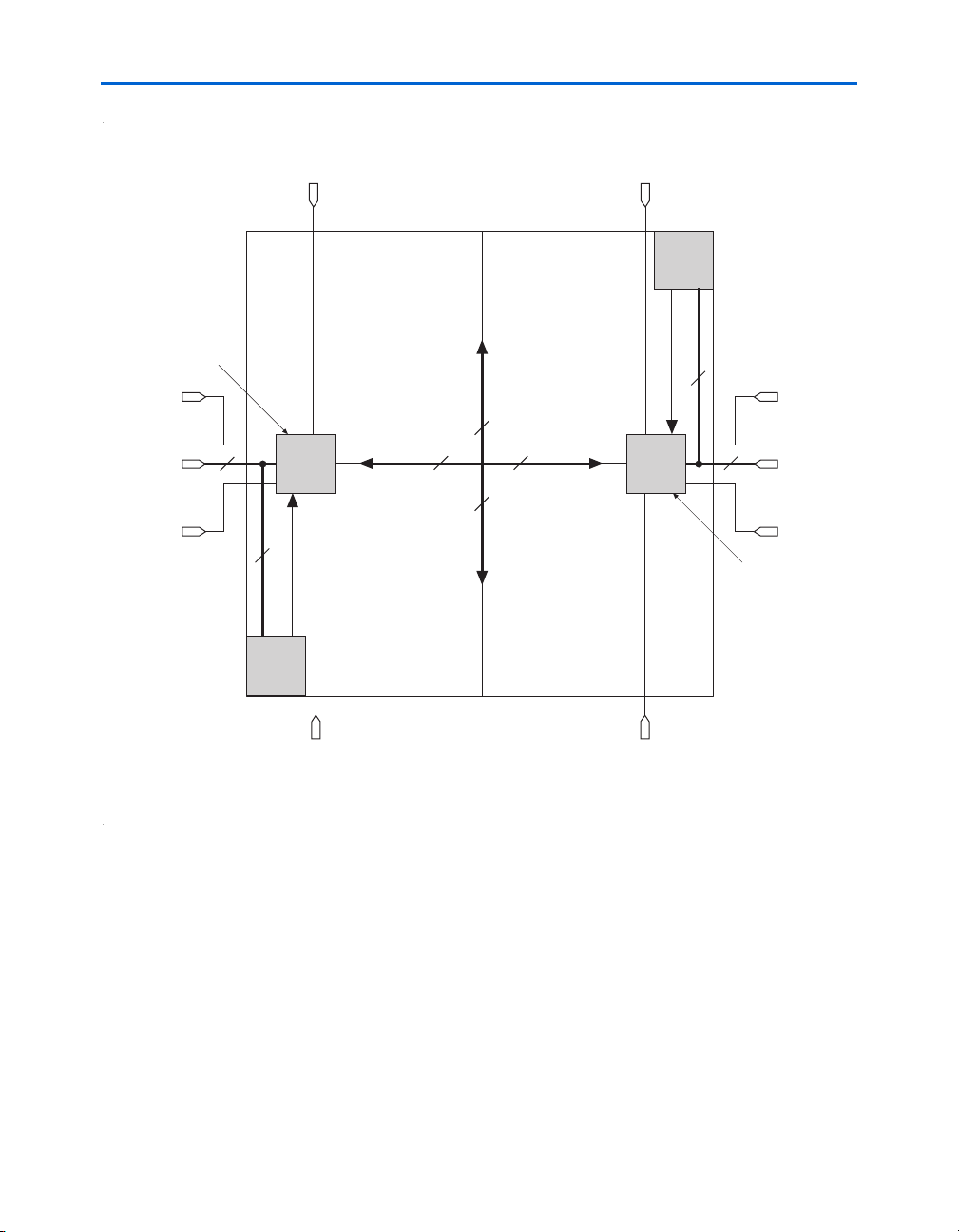
Each Cyclone II device I/O pin is fed by an IOE located at the ends of LAB
rows and columns around the periphery of the device. I/O pins support
various single-ended and differential I/O standards, such as the 66- and
33-MHz, 64- and 32-bit PCI standard, PCI-X, and the LVDS I/O standard
at a maximum data rate of 805 megabits per second (Mbps) for inputs and
640 Mbps for outputs. Each IOE contains a bidirectional I/O buffer and
three registers for registering input, output, and output-enable signals.
Dual-purpose DQS, DQ, and DM pins along with delay chains (used to
Altera Corporation 2–1
February 2007
Logic Elements
s
phase-align double data rate (DDR) signals) provide interface support for
external memory devices such as DDR, DDR2, and single data rate (SDR)
SDRAM, and QDRII SRAM devices at up to 167 MHz.
Figure 2–1 shows a diagram of the Cyclone II EP2C20 device.
Figure 2–1. Cyclone II EP2C20 Device Block Diagram
PLL PLLIOEs
Embedded
Multipliers
M4K Blocks
Logic Elements
Logic
IOEs
Array
PLL PLLIOEs
Logic
Array
Logic
Array
Logic
Array
IOEs
M4K Block
The number of M4K memory blocks, embedded multiplier blocks, PLLs,
rows, and columns vary per device.
The smallest unit of logic in the Cyclone II architecture, the LE, is compact
and provides advanced features with efficient logic utilization. Each LE
features:
■ A four-input look-up table (LUT), which is a function generator that
can implement any function of four variables
■ A programmable register
■ A carry chain connection
■ A register chain connection
■ The ability to drive all types of interconnects: local, row, column,
register chain, and direct link interconnects
■ Support for register packing
■ Support for register feedback
2–2 Altera Corporation
Cyclone II Device Handbook, Volume 1 February 2007
Figure 2–2. Cyclone II LE
y
LAB Carry-In
Figure 2–2 shows a Cyclone II LE.
Register Chain
Routing From
Previous LE
LAB-Wide
Synchronous
Load
Synchronous
LAB-Wide
Clear
Register Bypass
Packed
Register Select
Cyclone II Architecture
Programmable
Register
data1
data2
data3
data4
labclr1
labclr2
Chip-Wide
Reset
(DEV_CLRn)
labclk1
labclk2
labclkena1
labclkena2
Asynchronous
Clear Logic
Clock &
Clock Enable
Select
Look-Up
Ta bl e
(LUT)
Carry
Chain
LAB Carr
Synchronous
Load and
Clear Logic
-Out
D
ENA
CLRN
Register
Feedback
Q
Row, Column,
And Direct Link
Routing
Row, Column,
And Direct Link
Routing
Local Routing
Register Chain
Output
Each LE’s programmable register can be configured for D, T, JK, or SR
operation. Each register has data, clock, clock enable, and clear inputs.
Signals that use the global clock network, general-purpose I/O pins, or
any internal logic can drive the register’s clock and clear control signals.
Either general-purpose I/O pins or internal logic can drive the clock
enable. For combinational functions, the LUT output bypasses the
register and drives directly to the LE outputs.
Each LE has three outputs that drive the local, row, and column routing
resources. The LUT or register output can drive these three outputs
independently. Two LE outputs drive column or row and direct link
routing connections and one drives local interconnect resources, allowing
the LUT to drive one output while the register drives another output. This
feature, register packing, improves device utilization because the device
can use the register and the LUT for unrelated functions. When using
register packing, the LAB-wide synchronous load control signal is not
available. See “LAB Control Signals” on page 2–8 for more information.
Altera Corporation 2–3
February 2007 Cyclone II Device Handbook, Volume 1

Logic Elements
Another special packing mode allows the register output to feed back into
the LUT of the same LE so that the register is packed with its own fan-out
LUT, providing another mechanism for improved fitting. The LE can also
drive out registered and unregistered versions of the LUT output.
In addition to the three general routing outputs, the LEs within an LAB
have register chain outputs. Register chain outputs allow registers within
the same LAB to cascade together. The register chain output allows an
LAB to use LUTs for a single combinational function and the registers to
be used for an unrelated shift register implementation. These resources
speed up connections between LABs while saving local interconnect
resources. See “MultiTrack Interconnect” on page 2–10 for more
information on register chain connections.
LE Operating Modes
The Cyclone II LE operates in one of the following modes:
■ Normal mode
■ Arithmetic mode
Each mode uses LE resources differently. In each mode, six available
inputs to the LE—the four data inputs from the LAB local interconnect,
the LAB carry-in from the previous carry-chain LAB, and the register
chain connection—are directed to different destinations to implement the
desired logic function. LAB-wide signals provide clock, asynchronous
clear, synchronous clear, synchronous load, and clock enable control for
the register. These LAB-wide signals are available in all LE modes.
®
The Quartus
II software, in conjunction with parameterized functions
such as library of parameterized modules (LPM) functions, automatically
chooses the appropriate mode for common functions such as counters,
adders, subtractors, and arithmetic functions. If required, you can also
create special-purpose functions that specify which LE operating mode to
use for optimal performance.
Normal Mode
The normal mode is suitable for general logic applications and
combinational functions. In normal mode, four data inputs from the LAB
local interconnect are inputs to a four-input LUT (see Figure 2–3). The
Quartus II Compiler automatically selects the carry-in or the data3
signal as one of the inputs to the LUT. LEs in normal mode support
packed registers and register feedback.
2–4 Altera Corporation
Cyclone II Device Handbook, Volume 1 February 2007
Figure 2–3. LE in Normal Mode
Cyclone II Architecture
data1
data2
data3
cin (from cout
of previous LE)
data4
Packed Register Input
Four-Input
Register Feedback
Arithmetic Mode
The arithmetic mode is ideal for implementing adders, counters,
accumulators, and comparators. An LE in arithmetic mode implements a
2-bit full adder and basic carry chain (see Figure 2–4). LEs in arithmetic
mode can drive out registered and unregistered versions of the LUT
output. Register feedback and register packing are supported when LEs
are used in arithmetic mode.
Register chain
connection
LUT
sload
(LAB Wide)
clock (LAB Wide)
ena (LAB Wide)
aclr (LAB Wide)
(LAB Wide)
sclear
D
ENA
CLRN
Q
Row, Column, and
Direct Link Routing
Row, Column, and
Direct Link Routing
Local routing
Register
chain output
Altera Corporation 2–5
February 2007 Cyclone II Device Handbook, Volume 1
Logic Elements
Figure 2–4. LE in Arithmetic Mode
(LAB Wide)
Register chain
connection
sload
sclear
(LAB Wide)
data1
data2
cin (from cout
of previous LE)
Three-Input
LUT
Three-Input
LUT
clock (LAB Wide)
ena (LAB Wide)
aclr (LAB Wide)
cout
Register Feedback
D
ENA
Q
CLRN
Row, column, and
direct link routing
Row, column, and
direct link routing
Local routing
Register
chain output
The Quartus II Compiler automatically creates carry chain logic during
design processing, or you can create it manually during design entry.
Parameterized functions such as LPM functions automatically take
advantage of carry chains for the appropriate functions.
The Quartus II Compiler creates carry chains longer than 16 LEs by
automatically linking LABs in the same column. For enhanced fitting, a
long carry chain runs vertically, which allows fast horizontal connections
to M4K memory blocks or embedded multipliers through direct link
interconnects. For example, if a design has a long carry chain in a LAB
column next to a column of M4K memory blocks, any LE output can feed
an adjacent M4K memory block through the direct link interconnect.
Whereas if the carry chains ran horizontally, any LAB not next to the
column of M4K memory blocks would use other row or column
interconnects to drive a M4K memory block. A carry chain continues as
far as a full column.
2–6 Altera Corporation
Cyclone II Device Handbook, Volume 1 February 2007
Cyclone II Architecture
t
Logic Array Blocks
Each LAB consists of the following:
■ 16 LEs
■ LAB control signals
■ LE carry chains
■ Register chains
■ Local interconnect
The local interconnect transfers signals between LEs in the same LAB.
Register chain connections transfer the output of one LE’s register to the
adjacent LE’s register within an LAB. The Quartus II Compiler places
associated logic within an LAB or adjacent LABs, allowing the use of
local, and register chain connections for performance and area efficiency.
Figure 2–5 shows the Cyclone II LAB.
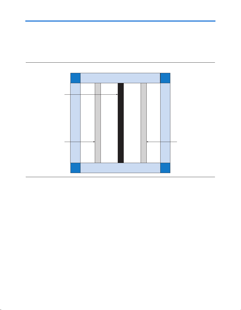
Figure 2–5. Cyclone II LAB Structure
Row Interconnect
Column
Interconnect
Direct link
Direct link
interconnect
from adjacent
block
Direct link
interconnect
to adjacent
block
LAB
Local Interconnect
interconnect
from adjacen
block
Direct link
interconnect
to adjacent
block
Altera Corporation 2–7
February 2007 Cyclone II Device Handbook, Volume 1
Logic Array Blocks
LAB Interconnects
The LAB local interconnect can drive LEs within the same LAB. The LAB
local interconnect is driven by column and row interconnects and LE
outputs within the same LAB. Neighboring LABs, PLLs, M4K RAM
blocks, and embedded multipliers from the left and right can also drive
an LAB’s local interconnect through the direct link connection. The direct
link connection feature minimizes the use of row and column
interconnects, providing higher performance and flexibility. Each LE can
drive 48 LEs through fast local and direct link interconnects. Figure 2–6
shows the direct link connection.
Figure 2–6. Direct Link Connection
Direct link interconnect from
left LAB, M4K memory
block, embedded multiplier,
PLL, or IOE output
Direct link
interconnect
to left
Interconnect
Direct link interconnect from
right LAB, M4K memory
block, embedded multiplier,
PLL, or IOE output
Direct link
interconnect
to right
Local
LAB
LAB Control Signals
Each LAB contains dedicated logic for driving control signals to its LEs.
The control signals include:
■ Two clocks
■ Two clock enables
■ Two asynchronous clears
■ One synchronous clear
■ One synchronous load
2–8 Altera Corporation
Cyclone II Device Handbook, Volume 1 February 2007
Cyclone II Architecture
This gives a maximum of seven control signals at a time. When using the
LAB-wide synchronous load, the clkena of labclk1 is not available.
Additionally, register packing and synchronous load cannot be used
simultaneously.
Each LAB can have up to four non-global control signals. Additional LAB
control signals can be used as long as they are global signals.
Synchronous clear and load signals are useful for implementing counters
and other functions. The synchronous clear and synchronous load signals
are LAB-wide signals that affect all registers in the LAB.
Each LAB can use two clocks and two clock enable signals. Each LAB’s
clock and clock enable signals are linked. For example, any LE in a
particular LAB using the labclk1 signal also uses labclkena1. If the
LAB uses both the rising and falling edges of a clock, it also uses both
LAB-wide clock signals. De-asserting the clock enable signal turns off the
LAB-wide clock.
The LAB row clocks [5..0] and LAB local interconnect generate the LABwide control signals. The MultiTrack
allows clock and control signal distribution in addition to data. Figure 2–7
shows the LAB control signal generation circuit.
Figure 2–7. LAB-Wide Control Signals
Dedicated
LAB Row
Clocks
Local
Interconnect
Local
Interconnect
Local
Interconnect
Local
Interconnect
6
LAB-wide signals control the logic for the register’s clear signal. The LE
directly supports an asynchronous clear function. Each LAB supports up
to two asynchronous clear signals (labclr1 and labclr2).
labclkena1
™
interconnect’s inherent low skew
labclkena2
labclk2labclk1
syncload
labclr1
labclr2
synclr
Altera Corporation 2–9
February 2007 Cyclone II Device Handbook, Volume 1

MultiTrack Interconnect
A LAB-wide asynchronous load signal to control the logic for the
register’s preset signal is not available. The register preset is achieved by
using a NOT gate push-back technique. Cyclone II devices can only
support either a preset or asynchronous clear signal.
In addition to the clear port, Cyclone II devices provide a chip-wide reset
pin (DEV_CLRn) that resets all registers in the device. An option set before
compilation in the Quartus II software controls this pin. This chip-wide
reset overrides all other control signals.
MultiTrack
Interconnect
In the Cyclone II architecture, connections between LEs, M4K memory
blocks, embedded multipliers, and device I/O pins are provided by the
MultiTrack interconnect structure with DirectDrive™ technology. The
MultiTrack interconnect consists of continuous, performance-optimized
routing lines of different speeds used for inter- and intra-design block
connectivity. The Quartus II Compiler automatically places critical paths
on faster interconnects to improve design performance.
DirectDrive technology is a deterministic routing technology that ensures
identical routing resource usage for any function regardless of placement
within the device. The MultiTrack interconnect and DirectDrive
technology simplify the integration stage of block-based designing by
eliminating the re-optimization cycles that typically follow design
changes and additions.
The MultiTrack interconnect consists of row (direct link, R4, and R24) and
column (register chain, C4, and C16) interconnects that span fixed
distances. A routing structure with fixed-length resources for all devices
allows predictable and repeatable performance when migrating through
different device densities.
Row Interconnects
Dedicated row interconnects route signals to and from LABs, PLLs, M4K
memory blocks, and embedded multipliers within the same row. These
row resources include:
■ Direct link interconnects between LABs and adjacent blocks
■ R4 interconnects traversing four blocks to the right or left
■ R24 interconnects for high-speed access across the length of the
device
2–10 Altera Corporation
Cyclone II Device Handbook, Volume 1 February 2007
Cyclone II Architecture
The direct link interconnect allows an LAB, M4K memory block, or
embedded multiplier block to drive into the local interconnect of its left
and right neighbors. Only one side of a PLL block interfaces with direct
link and row interconnects. The direct link interconnect provides fast
communication between adjacent LABs and/or blocks without using
row interconnect resources.
The R4 interconnects span four LABs, three LABs and one M4K memory
block, or three LABs and one embedded multiplier to the right or left of a
source LAB. These resources are used for fast row connections in a fourLAB region. Every LAB has its own set of R4 interconnects to drive either
left or right. Figure 2–8 shows R4 interconnect connections from an LAB.
R4 interconnects can drive and be driven by LABs, M4K memory blocks,
embedded multipliers, PLLs, and row IOEs. For LAB interfacing, a
primary LAB or LAB neighbor (see Figure 2–8) can drive a given R4
interconnect. For R4 interconnects that drive to the right, the primary
LAB and right neighbor can drive on to the interconnect. For R4
interconnects that drive to the left, the primary LAB and its left neighbor
can drive on to the interconnect. R4 interconnects can drive other R4
interconnects to extend the range of LABs they can drive. Additionally,
R4 interconnects can drive R24 interconnects, C4, and C16 interconnects
for connections from one row to another.
Figure 2–8. R4 Interconnect Connections
Adjacent LAB can
R4 Interconnect
Driving Left
Drive onto Another
LAB's R4 Interconnect
LAB
Neighbor
Primary
LAB (2)
C4 Column Interconnects (1)
LAB
Neighbor
Notes to Figure 2–8:
(1) C4 interconnects can drive R4 interconnects.
(2) This pattern is repeated for every LAB in the LAB row.
Altera Corporation 2–11
February 2007 Cyclone II Device Handbook, Volume 1
R4 Interconnect
Driving Right

MultiTrack Interconnect
R24 row interconnects span 24 LABs and provide the fastest resource for
long row connections between non-adjacent LABs, M4K memory blocks,
dedicated multipliers, and row IOEs. R24 row interconnects drive to
other row or column interconnects at every fourth LAB. R24 row
interconnects drive LAB local interconnects via R4 and C4 interconnects
and do not drive directly to LAB local interconnects. R24 interconnects
can drive R24, R4, C16, and C4 interconnects.
Column Interconnects
The column interconnect operates similar to the row interconnect. Each
column of LABs is served by a dedicated column interconnect, which
vertically routes signals to and from LABs, M4K memory blocks,
embedded multipliers, and row and column IOEs. These column
resources include:
■ Register chain interconnects within an LAB
■ C4 interconnects traversing a distance of four blocks in an up and
down direction
■ C16 interconnects for high-speed vertical routing through the device
Cyclone II devices include an enhanced interconnect structure within
LABs for routing LE output to LE input connections faster using register
chain connections. The register chain connection allows the register
output of one LE to connect directly to the register input of the next LE in
the LAB for fast shift registers. The Quartus II Compiler automatically
takes advantage of these resources to improve utilization and
performance. Figure 2–9 shows the register chain interconnects.
2–12 Altera Corporation
Cyclone II Device Handbook, Volume 1 February 2007
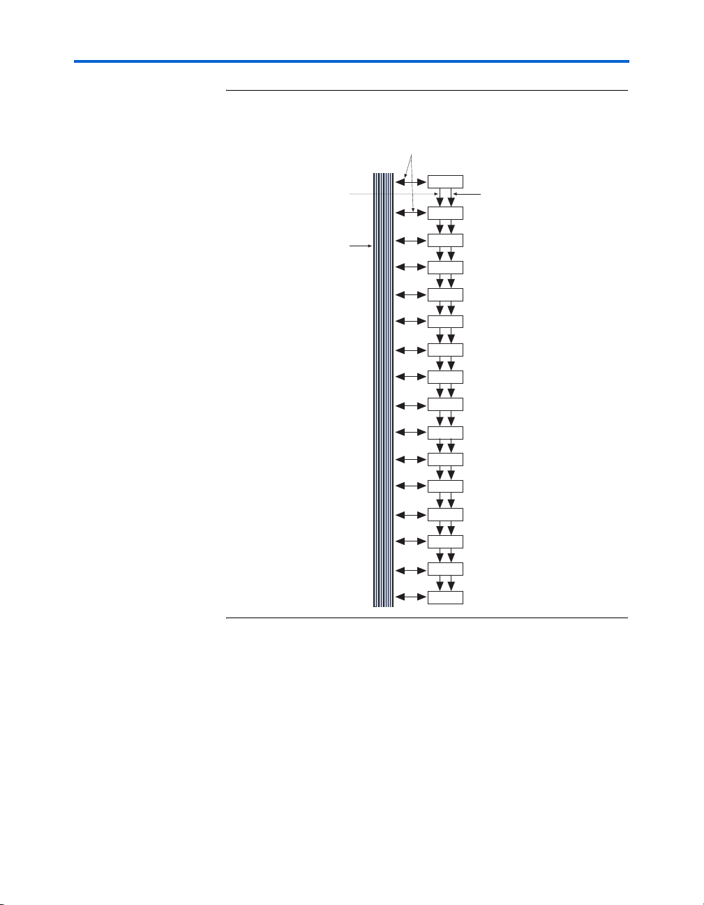
Figure 2–9. Register Chain Interconnects
t
Local Interconnect
Routing Among LEs
in the LAB
Cyclone II Architecture
Carry Chain
Routing to
Adjacent LE
Local
Interconnect
LE 1
LE 2
LE 3
LE 4
LE 5
LE 6
LE 7
LE 8
LE 9
LE 10
LE 11
LE 12
LE13
LE 14
LE 15
Register Chain
Routing to Adjacen
LE's Register Input
LE 16
The C4 interconnects span four LABs, M4K blocks, or embedded
multipliers up or down from a source LAB. Every LAB has its own set of
C4 interconnects to drive either up or down. Figure 2–10 shows the C4
interconnect connections from an LAB in a column. The C4 interconnects
can drive and be driven by all types of architecture blocks, including
PLLs, M4K memory blocks, embedded multiplier blocks, and column
and row IOEs. For LAB interconnection, a primary LAB or its LAB
neighbor (see Figure 2–10) can drive a given C4 interconnect. C4
interconnects can drive each other to extend their range as well as drive
row interconnects for column-to-column connections.
Altera Corporation 2–13
February 2007 Cyclone II Device Handbook, Volume 1
MultiTrack Interconnect
4
Figure 2–10. C4 Interconnect Connections Note (1)
C4 Interconnect
Drives Local and R
Interconnects
Up to Four Rows
C4 Interconnect
Driving Up
LAB
Row
Interconnect
Adjacent LAB can
drive onto neighboring
LAB's C4 interconnect
Local
Interconnect
Primary
LAB
LAB
Neighbor
C4 Interconnect
Driving Down
Note to Figure 2–10:
(1) Each C4 interconnect can drive either up or down four rows.
2–14 Altera Corporation
Cyclone II Device Handbook, Volume 1 February 2007
C16 column interconnects span a length of 16 LABs and provide the
fastest resource for long column connections between LABs, M4K
memory blocks, embedded multipliers, and IOEs. C16 column
interconnects drive to other row and column interconnects at every
fourth LAB. C16 column interconnects drive LAB local interconnects via
C4 and R4 interconnects and do not drive LAB local interconnects
directly. C16 interconnects can drive R24, R4, C16, and C4 interconnects.
Device Routing
All embedded blocks communicate with the logic array similar to
LAB-to-LAB interfaces. Each block (for example, M4K memory,
embedded multiplier, or PLL) connects to row and column interconnects
and has local interconnect regions driven by row and column
interconnects. These blocks also have direct link interconnects for fast
connections to and from a neighboring LAB.
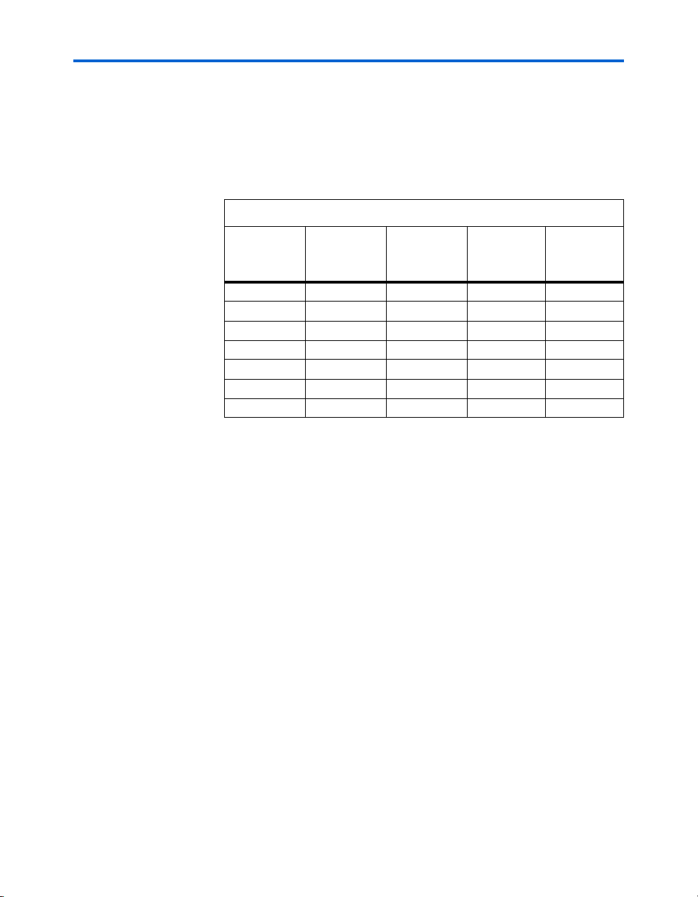
Table 2–1 shows the Cyclone II device’s routing scheme.
Table 2–1. Cyclone II Device Routing Scheme (Part 1 of 2)
Destination
Cyclone II Architecture
Source
LE
Register Chain
Local Interconnect
R4 Interconnect
C4 Interconnect
R24 Interconnect
C16 Interconnect
M4K RAM Block
Direct Link Interconnect
Register
Chain
Local
Interconnect
Direct Link
Interconnect
R4
Interconnect
R24
Interconnect
C4
Interconnect
C16
Interconnect
Altera Corporation 2–15
February 2007 Cyclone II Device Handbook, Volume 1
v
v vvvv
vvvv
v vvvv
vvvv
v
vvvvvv
PLL
Column IOE
Embedded Multiplier
Row IOE
Global Clock Network & Phase-Locked Loops
Table 2–1. Cyclone II Device Routing Scheme (Part 2 of 2)
Destination
Source
Register Chain
Local Interconnect
LE vvvv v
M4K memory
Block
Embedded
Multipliers
PLL vv v
Column IOE vv
Row IOE vvvv
vvv v
vvv v
R4 Interconnect
Direct Link Interconnect
C4 Interconnect
R24 Interconnect
C16 Interconnect
LE
M4K RAM Block
Embedded Multiplier
PLL
Row IOE
Column IOE
Global Clock
Network &
Phase-Locked
Loops
2–16 Altera Corporation
Cyclone II Device Handbook, Volume 1 February 2007
Cyclone II devices provide global clock networks and up to four PLLs for
a complete clock management solution. Cyclone II clock network features
include:
■ Up to 16 global clock networks
■ Up to four PLLs
■ Global clock network dynamic clock source selection
■ Global clock network dynamic enable and disable
Cyclone II Architecture
Each global clock network has a clock control block to select from a
number of input clock sources (PLL clock outputs, CLK[] pins, DPCLK[]
pins, and internal logic) to drive onto the global clock network. Tab le 2 –2
lists how many PLLs, CLK[] pins, DPCLK[] pins, and global clock
networks are available in each Cyclone II device. CLK[] pins are
dedicated clock pins and DPCLK[] pins are dual-purpose clock pins.
Table 2–2. Cyclone II Device Clock Resources
Device
EP2C5 2 8 8 8
EP2C8 2 8 8 8
EP2C15 4 16 20 16
EP2C20 4 16 20 16
EP2C35 4 16 20 16
EP2C50 4 16 20 16
EP2C70 4 16 20 16
Number of
PLLs
Number of
CLK Pins
Number of
DPCLK Pins
Number of
Global Clock
Networks
Figures 2–11 and 2–12 show the location of the Cyclone II PLLs, CLK[]
inputs, DPCLK[] pins, and clock control blocks.
Altera Corporation 2–17
February 2007 Cyclone II Device Handbook, Volume 1
Global Clock Network & Phase-Locked Loops
Figure 2–11. EP2C5 & EP2C8 PLL, CLK[], DPCLK[] & Clock Control Block Locations
DPCLK10 DPCLK8
Clock Control
Block (1)
PLL 2
DPCLK0
CLK[3..0]
DPCLK1
4
4
PLL 1
DPCLK2
GCLK[7..0]
Note to Figure 2–11:
(1) There are four clock control blocks on each side.
4
8
8
8
4
8
GCLK[7..0]
Clock Control
DPCLK4
DPCLK7
CLK[7..4]
DPCLK6
Block (1)
2–18 Altera Corporation
Cyclone II Device Handbook, Volume 1 February 2007
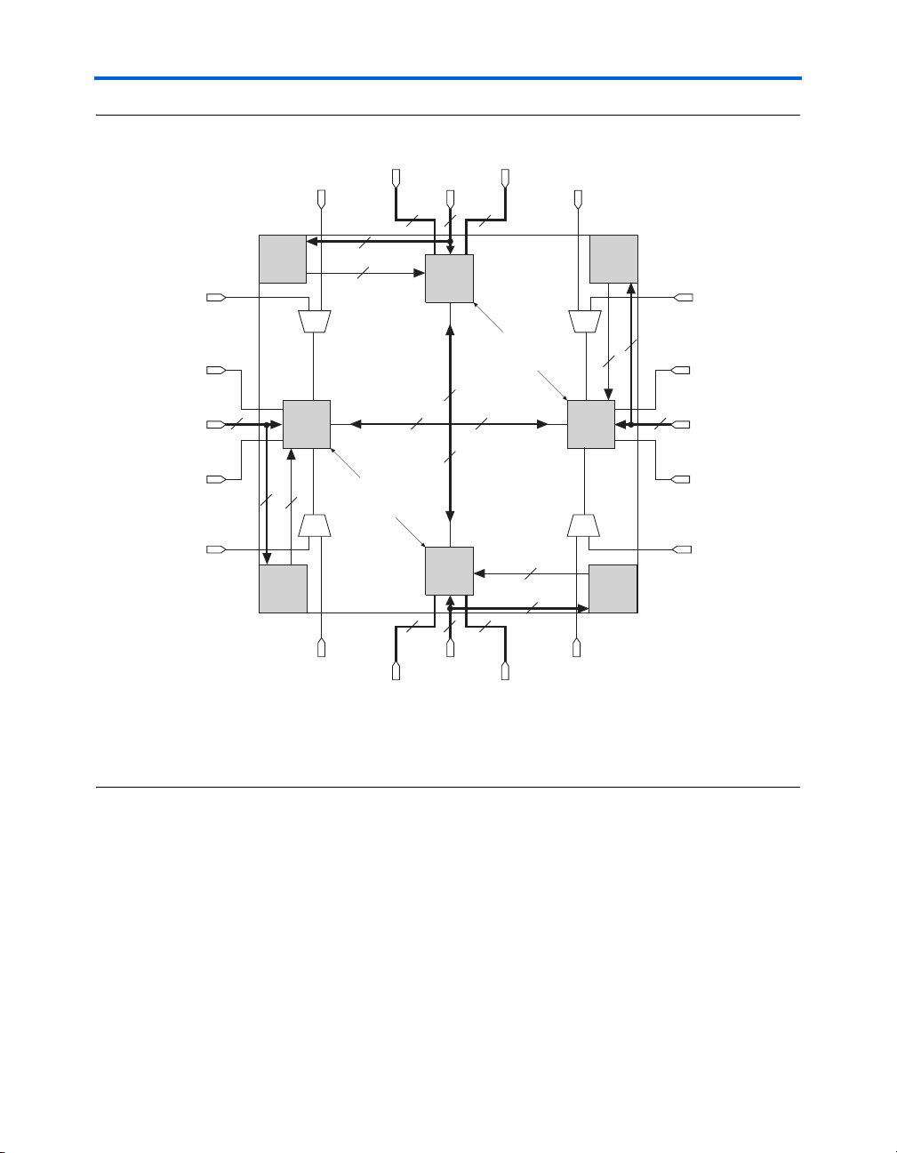
Figure 2–12. EP2C15 & Larger PLL, CLK[], DPCLK[] & Clock Control Block Locations
DPCLK[9..8]DPCLK[11..10]
CDPCLK7
CLK[11..8]
4
CDPCLK6
22
Cyclone II Architecture
4
3
GCLK[15..0]
Clock Control
Block (1)
Clock Control
Block (1)
16
16 16
16
GCLK[15..0]
3
4
4
22
CLK[15..12] CDPCLK3
DPCLK[5..4]DPCLK[3..2]
3
PLL 4
CDPCLK5
4
DPCLK7
CLK[7..4]
4
DPCLK6
CDPCLK4
CDPCLK0
DPCLK0
CLK[3..0]
DPCLK1
CDPCLK1
PLL 3 PLL 2
(2) (2)
4
4
3
(2) (2)
PLL 1
CDPCLK2
Notes to Figure 2–12:
(1) There are four clock control blocks on each side.
(2) Only one of the corner CDPCLK pins in each corner can feed the clock control block at a time. The other CDPCLK pins
can be used as general-purpose I/O pins.
Altera Corporation 2–19
February 2007 Cyclone II Device Handbook, Volume 1

Global Clock Network & Phase-Locked Loops
Dedicated Clock Pins
Larger Cyclone II devices (EP2C15 and larger devices) have 16 dedicated
clock pins (CLK[15..0], four pins on each side of the device). Smaller
Cyclone II devices (EP2C5 and EP2C8 devices) have eight dedicated clock
pins (CLK[7..0], four pins on left and right sides of the device). These
CLK pins drive the global clock network (GCLK), as shown in
Figures 2–11 and 2–12.
If the dedicated clock pins are not used to feed the global clock networks,
they can be used as general-purpose input pins to feed the logic array
using the MultiTrack interconnect. However, if they are used as generalpurpose input pins, they do not have support for an I/O register and
must use LE-based registers in place of an I/O register.
Dual-Purpose Clock Pins
Cyclone II devices have either 20 dual-purpose clock pins,
DPCLK[19..0] or 8 dual-purpose clock pins, DPCLK[7..0]. In the
larger Cyclone II devices (EP2C15 devices and higher), there are
20 DPCLK pins; four on the left and right sides and six on the top and
bottom of the device. The corner CDPCLK pins are first multiplexed before
they drive into the clock control block. Since the signals pass through a
multiplexer before feeding the clock control block, these signals incur
more delay to the clock control block than other DPCLK pins that directly
feed the clock control block. In the smaller Cyclone II devices (EP2C5 and
EP2C8 devices), there are eight DPCLK pins; two on each side of the device
(see Figures 2–11 and 2–12).
A programmable delay chain is available from the DPCLK pin to its fanout destinations. To set the propagation delay from the DPCLK pin to its
fan-out destinations, use the Input Delay from Dual-Purpose Clock Pin
to Fan-Out Destinations assignment in the Quartus II software.
These dual-purpose pins can connect to the global clock network for
high-fanout control signals such as clocks, asynchronous clears, presets,
and clock enables, or protocol control signals such as TRDY and IRDY for
PCI, or DQS signals for external memory interfaces.
2–20 Altera Corporation
Cyclone II Device Handbook, Volume 1 February 2007

Cyclone II Architecture
Global Clock Network
The 16 or 8 global clock networks drive throughout the entire device.
Dedicated clock pins (CLK[]), PLL outputs, the logic array, and
dual-purpose clock (DPCLK[]) pins can also drive the global clock
network.
The global clock network can provide clocks for all resources within the
device, such as IOEs, LEs, memory blocks, and embedded multipliers.
The global clock lines can also be used for control signals, such as clock
enables and synchronous or asynchronous clears fed from the external
pin, or DQS signals for DDR SDRAM or QDRII SRAM interfaces. Internal
logic can also drive the global clock network for internally generated
global clocks and asynchronous clears, clock enables, or other control
signals with large fan-out.
Clock Control Block
There is a clock control block for each global clock network available in
Cyclone II devices. The clock control blocks are arranged on the device
periphery and there are a maximum of 16 clock control blocks available
per Cyclone II device. The larger Cyclone II devices (EP2C15 devices and
larger) have 16 clock control blocks, four on each side of the device. The
smaller Cyclone II devices (EP2C5 and EP2C8 devices) have eight clock
control blocks, four on the left and right sides of the device.
The control block has these functions:
■ Dynamic global clock network clock source selection
■ Dynamic enable/disable of the global clock network
In Cyclone II devices, the dedicated CLK[] pins, PLL counter outputs,
DPCLK[] pins, and internal logic can all feed the clock control block. The
output from the clock control block in turn feeds the corresponding
global clock network.
The following sources can be inputs to a given clock control block:
■ Four clock pins on the same side as the clock control block
■ Three PLL clock outputs from a PLL
■ Four DPCLK pins (including CDPCLK pins) on the same side as the
clock control block
■ Four internally-generated signals
Altera Corporation 2–21
February 2007 Cyclone II Device Handbook, Volume 1

Global Clock Network & Phase-Locked Loops
Of the sources listed, only two clock pins, two PLL clock outputs, one
DPCLK pin, and one internally-generated signal are chosen to drive into a
clock control block. Figure 2–13 shows a more detailed diagram of the
clock control block. Out of these six inputs, the two clock input pins and
two PLL outputs can be dynamic selected to feed a global clock network.
The clock control block supports static selection of DPCLK and the signal
from internal logic.
Figure 2–13. Clock Control Block
Internal Logic
Static Clock Select (3)
DPCLK or
CDPCLK
Clock Control Block
Enable/
Disable
Global
Clock
Static Clock
Select (3)
CLK[n + 3]
CLK[n + 2]
CLK[n + 1]
CLK[n]
inclk1
inclk0
CLKSWITCH (1)
(3)
PLL
C0
C1
C2
CLKSELECT[1..0] (2) CLKENA (4)
f
IN
Notes to Figure 2–13:
(1) The CLKSWITCH signal can either be set through the configuration file or it can be dynamically set when using the
manual PLL switchover feature. The output of the multiplexer is the input reference clock (fIN) for the PLL.
(2) The CLKSELECT[1..0] signals are fed by internal logic and can be used to dynamically select the clock source for
the global clock network when the device is in user mode.
(3) The static clock select signals are set in the configuration file and cannot be dynamically controlled when the device
is in user mode.
(4) Internal logic can be used to enabled or disabled the global clock network in user mode.
2–22 Altera Corporation
Cyclone II Device Handbook, Volume 1 February 2007

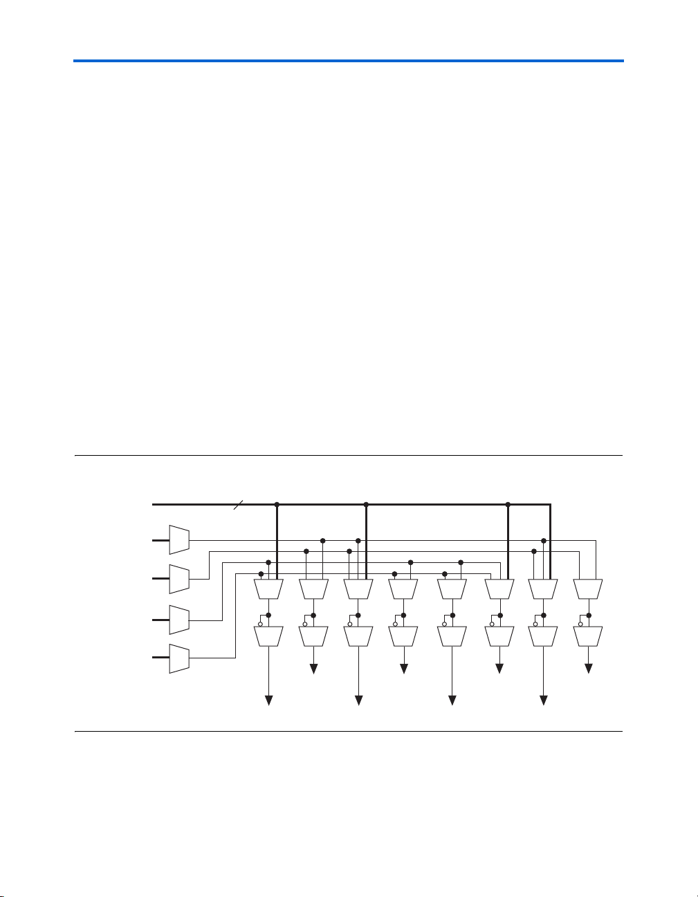
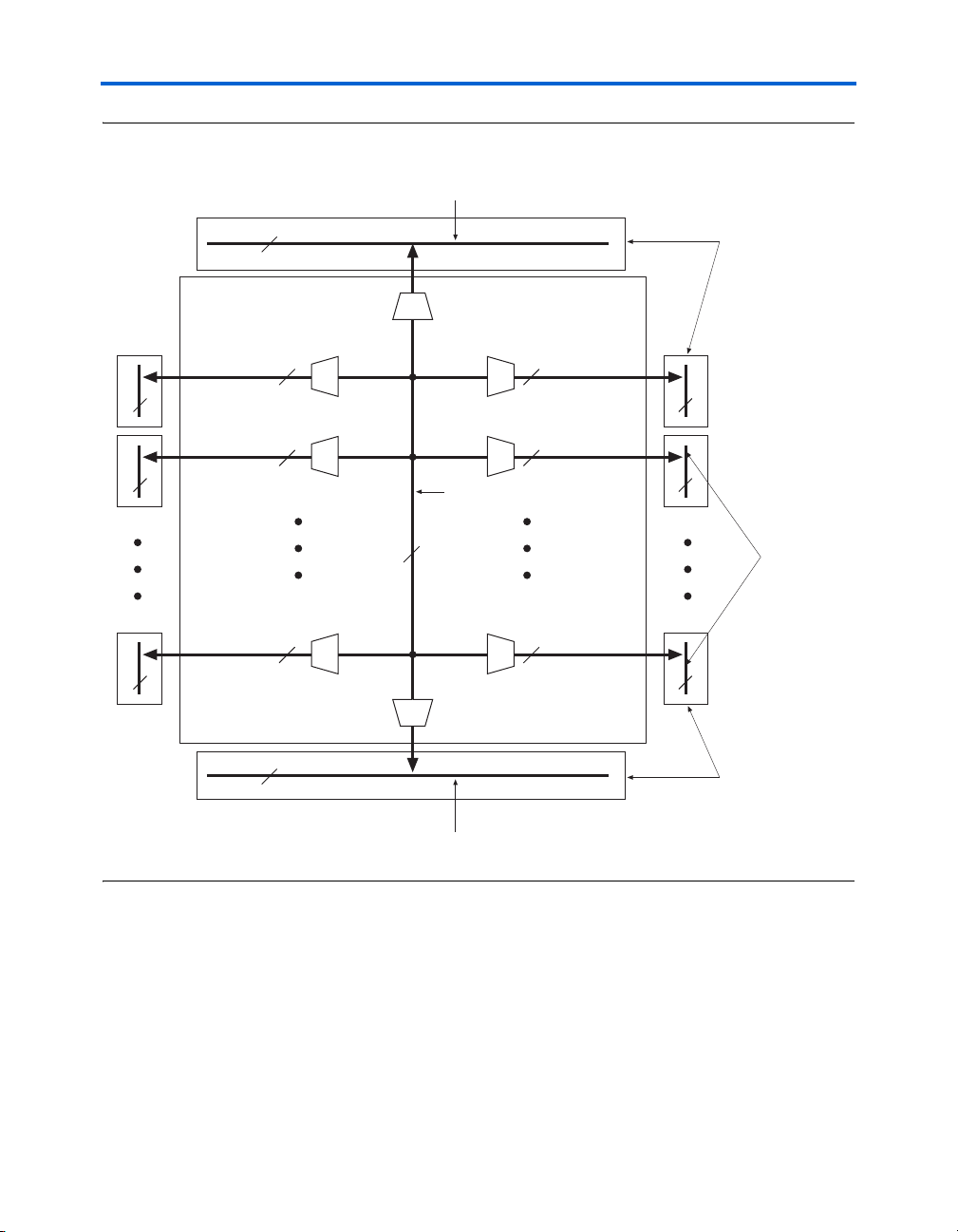
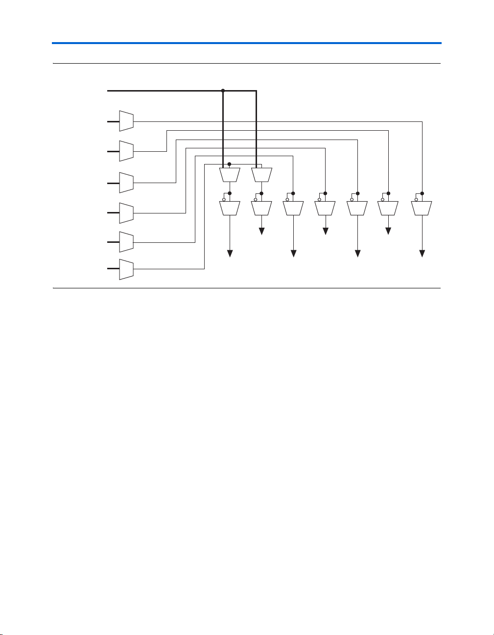
Global Clock Network Distribution
Cyclone II devices contains 16 global clock networks. The device uses
multiplexers with these clocks to form six-bit buses to drive column IOE
clocks, LAB row clocks, or row IOE clocks (see Figure 2–14). Another
multiplexer at the LAB level selects two of the six LAB row clocks to feed
the LE registers within the LAB.
Figure 2–14. Global Clock Network Multiplexers
Global Clock
Network
Cyclone II Architecture
Column I/O Region
IO_CLK [5..0]
Clock [15 or 7..0]
LAB Row Clock
LABCLK[5..0]
Row I/O Region
IO_CLK [5..0]
LAB row clocks can feed LEs, M4K memory blocks, and embedded
multipliers. The LAB row clocks also extend to the row I/O clock regions.
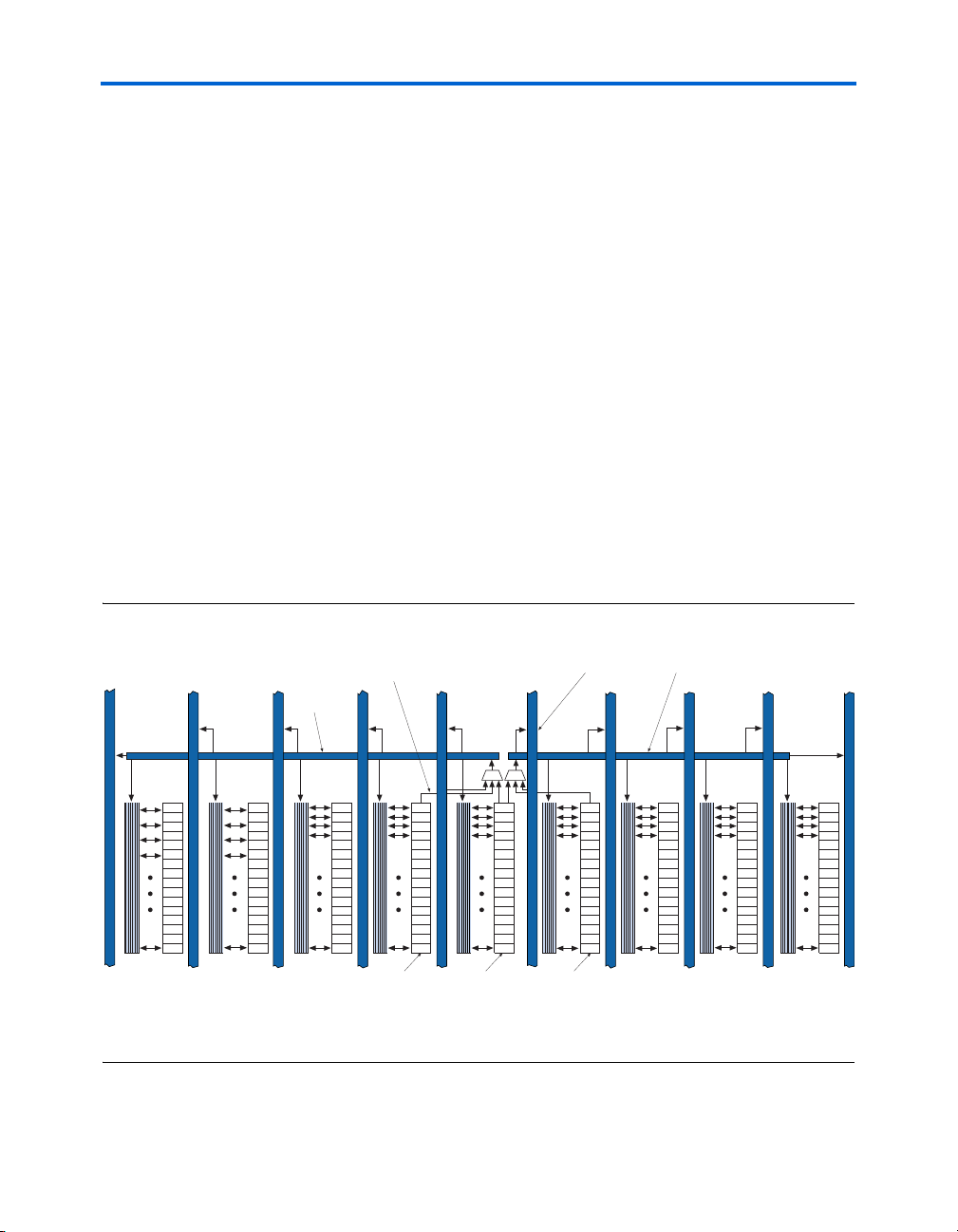
IOE clocks are associated with row or column block regions. Only six
global clock resources feed to these row and column regions. Figure 2–15
shows the I/O clock regions.
Altera Corporation 2–23
February 2007 Cyclone II Device Handbook, Volume 1
Global Clock Network & Phase-Locked Loops
k
Figure 2–15. LAB & I/O Clock Regions
Column I/O Clock Region
IO_CLK[5..0]
6
Cyclone Logic Array
LAB Row Clocks
labclk[5..0]
6
LAB Row Clocks
labclk[5..0]
6
LAB Row Clocks
labclk[5..0]
6
6 6
6
Global Clock
Network
8 or 16
6
6
LAB Row Clocks
labclk[5..0]
LAB Row Clocks
labclk[5..0]
6
LAB Row Clocks
labclk[5..0]
6
I/O Clock Regions
6
6
Row I/O Cloc
Region
IO_CLK[5..0]
6
I/O Clock Regions
Column I/O Clock Region
IO_CLK[5..0]
f For more information on the global clock network and the clock control
block, see the PLLs in Cyclone II Devices chapter in Volume 1 of the
Cyclone II Device Handbook.
2–24 Altera Corporation
Cyclone II Device Handbook, Volume 1 February 2007

Cyclone II Architecture
PLLs
Cyclone II PLLs provide general-purpose clocking as well as support for
the following features:
■ Clock multiplication and division
■ Phase shifting
■ Programmable duty cycle
■ Up to three internal clock outputs
■ One dedicated external clock output
■ Clock outputs for differential I/O support
■ Manual clock switchover
■ Gated lock signal
■ Three different clock feedback modes
■ Control signals
Cyclone II devices contain either two or four PLLs. Table 2–3 shows the
PLLs available for each Cyclone II device.
Table 2–3. Cyclone II Device PLL Availability
Device PLL1 PLL2 PLL3 PLL4
EP2C5 vv
EP2C8 vv
EP2C15 vvvv
EP2C20 vvvv
EP2C35 vvvv
EP2C50 vvvv
EP2C70 vvvv
Altera Corporation 2–25
February 2007 Cyclone II Device Handbook, Volume 1

Global Clock Network & Phase-Locked Loops
Table 2–4 describes the PLL features in Cyclone II devices.
Table 2–4. Cyclone II PLL Features
Feature Description
Clock multiplication and division m / (n × post-scale counter)
m and post-scale counter values (C0 to C2) range from 1 to 32. n ranges
from 1 to 4.
Phase shift Cyclone II PLLs have an advanced clock shift capability that enables
Programmable duty cycle The programmable duty cycle allows PLLs to generate clock outputs with
Number of internal clock outputs The Cyclone II PLL has three outputs which can drive the global clock
programmable phase shifts in increments of at least 45°. The finest
resolution of phase shifting is determined by the voltage control oscillator
(VCO) period divided by 8 (for example, 1/1000 MHz/8 = down to 125-ps
increments).
a variable duty cycle. This feature is supported on each PLL post-scale
counter (C0-C2).
network. One of these outputs (C2) can also drive a dedicated
PLL<#>_OUT pin (single ended or differential).
Number of external clock outputs
Manual clock switchover The Cyclone II PLLs support manual switchover of the reference clock
Gated lock signal The lock output indicates that there is a stable clock output signal in phase
Clock feedback modes In zero delay buffer mode, the external clock output pin is phase-aligned
Control signals
The C2 output drives a dedicated
used to drive an external clock output, it can be used to drive the internal
global clock network. The C2 output can concurrently drive the external
clock output and internal global clock network.
through internal logic. This enables you to switch between two reference
input clocks during user mode for applications that may require clock
redundancy or support for clocks with two different frequencies.
with the reference clock. Cyclone II PLLs include a programmable counter
that holds the lock signal low for a user-selected number of input clock
transitions, allowing the PLL to lock before enabling the locked signal.
Either a gated locked signal or an ungated locked signal from the locked
port can drive internal logic or an output pin.
with the clock input pin for zero delay.
In normal mode, the PLL compensates for the internal global clock network
delay from the input clock pin to the clock port of the IOE output registers
or registers in the logic array.
In no compensation mode, the PLL does not compensate for any clock
networks.
The
pllenable signal enables and disables the PLLs.
The areset signal resets/resynchronizes the inputs for each PLL.
The pfdena signal controls the phase frequency detector (PFD) output
with a programmable gate.
PLL<#>_OUT pin. If the C2 output is not
2–26 Altera Corporation
Cyclone II Device Handbook, Volume 1 February 2007

Figure 2–16 shows a block diagram of the Cyclone II PLL.
Figure 2–16. Cyclone II PLL Note (1)
Cyclone II Architecture
VCO Phase Selection
Selectable at Each
PLL Output Port
Post-Scale
Counters
CLK0 (1)
CLK1
CLK2 (1)
CLK3
Manual Clock
Switchover
Select Signal
inclk0
inclk1
Reference
Input Clock
= f
/n
f
REF
IN
f
IN
÷n
f
FB
PFD
up
down
Charge
Pump
Loop
Filter
÷m
Lock Detect
& Filter
VCO
8
f
VCO
8
÷k
(3)
8
÷c0
÷c1
÷c2
Global
Clock
Global
Clock
Global
(2)
Clock
PLL<#>_OUT
To I/O or
general routing
Notes to Figure 2–16:
(1) This input can be single-ended or differential. If you are using a differential I/O standard, then two CLK pins are
used. LVDS input is supported via the secondary function of the dedicated CLK pins. For example, the CLK0 pin’s
secondary function is LVDSCLK1p and the CLK1 pin’s secondary function is LVDSCLK1n. If a differential I/O
standard is assigned to the PLL clock input pin, the corresponding CLK(n) pin is also completely used. The
Figure 2–16 shows the possible clock input connections (CLK0/CLK1) to PLL1.
(2) This counter output is shared between a dedicated external clock output I/O and the global clock network.
f For more information on Cyclone II PLLs, see the PLLs in the Cyclone II
Devices chapter in Volume 1 of the Cyclone II Device Handbook.
Embedded Memory
The Cyclone II embedded memory consists of columns of M4K memory
blocks. The M4K memory blocks include input registers that synchronize
writes and output registers to pipeline designs and improve system
performance. The output registers can be bypassed, but input registers
cannot.
Altera Corporation 2–27
February 2007 Cyclone II Device Handbook, Volume 1

Embedded Memory
Each M4K block can implement various types of memory with or without
parity, including true dual-port, simple dual-port, and single-port RAM,
ROM, and first-in first-out (FIFO) buffers. The M4K blocks support the
following features:
■ 4,608 RAM bits
■ 250-MHz performance
■ True dual-port memory
■ Simple dual-port memory
■ Single-port memory
■ Byte enable
■ Parity bits
■ Shift register
■ FIFO buffer
■ ROM
■ Various clock modes
■ Address clock enable
1 Violating the setup or hold time on the memory block address
registers could corrupt memory contents. This applies to both
read and write operations.
Table 2–5 shows the capacity and distribution of the M4K memory blocks
in each Cyclone II device.
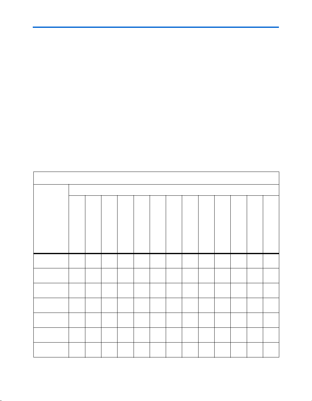
Table 2–5. M4K Memory Capacity & Distribution in Cyclone II Devices
Device M4K Columns M4K Blocks Total RAM Bits
EP2C5 2 26 119,808
EP2C8 2 36 165,888
EP2C15 2 52 239,616
EP2C20 2 52 239,616
EP2C35 3 105 483,840
EP2C50 3 129 594,432
EP2C70 5 250 1,152,000
2–28 Altera Corporation
Cyclone II Device Handbook, Volume 1 February 2007

Cyclone II Architecture
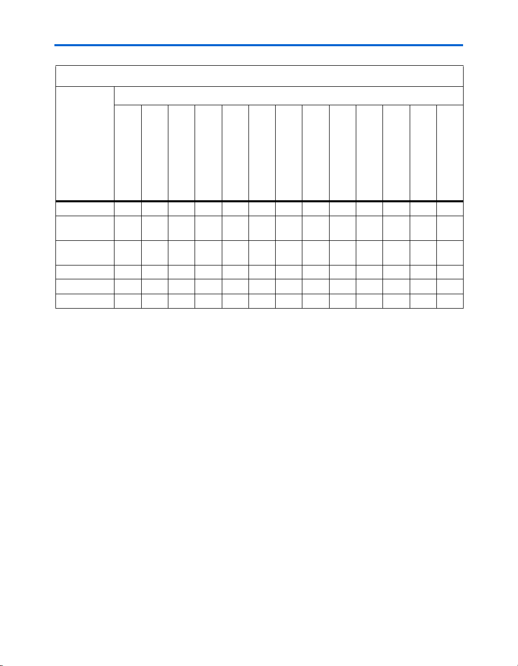
Table 2–6 summarizes the features supported by the M4K memory.
Table 2–6. M4K Memory Features
Feature Description
Maximum performance (1) 250 MHz
Total RAM bits per M4K block (including parity bits) 4,608
Configurations supported 4K × 1
Parity bits One parity bit for each byte. The parity bit, along with
Byte enable M4K blocks support byte writes when the write port has
Packed mode Two single-port memory blocks can be packed into a
Address clock enable M4K blocks support address clock enable, which is
Memory initialization file (.mif) When configured as RAM or ROM, you can use an
Power-up condition Outputs cleared
Register clears Output registers only
Same-port read-during-write New data available at positive clock edge
Mixed-port read-during-write Old data available at positive clock edge
2K × 2
1K × 4
512 × 8
512 × 9
256 × 16
256 × 18
128 × 32 (not available in true dual-port mode)
128 × 36 (not available in true dual-port mode)
internal user logic, can implement parity checking for
error detection to ensure data integrity.
a data width of 1, 2, 4, 8, 9, 16, 18, 32, or 36 bits. The
byte enables allow the input data to be masked so the
device can write to specific bytes. The unwritten bytes
retain the previous written value.
single M4K block if each of the two independent block
sizes are equal to or less than half of the M4K block
size, and each of the single-port memory blocks is
configured in single-clock mode.
used to hold the previous address value for as long as
the signal is enabled. This feature is useful in handling
misses in cache applications.
initialization file to pre-load the memory contents.
Note to Ta b le 2– 6 :
(1) Maximum performance information is preliminary until device characterization.
Altera Corporation 2–29
February 2007 Cyclone II Device Handbook, Volume 1

Embedded Memory
Memory Modes
Table 2–7 summarizes the different memory modes supported by the
M4K memory blocks.
Table 2–7. M4K Memory Modes
Memory Mode Description
Single-port memory M4K blocks support single-port mode, used when
simultaneous reads and writes are not required.
Single-port memory supports non-simultaneous
reads and writes.
Simple dual-port memory Simple dual-port memory supports a
simultaneous read and write.
Simple dual-port with mixed
width
True dual-port memory True dual-port mode supports any combination of
True dual-port with mixed
width
Embedded shift register M4K memory blocks are used to implement shift
ROM The M4K memory blocks support ROM mode. A
FIFO buffers A single clock or dual clock FIFO may be
Simple dual-port memory mode with different
read and write port widths.
two-port operations: two reads, two writes, or one
read and one write at two different clock
frequencies.
True dual-port mode with different read and write
port widths.
registers. Data is written into each address
location at the falling edge of the clock and read
from the address at the rising edge of the clock.
MIF initializes the ROM contents of these blocks.
implemented in the M4K blocks. Simultaneous
read and write from an empty FIFO buffer is not
supported.
1 Embedded Memory can be inferred in your HDL code or
directly instantiated in the Quartus II software using the
®
MegaWizard
2–30 Altera Corporation
Cyclone II Device Handbook, Volume 1 February 2007
Plug-in Manager Memory Compiler feature.

Cyclone II Architecture
Clock Modes
Table 2–8 summarizes the different clock modes supported by the M4K
memory.
Table 2–8. M4K Clock Modes
Clock Mode Description
Independent In this mode, a separate clock is available for each port (ports A
and B). Clock A controls all registers on the port A side, while
clock B controls all registers on the port B side.
Input/output On each of the two ports, A or B, one clock controls all registers
Read/write Up to two clocks are available in this mode. The write clock
Single In this mode, a single clock, together with clock enable, is used to
Table 2–9 shows which clock modes are supported by all M4K blocks
when configured in the different memory modes.
for inputs into the memory block: data input, wren, and address.
The other clock controls the block’s data output registers.
controls the block’s data inputs, wraddress, and wren. The
read clock controls the data output, rdaddress, and rden.
control all registers of the memory block. Asynchronous clear
signals for the registers are not supported.
Table 2–9. Cyclone II M4K Memory Clock Modes
Clocking Modes
Independent v
Input/output vvv
Read/write v
Single clock vvv
True Dual-Port
Mode
Simple Dual-Port
Mode
Single-Port Mode
M4K Routing Interface
The R4, C4, and direct link interconnects from adjacent LABs drive the
M4K block local interconnect. The M4K blocks can communicate with
LABs on either the left or right side through these row resources or with
LAB columns on either the right or left with the column resources. Up to
16 direct link input connections to the M4K block are possible from the
left adjacent LAB and another 16 possible from the right adjacent LAB.
M4K block outputs can also connect to left and right LABs through each
16 direct link interconnects. Figure 2–17 shows the M4K block to logic
array interface.
Altera Corporation 2–31
February 2007 Cyclone II Device Handbook, Volume 1

Embedded Multipliers
Figure 2–17. M4K RAM Block LAB Row Interface
C4 Interconnects
Direct link
interconnect
to adjacent LAB
Direct link
interconnect
from adjacent LAB
16
dataout
M4K RAM
16 16
M4K RAM Block Local
Interconnect Region
Block
Byte enable
Control
Signals
Clocks
datainaddress
6
LAB Row Clocks
R4 Interconnects
Direct link
interconnect
to adjacent LAB
Direct link
interconnect
from adjacent LAB
f For more information on Cyclone II embedded memory, see the
Cyclone II Memory Blocks chapter in Volume 1 of the Cyclone II Device
Handbook.
Embedded
Multipliers
2–32 Altera Corporation
Cyclone II Device Handbook, Volume 1 February 2007
Cyclone II devices have embedded multiplier blocks optimized for
multiplier-intensive digital signal processing (DSP) functions, such as
finite impulse response (FIR) filters, fast Fourier transform (FFT)
functions, and discrete cosine transform (DCT) functions. You can use the
embedded multiplier in one of two basic operational modes, depending
on the application needs:
■ One 18-bit multiplier
■ Up to two independent 9-bit multipliers

Embedded multipliers can operate at up to 250 MHz (for the fastest speed
grade) for 18 × 18 and 9 × 9 multiplications when using both input and
output registers.
Each Cyclone II device has one to three columns of embedded multipliers
that efficiently implement multiplication functions. An embedded
multiplier spans the height of one LAB row. Table 2–10 shows the number
of embedded multipliers in each Cyclone II device and the multipliers
that can be implemented.
Table 2–10. Number of Embedded Multipliers in Cyclone II Devices Note (1)
Cyclone II Architecture
Device
EP2C5 1 13 26 13
EP2C8 1 18 36 18
EP2C15 1 26 52 26
EP2C20 1 26 52 26
EP2C35 1 35 70 35
EP2C50 2 86 172 86
EP2C70 3 150 300 150
Note to Table 2–10:
(1) Each device has either the number of 9 × 9-, or 18 × 18-bit multipliers shown. The total number of multipliers for
each device is not the sum of all the multipliers.
Embedded
Multiplier Columns
Embedded
Multipliers
9 × 9 Multipliers 18 × 18 Multipliers
The embedded multiplier consists of the following elements:
■ Multiplier block
■ Input and output registers
■ Input and output interfaces
Figure 2–18 shows the multiplier block architecture.
Altera Corporation 2–33
February 2007 Cyclone II Device Handbook, Volume 1

Embedded Multipliers
Figure 2–18. Multiplier Block Architecture
signa
signb
aclr
clock
ena
(1)
(1)
Data A
Data B
DQ
ENA
CLRN
DQ
ENA
CLRN
Input
Register
Embedded Multiplier Block
DQ
ENA
CLRN
Output
Register
Note to Figure 2–18:
(1) If necessary, these signals can be registered once to match the data signal path.
Each multiplier operand can be a unique signed or unsigned number.
Two signals, signa and signb, control the representation of each
operand respectively. A logic 1 value on the signa signal indicates that
data A is a signed number while a logic 0 value indicates an unsigned
number. Table 2–11 shows the sign of the multiplication result for the
various operand sign representations. The result of the multiplication is
signed if any one of the operands is a signed value.
Table 2–11. Multiplier Sign Representation
Data A (signa Value) Data B (signb Value) Result
Unsigned Unsigned Unsigned
Unsigned Signed Signed
Signed Unsigned Signed
Signed Signed Signed
Data Out
2–34 Altera Corporation
Cyclone II Device Handbook, Volume 1 February 2007

Cyclone II Architecture
There is only one signa and one signb signal for each dedicated
multiplier. Therefore, all of the data A inputs feeding the same dedicated
multiplier must have the same sign representation. Similarly, all of the
data B inputs feeding the same dedicated multiplier must have the same
sign representation. The signa and signb signals can be changed
dynamically to modify the sign representation of the input operands at
run time. The multiplier offers full precision regardless of the sign
representation and can be registered using dedicated registers located at
the input register stage.
Multiplier Modes
Table 2–12 summarizes the different modes that the embedded
multipliers can operate in.
Table 2–12. Embedded Multiplier Modes
Multiplier Mode Description
18-bit Multiplier An embedded multiplier can be configured to support a
single 18 × 18 multiplier for operand widths up to 18 bits.
All 18-bit multiplier inputs and results can be registered
independently. The multiplier operands can accept
signed integers, unsigned integers, or a combination of
both.
9-bit Multiplier An embedded multiplier can be configured to support
two 9 × 9 independent multipliers for operand widths up
to 9-bits. Both 9-bit multiplier inputs and results can be
registered independently. The multiplier operands can
accept signed integers, unsigned integers or a
combination of both.
There is only one signa signal to control the sign
representation of both data A inputs and one signb
signal to control the sign representation of both data B
inputs of the 9-bit multipliers within the same dedicated
multiplier.
Altera Corporation 2–35
February 2007 Cyclone II Device Handbook, Volume 1

Embedded Multipliers
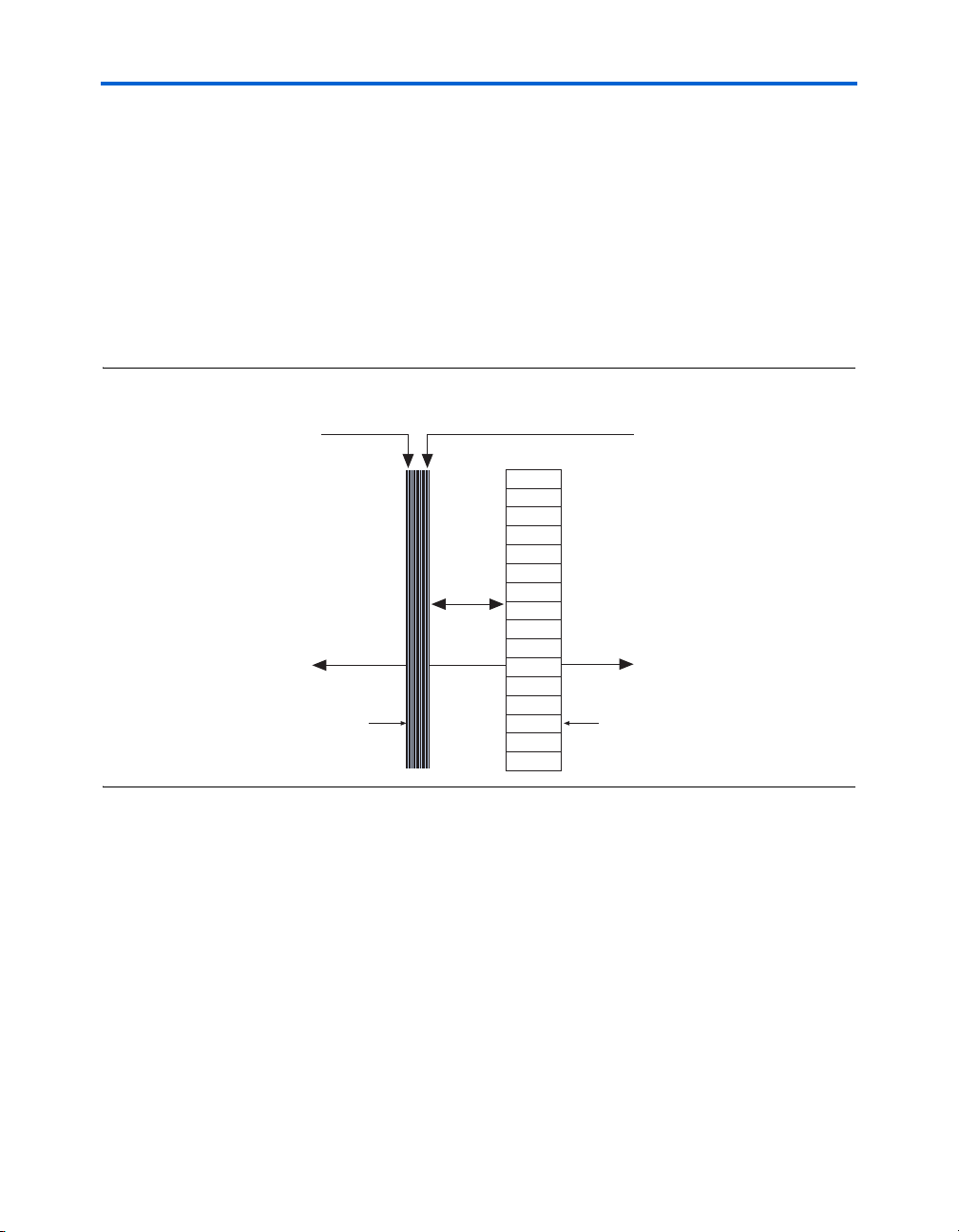
Embedded Multiplier Routing Interface
The R4, C4, and direct link interconnects from adjacent LABs drive the
embedded multiplier row interface interconnect. The embedded
multipliers can communicate with LABs on either the left or right side
through these row resources or with LAB columns on either the right or
left with the column resources. Up to 16 direct link input connections to
the embedded multiplier are possible from the left adjacent LABs and
another 16 possible from the right adjacent LAB. Embedded multiplier
outputs can also connect to left and right LABs through 18 direct link
interconnects each. Figure 2–19 shows the embedded multiplier to logic
array interface.
Figure 2–19. Embedded Multiplier LAB Row Interface
Direct Link Interconnect
from Adjacent LAB
R4 InterconnectsC4 Interconnects
18 Direct Link Outputs
to Adjacent LABs
36
Direct Link Interconnect
from Adjacent LAB
LAB Block
Interconect Region
LAB LAB
16
5
36
Row Interface
Block
Embedded Multiplier
to LAB Row Interface
Block Interconnect Region
36 Inputs per Row 36 Outputs per Row
Embedded Multiplier
18
16
Control
[35..0][35..0]
18 18
C4 Interconnects
18
LAB Block
Interconect Region
2–36 Altera Corporation
Cyclone II Device Handbook, Volume 1 February 2007

Cyclone II Architecture
There are five dynamic control input signals that feed the embedded
multiplier: signa, signb, clk, clkena, and aclr. signa and signb
can be registered to match the data signal input path. The same clk,
clkena, and aclr signals feed all registers within a single embedded
multiplier.
f For more information on Cyclone II embedded multipliers, see the
Embedded Multipliers in Cyclone II Devices chapter.
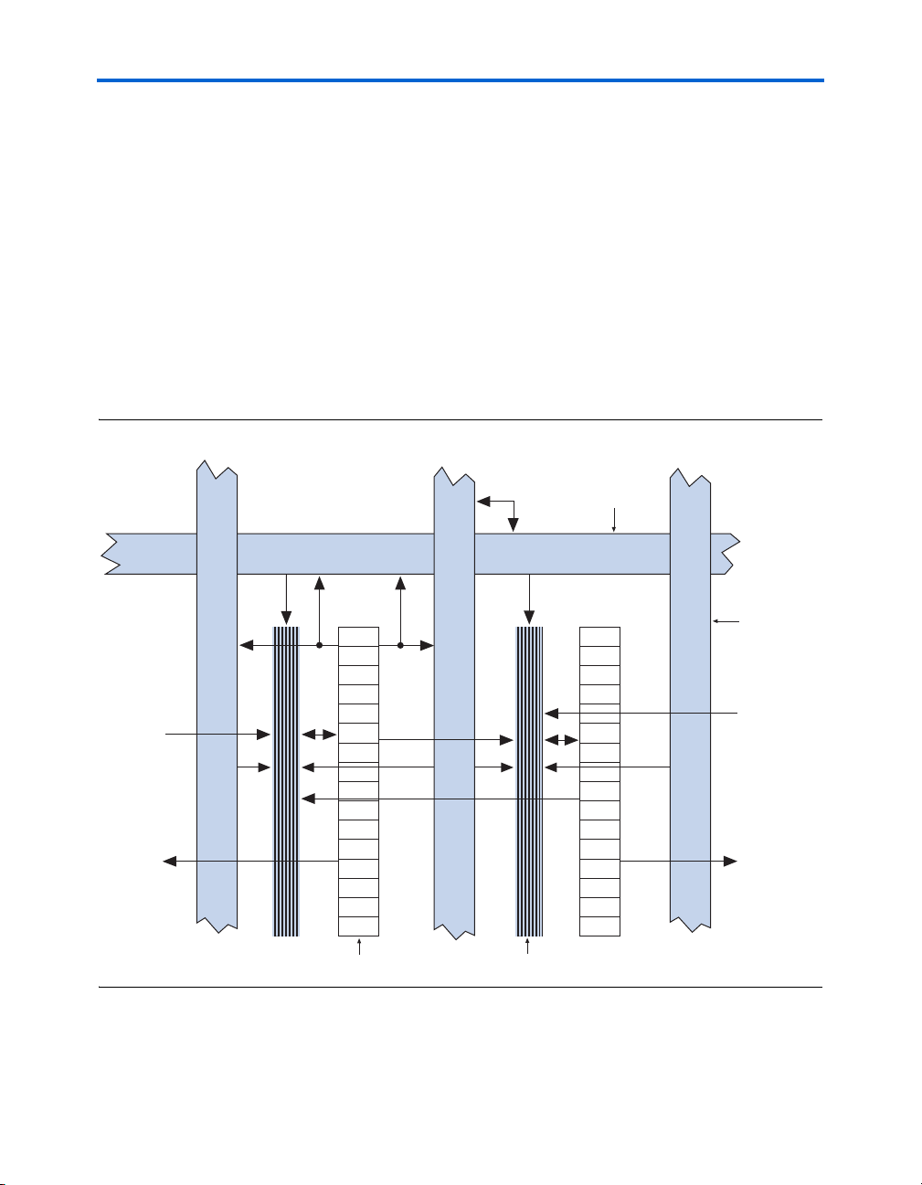
I/O Structure & Features
IOEs support many features, including:
■ Differential and single-ended I/O standards
■ 3.3-V, 64- and 32-bit, 66- and 33-MHz PCI compliance
■ Joint Test Action Group (JTAG) boundary-scan test (BST) support
■ Output drive strength control
■ Weak pull-up resistors during configuration
■ Tri-state buffers
■ Bus-hold circuitry
■ Programmable pull-up resistors in user mode
■ Programmable input and output delays
■ Open-drain outputs
■ DQ and DQS I/O pins
■ V
REF
pins
Cyclone II device IOEs contain a bidirectional I/O buffer and three
registers for complete embedded bidirectional single data rate transfer.
Figure 2–20 shows the Cyclone II IOE structure. The IOE contains one
input register, one output register, and one output enable register. You can
use the input registers for fast setup times and output registers for fast
clock-to-output times. Additionally, you can use the output enable (OE)
register for fast clock-to-output enable timing. The Quartus II software
automatically duplicates a single OE register that controls multiple
output or bidirectional pins. You can use IOEs as input, output, or
bidirectional pins.
Altera Corporation 2–37
February 2007 Cyclone II Device Handbook, Volume 1

I/O Structure & Features
Figure 2–20. Cyclone II IOE Structure
Logic Array
OE Register
OE
Output Register
Output
Input (1)
Input Register
Note to Figure 2–20:
(1) There are two paths available for combinational or registered inputs to the logic
array. Each path contains a unique programmable delay chain.
The IOEs are located in I/O blocks around the periphery of the Cyclone II
device. There are up to five IOEs per row I/O block and up to four IOEs
per column I/O block (column I/O blocks span two columns). The row
I/O blocks drive row, column (only C4 interconnects), or direct link
interconnects. The column I/O blocks drive column interconnects.
Figure 2–21 shows how a row I/O block connects to the logic array.
Figure 2–22 shows how a column I/O block connects to the logic array.
2–38 Altera Corporation
Cyclone II Device Handbook, Volume 1 February 2007

Figure 2–21. Row I/O Block Connection to the Interconnect
)
Cyclone II Architecture
R4 & R24 Interconnects
Direct Link
Interconnect
to Adjacent LAB
LAB Local
Interconnect
LAB
C4 Interconnects
io_datain0[4..0]
io_datain1[4..0] (2)
Direct Link
Interconnect
from Adjacent LAB
I/O Block Local
Interconnect
35
io_clk[5..0]
35 Data and
Control Signals
from Logic Array (1
Row
I/O Block
Row I/O Block
Contains up to
Five IOEs
Notes to Figure 2–21:
(1) The 35 data and control signals consist of five data out lines, io_dataout[4..0], five output enables,
io_coe[4..0], five input clock enables, io_cce_in[4..0], five output clock enables, io_cce_out[4..0],
five clocks, io_cclk[4..0], five asynchronous clear signals, io_caclr[4..0], and five synchronous clear
signals, io_csclr[4..0].
(2) Each of the five IOEs in the row I/O block can have two io_datain (combinational or registered) inputs.
Altera Corporation 2–39
February 2007 Cyclone II Device Handbook, Volume 1

I/O Structure & Features
s
Figure 2–22. Column I/O Block Connection to the Interconnect
28 Data &
Control Signals
from Logic Array (1)
28
I/O Block
Local Interconnect
R4 & R24 Interconnects
Column I/O Block
io_datain0[3..0]
io_datain1[3..0] (2)
Column I/O
Block Contains
up to Four IOE
io_clk[5..0]
LAB LAB LAB
LAB Local
Interconnect
C4 & C24 Interconnects
Notes to Figure 2–22:
(1) The 28 data and control signals consist of four data out lines, io_dataout[3..0], four output enables,
io_coe[3..0], four input clock enables, io_cce_in[3..0], four output clock enables, io_cce_out[3..0],
four clocks, io_cclk[3..0], four asynchronous clear signals, io_caclr[3..0], and four synchronous clear
signals, io_csclr[3..0].
(2) Each of the four IOEs in the column I/O block can have two io_datain (combinational or registered) inputs.
2–40 Altera Corporation
Cyclone II Device Handbook, Volume 1 February 2007

The pin’s datain signals can drive the logic array. The logic array drives
the control and data signals, providing a flexible routing resource. The
row or column IOE clocks, io_clk[5..0], provide a dedicated routing
resource for low-skew, high-speed clocks. The global clock network
generates the IOE clocks that feed the row or column I/O regions (see
“Global Clock Network & Phase-Locked Loops” on page 2–16).
Figure 2–23 illustrates the signal paths through the I/O block.
Figure 2–23. Signal Path Through the I/O Block
Row or Column
io_clk[5..0]
Cyclone II Architecture
To Other
IOEs
To Logic
Array
From Logic
Array
io_datain0
io_datain1
io_csclr
io_coe
io_cce_in
io_cce_out
io_caclr
io_cclk
io_dataout
oe
ce_in
ce_out
Data and
Control
Signal
Selection
aclr/preset
sclr/preset
clk_in
clk_out
dataout
IOE
Each IOE contains its own control signal selection for the following
control signals: oe, ce_in, ce_out, aclr/preset, sclr/preset,
clk_in, and clk_out. Figure 2–24 illustrates the control signal
selection.
Altera Corporation 2–41
February 2007 Cyclone II Device Handbook, Volume 1
I/O Structure & Features
Figure 2–24. Control Signal Selection per IOE
Dedicated I/O
Clock [5..0]
Local
Interconnect
Local
Interconnect
Local
Interconnect
Local
Interconnect
Local
Interconnect
Local
Interconnect
io_coe
io_csclr
io_caclr
io_cce_out
io_cce_in
io_cclk
clk_out
ce_inclk_in
ce_out
sclr/preset
aclr/preset
In normal bidirectional operation, you can use the input register for input
data requiring fast setup times. The input register can have its own clock
input and clock enable separate from the OE and output registers. You can
use the output register for data requiring fast clock-to-output
performance. The OE register is available for fast clock-to-output enable
timing. The OE and output register share the same clock source and the
same clock enable source from the local interconnect in the associated
LAB, dedicated I/O clocks, or the column and row interconnects. All
registers share sclr and aclr, but each register can individually disable
sclr and aclr. Figure 2–25 shows the IOE in bidirectional
configuration.
oe
2–42 Altera Corporation
Cyclone II Device Handbook, Volume 1 February 2007

Figure 2–25. Cyclone II IOE in Bidirectional I/O Configuration
io_clk[5..0]
Column
or Row
Interconect
OE
OE Register
PRN
clkout
ce_out
aclr/prn
Chip-Wide Reset
sclr/preset
DQ
ENA
CLRN
Output Register
PRN
DQ
ENA
CLRN
Output
Pin Delay
Open-Drain Output
Cyclone II Architecture
V
CCIO
Optional
PCI Clamp
V
CCIO
Programmable
Pull-Up
Resistor
data_in1
Bus Hold
data_in0
Input Pin to
Input Register Delay
or Input Pin to
Logic Array Delay
clkin
ce_in
Input Register
PRN
DQ
ENA
CLRN
The Cyclone II device IOE includes programmable delays to ensure zero
hold times, minimize setup times, or increase clock to output times.
A path in which a pin directly drives a register may require a
programmable delay to ensure zero hold time, whereas a path in which a
pin drives a register through combinational logic may not require the
delay. Programmable delays decrease input-pin-to-logic-array and IOE
input register delays. The Quartus II Compiler can program these delays
to automatically minimize setup time while providing a zero hold time.
Altera Corporation 2–43
February 2007 Cyclone II Device Handbook, Volume 1

I/O Structure & Features
Programmable delays can increase the register-to-pin delays for output
registers. Table 2–13 shows the programmable delays for Cyclone II
devices.
Table 2–13. Cyclone II Programmable Delay Chain
Programmable Delays Quartus II Logic Option
Input pin to logic array delay Input delay from pin to internal cells
Input pin to input register delay Input delay from pin to input register
Output pin delay Delay from output register to output pin
There are two paths in the IOE for an input to reach the logic array. Each
of the two paths can have a different delay. This allows you to adjust
delays from the pin to internal LE registers that reside in two different
areas of the device. You set the two combinational input delays by
selecting different delays for two different paths under the Input delay
from pin to internal cells logic option in the Quartus II software.
However, if the pin uses the input register, one of delays is disregarded
because the IOE only has two paths to internal logic. If the input register
is used, the IOE uses one input path. The other input path is then
available for the combinational path, and only one input delay
assignment is applied.
The IOE registers in each I/O block share the same source for clear or
preset. You can program preset or clear for each individual IOE, but both
features cannot be used simultaneously. You can also program the
registers to power up high or low after configuration is complete. If
programmed to power up low, an asynchronous clear can control the
registers. If programmed to power up high, an asynchronous preset can
control the registers. This feature prevents the inadvertent activation of
another device’s active-low input upon power up. If one register in an
IOE uses a preset or clear signal then all registers in the IOE must use that
same signal if they require preset or clear. Additionally a synchronous
reset signal is available for the IOE registers.
External Memory Interfacing
Cyclone II devices support a broad range of external memory interfaces
such as SDR SDRAM, DDR SDRAM, DDR2 SDRAM, and QDRII SRAM
external memories. Cyclone II devices feature dedicated high-speed
interfaces that transfer data between external memory devices at up to
167 MHz/333 Mbps for DDR and DDR2 SDRAM devices and
167 MHz/667 Mbps for QDRII SRAM devices. The programmable DQS
delay chain allows you to fine tune the phase shift for the input clocks or
strobes to properly align clock edges as needed to capture data.
2–44 Altera Corporation
Cyclone II Device Handbook, Volume 1 February 2007

In Cyclone II devices, all the I/O banks support SDR and DDR SDRAM
memory up to 167 MHz/333 Mbps. All I/O banks support DQS signals
with the DQ bus modes of ×8/×9, or ×16/×18. Table 2–14 shows the
external memory interfaces supported in Cyclone II devices.
Table 2–14. External Memory Support in Cyclone II Devices Note (1)
Cyclone II Architecture
Memory Standard I/O Standard
SDR SDRAM LVTTL (2) 72 167 167
DDR SDRAM SSTL-2 class I (2) 72 167 333 (1)
SSTL-2 class II (2) 72 133 267 (1)
DDR2 SDRAM SSTL-18 class I (2) 72 167 333 (1)
SSTL-18 class II (3) 72 125 250 (1)
QDRII SRAM (4) 1.8-V HSTL class I
(2)
1.8-V HSTL class II
(3)
Notes to Table 2–14:
(1) The data rate is for designs using the Clock Delay Control circuitry.
(2) The I/O standards are supported on all the I/O banks of the Cyclone II device.
(3) The I/O standards are supported only on the I/O banks on the top and bottom of the Cyclone II device.
(4) For maximum performance, Altera recommends using the 1.8-V HSTL I/O standard because of higher I/O drive
strength. QDRII SRAM devices also support the 1.5-V HSTL I/O standard.
Maximum Bus
Width
36 167 668 (1)
36 100 400 (1)
Maximum Clock
Rate Supported
(MHz)
Maximum Data
Rate Supported
(Mbps)
Cyclone II devices use data (DQ), data strobe (DQS), and clock pins to
interface with external memory. Figure 2–26 shows the DQ and DQS pins
in the ×8/×9 mode.
Altera Corporation 2–45
February 2007 Cyclone II Device Handbook, Volume 1

I/O Structure & Features
Figure 2–26. Cyclone II Device DQ & DQS Groups in ×8/×9 Mode Notes (1), (2)
DQ Pins DQS Pin DM PinDQ Pins
Notes to Figure 2–26:
(1) Each DQ group consists of a DQS pin, DM pin, and up to nine DQ pins.
(2) This is an idealized pin layout. For actual pin layout, refer to the pin table.
(2)
Cyclone II devices support the data strobe or read clock signal (DQS)
used in DDR and DDR2 SDRAM. Cyclone II devices can use either
bidirectional data strobes or unidirectional read clocks. The dedicated
external memory interface in Cyclone II devices also includes
programmable delay circuitry that can shift the incoming DQS signals to
center align the DQS signals within the data window.
The DQS signal is usually associated with a group of data (DQ) pins. The
phase-shifted DQS signals drive the global clock network, which is used
to clock the DQ signals on internal LE registers.
Table 2–15 shows the number of DQ pin groups per device.
Table 2–15. Cyclone II DQS & DQ Bus Mode Support (Part 1 of 2) Note (1)
Device Package
EP2C5 144-pin TQFP (2) 3 300
208-pin PQFP 7 (3) 433
EP2C8 144-pin TQFP (2) 3 300
208-pin PQFP 7 (3) 433
256-pin FineLine BGA
EP2C15 256-pin FineLine BGA 8 4 4 4
484-pin FineLine BGA 16 (4) 888
EP2C20 256-pin FineLine BGA 8 4 4 4
484-pin FineLine BGA 16 (4) 888
Number of ×8
Groups
®
8 (3) 444
Number of ×9
Groups (5), (6)
Number of ×16
Groups
Number of ×18
Groups (5), (6)
2–46 Altera Corporation
Cyclone II Device Handbook, Volume 1 February 2007

Table 2–15. Cyclone II DQS & DQ Bus Mode Support (Part 2 of 2) Note (1)
Cyclone II Architecture
Device Package
EP2C35 484-pin FineLine BGA 16 (4) 888
672-pin FineLine BGA 20 (4) 888
EP2C50 484-pin FineLine BGA 16 (4) 888
672-pin FineLine BGA 20 (4) 888
EP2C70 672-pin FineLine BGA 20 (4) 888
896-pin FineLine BGA 20 (4) 888
Notes to Table 2–15:
(1) Numbers are preliminary.
(2) EP2C5 and EP2C8 devices in the 144-pin TQFP package do not have any DQ pin groups in I/O bank 1.
(3) Because of available clock resources, only a total of 6 DQ/DQS groups can be implemented.
(4) Because of available clock resources, only a total of 14 DQ/DQS groups can be implemented.
(5) The ×9 DQS/DQ groups are also used as ×8 DQS/DQ groups. The ×18 DQS/DQ groups are also used as ×16
DQS/DQ groups.
(6) For QDRI implementation, if you connect the D ports (write data) to the Cyclone II DQ pins, the total available ×9
DQS /DQ and ×18 DQS/DQ groups are half of that shown in Table 2–15.
Number of ×8
Groups
Number of ×9
Groups (5), (6)
Number of ×16
Groups
Number of ×18
Groups (5), (6)
You can use any of the DQ pins for the parity pins in Cyclone II devices.
The Cyclone II device family supports parity in the ×8/×9, and ×16/×18
mode. There is one parity bit available per eight bits of data pins.
The data mask, DM, pins are required when writing to DDR SDRAM and
DDR2 SDRAM devices. A low signal on the DM pin indicates that the
write is valid. If the DM signal is high, the memory masks the DQ signals.
In Cyclone II devices, the DM pins are assigned and are the preferred
pins. Each group of DQS and DQ signals requires a DM pin.
When using the Cyclone II I/O banks to interface with the DDR memory,
at least one PLL with two clock outputs is needed to generate the system
and write clock. The system clock is used to clock the DQS write signals,
commands, and addresses. The write clock is shifted by –90° from the
system clock and is used to clock the DQ signals during writes.
Figure 2–27 illustrates DDR SDRAM interfacing from the I/O through
the dedicated circuitry to the logic array.
Altera Corporation 2–47
February 2007 Cyclone II Device Handbook, Volume 1

I/O Structure & Features
Figure 2–27. DDR SDRAM Interfacing
DQS
DQ
PLL
OE
-90˚ Shifted clk
LE
Register
Register
t
LE
LE
V
CC
Register
LE
GND
Register
clk
Clock Delay
Control Circuitry
Clock Control
Block
LE
OE
Register
LE
Register
en/dis
ENOUT ena_register_mode
LE
DataA
Register
LE
DataB
Register
Global Clock
Dynamic Enable/Disable
Circuitry
LE
Register
LE
RegisterLERegisterLERegister
f For more information on Cyclone II external memory interfaces, see the
External Memory Interfaces chapter in Volume 1 of the Cyclone II Device
Handbook.
Adjacent LAB LEs
LE
Register
Resynchronizing
to System Clock
2–48 Altera Corporation
Cyclone II Device Handbook, Volume 1 February 2007

Cyclone II Architecture
Programmable Drive Strength
The output buffer for each Cyclone II device I/O pin has a programmable
drive strength control for certain I/O standards. The LVTTL, LVCMOS,
SSTL-2 class I and II, SSTL-18 class I and II, HSTL-18 class I and II, and
HSTL-1.5 class I and II standards have several levels of drive strength that
you can control. Using minimum settings provides signal slew rate
control to reduce system noise and signal overshoot. Table 2–16 shows
the possible settings for the I/O standards with drive strength control.
Table 2–16. Programmable Drive Strength (Part 1 of 2) Note (1)
Current Strength Setting (mA)
I
I/O Standard
LVTTL (3.3 V) 4 4
LVCMOS (3.3 V) 4 4
LVTTL/LVCMOS (2.5 V) 4 4
LVTTL/LVCMOS (1.8 V) 2 2
OH/IOL
Top & Bottom I/O Pins Side I/O Pins
88
12 12
16 16
20 20
24 24
88
12 12
16
20
24
88
12
16
44
66
88
10 10
12 12
Altera Corporation 2–49
February 2007 Cyclone II Device Handbook, Volume 1

I/O Structure & Features
Table 2–16. Programmable Drive Strength (Part 2 of 2) Note (1)
I
Current Strength Setting (mA)
I/O Standard
OH/IOL
Top & Bottom I/O Pins Side I/O Pins
LVCMOS (1.5 V) 2 2
44
66
8
SSTL-2 class I 8 8
12 12
SSTL-2 class II 16 16
20
24
SSTL-18 class I 6 6
88
10 10
12
SSTL-18 class II 16
18
HSTL-18 class I 8 8
10 10
12 12
HSTL-18 class II 16
18
20
HSTL-15 class I 8 8
10
12
HSTL-15 class II 16
Note to Table 2–16:
(1) The default current in the Quartus II software is the maximum setting for each
I/O standard.
Open-Drain Output
Cyclone II devices provide an optional open-drain (equivalent to an
open-collector) output for each I/O pin. This open-drain output enables
the device to provide system-level control signals (that is, interrupt and
write-enable signals) that can be asserted by any of several devices.
2–50 Altera Corporation
Cyclone II Device Handbook, Volume 1 February 2007

Cyclone II Architecture
Slew Rate Control
Slew rate control is performed by using programmable output drive
strength.
Bus Hold
Each Cyclone II device user I/O pin provides an optional bus-hold
feature. The bus-hold circuitry can hold the signal on an I/O pin at its
last-driven state. Since the bus-hold feature holds the last-driven state of
the pin until the next input signal is present, an external pull-up or
pull-down resistor is not necessary to hold a signal level when the bus is
tri-stated.
The bus-hold circuitry also pulls undriven pins away from the input
threshold voltage where noise can cause unintended high-frequency
switching. You can select this feature individually for each I/O pin. The
bus-hold output drives no higher than V
signals.
1 If the bus-hold feature is enabled, the device cannot use the
programmable pull-up option. Disable the bus-hold feature
when the I/O pin is configured for differential signals. Bus hold
circuitry is not available on the dedicated clock pins.
to prevent overdriving
CCIO
The bus-hold circuitry is only active after configuration. When going into
user mode, the bus-hold circuit captures the value on the pin present at
the end of configuration.
The bus-hold circuitry uses a resistor with a nominal resistance (R
BH
) of
approximately 7 kΩ to pull the signal level to the last-driven state. Refer
to the DC Characteristics & Timing Specifications chapter in Volume 1 of the
Cyclone II Device Handbook for the specific sustaining current for each
voltage level driven through the resistor and overdrive current
V
CCIO
used to identify the next driven input level.
Programmable Pull-Up Resistor
Each Cyclone II device I/O pin provides an optional programmable
pull-up resistor during user mode. If you enable this feature for an I/O
pin, the pull-up resistor (typically 25 kΩ) holds the output to the V
level of the output pin’s bank.
1 If the programmable pull-up is enabled, the device cannot use
the bus-hold feature. The programmable pull-up resistors are
not supported on the dedicated configuration, JTAG, and
dedicated clock pins.
Altera Corporation 2–51
February 2007 Cyclone II Device Handbook, Volume 1
CCIO

I/O Structure & Features
Advanced I/O Standard Support
Table 2–17 shows the I/O standards supported by Cyclone II devices and
which I/O pins support them.
Table 2–17. Cyclone II Supported I/O Standards & Constraints (Part 1 of 2)
V
Level
CCIO
I/O Standard Type
Input Output
3.3-V LVTTL and LVCMOS
(1)
2.5-V LVTTL and LVCMOS Single ended 3.3 V/
1.8-V LVTTL and LVCMOS Single ended 1.8 V/
1.5-V LVCMOS Single ended 1.8 V/
SSTL-2 class I Voltage
SSTL-2 class II Voltage
SSTL-18 class I Voltage
SSTL-18 class II Voltage
HSTL-18 class I Voltage
HSTL-18 class II Voltage
HSTL-15 class I Voltage
HSTL-15 class II Voltage
PCI and PCI-X (1) (3) Single ended 3.3 V 3.3 V
Differential SSTL-2 class I or
class II
Differential SSTL-18 class I
or class II
Single ended 3.3 V/
referenced
referenced
referenced
referenced
referenced
referenced
referenced
referenced
Pseudo
differential (4)
Pseudo
differential (4)
2.5 V
2.5 V
1.5 V
1.5 V
2.5 V 2.5 V
2.5 V 2.5 V
1.8 V 1.8 V
1.8 V 1.8 V
1.8 V 1.8 V
1.8 V 1.8 V
1.5 V 1.5 V
1.5 V 1.5 V
(5) 2.5 V
2.5 V (5)
(5) 1.8 V
1.8 V (5)
3.3 V
2.5 V
1.8 V
1.5 V
Top & Bottom
I/O Pins
CLK,
User I/O
DQS
Pins
CLK,
DQS
Side I/O Pins
PLL_OUT
User I/O
Pins
vvv v v
vvv v v
vvv v v
vvv v v
vvv v v
vvv v v
vvv v v
vv
(2) (2) (2)
vvv v v
vv
(2) (2) (2)
vvv v v
vv
(2) (2) (2)
vv v
v
v
(6)
v
(6)
v (7)
v
(6)
v
(6)
2–52 Altera Corporation
Cyclone II Device Handbook, Volume 1 February 2007

Table 2–17. Cyclone II Supported I/O Standards & Constraints (Part 2 of 2)
Cyclone II Architecture
V
Level
CCIO
Top & Bottom
I/O Pins
Side I/O Pins
I/O Standard Type
CLK,
Input Output
Differential HSTL-15 class I
or class II
Differential HSTL-18 class I
or class II
LVDS Differential 2.5 V 2.5 V
RSDS and mini-LVDS (8) Differential (5) 2.5 V
LVPECL (9) Differential 3.3 V/
Notes to Table 2–17:
(1) To drive inputs higher than V
LVTTL and LVCMOS input levels to overdrive input buffer option in the Quartus II software.
(2) These pins support SSTL-18 class II and 1.8- and 1.5-V HSTL class II inputs.
(3) PCI-X does not meet the IV curve requirement at the linear region. PCI-clamp diode is not available on top and
bottom I/O pins.
(4) Pseudo-differential HSTL and SSTL outputs use two single-ended outputs with the second output programmed
as inverted. Pseudo-differential HSTL and SSTL inputs treat differential inputs as two single-ended HSTL and
SSTL inputs and only decode one of them.
(5) This I/O standard is not supported on these I/O pins.
(6) This I/O standard is only supported on the dedicated clock pins.
(7) PLL_OUT does not support differential SSTL-18 class II and differential 1.8 and 1.5-V HSTL class II.
(8) mini-LVDS and RSDS are only supported on output pins.
(9) LVPECL is only supported on clock inputs.
Pseudo
differential (4)
Pseudo
differential (4)
but less than 4.0 V, disable the PCI clamping diode and turn on the Allow
CCIO
(5) 1.5 V
1.5 V (5)
(5) 1.8 V
1.8 V (5)
(5)
2.5 V/
1.8 V/
1.5 V
User I/O
DQS
v
(6)
v
(6)
vvv v v
vv
Pins
CLK,
DQS
PLL_OUT
User I/O
Pins
v (7)
v
(6)
v (7)
v
(6)
vvv
f For more information on Cyclone II supported I/O standards, see the
Selectable I/O Standards in Cyclone II Devices chapter in Volume 1 of the
Cyclone II Device Handbook.
High-Speed Differential Interfaces
Cyclone II devices can transmit and receive data through LVDS signals at
a data rate of up to 640 Mbps and 805 Mbps, respectively. For the LVDS
transmitter and receiver, the Cyclone II device’s input and output pins
support serialization and deserialization through internal logic.
Altera Corporation 2–53
February 2007 Cyclone II Device Handbook, Volume 1

I/O Structure & Features
The reduced swing differential signaling (RSDS) and mini-LVDS
standards are derivatives of the LVDS standard. The RSDS and
mini-LVDS I/O standards are similar in electrical characteristics to
LVDS, but have a smaller voltage swing and therefore provide increased
power benefits and reduced electromagnetic interference (EMI).
Cyclone II devices support the RSDS and mini-LVDS I/O standards at
data rates up to 311 Mbps at the transmitter.
A subset of pins in each I/O bank (on both rows and columns) support
the high-speed I/O interface. The dual-purpose LVDS pins require an
external-resistor network at the transmitter channels in addition to 100-Ω
termination resistors on receiver channels. These pins do not contain
dedicated serialization or deserialization circuitry. Therefore, internal
logic performs serialization and deserialization functions.
Cyclone II pin tables list the pins that support the high-speed I/O
interface. The number of LVDS channels supported in each device family
member is listed in Table 2–18.
Table 2–18. Cyclone II Device LVDS Channels (Part 1 of 2)
Device Pin Count
EP2C5 144 31 (35)
208 56 (60)
256 61 (65)
EP2C8 144 29 (33)
208 53 (57)
256 75 (79)
EP2C15 256 52 (60)
484 128 (136)
EP2C20 240 45 (53)
256 52 (60)
484 128 (136)
EP2C35 484 131 (139)
672 201 (209)
EP2C50 484 119 (127)
672 189 (197)
Number of LVDS
Channels (1)
2–54 Altera Corporation
Cyclone II Device Handbook, Volume 1 February 2007

Cyclone II Architecture
Table 2–18. Cyclone II Device LVDS Channels (Part 2 of 2)
Device Pin Count
EP2C70 672 160 (168)
896 257 (265)
Note to Table 2–18:
(1) The first number represents the number of bidirectional I/O pins which can be
used as inputs or outputs. The number in parenthesis includes dedicated clock
input pin pairs which can only be used as inputs.
Number of LVDS
Channels (1)
You can use I/O pins and internal logic to implement a high-speed I/O
receiver and transmitter in Cyclone II devices. Cyclone II devices do not
contain dedicated serialization or deserialization circuitry. Therefore,
shift registers, internal PLLs, and IOEs are used to perform
serial-to-parallel conversions on incoming data and parallel-to-serial
conversion on outgoing data.
The maximum internal clock frequency for a receiver and for a
transmitter is 402.5 MHz. The maximum input data rate of 805 Mbps and
the maximum output data rate of 640 Mbps is only achieved when DDIO
registers are used. The LVDS standard does not require an input
reference voltage, but it does require a 100-Ω termination resistor
between the two signals at the input buffer. An external resistor network
is required on the transmitter side.
f For more information on Cyclone II differential I/O interfaces, see the
High-Speed Differential Interfaces in Cyclone II Devices chapter in Volume 1
of the Cyclone II Device Handbook.
Series On-Chip Termination
On-chip termination helps to prevent reflections and maintain signal
integrity. This also minimizes the need for external resistors in high pin
count ball grid array (BGA) packages. Cyclone II devices provide I/O
driver on-chip impedance matching and on-chip series termination for
single-ended outputs and bidirectional pins.
Altera Corporation 2–55
February 2007 Cyclone II Device Handbook, Volume 1

I/O Structure & Features
Cyclone II devices support driver impedance matching to the impedance
of the transmission line, typically 25 or 50 Ω. When used with the output
drivers, on-chip termination sets the output driver impedance to 25 or
50 Ω. Cyclone II devices also support I/O driver series termination
= 50 Ω) for SSTL-2 and SSTL-18. Table 2–19 lists the I/O standards that
(R
S
support impedance matching and series termination.
Table 2–19. I/O Standards Supporting Series Termination Note (1)
I/O Standards
3.3-V LVTTL and LVCMOS 25 (2) 3.3
2.5-V LVTTL and LVCMOS 50 (2) 2.5
1.8-V LVTTL and LVCMOS 50 (2) 1.8
SSTL-2 class I 50 (2) 2.5
SSTL-18 class I 50 (2) 1.8
Notes to Ta b l e 2 – 1 9 :
(1) Supported conditions are V
(2) These RS values are nominal values. Actual impedance varies across process,
voltage, and temperature conditions.
Target R
CCIO=VCCIO
(Ω)V
S
±50 mV.
CCIO
(V)
1 The recommended frequency range of operation is pending
silicon characterization.
On-chip series termination can be supported on any I/O bank. V
V
must be compatible for all I/O pins in order to enable on-chip series
REF
CCIO
and
termination in a given I/O bank. I/O standards that support different RS
value s can reside in the sa me I/O bank as long as the ir V
CCIO
and V
REF
are
not conflicting.
1 When using on-chip series termination, programmable drive
strength is not available.
Impedance matching is implemented using the capabilities of the output
driver and is subject to a certain degree of variation, depending on the
process, voltage and temperature. The actual tolerance is pending silicon
characterization.
2–56 Altera Corporation
Cyclone II Device Handbook, Volume 1 February 2007

Cyclone II Architecture
I/O Banks
The I/O pins on Cyclone II devices are grouped together into I/O banks
and each bank has a separate power bus. EP2C5 and EP2C8 devices have
four I/O banks (see Figure 2–28), while EP2C15, EP2C20, EP2C35,
EP2C50, and EP2C70 devices have eight I/O banks (see Figure 2–29).
Each device I/O pin is associated with one I/O bank. To accommodate
voltage-referenced I/O standards, each Cyclone II I/O bank has a VREF
bus. Each bank in EP2C5, EP2C8, EP2C15, EP2C20, EP2C35, and EP2C50
devices supports two VREF pins and each bank of EP2C70 supports four
VREF pins. When using the VREF pins, each VREF pin must be properly
connected to the appropriate voltage level. In the event these pins are not
used as VREF pins, they may be used as regular I/O pins.
The top and bottom I/O banks (banks 2 and 4 in EP2C5 and EP2C8
devices and banks 3, 4, 7, and 8 in EP2C15, EP2C20, EP2C35, EP2C50, and
EP2C70 devices) support all I/O standards listed in Table 2–17, except the
PCI/PCI-X I/O standards. The left and right side I/O banks (banks 1 and
3 in EP2C5 and EP2C8 devices and banks 1, 2, 5, and 6 in EP2C15, EP2C20,
EP2C35, EP2C50, and EP2C70 devices) support I/O standards listed in
Table 2–17, except SSTL-18 class II, HSTL-18 class II, and HSTL-15 class II
I/O standards. See Table 2–17 for a complete list of supported I/O
standards.
The top and bottom I/O banks (banks 2 and 4 in EP2C5 and EP2C8
devices and banks 3, 4, 7, and 8 in EP2C15, EP2C20, EP2C35, EP2C50, and
EP2C70 devices) support DDR2 memory up to 167 MHz/333 Mbps and
QDR memory up to 167 MHz/668 Mbps. The left and right side I/O
banks (1 and 3 of EP2C5 and EP2C8 devices and 1, 2, 5, and 6 of EP2C15,
EP2C20, EP2C35, EP2C50, and EP2C70 devices) only support SDR and
DDR SDRAM interfaces. All the I/O banks of the Cyclone II devices
support SDR memory up to 167 MHz/167 Mbps and DDR memory up to
167 MHz/333 Mbps.
1 DDR2 and QDRII interfaces may be implemented in Cyclone II
side banks if the use of class I I/O standard is acceptable.
Altera Corporation 2–57
February 2007 Cyclone II Device Handbook, Volume 1

I/O Structure & Features
X
Figure 2–28. EP2C5 & EP2C8 I/O Banks Notes (1), (2)
I/O Bank 2
All I/O Banks Support
■ 3.3-V LVTTL/LVCMOS
I/O Bank 1
Also Supports the
3.3-V PCI & PCI-X
I/O Standards
I/O Bank 1
■ 2.5-V LVTTL/LVCMOS
■ 1.8-V LVTTL/LVCMOS
■ 1.5-V LVCMOS
■ LVDS
■ RSDS
■ mini-LVDS
■ LVPECL (3)
■ SSTL-2 Class I and II
■ SSTL-18 Class I
■ HSTL-18 Class I
■ HSTL-15 Class I
■ Differential SSTL-2 (4)
■ Differential SSTL-18 (4)
■ Differential HSTL-18 (5)
■ Differential HSTL-15 (5)
I/O Bank 2 Also Supports
the SSTL-18 Class II,
HSTL-18 Class II, & HSTL-15
Class II I/O Standards
I/O Bank 3
Also Supports the
3.3-V PCI & PCII/O Standards
I/O Bank 3
Individual
Power Bus
I/O Bank 4
I/O Bank 4 Also Supports
the SSTL-18 Class II,
HSTL-18 Class II, & HSTL-15
Class II I/O Standards
Notes to Figure 2–28:
(1) This is a top view of the silicon die.
(2) This is a graphic representation only. Refer to the pin list and the Quartus II software for exact pin locations.
(3) The LVPECL I/O standard is only supported on clock input pins. This I/O standard is not supported on output
pins.
(4) The differential SSTL-18 and SSTL-2 I/O standards are only supported on clock input pins and PLL output clock
pins.
(5) The differential 1.8-V and 1.5-V HSTL I/O standards are only supported on clock input pins and PLL output clock
pins.
2–58 Altera Corporation
Cyclone II Device Handbook, Volume 1 February 2007

Figure 2–29. EP2C15, EP2C20, EP2C35, EP2C50 & EP2C70 I/O Banks Notes (1), (2)
s
I/O Banks 3 & 4 Also Support
the SSTL-18 Class II,
HSTL-18 Class II, & HSTL-15
Class II I/O Standards
I/O Bank 3 I/O Bank 4
Individual
Power Bus
All I/O Banks Support
I/O Bank 2
I/O Banks 1 & 2 Also
Support the 3.3-V PCI
& PCI-X I/O Standards
I/O Bank 1
■ 3.3-V LVTTL/LVCMOS
■ 2.5-V LVTTL/LVCMOS
■ 1.8-V LVTTL/LVCMOS
■ 1.5-V LVCMOS
■ LVDS
■ RSDS
■ mini-LVDS
■ LVPECL (3)
■ SSTL-2 Class I and II
■ SSTL-18 Class I
■ HSTL-18 Class I
■ HSTL-15 Class I
■ Differential SSTL-2 (4)
■ Differential SSTL-18 (4)
■ Differential HSTL-18 (5)
■ Differential HSTL-15 (5)
Cyclone II Architecture
I/O Bank 5
I/O Banks 5 & 6 Also
Support the 3.3-V PCI
& PCI-X I/O Standard
I/O Bank 6
Regular I/O Block
Bank 8
I/O Banks 7 & 8 Also Support
HSTL-18 Class II, & HSTL-15
the SSTL-18 Class II,
Class II I/O Standards
Regular I/O Block
Bank 7
Notes to Figure 2–29:
(1) This is a top view of the silicon die.
(2) This is a graphic representation only. Refer to the pin list and the Quartus II software for exact pin locations.
(3) The LVPECL I/O standard is only supported on clock input pins. This I/O standard is not supported on output
pins.
(4) The differential SSTL-18 and SSTL-2 I/O standards are only supported on clock input pins and PLL output clock
pins.
(5) The differential 1.8-V and 1.5-V HSTL I/O standards are only supported on clock input pins and PLL output clock
pins.
Each I/O bank has its own VCCIO pins. A single device can support
1.5-V, 1.8-V, 2.5-V, and 3.3-V interfaces; each individual bank can support
a different standard with different I/O voltages. Each bank also has
dual-purpose VREF pins to support any one of the voltage-referenced
Altera Corporation 2–59
February 2007 Cyclone II Device Handbook, Volume 1

I/O Structure & Features
standards (e.g., SSTL-2) independently. If an I/O bank does not use
voltage-referenced standards, the VREF pins are available as user I/O
pins.
Each I/O bank can support multiple standards with the same V
input and output pins. For example, when V
is 3.3-V, a bank can
CCIO
CCIO
for
support LVTTL, LVCMOS, and 3.3-V PCI for inputs and outputs.
Voltage-referenced standards can be supported in an I/O bank using any
number of single-ended or differential standards as long as they use the
same V
and a compatible V
REF
CCIO
value.
MultiVolt I/O Interface
The Cyclone II architecture supports the MultiVolt I/O interface feature,
which allows Cyclone II devices in all packages to interface with systems
of different supply voltages. Cyclone II devices have one set of V
(VCCINT) that power the internal device logic array and input buffers that
use the LVPECL, LVDS, HSTL, or SSTL I/O standards. Cyclone II devices
also have four or eight sets of VCC pins (VCCIO) that power the I/O
output drivers and input buffers that use the LVTTL, LVCMOS, or PCI
I/O standards.
The Cyclone II VCCINT pins must always be connected to a 1.2-V power
supply. If the V
level is 1.2 V, then input pins are 1.5-V, 1.8-V, 2.5-V,
CCINT
and 3.3-V tolerant. The VCCIO pins can be connected to either a 1.5-V,
1.8-V, 2.5-V, or 3.3-V power supply, depending on the output
requirements. The output levels are compatible with systems of the same
voltage as the power supply (i.e., when VCCIO pins are connected to a
1.5-V power supply, the output levels are compatible with 1.5-V systems).
When VCCIO pins are connected to a 3.3-V power supply, the output high
is 3.3-V and is compatible with 3.3-V systems. Table 2–20 summarizes
Cyclone II MultiVolt I/O support.
CC
pins
Table 2–20. Cyclone II MultiVolt I/O Support (Part 1 of 2) Note (1)
Input Signal Output Signal
(V)
V
CCIO
1.5 vv
1.8
2.5 vv
2–60 Altera Corporation
Cyclone II Device Handbook, Volume 1 February 2007
1.5 V 1.8 V 2.5 V 3.3 V 1.5 V 1.8 V 2.5 V 3.3 V
v
v
v (5) v (5)
v
v (4)
v
v (2) v (2)
v (2) v (2) v (3)

Table 2–20. Cyclone II MultiVolt I/O Support (Part 2 of 2) Note (1)
Cyclone II Architecture
V
Input Signal Output Signal
(V)
CCIO
3.3
Notes to Table 2–20:
(1) The PCI clamping diode must be disabled to drive an input with voltages higher than V
(2) These input values overdrive the input buffer, so the pin leakage current is slightly higher than the default value.
To drive inputs higher than V
overdrive for LVTTL/LVCMOS input pins option in Device setting option in the Quartus II software.
(3) When V
(4) When V
feeds an input pin, the V
that the input signal level does not drive to the V
(5) When V
(6) When V
1.5 V 1.8 V 2.5 V 3.3 V 1.5 V 1.8 V 2.5 V 3.3 V
v (4)
but less than 4.0 V, disable the PCI clamping diode and turn on Allow voltage
CCIO
= 1.8-V, a Cyclone II device can drive a 1.5-V device with 1.8-V tolerant inputs.
CCIO
= 3.3-V and a 2.5-V input signal feeds an input pin or when V
CCIO
= 2.5-V, a Cyclone II device can drive a 1.5-V or 1.8-V device with 2.5-V tolerant inputs.
CCIO
= 3.3-V, a Cyclone II device can drive a 1.5-V, 1.8-V, or 2.5-V device with 3.3-V tolerant inputs.
CCIO
supply current will be slightly larger than expected. The reason for this increase is
CCIO
v
rail, which causes the input buffer to not completely shut off.
CCIO
v (6) v (6) v (6)
.
CCIO
= 1.8-V and a 1.5-V input signal
CCIO
v
Altera Corporation 2–61
February 2007 Cyclone II Device Handbook, Volume 1

Document Revision History
Document
Table 2–21 shows the revision history for this document.
Revision History
Table 2–21. Document Revision History
Date &
Document
Version
February 2007
v3.1
November 2005
v2.1
July 2005 v2.0
February 2005
v1.2
November 2004
v1.1
June 2004 v1.0 Added document to the Cyclone II Device Handbook.
● Added document revision history.
● Removed Table 2-1.
● Updated Figure 2–25.
● Added new Note (1) to Tab l e 2 – 1 7.
● Added handpara note in “I/O Banks” section.
● Updated Note (2) to Table 2–20.
● Updated Table 2–7.
● Updated Figures 2–11 and 2–12.
● Updated Programmable Drive Strength table.
● Updated Table 2–16.
● Updated Table 2–18.
● Updated Table 2–19.
● Updated technical content throughout.
● Updated Table 2–16.
Updated figure 2-12.
Updated Table 2–19.
Changes Made Summary of Changes
● Removed Drive Strength
Control from Figure 2–25.
● Elaboration of DDR2 and
QDRII interfaces supported
by I/O bank included.
2–62 Altera Corporation
Cyclone II Device Handbook, Volume 1 February 2007
 Loading...