


 Loading...
1. Cyclone III Device Datasheet
CIII52001-3.5
This chapter describes the electric characteristics, switching characteristics, and I/O timing for Cyclone® III devices. A glossary is also included for your reference.
Electrical Characteristics
The following sections provide information about the absolute maximum ratings, recommended operating conditions, DC characteristics, and other specifications for Cyclone III devices.
Operating Conditions
When Cyclone III devices are implemented in a system, they are rated according to a set of defined parameters. To maintain the highest possible performance and reliability of Cyclone III devices, system designers must consider the operating requirements in this document. Cyclone III devices are offered in commercial, industrial, and automotive grades. Commercial devices are offered in –6 (fastest), –7, and –8 speed grades. Industrial and automotive devices are offered only in –7 speed grade.
1In this chapter, a prefix associated with the operating temperature range is attached to the speed grades; commercial with “C” prefix, industrial with “I” prefix, and automotive with “A” prefix. Commercial devices are therefore indicated as C6, C7, and C8 per respective speed grades. Industrial and automotive devices are indicated as I7 and A7, respectively.
Absolute Maximum Ratings
Absolute maximum ratings define the maximum operating conditions for Cyclone III devices. The values are based on experiments conducted with the device and theoretical modeling of breakdown and damage mechanisms. The functional operation of the device is not implied at these conditions. Table 1–1 lists the absolute maximum ratings for Cyclone III devices.
© 2012 Altera Corporation. All rights reserved. ALTERA, ARRIA, CYCLONE, HARDCOPY, MAX, MEGACORE, NIOS, QUARTUS and STRATIX words and logos |
|
are trademarks of Altera Corporation and registered in the U.S. Patent and Trademark Office and in other countries. All other words and logos identified as |
ISO |
trademarks or service marks are the property of their respective holders as described at www.altera.com/common/legal.html. Altera warrants performance of its |
|
semiconductor products to current specifications in accordance with Altera's standard warranty, but reserves the right to make changes to any products and |
9001:2008 |
services at any time without notice. Altera assumes no responsibility or liability arising out of the application or use of any information, product, or service |
Registered |
described herein except as expressly agreed to in writing by Altera. Altera customers are advised to obtain the latest version of device specifications before relying |
|
on any published information and before placing orders for products or services. |
|
|
|
Cyclone III Device Handbook
Volume 2
July 2012
Subscribe
1–2 |
Chapter 1: Cyclone III Device Datasheet |
|
Electrical Characteristics |
|
|
1Conditions beyond those listed in Table 1–1 cause permanent damage to the device. Additionally, device operation at the absolute maximum ratings for extended periods of time has adverse effects on the device.
Table 1–1. Cyclone III Devices Absolute Maximum Ratings |
(1) |
|
|
||
Symbol |
Parameter |
Min |
Max |
Unit |
|
|
|
|
|
|
|
VCCINT |
Supply voltage for internal logic |
–0.5 |
1.8 |
V |
|
VCCIO |
Supply voltage for output buffers |
–0.5 |
3.9 |
V |
|
VCCA |
Supply voltage (analog) for phase-locked loop |
–0.5 |
3.75 |
V |
|
(PLL) regulator |
|||||
|
|
|
|
||
|
|
|
|
|
|
VCCD_PLL |
Supply voltage (digital) for PLL |
–0.5 |
1.8 |
V |
|
VI |
DC input voltage |
–0.5 |
3.95 |
V |
|
IOUT |
DC output current, per pin |
–25 |
40 |
mA |
|
VESDHBM |
Electrostatic discharge voltage using the human |
— |
±2000 |
V |
|
body model |
|||||
|
|
|
|
||
|
|
|
|
|
|
VESDCDM |
Electrostatic discharge voltage using the |
— |
±500 |
V |
|
charged device model |
|||||
|
|
|
|
||
|
|
|
|
|
|
TSTG |
Storage temperature |
–65 |
150 |
°C |
|
TJ |
Operating junction temperature |
–40 |
125 |
°C |
|
Note to Table 1–1:
(1)Supply voltage specifications apply to voltage readings taken at the device pins with respect to ground, not at the power supply.
Maximum Allowed Overshoot or Undershoot Voltage
During transitions, input signals may overshoot to the voltage listed in Table 1–2 and undershoot to –2.0 V for a magnitude of currents less than 100 mA and for periods shorter than 20 ns. Table 1–2 lists the maximum allowed input overshoot voltage and the duration of the overshoot voltage as a percentage over the lifetime of the device. The maximum allowed overshoot duration is specified as percentage of high-time over the lifetime of the device.
Cyclone III Device Handbook |
July 2012 Altera Corporation |
Volume 2 |
|
Chapter 1: Cyclone III Device Datasheet |
1–3 |
Electrical Characteristics |
|
|
|
1A DC signal is equivalent to 100% duty cycle. For example, a signal that overshoots to 4.2 V can only be at 4.2 V for 10.74% over the lifetime of the device; for device lifetime of 10 years, this amounts to 10.74/10ths of a year.
Table 1–2. Cyclone III Devices Maximum Allowed Overshoot During Transitions over a 10-Year
Time Frame |
(1) |
|
|
|
|
Symbol |
|
Parameter |
Condition |
Overshoot Duration as % of High Time |
Unit |
|
|
|
|
|
|
|
|
|
VI = 3.95 V |
100 |
% |
|
|
|
VI = 4.0 V |
95.67 |
% |
|
|
|
VI = 4.05 V |
55.24 |
% |
|
|
|
VI = 4.10 V |
31.97 |
% |
|
|
|
VI = 4.15 V |
18.52 |
% |
|
|
|
VI = 4.20 V |
10.74 |
% |
Vi |
|
AC Input |
VI = 4.25 V |
6.23 |
% |
|
Voltage |
VI = 4.30 V |
3.62 |
% |
|
|
|
||||
|
|
|
VI = 4.35 V |
2.1 |
% |
|
|
|
VI = 4.40 V |
1.22 |
% |
|
|
|
VI = 4.45 V |
0.71 |
% |
|
|
|
VI = 4.50 V |
0.41 |
% |
|
|
|
VI = 4.60 V |
0.14 |
% |
|
|
|
VI = 4.70 V |
0.047 |
% |
Note to Table 1–2:
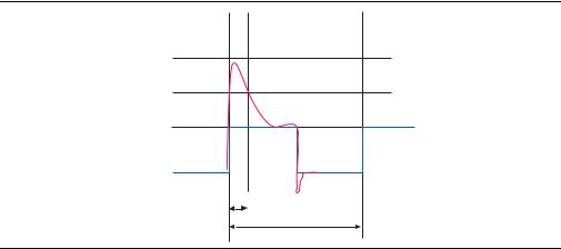
(1)Figure 1–1 shows the methodology to determine the overshoot duration. In the example in Figure 1–1, overshoot voltage is shown in red and is present on the input pin of the Cyclone III device at over 4.1 V but below 4.2 V. From Table 1–1, for an overshoot of 4.1 V, the percentage of high time for the overshoot can be as high as 31.97% over a 10-year period. Percentage of high time is calculated as ([delta T]/T) × 100. This 10-year period assumes the device is always turned on with 100% I/O toggle rate and 50% duty cycle signal. For lower I/O toggle rates and situations in which the device is in an idle state, lifetimes are increased.
Figure 1–1 shows the methodology to determine the overshoot duration.
Figure 1–1. Cyclone III Devices Overshoot Duration
4.2 V
4.1 V
3.3 V
T
T
July 2012 Altera Corporation |
Cyclone III Device Handbook |
|
Volume 2 |
1–4 |
Chapter 1: Cyclone III Device Datasheet |
|
Electrical Characteristics |
|
|
Recommended Operating Conditions
This section lists the functional operation limits for AC and DC parameters for Cyclone III devices. The steady-state voltage and current values expected from Cyclone III devices are provided in Table 1–3. All supplies must be strictly monotonic without plateaus.
Table 1–3. Cyclone III Devices Recommended Operating Conditions (1), (2)
Symbol |
Parameter |
Conditions |
Min |
Typ |
Max |
Unit |
||
|
|
|
|
|
|
|
|
|
VCCINT |
(3) |
Supply voltage for internal logic |
— |
1.15 |
1.2 |
1.25 |
V |
|
|
|
Supply voltage for output buffers, 3.3-V |
— |
3.135 |
3.3 |
3.465 |
V |
|
|
|
operation |
||||||
|
|
|
|
|
|
|
||
|
|
|
|
|
|
|
|
|
|
|
Supply voltage for output buffers, 3.0-V |
— |
2.85 |
3 |
3.15 |
V |
|
|
|
operation |
||||||
|
|
|
|
|
|
|
||
|
|
|
|
|
|
|
|
|
|
|
Supply voltage for output buffers, 2.5-V |
— |
2.375 |
2.5 |
2.625 |
V |
|
|
|
operation |
||||||
VCCIO |
(3), (4) |
|
|
|
|
|
||
|
|
|
|
|
|
|||
Supply voltage for output buffers, 1.8-V |
— |
1.71 |
1.8 |
1.89 |
V |
|||
|
|
|||||||
|
|
operation |
||||||
|
|
|
|
|
|
|
||
|
|
|
|
|
|
|
|
|
|
|
Supply voltage for output buffers, 1.5-V |
— |
1.425 |
1.5 |
1.575 |
V |
|
|
|
operation |
||||||
|
|
|
|
|
|
|
||
|
|
|
|
|
|
|
|
|
|
|
Supply voltage for output buffers, 1.2-V |
— |
1.14 |
1.2 |
1.26 |
V |
|
|
|
operation |
||||||
|
|
|
|
|
|
|
||
|
|
|
|
|
|
|
|
|
VCCA (3) |
Supply (analog) voltage for PLL |
— |
2.375 |
2.5 |
2.625 |
V |
||
regulator |
||||||||
|
|
|
|
|
|
|
||
|
|
|
|
|
|
|
||
VCCD_PLL (3) |
Supply (digital) voltage for PLL |
— |
1.15 |
1.2 |
1.25 |
V |
||
VI |
|
Input voltage |
— |
–0.5 |
— |
3.6 |
V |
|
VO |
|
Output voltage |
— |
0 |
— |
VCCIO |
V |
|
|
|
|
For commercial use |
0 |
— |
85 |
°C |
|
|
|
|
|
|
|
|
|
|
TJ |
|
Operating junction temperature |
For industrial use |
–40 |
— |
100 |
°C |
|
|
|
|
|
|
|
|||
|
For extended temperature |
–40 |
— |
125 |
°C |
|||
|
|
|
||||||
|
|
|
|
|
|
|
|
|
|
|
|
For automotive use |
–40 |
— |
125 |
°C |
|
|
|
|
|
|
|
|
|
|
|
|
|
Standard power-on reset |
50 µs |
— |
50 ms |
— |
|
tRAMP |
|
Power supply ramp time |
(POR) (5) |
|||||
|
|
|
|
|
||||
|
|
|
Fast POR (6) |
50 µs |
— |
3 ms |
— |
|
IDiode |
|
Magnitude of DC current across |
— |
— |
— |
10 |
mA |
|
|
PCI-clamp diode when enabled |
|||||||
|
|
|
|
|
|
|
||
|
|
|
|
|
|
|
|
|
Notes to Table 1–3:
(1)VCCIO for all I/O banks must be powered up during device operation. All VCCA pins must be powered to 2.5 V (even when PLLs are not used), and must be powered up and powered down at the same time.
(2)VCCD_PLL must always be connected to VCCINT through a decoupling capacitor and ferrite bead.
(3)The VCC must rise monotonically.
(4)All input buffers are powered by the VCCIO supply.
(5)POR time for Standard POR ranges between 50–200 ms. Each individual power supply should reach the recommended operating range within 50 ms.
(6)POR time for Fast POR ranges between 3–9 ms. Each individual power supply should reach the recommended operating range within 3 ms.
Cyclone III Device Handbook |
July 2012 Altera Corporation |
Volume 2 |
|

Chapter 1: Cyclone III Device Datasheet |
1–5 |
Electrical Characteristics
DC Characteristics
This section lists the I/O leakage current, pin capacitance, on-chip termination (OCT) tolerance, and bus hold specifications for Cyclone III devices.
Supply Current
Standby current is the current the device draws after the device is configured with no inputs or outputs toggling and no activity in the device. Use the Excel-based early power estimator (EPE) to get the supply current estimates for your design because these currents vary largely with the resources used. Table 1–4 lists I/O pin leakage current for Cyclone III devices.
fFor more information about power estimation tools, refer to the PowerPlay Early Power Estimator User Guide and the PowerPlay Power Analysis chapter in the Quartus II Handbook.
Table 1–4. Cyclone III Devices I/O Pin Leakage Current (1), (2)
Symbol |
Parameter |
Conditions |
Min |
Typ |
Max |
Unit |
|
|
|
|
|
|
|
|
|
II |
Input pin leakage current |
VI = 0 V to VCCIOMAX |
–10 |
— |
10 |
A |
|
IOZ |
Tristated I/O pin leakage |
VO = 0 V to VCCIOMAX |
–10 |
— |
10 |
A |
|
current |
|||||||
|
|
|
|
|
|
||
|
|
|
|
|
|
|
Notes to Table 1–4:
(1)This value is specified for normal device operation. The value varies during device power-up. This applies for all VCCIO settings (3.3, 3.0, 2.5, 1.8, 1.5, and 1.2 V).
(2)10 A I/O leakage current limit is applicable when the internal clamping diode is off. A higher current can be the observed when the diode is on.
Bus Hold
Bus hold retains the last valid logic state after the source driving it either enters the high impedance state or is removed. Each I/O pin has an option to enable bus hold in user mode. Bus hold is always disabled in configuration mode.
Table 1–5 lists bus hold specifications for Cyclone III devices.
Table 1–5. Cyclone III Devices Bus Hold Parameter |
|
(Part 1 of 2) |
(1) |
|
|
|
|
|
|
|
|
|||||||
|
|
|
|
|
|
|
|
|
|
VCCIO (V) |
|
|
|
|
|
|
|
|
Parameter |
Condition |
|
|
|
|
|
|
|
|
|
|
|
|
|
|
|
|
|
|
1.2 |
|
1.5 |
|
1.8 |
|
2.5 |
3.0 |
3.3 |
Unit |
||||||||
|
|
|
|
|
|
|
|
|
|
|
|
|
|
|
|
|
|
|
|
|
Min |
|
Max |
Min |
|
Max |
Min |
|
Max |
Min |
|
Max |
Min |
Max |
Min |
Max |
|
|
|
|
|
|
|
|
|
|
|
|
|
|
|
|
|
|
|
|
Bus-hold |
VIN > VIL |
|
|
|
|
|
|
|
|
|
|
|
|
|
|
|
|
|
low, |
8 |
|
— |
12 |
|
— |
30 |
|
— |
50 |
|
— |
70 |
— |
70 |
— |
A |
|
sustaining |
(maximum) |
|
|
|
|
|||||||||||||
|
|
|
|
|
|
|
|
|
|
|
|
|
|
|
|
|
||
current |
|
|
|
|
|
|
|
|
|
|
|
|
|
|
|
|
|
|
|
|
|
|
|
|
|
|
|
|
|
|
|
|
|
|
|
|
|
Bus-hold |
VIN < VIL |
|
|
|
|
|
|
|
|
|
|
|
|
|
|
|
|
|
high, |
–8 |
|
— |
–12 |
|
— |
–30 |
|
— |
–50 |
|
— |
–70 |
— |
–70 |
— |
A |
|
sustaining |
(minimum) |
|
|
|
|
|||||||||||||
|
|
|
|
|
|
|
|
|
|
|
|
|
|
|
|
|
||
current |
|
|
|
|
|
|
|
|
|
|
|
|
|
|
|
|
|
|
|
|
|
|
|
|
|
|
|
|
|
|
|
|
|
|
|
|
|
July 2012 Altera Corporation |
Cyclone III Device Handbook |
|
Volume 2 |
1–6 |
Chapter 1: Cyclone III Device Datasheet |
|
Electrical Characteristics |
|
|
Table 1–5. Cyclone III Devices Bus Hold Parameter |
(Part 2 of 2) |
(1) |
|
|
|
|
|
|
|
|
||||||||
|
|
|
|
|
|
|
|
|
|
VCCIO (V) |
|
|
|
|
|
|
|
|
Parameter |
Condition |
|
|
|
|
|
|
|
|
|
|
|
|
|
|
|||
|
1.2 |
1.5 |
1.8 |
|
2.5 |
3.0 |
3.3 |
Unit |
||||||||||
|
|
|
|
|
|
|
|
|
|
|
|
|
|
|
|
|
|
|
|
|
|
Min |
|
Max |
Min |
Max |
Min |
|
Max |
Min |
|
Max |
Min |
Max |
Min |
Max |
|
|
|
|
|
|
|
|
|
|
|
|
|
|
|
|
|
|
|
|
Bus-hold |
|
|
|
|
|
|
|
|
|
|
|
|
|
|
|
|
|
|
low, |
0 V < VIN |
< VCCIO |
— |
|
125 |
— |
175 |
— |
|
200 |
— |
|
300 |
— |
500 |
— |
500 |
A |
overdrive |
|
|
|
|||||||||||||||
|
|
|
|
|
|
|
|
|
|
|
|
|
|
|
|
|
|
|
current |
|
|
|
|
|
|
|
|
|
|
|
|
|
|
|
|
|
|
|
|
|
|
|
|
|
|
|
|
|
|
|
|
|
|
|
|
|
Bus-hold |
|
|
|
|
|
|
|
|
|
|
|
|
|
|
|
|
|
|
high, |
0 V < VIN |
< VCCIO |
— |
|
–125 |
— |
–175 |
— |
|
–200 |
— |
|
–300 |
— |
–500 |
— |
–500 |
A |
overdrive |
|
|
|
|||||||||||||||
|
|
|
|
|
|
|
|
|
|
|
|
|
|
|
|
|
|
|
current |
|
|
|
|
|
|
|
|
|
|
|
|
|
|
|
|
|
|
|
|
|
|
|
|
|
|
|
|
|
|
|
|
|
|
|
|
|
Bus-hold trip |
— |
|
0.3 |
|
0.9 |
0.375 |
1.125 |
0.68 |
|
1.07 |
0.7 |
|
1.7 |
0.8 |
2 |
0.8 |
2 |
V |
point |
|
|
|
|
||||||||||||||
|
|
|
|
|
|
|
|
|
|
|
|
|
|
|
|
|
|
|
|
|
|
|
|
|
|
|
|
|
|
|
|
|
|
|
|
|
|
Note to Table 1–5: |
|
|
|
|
|
|
|
|
|
|
|
|
|
|
|
|
|
|
(1) The bus-hold trip points are based on calculated input voltages from the JEDEC standard.
OCT Specifications
Table 1–6 lists the variation of OCT without calibration across process, temperature, and voltage.
Table 1–6. Cyclone III Devices Series OCT without Calibration Specifications
|
|
Resistance Tolerance |
|
||
Description |
VCCIO (V) |
|
|
Unit |
|
Commercial |
Industrial and Automotive |
||||
|
|
Max |
Max |
|
|
|
|
|
|
|
|
|
3.0 |
±30 |
±40 |
% |
|
|
|
|
|
|
|
Series OCT without |
2.5 |
±30 |
±40 |
% |
|
|
|
|
|
||
1.8 |
+40 |
±50 |
% |
||
calibration |
|||||
|
|
|
|
||
1.5 |
+50 |
±50 |
% |
||
|
|||||
|
|
|
|
|
|
|
1.2 |
+50 |
±50 |
% |
|
|
|
|
|
|
|
OCT calibration is automatically performed at device power-up for OCT enabled
I/Os.
Table 1–7 lists the OCT calibration accuracy at device power-up.
Table 1–7. Cyclone III Devices Series OCT with Calibration at Device Power-Up Specifications
|
|
|
Calibration Accuracy |
|
|
Description |
VCCIO (V) |
|
|
|
Unit |
Commercial Max |
Industrial and Automotive |
||||
|
|
Max |
|
||
|
|
|
|
|
|
|
|
|
|
|
|
|
3.0 |
±10 |
|
±10 |
% |
|
|
|
|
|
|
Series OCT with |
2.5 |
±10 |
|
±10 |
% |
|
|
|
|
|
|
calibration at device |
1.8 |
±10 |
|
±10 |
% |
power-up |
|
|
|
|
|
1.5 |
±10 |
|
±10 |
% |
|
|
|
||||
|
|
|
|
|
|
|
1.2 |
±10 |
|
±10 |
% |
|
|
|
|
|
|
Cyclone III Device Handbook |
July 2012 Altera Corporation |
Volume 2 |
|

Chapter 1: Cyclone III Device Datasheet |
1–7 |
Electrical Characteristics |
|
|
|
The OCT resistance may vary with the variation of temperature and voltage after calibration at device power-up. Use Table 1–8 and Equation 1–1 to determine the final OCT resistance considering the variations after calibration at device power-up. Table 1–8 lists the change percentage of the OCT resistance with voltage and temperature.
Table 1–8. Cyclone III Devices OCT Variation After Calibration at Device Power-Up
Nominal Voltage |
dR/dT (%/°C) |
dR/dV (%/mV) |
|
|
|
3.0 |
0.262 |
–0.026 |
|
|
|
2.5 |
0.234 |
–0.039 |
|
|
|
1.8 |
0.219 |
–0.086 |
|
|
|
1.5 |
0.199 |
–0.136 |
|
|
|
1.2 |
0.161 |
–0.288 |
|
|
|
Equation 1–1. (1), (2), (3), (4), (5), (6)
RV = (V2 – V1) × 1000 × dR/dV (7)RT = (T2 – T1) × dR/dT (8)
For Rx < 0; MFx = 1/ (| Rx|/100 + 1) (9)
For Rx > 0; MFx = Rx/100 + 1 (10)
MF = MFV × MFT (11)
Rfinal = Rinitial × MF (12)
Notes to Equation 1–1:
(1)T2 is the final temperature.
(2)T1 is the initial temperature.
(3)MF is multiplication factor.
(4)Rfinal is final resistance.
(5)Rinitial is initial resistance.
(6)Subscript × refers to both V and T.
(7)RV is variation of resistance with voltage.
(8)RT is variation of resistance with temperature.
(9)dR/dT is the change percentage of resistance with temperature after calibration at device power-up.
(10)dR/dV is the change percentage of resistance with voltage after calibration at device power-up.
(11)V2 is final voltage.
(12)V1 is the initial voltage.
July 2012 Altera Corporation |
Cyclone III Device Handbook |
|
Volume 2 |

1–8 |
Chapter 1: Cyclone III Device Datasheet |
|
Electrical Characteristics |
|
|
Example 1–1 shows you the example to calculate the change of 50 I/O impedance from 25°C at 3.0 V to 85°C at 3.15 V:
Example 1–1.
RV = (3.15 – 3) × 1000 × –0.026 = –3.83
RT = (85 – 25) × 0.262 = 15.72 Because RV is negative,
MFV = 1 / (3.83/100 + 1) = 0.963 Because RT is positive,
MFT = 15.72/100 + 1 = 1.157
MF = 0.963 × 1.157 = 1.114
Rfinal = 50 × 1.114 = 55.71
Pin Capacitance
Table 1–9 lists the pin capacitance for Cyclone III devices.
Table 1–9. Cyclone III Devices Pin Capacitance
Symbol |
Parameter |
Typical – |
Typical – |
Unit |
|
QFP |
FBGA |
||||
|
|
|
|||
|
|
|
|
|
|
CIOTB |
Input capacitance on top/bottom I/O pins |
7 |
6 |
pF |
|
CIOLR |
Input capacitance on left/right I/O pins |
7 |
5 |
pF |
|
CLVDSLR |
Input capacitance on left/right I/O pins with dedicated |
8 |
7 |
pF |
|
LVDS output |
|||||
|
|
|
|
||
|
|
|
|
|
|
CVREFLR |
Input capacitance on left/right dual-purpose VREF pin |
21 |
21 |
pF |
|
(1) |
when used as VREF or user I/O pin |
||||
|
|
|
|||
|
|
|
|
||
CVREFTB |
Input capacitance on top/bottom dual-purpose VREF pin |
23 (2) |
23 (2) |
pF |
|
(1) |
when used as VREF or user I/O pin |
|
|
|
|
|
|
|
|
||
CCLKTB |
Input capacitance on top/bottom dedicated clock input |
7 |
6 |
pF |
|
pins |
|||||
|
|
|
|
||
|
|
|
|
|
|
CCLKLR |
Input capacitance on left/right dedicated clock input pins |
6 |
5 |
pF |
Notes to Table 1–9:
(1)When VREF pin is used as regular input or output, a reduced performance of toggle rate and tCO is expected due to higher pin capacitance.
(2)CVREFTB for EP3C25 is 30 pF.
Cyclone III Device Handbook |
July 2012 Altera Corporation |
Volume 2 |
|
Chapter 1: Cyclone III Device Datasheet |
1–9 |
Electrical Characteristics |
|
|
|
Internal Weak Pull-Up and Weak Pull-Down Resistor
Table 1–10 lists the weak pull-up and pull-down resistor values for Cyclone III devices.
Table 1–10. |
Cyclone III Devices Internal Weak Pull-Up and Weak Pull-Down Resistor |
(1) |
|
|
|
|||||
|
|
|
|
|
|
|
|
|
|
|
Symbol |
Parameter |
|
|
Conditions |
|
Min |
Typ |
Max |
Unit |
|
|
|
|
|
|
|
|
|
|
||
|
|
VCCIO = 3.3 V ± 5% |
(2), |
(3) |
7 |
25 |
41 |
k |
||
|
Value of I/O pin pull-up resistor before |
VCCIO = 3.0 V ± 5% |
(2), |
(3) |
7 |
28 |
47 |
k |
||
|
VCCIO = 2.5 V ± 5% |
(2), |
(3) |
8 |
35 |
61 |
k |
|||
R_PU |
and during configuration, as well as |
|||||||||
user mode if the programmable |
VCCIO = 1.8 V ± 5% |
(2), |
(3) |
10 |
57 |
108 |
k |
|||
|
pull-up resistor option is enabled |
|
|
|
|
|
|
|
|
|
|
VCCIO = 1.5 V ± 5% |
(2), |
(3) |
13 |
82 |
163 |
k |
|||
|
|
|||||||||
|
|
VCCIO = 1.2 V ± 5% |
(2), |
(3) |
19 |
143 |
351 |
k |
||
|
|
VCCIO = 3.3 V ± 5% |
(4) |
|
6 |
19 |
30 |
k |
||
|
Value of I/O pin pull-down resistor |
VCCIO = 3.0 V ± 5% |
(4) |
|
6 |
22 |
36 |
k |
||
R |
V |
CCIO |
= 2.5 V ± 5% |
(4) |
|
6 |
25 |
43 |
k |
|
|
|
|||||||||
_PD |
before and during configuration |
|
|
|
|
|
|
|
|
|
|
VCCIO = 1.8 V ± 5% |
(4) |
|
7 |
35 |
71 |
k |
|||
|
|
|
||||||||
|
|
VCCIO = 1.5 V ± 5% |
(4) |
|
8 |
50 |
112 |
k |
||
Notes to Table 1–10:
(1)All I/O pins have an option to enable weak pull-up except configuration, test, and JTAG pin. Weak pull-down feature is only available for JTAG TCK.
(2)Pin pull-up resistance values may be lower if an external source drives the pin higher than VCCIO.
(3)R_PU = (VCCIO – VI)/IR_PU
Minimum condition: –40°C; VCCIO = VCC + 5%, VI = VCC + 5% – 50 mV; Typical condition: 25°C; VCCIO = VCC, VI = 0 V;
Maximum condition: 125°C; VCCIO = VCC – 5%, VI = 0 V; in which VI refers to the input voltage at the I/O pin.
(4)R_PD = VI/IR_PD
Minimum condition: –40°C; VCCIO = VCC + 5%, VI = 50 mV; Typical condition: 25°C; VCCIO = VCC, VI = VCC – 5%;
Maximum condition: 125°C; VCCIO = VCC – 5%, VI = VCC – 5%; in which VI refers to the input voltage at the I/O pin.
Hot Socketing
Table 1–11 lists the hot-socketing specifications for Cyclone III devices.
Table 1–11. Cyclone III Devices Hot-Socketing Specifications
Symbol |
Parameter |
Maximum |
|
|
|
IIOPIN(DC) |
DC current per I/O pin |
300 A |
IIOPIN(AC) |
AC current per I/O pin |
8 mA (1) |
Note to Table 1–11:
(1)The I/O ramp rate is 10 ns or more. For ramp rates faster than 10 ns, |IIOPIN| = C dv/dt, in which C is I/O pin capacitance and dv/dt is the slew rate.
July 2012 Altera Corporation |
Cyclone III Device Handbook |
|
Volume 2 |
1–10 |
Chapter 1: Cyclone III Device Datasheet |
|
Electrical Characteristics |
|
|
Schmitt Trigger Input
Cyclone III devices support Schmitt trigger input on TDI, TMS, TCK, nSTATUS, nCONFIG, nCE, CONF_DONE, and DCLK pins. A Schmitt trigger feature introduces hysteresis to the input signal for improved noise immunity, especially for signal with slow edge rate. Table 1–12 lists the hysteresis specifications across supported VCCIO range for Schmitt trigger inputs in Cyclone III devices.
Table 1–12. Hysteresis Specifications for Schmitt Trigger Input in Cyclone III Devices
Symbol |
Parameter |
Conditions |
Minimum |
Typical |
Maximum |
Unit |
|
|
|
|
|
|
|
|
|
|
|
VCCIO = 3.3 V |
200 |
— |
— |
mV |
|
VSCHMITT |
Hysteresis for Schmitt trigger |
VCCIO = 2.5 V |
200 |
— |
— |
mV |
|
input |
VCCIO = 1.8 V |
140 |
— |
— |
mV |
||
|
|||||||
|
|
VCCIO = 1.5 V |
110 |
— |
— |
mV |
I/O Standard Specifications
The following tables list input voltage sensitivities (VIH and VIL), output voltage (VOH and VOL), and current drive characteristics (IOH and IOL) for various I/O standards supported by Cyclone III devices. Table 1–13 through Table 1–18 provide the I/O standard specifications for Cyclone III devices.
Table 1–13. Cyclone III Devices Single-Ended I/O Standard Specifications (1), (2)
I/O Standard |
|
VCCIO (V) |
|
VIL (V) |
|
VIH (V) |
VOL (V) |
VOH (V) |
IOL |
IOH |
|||
|
|
|
|
|
|
|
|
|
|
|
|||
|
Min |
Typ |
|
Max |
Min |
Max |
Min |
|
Max |
Max |
Min |
(mA) |
(mA) |
|
|
|
|
|
|||||||||
|
|
|
|
|
|
|
|
|
|
|
|
|
|
3.3-V LVTTL (3) |
3.135 |
3.3 |
|
3.465 |
— |
0.8 |
1.7 |
|
3.6 |
0.45 |
2.4 |
4 |
–4 |
3.3-V LVCMOS (3) |
3.135 |
3.3 |
|
3.465 |
— |
0.8 |
1.7 |
|
3.6 |
0.2 |
VCCIO – 0.2 |
2 |
–2 |
3.0-V LVTTL (3) |
2.85 |
3.0 |
|
3.15 |
–0.3 |
0.8 |
1.7 |
|
VCCIO + 0.3 |
0.45 |
2.4 |
4 |
–4 |
3.0-V LVCMOS (3) |
2.85 |
3.0 |
|
3.15 |
–0.3 |
0.8 |
1.7 |
|
VCCIO + 0.3 |
0.2 |
VCCIO – 0.2 |
0.1 |
–0.1 |
2.5-V LVTTL and |
2.375 |
2.5 |
|
2.625 |
–0.3 |
0.7 |
1.7 |
|
3.6 |
0.4 |
2.0 |
1 |
–1 |
LVCMOS (3) |
|
|
|||||||||||
|
|
|
|
|
|
|
|
|
|
|
|
|
|
1.8-V LVTTL and |
1.71 |
1.8 |
|
1.89 |
–0.3 |
0.35 * |
0.65 * |
|
2.25 |
0.45 |
VCCIO – |
2 |
–2 |
LVCMOS |
|
VCCIO |
VCCIO |
|
0.45 |
||||||||
|
|
|
|
|
|
|
|
|
|
||||
1.5-V LVCMOS |
1.425 |
1.5 |
|
1.575 |
–0.3 |
0.35 * |
0.65 * |
|
VCCIO + 0.3 |
0.25 * |
0.75 * |
2 |
–2 |
|
VCCIO |
VCCIO |
|
VCCIO |
VCCIO |
||||||||
|
|
|
|
|
|
|
|
|
|
||||
1.2-V LVCMOS |
1.14 |
1.2 |
|
1.26 |
–0.3 |
0.35 * |
0.65 * |
|
VCCIO + 0.3 |
0.25 * |
0.75 * |
2 |
–2 |
|
VCCIO |
VCCIO |
|
VCCIO |
VCCIO |
||||||||
|
|
|
|
|
|
|
|
|
|
||||
3.0-V PCI |
2.85 |
3.0 |
|
3.15 |
— |
0.3 * |
0.5 * |
|
VCCIO + 0.3 |
0.1 * VCCIO |
0.9 * VCCIO |
1.5 |
–0.5 |
|
VCCIO |
VCCIO |
|
||||||||||
|
|
|
|
|
|
|
|
|
|
|
|
||
3.0-V PCI-X |
2.85 |
3.0 |
|
3.15 |
— |
0.35* |
0.5 * |
|
VCCIO + 0.3 |
0.1 * VCCIO |
0.9 * VCCIO |
1.5 |
–0.5 |
|
VCCIO |
VCCIO |
|
||||||||||
|
|
|
|
|
|
|
|
|
|
|
|
||
Notes to Table 1–13:
(1)For voltage referenced receiver input waveform and explanation of terms used in Table 1–13, refer to “Single-ended Voltage referenced I/O Standard” in “Glossary” on page 1–27.
(2)AC load CL = 10 pF.
(3)For more detail about interfacing Cyclone III devices with 3.3/3.0/2.5-V LVTTL/LVCMOS I/O standards, refer to AN 447: Interfacing Cyclone III Devices with 3.3/3.0/2.5-V LVTTL and LVCMOS I/O Systems.
Cyclone III Device Handbook |
July 2012 Altera Corporation |
Volume 2 |
|
Chapter 1: Cyclone III Device Datasheet |
1–11 |
Electrical Characteristics |
|
|
|
Table 1–14. Cyclone III Devices Single-Ended SSTL and HSTL I/O Reference Voltage Specifications |
(1) |
|
|
|
|||||||||||||||
I/O |
V |
CCIO |
(V) |
|
|
|
V |
REF |
(V) |
|
|
|
|
V |
TT |
(V) (2) |
|
||
|
|
|
|
|
|
|
|
|
|
|
|
|
|
|
|
||||
Standard |
Min |
|
Typ |
|
Max |
Min |
|
|
Typ |
|
Max |
|
Min |
|
Typ |
Max |
|||
|
|
|
|
|
|
|
|
||||||||||||
|
|
|
|
|
|
|
|
|
|
|
|
|
|
|
|
|
|
|
|
SSTL-2 |
2.375 |
|
2.5 |
|
2.625 |
1.19 |
|
|
1.25 |
|
1.31 |
|
VREF – |
|
VREF |
VREF + |
|||
Class I, II |
|
|
|
|
|
|
0.04 |
|
0.04 |
||||||||||
|
|
|
|
|
|
|
|
|
|
|
|
|
|
|
|
|
|||
|
|
|
|
|
|
|
|
|
|
|
|
|
|
|
|
|
|
|
|
SSTL-18 |
1.7 |
|
1.8 |
|
1.9 |
0.833 |
|
|
0.9 |
|
0.969 |
|
VREF – |
|
VREF |
VREF + |
|||
Class I, II |
|
|
|
|
|
|
0.04 |
|
0.04 |
||||||||||
|
|
|
|
|
|
|
|
|
|
|
|
|
|
|
|
|
|||
|
|
|
|
|
|
|
|
|
|
|
|
|
|
|
|
|
|
|
|
HSTL-18 |
1.71 |
|
1.8 |
|
1.89 |
0.85 |
|
|
0.9 |
|
0.95 |
|
0.85 |
|
0.9 |
0.95 |
|||
Class I, II |
|
|
|
|
|
|
|
||||||||||||
|
|
|
|
|
|
|
|
|
|
|
|
|
|
|
|
|
|
|
|
|
|
|
|
|
|
|
|
|
|
|
|
|
|
|
|
|
|
|
|
HSTL-15 |
1.425 |
|
1.5 |
|
1.575 |
0.71 |
|
|
0.75 |
|
0.79 |
|
0.71 |
|
0.75 |
0.79 |
|||
Class I, II |
|
|
|
|
|
|
|
||||||||||||
|
|
|
|
|
|
|
|
|
|
|
|
|
|
|
|
|
|
|
|
|
|
|
|
|
|
|
|
|
|
|
|
|
|
|
|
||||
HSTL-12 |
1.14 |
|
1.2 |
|
1.26 |
0.48 * VCCIO |
(3) |
0.5 * VCCIO |
(3) |
0.52 * VCCIO |
(3) |
— |
0.5 * |
— |
|||||
Class I, II |
|
|
0.47 * VCCIO |
(4) |
0.5 * VCCIO |
(4) |
0.53 * VCCIO |
(4) |
VCCIO |
||||||||||
|
|
|
|
|
|
|
|
||||||||||||
Notes to Table 1–14:
(1)For an explanation of terms used in Table 1–14, refer to “Glossary” on page 1–27.
(2)VTT of transmitting device must track VREF of the receiving device.
(3)Value shown refers to DC input reference voltage, VREF(DC).
(4)Value shown refers to AC input reference voltage, VREF(AC).
Table 1–15. Cyclone III Devices Single-Ended SSTL and HSTL I/O Standards Signal Specifications
I/O |
VIL(DC) (V) |
|
VIH(DC) (V) |
|
VIL(AC) (V) |
|
VIH(AC) (V) |
VOL (V) |
VOH (V) |
IOL |
IOH |
||||||
Standard |
Min |
Max |
Min |
Max |
Min |
Max |
Min |
Max |
Max |
Min |
|
(mA) |
(mA) |
||||
|
|
|
|
||||||||||||||
|
|
|
|
|
|
|
|
|
|
|
|
|
|
|
|
||
SSTL-2 |
— |
VREF – |
VREF |
+ |
— |
— |
VREF – |
VREF |
+ |
— |
VTT – |
VTT + |
8.1 |
–8.1 |
|||
Class I |
0.18 |
0.18 |
0.35 |
0.35 |
0.57 |
0.57 |
|||||||||||
|
|
|
|
|
|
|
|||||||||||
|
|
|
|
|
|
|
|
|
|
|
|
|
|
|
|
||
SSTL-2 |
— |
VREF – |
VREF |
+ |
— |
— |
VREF – |
VREF |
+ |
— |
VTT – |
VTT + |
16.4 |
–16.4 |
|||
Class II |
0.18 |
0.18 |
0.35 |
0.35 |
0.76 |
0.76 |
|||||||||||
|
|
|
|
|
|
|
|||||||||||
|
|
|
|
|
|
|
|
|
|
|
|
|
|
|
|
||
SSTL-18 |
— |
VREF – |
VREF |
+ |
— |
— |
VREF – |
VREF |
+ |
— |
VTT – |
VTT + |
6.7 |
–6.7 |
|||
Class I |
0.125 |
0.125 |
0.25 |
0.25 |
0.475 |
0.475 |
|||||||||||
|
|
|
|
|
|
|
|||||||||||
|
|
|
|
|
|
|
|
|
|
|
|
|
|
|
|
|
|
SSTL-18 |
— |
VREF – |
VREF |
+ |
— |
— |
VREF – |
VREF |
+ |
— |
0.28 |
VCCIO |
– |
13.4 |
–13.4 |
||
Class II |
0.125 |
0.125 |
0.25 |
0.25 |
0.28 |
||||||||||||
|
|
|
|
|
|
|
|
||||||||||
|
|
|
|
|
|
|
|
|
|
|
|
|
|
|
|
|
|
HSTL-18 |
— |
VREF – |
VREF |
+ |
— |
— |
VREF – |
VREF |
+ |
— |
0.4 |
VCCIO |
– |
8 |
–8 |
||
Class I |
0.1 |
0.1 |
|
0.2 |
0.2 |
|
0.4 |
|
|||||||||
|
|
|
|
|
|
|
|
|
|
|
|||||||
|
|
|
|
|
|
|
|
|
|
|
|
|
|
|
|
|
|
HSTL-18 |
— |
VREF – |
VREF |
+ |
— |
— |
VREF – |
VREF |
+ |
— |
0.4 |
VCCIO |
– |
16 |
–16 |
||
Class II |
0.1 |
0.1 |
|
0.2 |
0.2 |
|
0.4 |
|
|||||||||
|
|
|
|
|
|
|
|
|
|
|
|||||||
|
|
|
|
|
|
|
|
|
|
|
|
|
|
|
|
|
|
HSTL-15 |
— |
VREF – |
VREF |
+ |
— |
— |
VREF – |
VREF |
+ |
— |
0.4 |
VCCIO |
– |
8 |
–8 |
||
Class I |
0.1 |
0.1 |
|
0.2 |
0.2 |
|
0.4 |
|
|||||||||
|
|
|
|
|
|
|
|
|
|
|
|||||||
|
|
|
|
|
|
|
|
|
|
|
|
|
|
|
|
|
|
HSTL-15 |
— |
VREF – |
VREF |
+ |
— |
— |
VREF – |
VREF |
+ |
— |
0.4 |
VCCIO |
– |
16 |
–16 |
||
Class II |
0.1 |
0.1 |
|
0.2 |
0.2 |
|
0.4 |
|
|||||||||
|
|
|
|
|
|
|
|
|
|
|
|||||||
|
|
|
|
|
|
|
|
|
|
|
|
|
|
|
|||
HSTL-12 |
–0.15 |
VREF – |
VREF |
+ |
VCCIO |
+ 0.15 |
–0.24 |
VREF – |
VREF + |
VCCIO + |
0.25 × |
0.75 × |
8 |
–8 |
|||
Class I |
0.08 |
0.08 |
0.15 |
0.15 |
0.24 |
VCCIO |
VCCIO |
||||||||||
|
|
|
|
|
|
||||||||||||
HSTL-12 |
–0.15 |
VREF – |
VREF |
+ |
VCCIO |
+ 0.15 |
–0.24 |
VREF – |
VREF + |
VCCIO + |
0.25 × |
0.75 × |
14 |
–14 |
|||
Class II |
0.08 |
0.08 |
0.15 |
0.15 |
0.24 |
VCCIO |
VCCIO |
||||||||||
|
|
|
|
|
|
||||||||||||
July 2012 Altera Corporation |
Cyclone III Device Handbook |
|
Volume 2 |
Loading...