


 Loading...
Altera LVDS SERDES IP Core User Guide
2014.08.18
ug_altera_lvds |
Subscribe |
Send Feedback |
The Altera LVDS SERDES IP Core configures the serializer/deserializer (SERDES) and dynamic phase alignment (DPA) blocks. The IP core also supports LVDS channels placement, legality checks, and LVDS channel-related rule checks.
The Altera LVDS SERDES IP core is only available for Arria® 10 devices. For Arria V, Cyclone® V, and Stratix® V devices, follow the steps in Migrating Your ALTLVDS_TX and ALTLVDS_RX IP Cores on page 25 to migrate your IP.
Related Information
• LVDS SERDES Transmitter/Receiver (ALTLVDS_TX and ALTLVDS_RX) Megafunctions User Guide
Features
You can configure the features of Altera LVDS SERDES IP core through the IP Parameter Editor in the Quartus® II software. The Altera LVDS SERDES IP core feature includes the ALTLVDS_RX and ALTLVDS_TX IP cores features supported in Stratix V devices, such as:
•Parameterizable data channel widths
•Parameterizable serializer/deserializer (SERDES) factors
•Registered input and output ports
•PLL control signals
•Dynamic phase alignment (DPA) mode
•Soft clock data recovery (CDR) mode
Functional Modes
This table lists the functional modes for the Altera LVDS SERDES IP core.
Table 1: Functional Modes for the Altera LVDS SERDES IP Core
Functional Mode |
Description |
TX |
In this mode, the IP core configures the SERDES block as a serializer. A |
|
PLL generates the fast clock (fclk) and load enable (loaden) signals. |
© 2014 Altera Corporation. All rights reserved. ALTERA, ARRIA, CYCLONE, ENPIRION, MAX, MEGACORE, NIOS, QUARTUS and STRATIX words and logos are trademarks of Altera Corporation and registered in the U.S. Patent and Trademark Office and in other countries. All other words and logos identified as trademarks or service marks are the property of their respective holders as described at www.altera.com/common/legal.html. Altera warrants performance of its semiconductor products to current specifications in accordance with Altera's standard warranty, but reserves the right to make changes to any products and services at any time without notice. Altera assumes no responsibility or liability arising out of the application or use of any information, product, or service described herein except as expressly agreed to in writing by Altera. Altera customers are advised to obtain the latest version of device specifications before relying on any published information and before placing orders for products or services.
ISO 9001:2008 Registered
101 Innovation Drive, San Jose, CA 95134

2Functional Description
Functional Mode
RX Non-DPA Mode
ug_altera_lvds 2014.08.18
Description
In this mode, you must ensure the correct clock-data alignment, as the incoming data is captured at the bitslip with the fclk signal. The DPA and DPA-FIFO are bypassed. As in the transmitter mode, the fclk signal is provided by a PLL.
RX DPA-FIFO |
In this mode, the DPA block selects an optimal phase to sample incoming |
|
data from a set of eight DPA clocks running at the fclk frequency, each 45° |
|
out of phase. The DPA-FIFO, a circular buffer, samples the incoming data |
|
with the selected DPA clock and forwards the data to LVDS clock domain. |
|
The data released from the DPA-FIFO is then sampled at the bitslip circuitry, |
|
where it is lagged, and thus, realigned to match the desired word boundary |
|
when it is deserialized. |
|
To avoid clock metastability issues, after FIFO resets, wait for two core clock |
|
cycles before resetting the bitslip. |
|
Note: All RX channels must be placed in one I/O bank, which supports |
|
up to 24 channels only. |
RX Soft-CDR Mode |
In this mode, the optimal DPA clock (DPACLK) is forwarded into the LVDS |
|
clock domain, where it is used as the fclk signal. The local clock generator |
|
produces rx_divfwdclk which will be forwarded to the core through a |
|
PCLK network. Note, there is a limitation of the number of soft-CDR |
|
channels due to PCLK usage. |
|
Note: RX interfaces must be placed in one I/O bank, and each bank |
|
only has 12 PCLK resources, hence 12 soft-CDR channels. |
|
Note: For actual soft-CDR supported channel, refer to the respective |
|
device pin out list. Under "Dedicated Tx/Rx Channel", there will |
|
be a value of form LVDS_<BANK_NUMBER>_<PIN_PAIR><p|n>. |
|
The pin pair supports soft-CDR mode only when <PIN_PAIR> |
|
is an even number. |
Functional Description
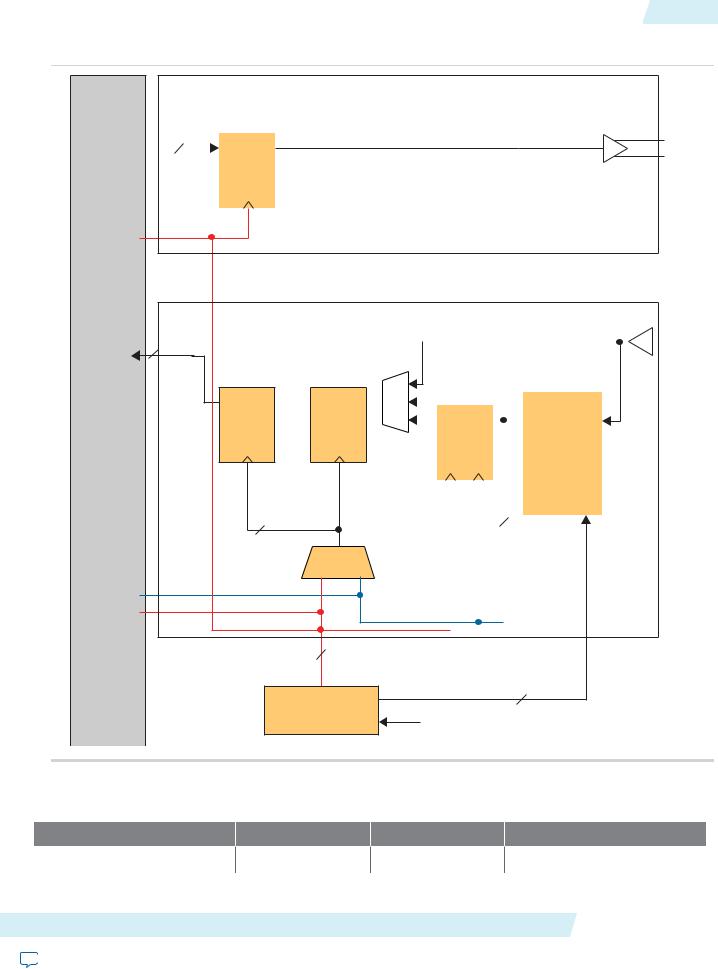
A single Altera LVDS SERDES channel contains a SERDES, a bitslip block, DPA circuitry for all modes, a high-speed clock tree (LVDS clock tree) and forwarded clock signal for soft-CDR mode. You can configure the Altera LVDS SERDES channel as a receiver or a transmitter for a single differential I/O. Therefore, an n-channel LVDS interface contains n-serdes_dpa blocks. The I/O PLLs drive the LVDS clock tree, providing clocking signals to the Altera LVDS SERDES channel in the I/O bank.
Altera Corporation |
Altera LVDS SERDES IP Core User Guide |
Send Feedback
ug_altera_lvds 2014.08.18
Figure 1: Altera LVDS SERDES Channel Diagram
FPGA
Fabric
|
|
|
Serializer |
|
tx_in |
10 |
|
|
|
DIN DOUT |
||||
|
|
|||
|
|
|
|
tx_coreclock
3 lvds_loaden  lvds_fclk tx_coreclock
10
rx_out
Deserializer Bitslip
DOUT DIN  DOUT DIN
fclk
2
loaden
fclk Clock Multiplexer
rx_divfwdclk rx_coreclock
3 lvds_loaden lvds_fclk rx_coreclock
IOPLL
(Local Clock Generator)
Functional Description |
3 |
tx_out
+
-
LVDS Transmitter
LVDS Receiver |
|
|
|
+ |
|
rx_in |
|
|
|||
|
- |
|
|
|
|
|
|
|
|
|
|
|
DPA Circuitry |
|
|
|
DPA FIFO |
|
|
|
|
|
|||
|
|
|
|
|
|
|
|
|
|
|
|
|
DOUT |
DIN |
|
|
|
Retimed |
DIN |
||
|
|
|
|
|
||||||
|
|
|
|
|
|
|
|
|
Data |
|
|
|
|
|
|
|
3 |
|
|
DPA Clock |
|
|
fclklvds |
|
fclkdpa |
|
|
|
|
|||
|
|
|
|
|
|
|||||
|
|
|
|
|
|
|
||||
|
|
|
|
dpa_fclk |
|
|||||
|
|
|
|
|
|
|||||
|
|
|
|
|
|
|
|
dpa_loaden |
|
|
|
|
|
|
|
|
|
|
rx_divfwdclk |
|
|
|
|
|
|
|
|
|
|
|
|
|
|
|
|
|
|
|
|
|
|
|
|
8 Serial LVDS
Clock Phases
rx_inclock/tx_inclock |
|
LVDS Clock Domain |
|
||
|
DPA Clock Domain |
|
|
|
Each Altera LVDS SERDES channel can be broken down into the following paths, with seven functional units:
Path |
Block |
Modes |
Clock Domain |
TX Data Path |
Serializer |
TX mode |
LVDS |
Altera LVDS SERDES IP Core User Guide |
|
|
Altera Corporation |
Send Feedback

4 |
Serializer |
|
|
ug_altera_lvds |
|
|
2014.08.18 |
||
|
|
|
|
|
|
Path |
Block |
Modes |
Clock Domain |
|
|
DPA Circuitry |
DPA FIFO and Soft- |
DPA |
|
|
|
CDR modes |
|
|
RX Data Path |
DPA FIFO |
DPA-FIFO mode |
LVDS-DPA domain crossing |
|
|
Non-DPA and DPA- |
LVDS |
|
|
|
Bitslip and |
||
|
|
FIFO modes |
|
|
|
|
Deserializer |
Soft CDR modes |
DPA clock domain |
|
|
|
||
|
|
Local Clock |
Soft-CDR mode |
Generates PCLK and |
|
Clock Generation and |
Generator |
|
LOADEN in these modes |
|
Multiplexers |
SERDES Clock |
All modes |
Selects LVDS clock sources for |
|
|
Multiplexers |
|
all modes |
Serializer
The serializer consists of two sets of registers. The first set of registers captures the parallel data from the core using the LVDS fast clock. The loaden clock is provided alongside the LVDS fast clock, to enable these capture registers once per coreclock period. After the data is captured, the data is then loaded into a shift register, which shifts the LSB towards the MSB, one bit per fast clock cycle. The MSB of the shift register feeds the LVDS output buffer; hence, higher order bits precede lower order bits in the output bitstream.
The following figure shows the serializer waveform.
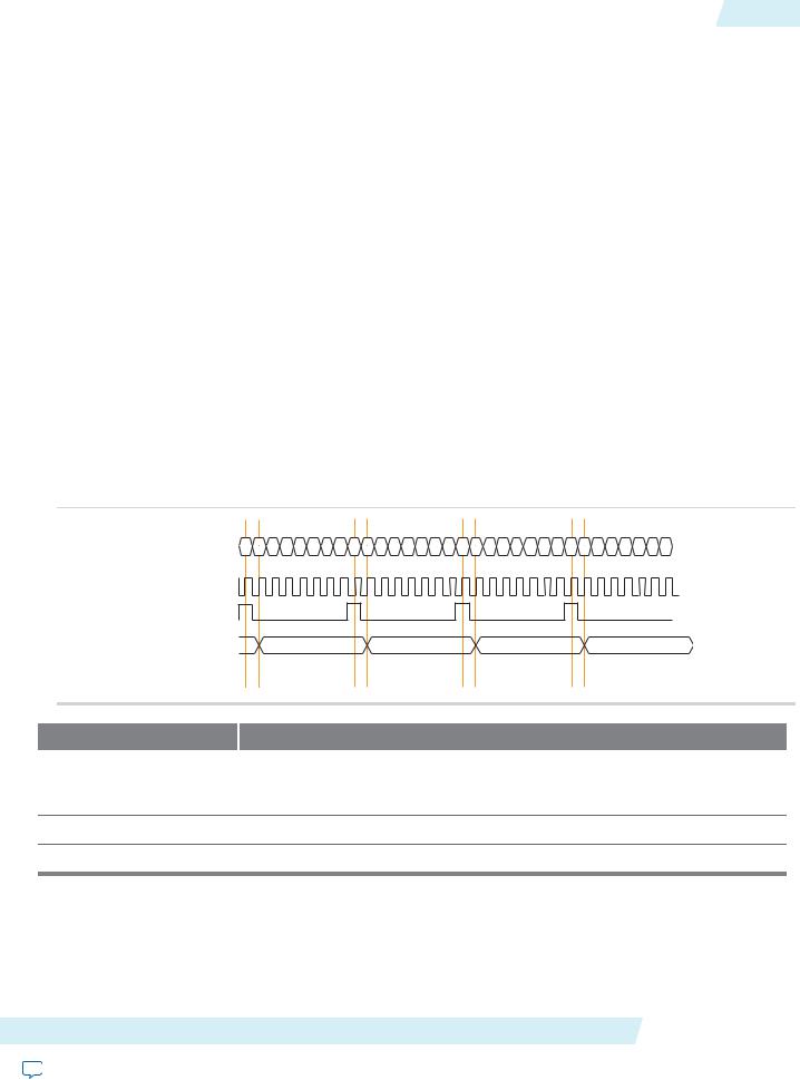
Figure 2: LVDS x8 Serializer Waveform
TXDAT[7:0] |
76543210 |
abcdefgh |
ABCDEFGH |
XXXXXXXX |
FCLK |
|
|
|
|
LOADEN |
|
|
|
|
LVDSOUT |
X X X X X X X X X X 7 6 5 4 3 2 |
1 0 a b c d e f g h A B C D E F |
||
This waveform is specific to serialization factor = 8.
Signal |
Description |
txdat[7:0] |
Data to be serialized (supported serialization factors are 3 -10). |
fclk |
Clock used for transmitter. |
loaden |
Enable signal for serialization. |
lvdsout |
LVDS data stream, output from the Altera LVDS SERDES channel. |
Altera Corporation |
Altera LVDS SERDES IP Core User Guide |
Send Feedback
ug_altera_lvds |
DPA FIFO |
5 |
|
2014.08.18 |
|||
|
|
DPA FIFO
In DPA-FIFO mode, the DPA FIFO synchronizes the retimed data to the high-speed LVDS clock domain. Because the DPA clock may shift phase during the initial lock period, the FIFO must be held in reset state until the DPA locks; otherwise, there may be a data run-through condition due to the FIFO write pointer creeping up to the read pointer.
Bitslip
Use bitslip circuitry to insert latencies in increments of one fclk cycle for data word alignment. The data slips one bit for every pulse of the rx_bitslip_ctrl signal. You must wait at least five core clock cycles before checking if the data is aligned because it will take at least two core clock cycles to purge the undefined data.
When enough bitslip signals are sent to rollover the bitslip counter, the rx_bitslip_max status signal is asserted after five core clock cycles to indicate that it has reached its maximum counter value of the bitslip counter rollover point.
Deserializer
The deserializer consists of shift registers. The deserialization factor determines the depth of the shift registers. The loaden signal is a pulse with a frequency of the fclk divided by the deserialization factor. The deserializer converts a 1-bit serial data stream into a parallel data stream based on the deserialization factor.
Figure 3: LVDS x8 Deserializer Waveform
RX_IN 7 6 5 4 3 2 1 0 a b c d e f g h A B C D E F G H X X X X X X X X
FCLK
LOADEN
RX_OUT[7:0] |
XXXXXXXX |
76543210 |
abcdefgh |
ABCDEFGH |
Signal |
Description |
rx_in |
LVDS data stream, input to the Altera LVDS SERDES channel. |
fclk |
Clock used for receiver. |
loaden
rx_out[7:0]
 Enable signal for deserialization. Deserialized data.
Initialization and Reset
This section describes the initialization and reset aspects, using control characters. This section also provides a recommended initialization and reset flow for the Altera LVDS SERDES IP core.
Altera LVDS SERDES IP Core User Guide |
Altera Corporation |
Send Feedback

6 |
Initializing the Altera LVDS SERDES IP Core |
ug_altera_lvds |
|
2014.08.18 |
|||
|
|
Initializing the Altera LVDS SERDES IP Core
With the Altera LVDS SERDES IP core, the PLL must be locked to the reference clock prior to using the SERDES blocks for data transfer. The PLL starts to lock to the reference clock during device initialization. The PLL is operational when the PLL achieves lock during user mode. If the clock reference is not stable during device initialization, the PLL output clock phase shifts becomes corrupted.
When the PLL output clock phase shifts are not set correctly, the data transfer between the high-speed LVDS domain and the low-speed parallel domain might not be successful, which leads to data corruption. Assert the pll_areset port for at least 10 ns, and then deassert the pll_areset port and wait until the PLL lock becomes stable. After the PLL lock port asserts and is stable, the SERDES blocks are ready for operation.
When using DPA, further steps are required for initialization and reset recovery. The DPA circuit samples the incoming data and finds the optimal phase tap from the PLL to capture data on a receiver channel-by- channel basis. If the PLL has not locked to a stable clock source, the DPA circuit might lock prematurely to a non-ideal phase tap. Use the rx_dpa_reset port to keep the DPA in reset until the PLL lock signal is asserted and stable.
The rx_dpa_locked signal asserts when the DPA has found the optimal phase tap.
Note: Altera recommends asserting the rx_fifo_reset port after the rx_dpa_locked signal asserts, and then deassert the rx_fifo_reset port to begin receiving data.
Each time the DPA shifts the phase taps during normal operation to track variations between the relationship of the reference clock source and the data, the timing margin for the data transfer between clock domains is reduced.
The Altera LVDS SERDES IP core asserts the rx_dpa_locked port upon initial DPA lock. When you enable the Enable DPA loss of lock on one change option, the rx_dpa_locked port deasserts after one change in phase. If this option is disabled, the rx_dpa_locked signal will deassert after two phase changes in the same direction.
Note: Altera recommends using the data checkers to ensure data accuracy.
Resetting the DPA
When the data becomes corrupted, you must reset the DPA circuitry using the rx_dpa_reset port and rx_fifo_reset port.
Assert the rx_dpa_reset port to reset the entire DPA block. This requires the DPA to be trained before it is ready for data capture.
Note: Altera recommends toggling the rx_fifo_reset port after rx_dpa_locked is asserted. This ensures the synchronization FIFO is set with the optimal timing to transfer data between the DPA and highspeed LVDS clock domains.
Assert the rx_fifo_reset port to reset only the synchronization FIFO. This allows you to continue system operation without having to re-train the DPA. Using this port can fix data corruption because it resets the FIFO; however, it does not reset the DPA circuit.
When the DPA is locked, the Altera LVDS SERDES block is ready to capture data. The DPA finds the optimal sample location to capture each bit. The next step is to set up the word boundary using custom logic to control the rx_bitslip_ctrl port on a channel-by-channel basis.
Altera Corporation |
Altera LVDS SERDES IP Core User Guide |
Send Feedback

ug_altera_lvds |
Aligning the Word Boundaries |
7 |
|
2014.08.18 |
|||
|
|
The bitslip circuit can be reset using the rx_bitslip_reset port. This circuit can be reset anytime and is not dependent on the PLL or DPA circuit operation.
Aligning the Word Boundaries
To align the word boundaries, it is useful to have control characters in the data stream so that your logic can have a known pattern to search for. You can compare the data received for each channel, compare to the control character you are looking for, then pulse the rx_bitslip_ctrl port as required until you successfully receive the control character.
Note: Altera recommends setting the bitslip rollover count to the deserialization factor or higher, which allows enough depth in the bitslip circuit to roll through an entire word if required.
If you do not have control characters in the received data, you need a deterministic relationship between the reference clock and data to predict the word boundary using timing simulation or laboratory measurements. This applies only for non-DPA mode. The only way to ensure a deterministic relationship on the default word position in the SERDES when the device powers up, or anytime the PLL is reset, is to have a reference clock equal to the data rate divided by the deserialization factor. For example, if the data rate is 800 Mbps, and the deserialization factor is 8, the PLL requires a 100-MHz reference clock. This is important because the PLL locks to the rising edge of the reference clock. If you have one rising edge on the reference clock per serial word received, the deserializer always starts at the same position. Using timing simulation, or lab measurements, monitor the parallel words received and determine how many pulses are required on the rx_bitslip_ctrl port to set your word boundaries. You can create a simple state machine to apply the required number of pulses when you enter user mode, or anytime you reset the PLL.
Note: When using DPA or soft-CDR modes, the word boundary is not deterministic. The initial training of the DPA allows it to move forward or backward in phase relative to the incoming serial data. Thus, there can be a ± 1-bit of variance in the serial bit where the DPA initially locks. If there are no training patterns or control characters available in the serial bit stream to use for word alignment, Altera recommends using non-DPA mode.
Recommended Initialization and Reset Flow
Altera recommends that you follow these steps to initialize and reset the Altera LVDS SERDES IP core:
1.During entry into user mode, or anytime in user mode operation when the interface requires a reset, assert the pll_areset and rx_dpa_reset ports.
2.Deassert the pll_areset port and monitor the pll_locked port. For non-DPA mode, skip to step 7.
3.Deassert the rx_dpa_reset port after the pll_locked port becomes asserted and stable.
4.Apply the DPA training pattern and allow the DPA circuit to lock. (If a training pattern is not available, any data with transitions is required to allow the DPA to lock.) Refer to the respective device data sheet for DPA lock time specifications.
5.Wait for the rx_dpa_locked port to assert.
6.Assert rx_fifo_reset for at least one parallel clock cycle, and then de-assert rx_fifo_reset.
7.Assert the rx_bitslip_reset port for at least one parallel clock cycle, and then deassert the
rx_bitslip_reset port.
8.Begin word alignment by applying pulses as required to the rx_bitslip_ctrl port.
9.When the word boundaries are established on each channel, the interface is ready for operation.
Altera LVDS SERDES IP Core User Guide |
Altera Corporation |
Send Feedback
8 |
Signals |
ug_altera_lvds |
|
2014.08.18 |
|||
|
|
Signals
The following tables list the input and output signals for the Altera LVDS SERDES IP core.
Note: N represents the LVDS interface width and the number of serial channels while J represents the SERDES factor of the interface.
Table 2: Common TX and RX Signals
Signal Name |
Width |
Direction |
Type |
Description |
inclock |
1 |
Input |
Clock |
PLL reference clock. |
pll_areset |
1 |
Input |
Reset |
Active-high asynchronous reset to all blocks |
|
|
|
|
in Altera LVDS SERDES and PLL. |
pll_locked
1 |
Output Control Asserted when internal PLL is locked. |
Table 3: RX Signals
Signal Name |
Width |
Direction |
Type |
Description |
rx_in |
N |
Input |
Data |
LVDS serial input data. |
rx_bitslip_reset |
N |
Input |
Reset |
Asynchronous, active-high reset to the clock- |
|
|
|
|
data alignment circuitry (bitslip). |
rx_bitslip_ctrl |
N |
Input |
Control |
Positive-edge triggered increment for bitslip |
|
|
|
|
circuitry. Each assertion adds one bit of |
|
|
|
|
latency to the received bitstream. |
rx_dpa_hold |
N |
Input |
Control |
Asynchronous, active-high signal prevents |
|
|
|
|
the DPA circuitry from switching to a new |
|
|
|
|
clock phase on the target channel. When held |
|
|
|
|
high, the selected channel(s) hold their |
|
|
|
|
current phase setting. When held low, the |
|
|
|
|
DPA block on selected channel(s) monitors |
|
|
|
|
the phase of the incoming data stream |
|
|
|
|
continuously and selects a new clock phase |
|
|
|
|
when needed. Applicable in DPA-FIFO and |
|
|
|
|
soft-CDR modes only. |
rx_dpa_reset
rx_fifo_reset
N |
Input |
Reset |
Asynchronous, active-high reset to DPA |
|
|
|
blocks. Minimum pulse width is one parallel |
|
|
|
clock period. Applicable in DPA-FIFO and |
|
|
|
soft-CDR modes only. |
N |
Input |
Reset |
Asynchronous, active-high reset to FIFO |
|
|
|
block. Minimum pulse width is one parallel |
|
|
|
clock period. Applicable in DPA-FIFO mode |
|
|
|
only. |
Altera Corporation |
Altera LVDS SERDES IP Core User Guide |
Send Feedback
ug_altera_lvds |
|
|
|
Signals |
9 |
2014.08.18 |
|
|
|
||
|
|
|
|
|
|
Signal Name |
Width |
Direction |
Type |
Description |
|
rx_out |
N*J |
Output |
Data |
Receiver parallel data output. Synchronous |
|
|
|
|
|
to rx_coreclock in (DPA-FIFO and non- |
|
|
|
|
|
DPA modes). In soft-CDR mode, each |
|
|
|
|
|
channel has parallel data synchronous to its |
|
|
|
|
|
rx_divfwdclk. |
|
rx_bitslip_max |
N |
Output |
Control |
Bitslip rollover signal. High when the next |
|
|
|
|
|
assertion of rx_bitslip_ctrl resets the serial |
|
|
|
|
|
bit latency to 0. |
|
rx_coreclock |
1 |
Output |
Clock |
Core clock for RX interfaces provided by the |
|
|
|
|
|
PLL. Not available when using an external |
|
|
|
|
|
PLL. |
|
rx_divfwdclk |
N |
Output |
Clock |
The per channel, divided clock with the ideal |
|
|
|
|
|
DPA phase. The recovered slow clock for a |
|
|
|
|
|
given channel. Applicable in soft-CDR mode |
|
|
|
|
|
only. Because each channel may have a |
|
|
|
|
|
different ideal sampling phase, the rx_ |
|
|
|
|
|
divfwdclks may not be edge-aligned with |
|
|
|
|
|
each other. Each rx_divfwdclk must drive |
|
|
|
|
|
the core logic with data from the same |
|
|
|
|
|
channel. |
|
rx_dpa_locked |
N |
Output |
Control |
Asserted when the DPA block selects the ideal |
|
|
|
|
|
phase. The Altera LVDS SERDES IP core |
|
|
|
|
|
drives the rx_dpa_locked port. The DPA |
|
|
|
|
|
logic asserts the rx_dpa_locked signal when |
|
|
|
|
|
the signal settles on an ideal phase for that |
|
|
|
|
|
given channel. The rx_dpa_locked port will |
|
|
|
|
|
de-assert if the DPA moves two phases in the |
|
|
|
|
|
same direction or if the DPA moves one |
|
|
|
|
|
phase. The rx_dpa_locked signal will still |
|
|
|
|
|
toggle when the rx_dpa_hold signal is |
|
|
|
|
|
asserted, and should be ignored by user logic |
|
|
|
|
|
when the rx_dpa_hold signal is asserted. |
|
|
|
|
|
Applicable in DPA-FIFO and soft-CDR |
|
|
|
|
|
modes only. |
|
Table 4: TX Signals |
|
|
|
|
|
Signal Name |
Width |
Direction |
Type |
Description |
|
tx_in
tx_out
tx_outclock
N*J |
Input |
Data |
Parallel data from the core. |
N |
Output |
Data |
LVDS serial output data. |
1 |
Output |
Clock |
External reference clock (sent off chip via the |
|
|
|
TX data path). Source-synchronous with tx_ |
|
|
|
out. |
Altera LVDS SERDES IP Core User Guide |
Altera Corporation |
Send Feedback
Loading...