

Page 1

Product Transition Guide – J7 to J1000
(Header Title) Application Note
Product Transition Guide
J7 to J1000
Doc#: PL.J1000.01 Copyright Yaskawa Electric America, Inc.©2008 www.yaskawa.com August 1, 2008 1 of 19
Page 2

Product Transition Guide – J7 to J1000
(Header Title) Application Note
Subject: Transition Guide Product: J1000 Document: PL.J1000.01
Title: Product Transition Guide – J7 to J1000
Table of Contents
1.0 APPLICABLE DRIVES ……………………………………………………………….. 3
2.0 DRIVE REPLACEMENT CHECKLIST ……………………………………………… 4
3.0 RATINGS SUMMARY ………………………………………………………………… 5
4.0 TERMINALS …………………………………………………………………………… 6
4.1 Main Circuit Terminals ……………………………………………………….. 6
4.2 Control Terminals, Signal Levels ………………………………………….. 6
4.3 DIP Switches …………………………………………………………………... 7
4.4 Main Terminal Size / Electric Wire Differences …………………………. 7
4.5 Control Terminal and Wire Sizes …………………………………………... 9
5.0 DIMENSIONS…………………………………………………………………...……... 10
6.0 OPTION REPLACEMENTS …………………………………………………………. 11
7.0 PARAMETER SETTINGS ……………………………………………………………. 12
7.1 Parameter Correspondence for Drive Replacement ………………...…. 12
7.2 Parameter Differences ……………………………………………………….. 18
7.3 Special Software Replacement ………………...…………………………... 18
8.0 REVISION HISTORY …………………………………………………………………. 19
9.0 REFERENCES ………………………………………………………………………… 19
Doc#: PL.J1000.01 Copyright Yaskawa Electric America, Inc.©2008 www.yaskawa.com August 1, 2008 2 of 19
Page 3

Product Transition Guide – J7 to J1000
(Header Title) Application Note
Subject: Transition Guide Product: J1000 Document: PL.J1000.01
Title: Product Transition Guide – J7 to J1000
1.0 Applicable Drives
This document describes the substitution of the following drives:
Original Drive: CIMR-J7xMxxxx, CIMR-J7xUxxx, or JDxxxx
Spec: xxxx0 (IP20)
Software Version: Standard: 001x, 002x
Replacement: CIMR-JUxAxxxxBxx
Spec: CIMR-JUxAxxxxBxx (A-Standard model)
Software Version: PRG: 10xx
This replacement J1000 drive must be selected using the J1000 Heavy Duty rating.
The description is not valid for drives with other specifications or firmware installed.
Doc#: PL.J1000.01 Copyright Yaskawa Electric America, Inc.©2008 www.yaskawa.com August 1, 2008 3 of 19
Page 4

Product Transition Guide – J7 to J1000
(Header Title) Application Note
Subject: Transition Guide Product: J1000 Document: PL.J1000.01
Title: Product Transition Guide – J7 to J1000
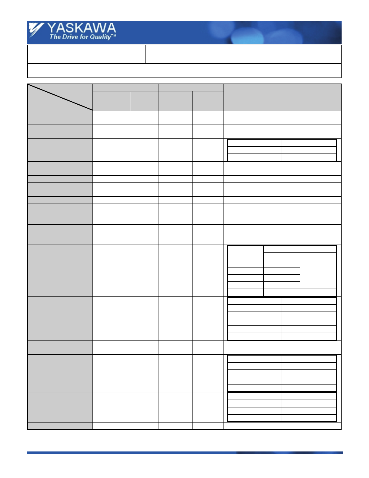
2.0 Drive Replacement Checklist
Hardware
Software
Options,
Others
Item Checkpoints Checked?
Digital Operator Panel
Does the digital operator panel need to be mounted in the same location as
before?
- If necessary, attempt to mount the operator panel at the same location as
before.
Basic
Main and
Control
Te r mi n al s
Software
Version
Parameter
Communi-
cation
Option
Reactors,
Chokes
Filters
Cables
Was a remote operator connected to the old unit?
- If so, do not attempt to connect the old remote operator panel to the J1000.
Refer to part 6 of this document for option replacements.
Special Specifications
Check the installed drive’s specifications to make sure that it is compliant with the
standard specifications (no special firmware, etc.).
Wire Length
In the J7 drive, the main terminals are located at the top of the drive. The J1000
drive has all main terminals located at the bottom of the drive. Check to assure
that all cables are long enough to be connected without tension to the new drive.
Main Circuit Wires and Terminal Specifications
Compare the occupied terminals of the old drive to the new drive’s terminals
(shape, size, etc.). Check that all wires fit in the new drive’s terminals, refer to part
4 of this document.
Check Software Version or for Special Software
Check the software number in the old drive to be sure that it can be replaced by
the J1000 drive. Refer to part 7.3 of this document.
- Ask your Yaskawa representative for help in identifying the software installed
on the drive that must be replaced and for additional replacement information.
Check the Parameter Settings
Check the parameter settings of the J7 drive and perform a parameter transition to
the new parameters following part 7 of this document. Contact your Yaskawa
representative if there is special software installed or if a parameter is not
mentioned in this document.
Is an Option Card Installed?
Check if any communication card options are installed.
- J7 options are NOT compatible with the J1000 drive and must be replaced.
- Communication cable connectors from J7 options are compatible to the J1000
options without rewiring.
Is an AC Reactor or DC Link Choke Installed?
AC Reactors or DC Link Chokes installed on a J7 drive are compatible with the
J1000 drive.
Is an EMC Filter Installed?
Some EMC Filters installed on a J7 drive are compatible with the J1000 drive. For
details on filter replacements contact your Yaskawa representative.
Extension Cables
The extension cables for remote operation used on a J7 drive are compatible with
the J1000 drive. However, the remote operator and the remote operator interface
are not compatible with the J1000 drive and must be replaced.
• For questions on installation, parameter settings or detailed parameter/ function descriptions see the
instruction manual. Other technical questions should be referred to your Yaskawa representative.
Doc#: PL.J1000.01 Copyright Yaskawa Electric America, Inc.©2008 www.yaskawa.com August 1, 2008 4 of 19
Page 5
Product Transition Guide – J7 to J1000
(Header Title) Application Note
Subject: Transition Guide Product: J1000 Document: PL.J1000.01
Title: Product Transition Guide – J7 to J1000
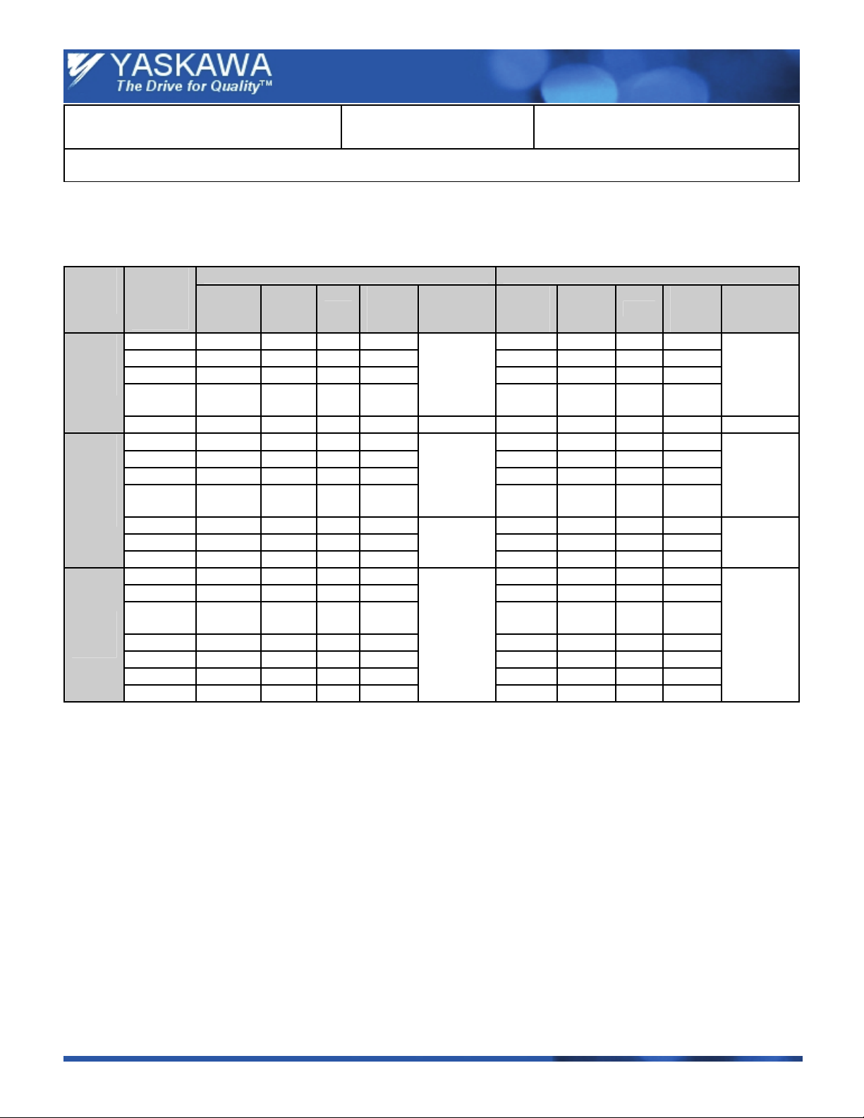
3.0 Ratings Summary
<1>, <3>
J7 J1000
HP
& 1
& 1
Output
Current
(A)
5.0
5.0
Carrier
Frequency
(kHz)
10
10
7.5
7.5
Model
No.
JUx
BA0006 1.9 3/4 & 1 5.0
2A0006 1.9 3/4 & 1 5.0
2A0020 6.7 5 17.5
4A0011 7.0 5 9.2
Output
Power
(kVA)
HP
Output
Current
(A)
Voltage
Class
Single
Phase
200 V
ThreePhase
200 V
ThreePhase
400 V
Maximum
Motor
Power
(kW)
0.1 B0P1 0.3 1/8 0.8 BA0001 0.3 1/8 0.8
0.2 B0P2 0.6 1/4 1.6 BA0002 0.6 1/4 1.6
0.4 B0P4 1.1 1/2 3.0 BA0003 1.1 1/2 3.0
0.75 B0P7 1.9 3/4
1.5 B1P5 3.0 2 8.0 7.5 BA0010 3.0 2 8.0 8
0.1 20P1 0.3 1/8 0.8 2A0001 0.3 1/8 0.8
0.2 20P2 0.6 1/4 1.6 2A0002 0.6 1/4 1.6
0.4 20P4 1.1 1/2 3.0 2A0004 1.1 1/2 3.0
0.75 20P7 1.9 3/4
1.5 21P5 3.0 2 8.0 2A0010 3.0 2 8.0
2.2 22P2 4.2 3 11.0 2A0012 4.2 3 11.0
3.7 23P7 6.7 5 17.5
0.2 40P2 0.9 1/2 1.2 4A0001 0.9 1/2 1.2
0.4 40P4 1.4 3/4 1.8 4A0002 1.4 3/4 1.8
0.75 40P7 2.6 1 & 2 3.4 4A0004 2.6 1 & 2 3.4
1.5 41P5 3.7 3 4.8 4A0005 3.7 3 4.8
2.2 42P2 4.2 3 5.5 4A0007 4.2 3 5.5
2.2 42P2 4,2 3 5,5 4A0009 5.5 4 7.2
3.7 43P7 6.6 5 8.6
Model
No.
J7xMx
Output
Power
(kVA)
Carrier
Frequency
(kHz)
10
10
8
8
Doc#: PL.J1000.01 Copyright Yaskawa Electric America, Inc.©2008 www.yaskawa.com August 1, 2008 5 of 19
Page 6
Product Transition Guide – J7 to J1000
(Header Title) Application Note
Subject: Transition Guide Product: J1000 Document: PL.J1000.01
Title: Product Transition Guide – J7 to J1000
4.0 Terminals
4.1 Main Circuit Terminals
Note: The J7 and J1000 drives may have different terminal sizes (depending on capacity); therefore, the terminals must be
carefully checked before replacement. The main terminal functionality has not been changed.
J7 Main
Terminals
R / L 1 R / L 1
S / L2 S / L2
T / L 3 T / L 3
U / T1 U / T1
V / T2 V / T2
W / T3 W / T3
- B1 Braking resistor or external braking chopper connection.
- B2 Braking resistor connection.
+1 +1
+2 +2
+1 +1
— —
J1000 Main
Terminals
Power supply connection.
Note:
In the J7 drive the power supply terminals are located at the top of the drive. In the J1000
the power supply terminals are located at the bottom of the drive. Cables must fit without
tension (replace or extend if needed).
Drive Output
DC Link Choke connection, DC Power Supply input.
DC Power Supply input, external braking transistor module connection.
Grounding Terminal: For 200 V class: 100 Ω or less
For 400 V class: 10 Ω or less
Note
4.2 Control Terminals, Signal Levels
Terminal Signal Level
J7 J1000
S1
S2
S3
S4
S5 Multi-function input 5 (Multi speed 1)
SC Multi-function input common. — —
FS +V Analog input power supply. +12 Vdc, max. 20 mA +10.5 Vdc, max. 20 mA
FR A1
FC AC Analog input common. 0 V
MA
MB
MC Change over contact output common.
AM Analog output.
AC
Multi-function input 1
(1: Run forward, 0: Stop)
Multi-function input 2
(1: Run reverse, 0: Stop)
Multi-function input 3
(J7: Fault Reset / J1000: Ext. Fault)
Multi-function input 4
(J7: Ext. Fault / J1000: Fault Reset)
Analog input 1
(Frequency Reference)
Change over contact output (NO).
(Fault)
Change over contact output (NC).
(Fault)
Analog output GND
Function
J7 J1000
Photo coupler isolation
+24 Vdc, 8 mA
0 ~ +10 Vdc (20 kΩ)
0 or 4-20 mA (250 Ω)
Maximum Load
250 Vac , 10 mA ~ 1A
30 Vdc, 10 mA ~ 1 A
0 ~ +10 Vdc,
Maximum 2 mA
Resolution 8 Bit
Photo coupler isolation
+24 Vdc, 8 mA
0 ~ +10 Vdc (20 kΩ)
0 or 4-20 mA (250 Ω)
Maximum Load
250 Vac , 10 mA ~ 1A
30 Vdc, 10 mA ~ 1 A
0 ~ +10 Vdc,
maximum 2 mA
Resolution 8 Bit
Doc#: PL.J1000.01 Copyright Yaskawa Electric America, Inc.©2008 www.yaskawa.com August 1, 2008 6 of 19
Page 7

Product Transition Guide – J7 to J1000
(Header Title) Application Note
Subject: Transition Guide Product: J1000 Document: PL.J1000.01
Title: Product Transition Guide – J7 to J1000
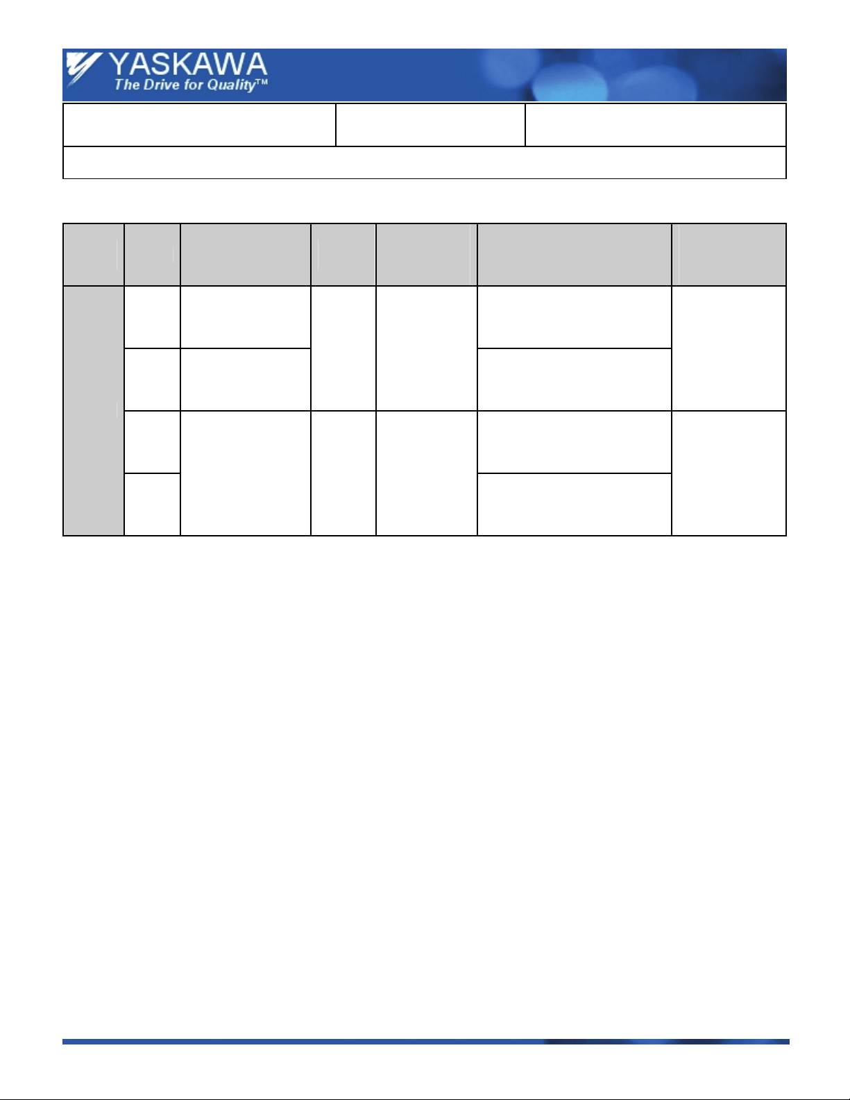
4.3 DIP Switches
Note: When replacing a J7 drive with a J1000 drive, verify that DIP Switches (S1 and S3) are set properly.
Function
NPN / PNP Selection SW7 NPN S3 SINK (NPN)
Analog input 1 level selection SW8 Voltage S1 Voltage
Switch Default Switch Default
4.4 Main Terminal Size / Electric Wire Differences
Note: The J7 drive has main terminals at the top and bottom, while the J1000 drive has all main terminals at the bottom. Ensure
that all wires fit without tension.
= Ground Terminal
Voltage
Class
Three –
Phase
200 V
Drive
J7
J1000
J7
J1000
J7
J1000
J7
J1000
CIMR-
JU
20P1
20P2
20P4
20P7
2A0001
2A0002
2A0004
2A0006
21P5
2A0010
22P2
2A0012
23P7
2A0020
Terminal Symbol
R / L1, S / L2, T / L3,
—, +1, +2,
U / T1, V / T2, W / T3
R / L1, S / L 2, T / L3,
U / T1, V / T2, W / T3,
—, +1, +2, B1, B2,
(2 terminals)
R / L1, S / L 2, T / L3,
U / T1, V / T2, W / T3,
—, +1, +2
R / L1, S / L 2, T / L3,
U / T1, V / T2, W / T3,
—, +1, +2, B1, B2
(2 terminals)
R / L1, S / L 2, T / L3,
U / T1, V / T2, W / T3,
—, +1, +2,
R / L1, S / L 2, T / L3,
U / T1, V / T2, W / T3,
—, +1, +2, B1, B2,
(2 terminals)
R / L1, S / L 2, T / L3,
U / T1, V / T2, W / T3,
—, +1, +2,
R / L1, S / L 2, T / l3, U
/ T1, V / T2, W / T3, —,
+1, +2, B1, B2, (2
terminals)
J7 J1000
Tightening
Screw
Size
M3.5
M3.5
M4
M3.5
M4 1.2 ~ 1.5
M4
Torque
N.m
(lb - in.)
0.8 ~ 1.0
(7.1 to 8.9)
(11.0)
0.8 ~ 1.0
(7.1 to 8.9)
0.8 ~ 1.0
(7.1 to 8.9)
1.2 ~ 1.5
(10.6 to 13.3)
0.8 ~ 1.0
(7.1 to 8.9)
(10.6 to 13.3)
1.2 ~ 1.5
(10.6 to 13.3)
1.24
Wire Size
2
mm
(AWG)
0.75 ~ 2.0
(18 to 14)
2.0 ~ 5.5
(14 to 10)
2.0 ~ 5.5
(14 to 10)
2.0 ~ 5.5
(14 to 10)
2.0 ~ 5.5
(14 to 10)
Recommended
Wire Size
2
mm
(AWG)
2
(14)
2
(14)
2
(14)
3.5
(12)
3.5
(12)
5.5
(10)
Doc#: PL.J1000.01 Copyright Yaskawa Electric America, Inc.©2008 www.yaskawa.com August 1, 2008 7 of 19
Page 8

Product Transition Guide – J7 to J1000
(Header Title) Application Note
Subject: Transition Guide Product: J1000 Document: PL.J1000.01
Title: Product Transition Guide – J7 to J1000
Voltage
Class
Single –
Phase
200 V
Three –
Phase
400 V
Drive
J7
J1000
J7 B0P7
J1000 BA0006
J7 B1P5
J1000 BA0010
J7
J1000
J7 42P2
J1000 4A0007
J7
J1000
CIMR-
JU
B0P1
B0P2
B0P4
BA0001
BA0002
BA0003
40P2
40P4
40P7
41P5
4A0001
4A0002
4A0004
4A0005
43P0
43P7
4A0009
4A0011
R / L1, S / L 2,
—, +1, +2,
U / T1, V / T2, W / T3 1.24 (11.0)
R / L1, S / L 2,
U / T1, V / T2, W /
T3,—, +1, +2, B1, B2,
R / L1, S / L 2,
U / T1, V / T2, W / T3,
—, +1, +2
R / L1, S / L 2,
U / T1, V / T2, W / T3,
—, +1, +2, B1, B2,
R / L1, S / L 2,
U / T1, V / T2, W / T3,
—, +1, +2
R / L1, S / L 2,
U / T1, V / T2, W / T3,
—, +1, +2, B1, B2,
R / L1, S / L 2, T / L3,
U / T1, V / T2, W / T3,
—, +1, +2,
R / L1, S / L 2, T / L3,
U / T1, V / T2, W / T3,
—, +1, +2, B1, B2,
R / L1, S / L 2, T / L3,
U / T1, V / T2, W / T3,
—, +1, +2,
R / L1, S / L 2, T / L3,
U / T1, V / T2, W / T3,
—, +1, +2, B1, B2,
R / L1, S / L 2, T / L3,
U / T1, V / T2, W / T3,
—, +1, +2
R / L1, S / L 2, T / L3,
U / T1, V / T2, W / T3,
—, +1, +2, B1, B2
Terminal Symbol
(2 terminals)
(2 terminals)
(2 terminals)
(2 terminals)
(2 terminals)
(2 terminals)
Screw
Size
M3.5
M3.5
M4
M3.5
M4
M3.5
M4
M4
M4
M4
Tightening
Torque
N.m
(lb - in.)
0.8 ~ 1.0
(7.1 to 8.9)
0.8 ~ 1.0
(7.1 to 8.9)
0.8 ~ 1.0
(7.1 to 8.9)
1.2 ~ 1.5
(10.6 to 13.3)
0.8 ~ 1.0
(7.1 to 8.9)
1.2 ~ 1.5
(10.6 to 13.3)
0.8 ~ 1.0
(7.1 to 8.9)
1.2 ~ 1.5
(10.6 to 13.3)
1.2 ~ 1.5
(10.6 to 13.3)
1.2 ~ 1.5
(10.6 to 13.3)
1.2 ~ 1.5
(10.6 to 13.3)
Wire Size
2
mm
(AWG)
0.75 ~ 2.0
(18 to 14)
2.0 ~ 5.5
(14 to 10)
2.0 ~ 5.5
(14 to 10)
2.0 ~ 5.5
(14 to 10)
2.0 ~ 5.5
(14 to 10)
2.0 ~ 5.5
(14 to 10)
2.0 ~ 5.5
(14 to 10)
Recommended
Wire Size
2
mm
(AWG)
2
(14)
3.5
(12)
2
(14)
2
(14)
5.5
(10)
2 (14)
3.5
(12)
5.5 (10)
2
(14)
2
(14)
2
(14)
3.5 (12)
2
(14)
3.5
(12)
Doc#: PL.J1000.01 Copyright Yaskawa Electric America, Inc.©2008 www.yaskawa.com August 1, 2008 8 of 19
Page 9
Product Transition Guide – J7 to J1000
(Header Title) Application Note
Subject: Transition Guide Product: J1000 Document: PL.J1000.01
Title: Product Transition Guide – J7 to J1000
4.5 Control Terminal and Wire Sizes
Voltage
Class
All
Drive Terminal Symbol
J7
J1000
J7
J1000
S1 - S5, SC, FS, FR,
FC, AM, AC
S1 - S5, SC, V+, A1,
AC, AM, AC
MA, MB, MC M3
Screw
Size
M2
Tightening
Torque
N.m
(lb - in.)
0.22 ~ 0.25
(1.9 to 2.2)
0.5 ~ 0.6
(4.4 to 5.3)
Wire Size
2
mm
(AWG)
Flexible: 0.5 ~ 0.75
(20 to 18)
Solid: 0.5 ~ 1.25
(20 to 18)
Flexible: 0.25 ~ 1.0
(24 to 18)
Solid: 0.25 ~ 1.5
(24 to 16)
Flexible: 0.5 ~ 0.75
(20 to 18)
Solid: 0.5 ~ 1.25
(20 to 18)
Flexible: 0.25 ~ 1.0
(24 to 18)
Solid: 0.25 ~ 1.5
(24 to 16)
Recommended
Wire Size
mm2
(AWG)
0.75
(18)
0.75
(18)
Doc#: PL.J1000.01 Copyright Yaskawa Electric America, Inc.©2008 www.yaskawa.com August 1, 2008 9 of 19
Page 10

Product Transition Guide – J7 to J1000
(Header Title) Application Note
Subject: Transition Guide Product: J1000 Document: PL.J1000.01
Title: Product Transition Guide – J7 to J1000
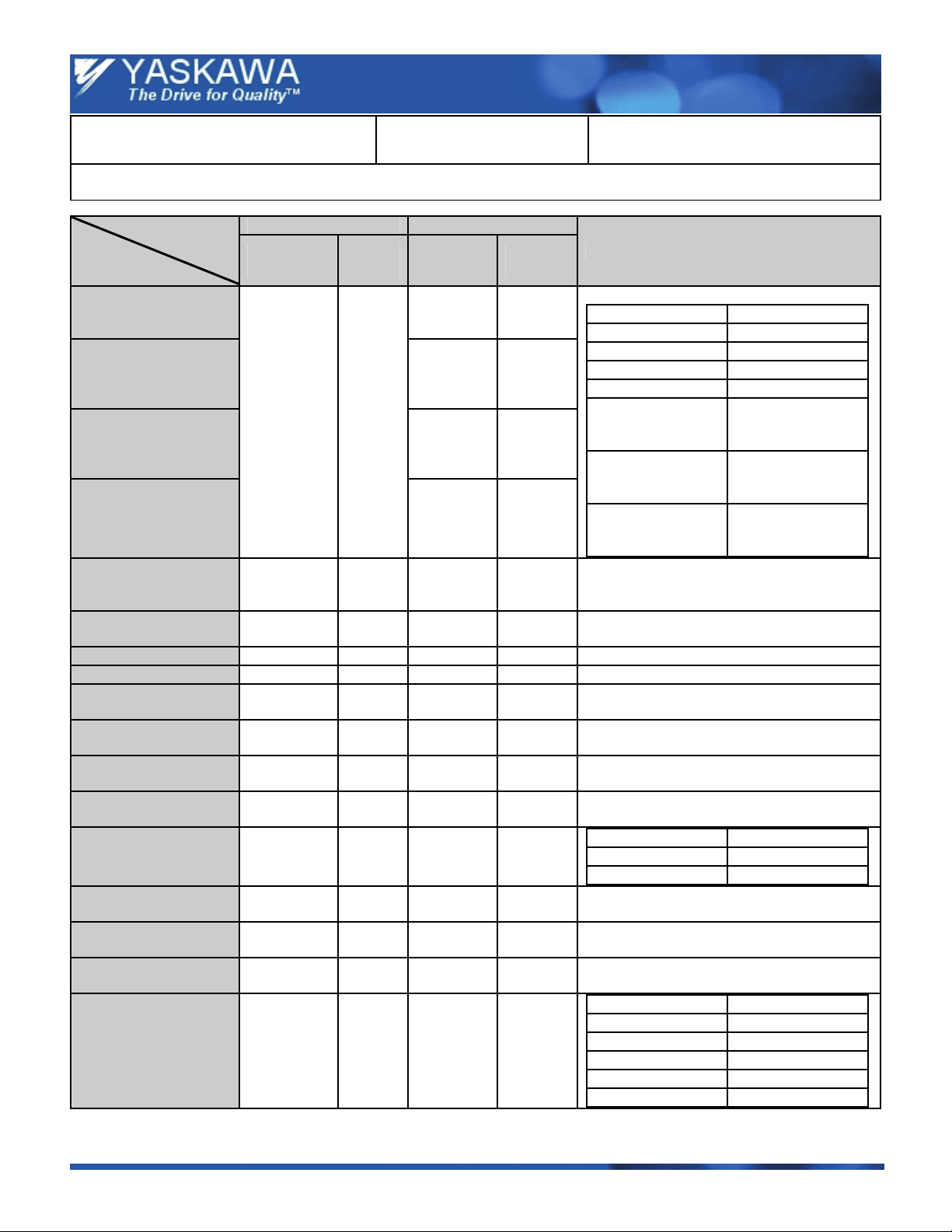
5.0 Dimensions
Note: The tables below show dimension differences between the J7 and the J1000 (in mm and in) and the required parts for the
drive replacement (J7 dimensions are without potentiometer knob).
Voltage
Class
Single
Phase 200 V
Three Phase
200 V
Three Phase
400 V
Voltage
Class
Single
Phase 200 V
Three Phase
200 V
Three Phase
400 V
J7
CIMR-
J7xM
B0P10 BA0001B
B0P20
B0P40
B0P70 129 BA0006B 137.5
B1P50
20P10 2A0001B
20P20
20P40 102 2A0004B 108
20P70
21P50 129 2A0010B 129
21P20
23P70 140
40P20 81 4A0001B 81
40P40 99 4A0002B 99
40P70 129 4A0004B 137.5
41P50 4A0005B
42P20
43P70 140
J7
CIMR-
J7xM
B0P10 BA0001B
B0P20
B0P40
B0P70 5.08 BA0006B 5.41
B1P50
20P10 2A0001B
20P20
20P40 4.02 2A0004B 4.25
20P70
21P50 5.08 2A0010B 5.08
21P20
23P70 5.51
40P20 3.19 4A0001B 3.19
40P40 3.90 4A0002B 3.90
40P70 5.08 4A0004B 5.41
41P50 4A0005B
42P20
43P70 5.51
W
(mm)
68
108
68
108
108
W
(in)
2.68
4.25
2.68
4.25
4.25
J7 J1000
H
(mm)
128
128
128
J7 J1000
H
(in)
5.04
5.04
5.04
D
(mm)
70
112 B10003B
154 BA0010B
70
122 2A0006B
154 2A0012B
161 2A0020B 140
154
161 4A0011B 140
D
(in)
2.76
4.41 B10003B
6.06 BA0010B
2.76
4.80 2A0006B
6.06 2A0012B
6.34 2A0020B 5.51
6.06
6.34 4A0011B 5.51
J1000
CIMR-
JU
BA0002B
2A0002B
4A0007B
J1000
CIMR-
JU
BA0002B
2A0002B
4A0007B
W
(mm)
68
108
68
108
108
W
(in)
2.68
4.25
2.68
4.25
4.25
(mm)
5.04
5.04
5.04
H
128
128
128
H
(in)
D
(mm)
76
118
154
76
128
137.5
143
154
143
D
(in)
2.99
4.65
6.06
2.99
5.04
5.41
5.63
6.06
5.63
Doc#: PL.J1000.01 Copyright Yaskawa Electric America, Inc.©2008 www.yaskawa.com August 1, 2008 10 of 19
Page 11

Product Transition Guide – J7 to J1000
(Header Title) Application Note
Subject: Transition Guide Product: J1000 Document: PL.J1000.01
Title: Product Transition Guide – J7 to J1000
6.0 Option Replacements
The table below indicates potential option replacements.
Note: J7 options are not compatible with the J1000 drive.
Type Description J7 J1000
Interface for Remote Operator SI-232 / J7 SI-232 / J
Serial
Communications
Operator Panel
Potentiometer
Option
DIN Rail Mounting Used to mount the drive on a DIN Rail. EZZ08122x EZZ08122x
AC Reactor 3% or 5% AC Line Reactor 05P00620-xxxx 05P00620-xxxx
DC Link Choke 3% DC Link Choke 05P00620-xxxx 05P00620-xxxx
Copy Unit
Interface for RS-232 PC communication
(MEMOBUS / Modbus)
Interface for RS-422 / 485 communication
(MEMOBUS / Modbus)
Remote operator without potentiometer JVOP-146 JVOP-182
Remote operator with potentiometer JVOP-144 Not Available
Extension Cable 1 meter UWR0051 UWR0051
Extension Cable 3 meter UWR0052 UWR0052
To use a potentiometer on the drive for settings up the
frequency reference.
Copy unit or keypads used to upload / download drive
parameters from one drive to another.
SI-232 / J7C SI-232 / JC
SI-485 / J7 SI-485 / J
Built-in AI-V3 / J
JV0P-140 or
JV0P-142
and
• SI-232 / J7 or / J7C
and
• UWR0051 (1 m )
or
• UWR0052 (3 m)
JV0P-182
(LED operator)
or JV0P-181
(USB Copy Unit)
• SI-232 / J or / J7C
• Same cables as J7
and
and
Doc#: PL.J1000.01 Copyright Yaskawa Electric America, Inc.©2008 www.yaskawa.com August 1, 2008 11 of 19
Page 12

Product Transition Guide – J7 to J1000
(Header Title) Application Note
Subject: Transition Guide Product: J1000 Document: PL.J1000.01
Title: Product Transition Guide – J7 to J1000
7.0 Parameter Settings
7.1 Parameter Correspondence for Drive Replacement
Note:
1. Before setting up other parameters, verify that C6-01 is set to “0” (HD). Refer to the Technical Manual for details on the
Normal and Heavy Duty selection.
2. Voltage values are valid for a 200 V drive. Voltage values double for the 400 V drive.
J7 J1000 Drive
Function
/ Parameter
Parameter Access
Level
Initialization A1-03 0
RUN command in
Programming Mode
Fault History U2
Initialization
RUN Command Source
Selection
Frequency Reference
Source Selection
Stop Method Selection n04 0 b1-03 0
Reverse Run Prohibit
Selection
Digital Operator STOP
Key Function
Frequency Reference in
Local Mode
Parameter
No.
n01 1
n02 1 b1-02 1
n03 2 b1-01 1
n05 0 b1-04 0
n06 0
n07 0 — — (No operator panel potentiometer)
Initial
Value
Parameter
No.
A1-01 2
b1-08 0
o4-11 0
o2-02
Initial
Value
1
n01 Æ 0 A1-01 Æ 0
n01 Æ 1 A1-01 Æ 2
n01 Æ 5 A1-01 Æ 2
n01 Æ 6 o4-11 Æ 1
n01 Æ 10 A1-03 Æ 2220
n01 Æ 11 A1-03 Æ 3330
n02 Æ 0 b1-02 Æ 0
n02 Æ 1 b1-02 Æ 1
n02 Æ 2 b1-02 Æ 2
n03 Æ 0 b1-01 Æ 0 (A1-V3 / J
n03 Æ 1 b1-01 Æ 0
n03 Æ 2 b1-01 Æ 1 & H3-01 Æ 0
n03 Æ 3 b1-01 Æ 1 & H3-01 Æ 2
n03 Æ4 b1-01 Æ 1 & H3-01 Æ 3
n03 Æ 6 b1-01 Æ 2
When using A1 as frequency reference input,
make sure to set DIP switch S1 properly
(voltage or current input).
J7 J1000
n04 Æ 0 b1-03 Æ 0
n04 Æ 1 b1-03 Æ 1
J7 J1000
n05 Æ 0 b1-04 Æ 0
n05 Æ 1 b1-04 Æ 1
J7 J1000
n06 Æ 0 o2-02 Æ 1
n06 Æ 1 o2-02 Æ 0
J7 J1000
Comments
J7 J1000
b1-08 Æ 1
J7 J1000
option required)
(SI – 485 / J option
required)
Doc#: PL.J1000.01 Copyright Yaskawa Electric America, Inc.©2008 www.yaskawa.com August 1, 2008 12 of 19
Page 13

Product Transition Guide – J7 to J1000
(Header Title) Application Note
Subject: Transition Guide Product: J1000 Document: PL.J1000.01
Title: Product Transition Guide – J7 to J1000
J7 J1000 Drive
Function
/ Parameter
Frequency Reference
from Operator ENTER
Key Selection
Maximum Output
Frequency
Maximum Output
Voltage
Base Frequency n11 60.0 Hz E1-06 60.0 Hz —
Middle Output
Frequency
Middle Output Voltage n13 12.0 V* E1-08 16.0 V* * Values for a 400 V class drive are double.
Minimum Output
Frequency
Minimum Output
Voltage
Acceleration Time 1 n16 10.0 s C1-01 10.0 s —
Deceleration Time 1 n17 10.0 s C1-02 10.0 s —
Acceleration Time 2 n18 10.0 s C1-03 10.0 s —
Deceleration Time 2 n19 10.0 s C1-04 10.0 s —
S –Curve at
Acceleration Start
S-Curve at Acceleration
End
S-Curve at Deceleration
Start
S-Curve at Deceleration
End
Multiple Speed Ref. 1 n21 6.00 Hz d1-01 0.00 Hz —
Multiple Speed Ref. 2 n22 0.00 Hz d1-02 0.00 Hz —
Multiple Speed Ref. 3 n23 0.00 Hz d1-03 0.00 Hz —
Multiple Speed Ref. 4 n24 0.00 Hz d1-04 0.00 Hz —
Multiple Speed Ref. 5 n25 0.00 Hz d1-05 0.00 Hz —
Multiple Speed Ref. 6 n26 0.00 Hz d1-06 0.00 Hz —
Multiple Speed Ref. 7 n27 0.00 Hz d1-07 0.00 Hz —
Multiple Speed Ref. 8 n28 0.00 Hz d1-08 0.00 Hz —
Jog Frequency n29 6.00 Hz d1-17 6.00 Hz —
Frequency Reference
Upper Limit
Frequency Reference
Lower Limit
Motor Rated Current n32 — E2-01 — Depends on the drive capacity.
Motor Overheat
Protection
Parameter
No.
n08 0 o2-05 0
n09 60.0 Hz E1-04 60.0 Hz —
n10 200.0V* E1-05 200 V* * Values for a 400 V class drive are double.
n12 1.5 Hz E1-07 3.0 Hz —
n14 1.5 Hz E1-09 1.5 Hz —
n15 12.0 V* E1-10 12.0 V* * Values for a 400 V class drive are double.
n20 0 (0 s)
n30 100% d2-01 100% —
n31 0% d2-02 0.0% —
n33 0 L1-01 1
Initial
Value
Parameter
No.
C2-01
C2-02
C2-03
C2-04 0.0 s
Initial
Value
0.2 s
n08 Æ 0 o2-05 Æ 0
n08 Æ 1 o2-05 Æ 1
J7:
Selection parameter (setting 0, 1, 2 and 3).
Same setting for all conditions.
J1000:
Numerical parameter (time must be set in
seconds). The S-Curve is set separately for
each accel / decel profile selection.
n33 Æ 0 L1-01 Æ 1
n33 Æ 1 L1-01 Æ 2
n33 Æ 2 L1-01 Æ 0
Comments
J7 J1000
J7 J1000
Doc#: PL.J1000.01 Copyright Yaskawa Electric America, Inc.©2008 www.yaskawa.com August 1, 2008 13 of 19
Page 14

Product Transition Guide – J7 to J1000
(Header Title) Application Note
Subject: Transition Guide Product: J1000 Document: PL.J1000.01
Title: Product Transition Guide – J7 to J1000
J7 J1000 Drive
Function
/ Parameter
Motor Protection Time
Constant
Drive Cooling Fan
Operation Selection
Terminal S1 Function
Selection
Terminal S2 Function
Selection
Terminal S3 Function
Selection
Terminal S4 Function
Selection
Parameter
No.
n34 8 min L1-02 1 min Set L1-02 = n34 / 8.
n35 0 L8-10 0
— — H1-01
n36 2 H1-02 41
n37 5 H1-03 24
n38 3 H1-04 14
Initial
Value
Parameter
No.
Initial
Value
40
n35 Æ 0 L8-10 Æ 0
n35 Æ 1 L8-10 Æ 1
The function of S1 is fixed to Fwd Run in the
J7. The equivalent setting in the J1000 is
H1-01 = 40 (default).
n36 ~ 39 Æ 2 H1-02 ~ 05 Æ 41
n36 ~ 39 Æ 3 H1-02 ~ 05 Æ 24
n36 ~ 39 Æ 4 H1-02 ~ 05 Æ 25
n36 ~ 39 Æ 5 H1-02 ~ 05 Æ 14
n36 ~ 39 Æ 6 H1-02 ~ 05 Æ 3
n36 ~ 39 Æ 7 H1-02 ~ 05 Æ 4
n36 ~ 39 Æ 8 H1-02 ~ 05 Æ 5
n36 ~ 39 Æ 10 H1-02 ~ 05 Æ 6
n36 ~ 39 Æ 11 H1-02 ~ 05 Æ 7
n36 ~ 39 Æ 12 H1-02 ~ 05 Æ 8
n36 ~ 39 Æ 13 H1-02 ~ 05 Æ 9
n36 ~ 39 Æ 14 H1-02 ~ 05 Æ 61
n36 ~ 39 Æ 15 H1-02 ~ 05 Æ 62
n36 ~ 39 Æ 16 H1-02 ~ 05 Æ A
n36 ~ 39 Æ 17 H1-02 ~ 05 Æ 1
n36 ~ 39 Æ 18 H1-02 ~ 05 Æ 2
n36 ~ 39 Æ 19
n04 Æ 0
n36 ~ 39 Æ 19
n04 Æ 1
n36 ~ 39 Æ 20
n04 Æ 0
n36 ~ 39 Æ 20
n04 Æ 1
n36 ~ 39 Æ 21
n04 Æ 0
n36 ~ 39 Æ 21
n04 Æ 1
n36 ~ 39 Æ 22
n04 Æ 0
n36 ~ 39 Æ 22
n04 Æ 1
Comments
J7 J1000
J7 J1000
H1-02 ~ 05 Æ 28
Set the stop time C109
H1-02 ~ 05 Æ 24
H1-02 ~ 05 Æ 15
Set stop time C1-09,
no alarm message
Can not be set.
H1-02 ~ 05 Æ 29
Set the stop time
C1-09
H1-02 ~ 05 Æ 25
H1-02 ~ 05 Æ 17
Set stop time C1-09,
no alarm message
Can not be set.
.
.
Doc#: PL.J1000.01 Copyright Yaskawa Electric America, Inc.©2008 www.yaskawa.com August 1, 2008 14 of 19
Page 15

Product Transition Guide – J7 to J1000
(Header Title) Application Note
Subject: Transition Guide Product: J1000 Document: PL.J1000.01
Title: Product Transition Guide – J7 to J1000
J7 J1000 Drive
Function
/ Parameter
Terminal S5 Function
Selection
Terminal MA, MB, MC
Function Selection
Analog Input FR
(A1) Gain
Analog Input FR (A2)
Bias
Analog Input Filter Time
Constant
Analog Output AM
Function Selection
Analog Output AM Gain n45 1.00 H4-02 100.0%
Parameter
No.
n39 6 H1-05 3
n40 1 H2-01 E
n41 100% H3-03 100% —
n42 0% H3-04 0% —
n43 0.10 s H3-13 0.03 s —
n44 0 H4-01 102
Initial
Value
Parameter
No.
Initial
Value
n37 Æ 0
n39 Æ 34
n39 Æ 35 H1-05 Æ 67
n40 Æ 0 H2-01 Æ E
n40 Æ 1 H2-01 Æ 0
n40 Æ 2 H2-01 Æ 2
n40 Æ 3 H2-01 Æ 1
n40 Æ 4 H2-01 Æ 5
n40 Æ 5 H2-01 Æ 4
n40 Æ 6 H2-01 Æ B
n40 Æ 7 H2-01 Æ 17
n40 Æ 10 H2-01 Æ 10
n40 Æ 11 H2-01 Æ 8
n40 Æ 12 H2-01 Æ 3C
n40 Æ 13 H2-01 Æ 6
n40 Æ 14 H2-01 Æ 1E
n40 Æ 15 H2-01 Æ 7
n40 Æ 16 H2-01 Æ 1A
n40 Æ 17 H2-01 Æ 3D
n40 Æ 18 F (Through Mode)
n44 Æ 0 H4-01 Æ 102
n44 Æ 1 H4-01 Æ 103
Comments
J7 J1000
H1-03 Æ 0
H1-04 Æ 10
H1-05 Æ 11
(b1-01 must be set to
0 or 1 and b1-02 must
be set to 1)
J7 J1000
J7 J1000
Set H4-02 = n45* 100
Doc#: PL.J1000.01 Copyright Yaskawa Electric America, Inc.©2008 www.yaskawa.com August 1, 2008 15 of 19
Page 16
Product Transition Guide – J7 to J1000
(Header Title) Application Note
Subject: Transition Guide Product: J1000 Document: PL.J1000.01
Title: Product Transition Guide – J7 to J1000
J7 J1000 Drive
Function
/ Parameter
Carrier Frequency
Selection
Carrier Frequency
Upper Limit
Carrier Frequency
Lower Limit
Carrier Frequency
Proportional Gain
Momentary Power Loss
Detection Selection
Automatic Fault Reset
Attempts
Jump Frequency 1 n49 0.0 Hz d3-01 0.0 Hz —
Jump Frequency 2 n50 0.0 Hz d3-02 0.0 Hz —
Jump Frequency
Bandwidth
DC Injection Braking
Current
DC Injection Time at
Stop
DC Injection Time at
Start
Stall Prevention During
Deceleration
Stall Prevention During
Acceleration
Stall Prevention Level
During Run
Output Frequency
Detection Level (DO)
Over Torque Detection n59 0 L6-01 0
Parameter
No.
n46
n47
n48 0 L5-01 0 —
n51 0.0 Hz d3-04 1.0 Hz —
n52 50% b2-02 50% —
n53 0.0 s b2-04 0.50 s —
n54 0.0 s b2-03 0.00 s —
n55 0 L3-04 1
n56 170% L3-02 —
n57 160% L3-06 —
n58 0.00 Hz L4-01 0.0 Hz —
Initial
Value
4
Depends
on drive
capacity.
0 L2-01 0 —
Parameter
No.
C6-02
C6-03
C6-04
C6-05 0
Initial
Value
o2-04
dep.
C6-02
dep.
C6-02
dep.
n46 Æ 1 C6-02 Æ 1 (2 kHz)
n46 Æ 2 C6-02 Æ 2 (5 kHz)
n46 Æ 3 C6-02 Æ 3 (8 kHz)
n46 Æ 4 C6-02 Æ 4(10 kHz)
n46 Æ 7
n46 Æ 8
n46 Æ 9
n55 Æ 0 L3-04 Æ 1
n55 Æ 1 L3-04 Æ 0
Initial value of J1000 depends on Duty Mode
Selection (C6-01).
Initial value of J1000 depends on Duty Mode
Selection (C6-01).
n59 Æ 0 L6-01 Æ 0
n59 Æ 1 L6-01 Æ 1
n59 Æ 2 L6-01 Æ 2
n59 Æ 3 L6-01 Æ 3
n59 Æ 4 L6-01 Æ 4
Comments
J7 J1000
C6-03 = 2.5
C6-04 = 1.0
C6-05 = 12
C6-03 = 2.5
C6-04 = 1.0
C6-05 = 24
C6-03 = 2.5
C6-04 = 1.0
C6-05 = 36
J7 J1000
J7 J1000
Doc#: PL.J1000.01 Copyright Yaskawa Electric America, Inc.©2008 www.yaskawa.com August 1, 2008 16 of 19
Page 17
Product Transition Guide – J7 to J1000
(Header Title) Application Note
Subject: Transition Guide Product: J1000 Document: PL.J1000.01
Title: Product Transition Guide – J7 to J1000
J7 J1000 Drive
Function
/ Parameter
Over Torque Detection
Level
Over Torque Detection
Time
Frequency Reference
Hole Selection
(Up / Down Function)
Torque Compensation
Gain
Motor Rated Slip n64 — E2-02 — Default value depends on the drive capacity.
Motor No-Load Current
Slip Compensation Gain n66 0.0 C3-01 0.0 —
Slip Compensation
Time Constant
MEMOBUS / Modbus
Communication Error
Behavior Selection
MEMOBUS / Modbus
Communication Error
Detection
MEMOBUS / Modbus
Frequency Reference
and Monitor Units
MEMOBUS / Modbus
Slave Address
MEMOBUS / Modbus
Communication Speed
Selection
MEMOBUS / Modbus
Parity Selection
Transmission Wait Time n73 10 ms H5-06 10 ms —
Parameter
No.
n60 160% L6-02 150% —
n61 0.1 s L6-03 0.1 s —
n62 0 d4-01 0
n63 1.0 C4-01 1.00 —
n65 — E2-03 —
n67 2.0 s C3-02 2000 ms
n68 0
— — H5-05 1
n69 0 H5-13 0
n70 0 H5-01 1F
n71 2 H5-02 3
n72 0 H5-03 0
Initial
Value
Parameter
No.
H5-04
H5-05
Initial
Value
n62 Æ 0 d4-01 Æ 0
n62 Æ 1 d4-01 Æ 1
Default value depends on the drive capacity.
Set E2-03 = n32* n65 / 100%
J7: Setting unit is 1.0 s
J1000: Setting unit is 1 ms
3 —
n68 Æ 0 1
n68 Æ 1 0 (C1-02)
n68 Æ 2 2 (C1-09)
n68 Æ 3 3
n68 Æ 4 No effect 0
n69 Æ 0 H5-13 Æ 0
n69 Æ 1 H5-13 Æ 1 and
n69 Æ 2 H5-13 Æ 2
n69 Æ 3 H5-13 Æ 3
J7: Set as decimal value.
J1000: Set as hexadecimal value.
n71 Æ 0 H5-02 Æ 1
n71 Æ 1 H5-02 Æ 2
n71 Æ 2 H5-02 Æ 3
n71 Æ 3 H5-02 Æ 4
n72 Æ 0 H5-03 Æ 1
n72 Æ 1 H5-03 Æ 2
n72 Æ 2 H5-03 Æ 0
Comments
J7 J1000
J1000 J7
H5-04 H5-05
1
J7 J1000
o1-03 Æ 0
J7 J1000
J7 J1000
Doc#: PL.J1000.01 Copyright Yaskawa Electric America, Inc.©2008 www.yaskawa.com August 1, 2008 17 of 19
Page 18

Product Transition Guide – J7 to J1000
(Header Title) Application Note
Subject: Transition Guide Product: J1000 Document: PL.J1000.01
Title: Product Transition Guide – J7 to J1000
J7 J1000 Drive
Function
/ Parameter
RTS Flow Control
On / Off
Low Speed Carrier
Frequency Reduction
COPY Function
Selection
READ Prohibit
Selection
Fault History n78 — U2-01 / 02 —
Software Version n79 — U1-25 / 26 — —
Parameter
No.
n74 0 H5-07 1
n75 0 L8-38
n76 Ready o3-01 0
n77 0 o3-02 0
Initial
Value
Parameter
No.
Initial
Value
Depends
on drive
capacity
n74 Æ 0 H5-07 Æ 1
n74 Æ 1 H5-07 Æ 0
n75 Æ 0 L8-38 Æ 0
n75 Æ 1 L8-38 Æ 1
Possible with copy unit or remote operator.
In the J1000, the last current fault and the last
fault can be seen in parameter U2-01 and
U2-02.
Comments
J7 J1000
J7 J1000
7.2 Parameter Differences
• Maximum Carrier Frequency -
— J7: n46, maximum 10 kHz.
— J1000: C6-02, maximum 15 kHz.
• S-Curve Setting -
— J7: Fixed settings.
— J1000: Set in seconds.
• Stall Prevention Level -
The stall prevention level during acceleration and constant speed run depends on the duty mode setting.
— J7: The maximum setting of n56 / 57 is 200%.
— J1000: Heavy Duty, The maximum setting of L3-02 and L3-06 is 150%.
Normal Duty, The maximum setting of L3-02 and L3-06 is 120%.
7.3 Special Software Replacement
The table below indicates replacement information for J7 drives with standard or special software.
Note: Software ID numbers are printed on the nameplate.
J7
Software Number Description
001x, 002x J7 Standard Drive Software Covered by standard software functionality.
Others — Contact your Yaskawa sales representative.
J1000
Doc#: PL.J1000.01 Copyright Yaskawa Electric America, Inc.©2008 www.yaskawa.com August 1, 2008 18 of 19
Page 19
Product Transition Guide – J7 to J1000
(Header Title) Application Note
Subject: Transition Guide Product: J1000 Document: PL.J1000.01
Title: Product Transition Guide – J7 to J1000
8.0 Revision History
Version Comment / Modification Date Accepted By
—
<1>
<2>
<3>
9.0 References
TOEPC71060626 J1000 Quick Start Guide for Yaskawa America YEC
TOBPC73060032 J1000 RS-232C Technical Manual YEC
TOBPC73060033
TOBPC73060034
Original
Parameter list corrections (n01, n36 ~ n39, n40, n53)
Modified version of VAN-V07007E
Modified version of VAN-V07007E
Document No. Document Title Author
J1000 RS-485 MEMOBUS / Modbus Interface YEC
J1000 Potentiometer Option YEC
12/21/2007
01/09/2008
01/11/2008
07/18/2008 T. Ammerman
—
—
—
Doc#: PL.J1000.01 Copyright Yaskawa Electric America, Inc.©2008 www.yaskawa.com August 1, 2008 19 of 19
 Loading...