

Page 1
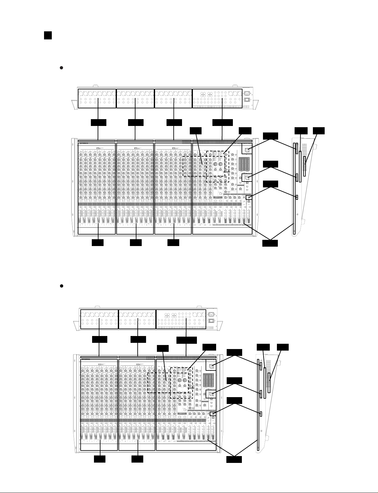
MG24/14FX
MG32/14FX
CIRCUIT BOARD LAYOUT
MG32/14FX
INJK INJK INJK
(INJK1) (INJK2) (INJK3)
(ユニットレイアウト)
MASJK
PS PSDSP DSP
MAS 2/4
MAS 3/4
MAS 4/4
MG24/14FX
IN IN IN(IN1) (IN2) (IN3) MAS
INJK INJK(INJK1) (INJK2)
MASJK
PS
MAS 1/4
PSDSP DSP
MAS 2/4
MAS 3/4
MAS 4/4
IN IN(IN1) (IN2)
MAS 1/4
17
Page 2
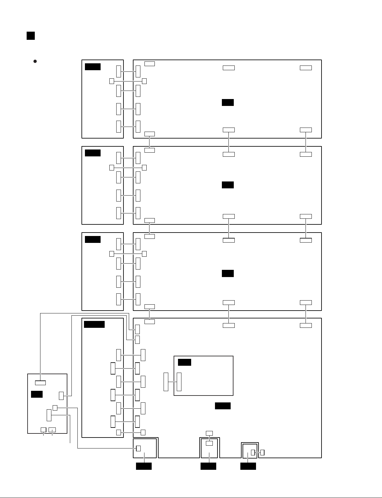
MG24/14FX
MG32/14FX
WIRING
MG32/14FX
(結線図)
INJK
(INJK1)
(INJK2)
CN101
CN105 CN105
CN102
1ch
~
8ch
CN103
CN104
INJK
CN101
CN105 CN105
CN102
9ch
~
16ch
CN103
CN104
CN101
CN102
CN103
CN104
CN101
CN102
CN103
CN104
CN107
CN106
CN107
CN106
IN
IN
CN108
(IN1)
CN109
CN108
(IN2)
CN109
CN110
CN111
CN110
CN111
PS
CN102
CN101
Transformer
CN103
CN104
CN105
CN100
AC-SW
Transformer
INJK
(INJK3)
CN101
CN105 CN105
CN102
17ch
~
24ch
CN103
CN104
MASJK
25ch
~
CN101
32ch
CN201
CN301
CN401
CN501
CN601
CN701
CN101
CN102
CN103
CN104
CN904
CN905
CN101
CN501
CN601
CN701
CN702
CN801
CN502
CN908
CN107
CN106
CN903
CN503
DSP
CN101
CN902
CN901
IN
MAS 1/4
CN108
CN110
(IN3)
CN109
CN301 CN302
CN907
CN906
CN111
18
MAS 2/4 MAS 3/4 MAS 4/4
Page 3
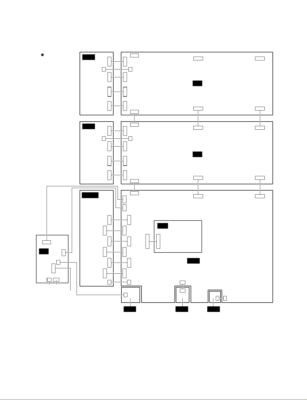
MG24/14FX
MG32/14FX
MG24/14FX
INJK
(INJK1)
(INJK2)
16ch
CN101
CN105 CN105
CN102
1ch
~
8ch
CN103
CN104
INJK
CN101
CN105 CN105
CN102
9ch
~
CN103
CN104
MASJK
CN101
CN102
CN103
CN104
CN101
CN102
CN103
CN104
CN904
CN905
CN107
CN106
CN107
CN106
CN903
CN108
(IN1)
IN
CN109
CN108
IN
(IN2)
CN109
CN301 CN302
CN110
CN111
CN110
CN111
PS
CN102
CN101
Transformer
CN103
CN104
CN105
CN100
AC-SW
Transformer
17ch
~
24ch
CN101
CN201
CN301
CN401
CN501
CN601
CN701
CN101
CN501
CN601
CN701
CN702
CN801
CN502
CN908
CN503
DSP
CN101
CN902
CN901
MAS 1/4
CN907
MAS 2/4 MAS 3/4 MAS 4/4
CN906
19
Page 4
MG24/14FX
MG32/14FX
1. Overview
(概観)
2
2
6
6
5
5
7
7
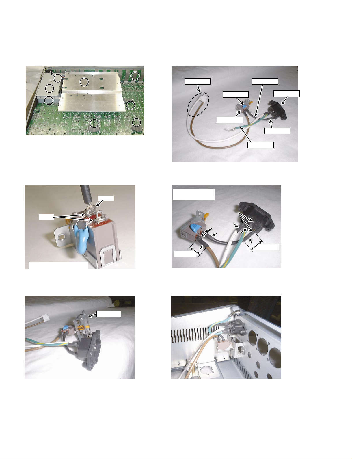
2-2. Detail of lead-wire treatment
two turn
4
4
3
3
3
3
(ワイヤー処理の詳細)
one turn
2-1.
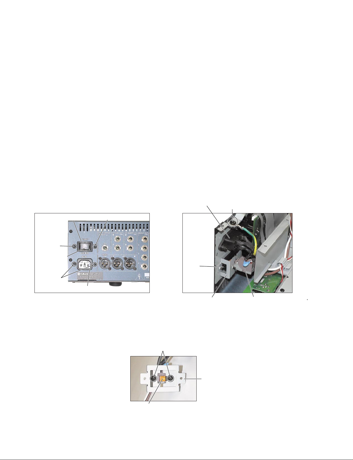
Assembly of AC-INLET & POWER-SW
260:WA609600
280:VV314800
3
3
230:VP184000
(ACインレット&PSWAss'y)
250: (WA60980)
190:WA782600
915:WB071100
270: (WA61030)
2-3. Solder and cover with heat-shrink-tube (five places)
(熱収縮チューブを備えた、ハンダおよびカバー(5箇所))
※ Cover firmly to a root.
(根元までしっかりカバー
をしてください)
※
※
(This picture is state of before soldering.)
(この写真は接合する前の状態です)
2-4. Set PS-HOLDER
(PSホルダーのセット)
210:WA677500
15mm ± 2mm
2-5. Set to Panel
15mm ± 2mm
(パネルへのセット)
20
Page 5
(MAS1000シートとIN1000シートの結線) (MASJK1000シートとINJK1000シートの結線)
3-1. Connect wire of circuit-board MAS1000 and IN1000 4-1. Connect wire of circuit-board MASJK1000 and INJK1000
430, 610:WB349600
420, 600:WB349700
80, 140:WB349800
90, 150:WB349900
4-2. Bend(forming) cable.
(屈曲(形成加工)ケーブル)
① MG32/14FX : 6 places, MG24/14FX : 4 places
CN301(MAS) – CN109(IN), CN108(IN) - CN109(IN),
CN302(MAS) - CN111(IN), CN110(IN) - CN111(IN)
② These four cables in left side.
(左側の4本のケーブル)
③ These four cables in right side.
(右側の4本のケーブル)
1
111
5-1.
Set CABLE-CLAMP (two places)
(CLAMPケーブルのセット(2箇所))
(トランスおよび珪素鋼板ボックスAss'y)
6-1. Assembly of TRANS and SILICON-STEEL-BOX
900:WA786300
905:VV104600
Bundle secondary wire of trans(トランスの第2ワイヤーの束)
X = 55mm ± 5mm
XYX
Y
Y = 65mm ± 5mm
20mm ± 5mm
Bundle Cable
·WA609600
·(WA69740)
MG24/14FX
MG32/14FX
21
Page 6
MG24/14FX
MG32/14FX
6-2.
Bundle secondary wire of trans and wire WA69740:PH-SAN-2P
(トランスおよびワイヤーWA69740:HP-SAN-2Pの第2ワイヤーの束) (シリコングリスを備えたPS1000シートおよびヒートシンクAss'y)
7-1.
Assembly of circuit-board PS1000 and HEAT-SINK with silicon grease.
heat-sink
830: (WA67590)
30mm ± 5mm
905:VV104600
7-2. Connect wire WA609600:VH-4P#18 - CN100
wire (WA69740) :PH-SAN-2P - CN105
primary wire of trans - CN101
secondary wire of trans - CN102
Bundle secondary wire of trans
and wire WA69740:PA-SAN-2P
(トランスおよびワイヤーWA69740:
PA-SAN-2Pの束の第2ワイヤー)
Twist two rotation and insert to connector.
(2つの回転を ねじり、コネクターに挿 入する)
910:WB327900
silicon grease
DB200,IC300,IC400,IC500,TR400,
IC200,IC201,IC202,IC203
7-3. Connect wire (WA60930):PH-SAN-11P - CN103
wire (WA60950):PH-SAN-6P - CN104
(シリコングリス)
7-4. Bundle by CABLE-CLAMP
22
(クランプケーブルによる束)
7-5. Set up
(セットアップ)
Page 7
MG24/14FX
MG32/14FX
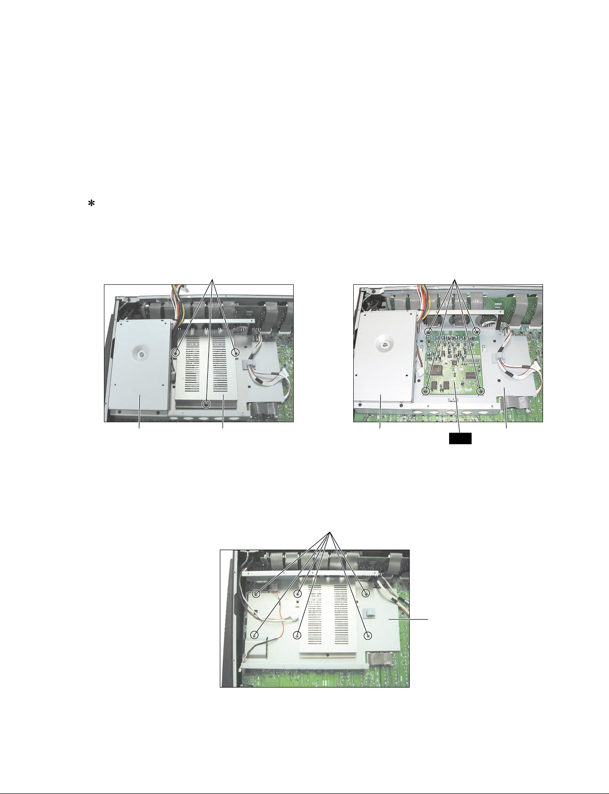
MG24/14FX DISASSEMBLY PROCEDURE
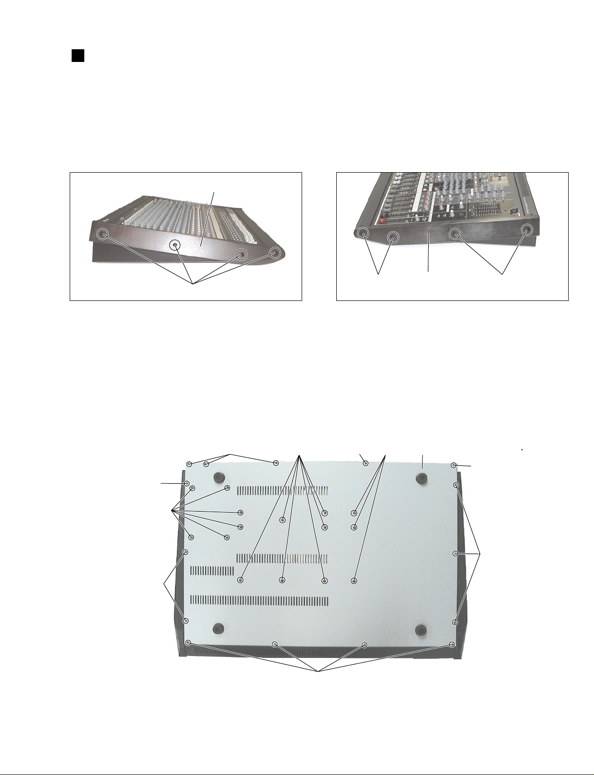
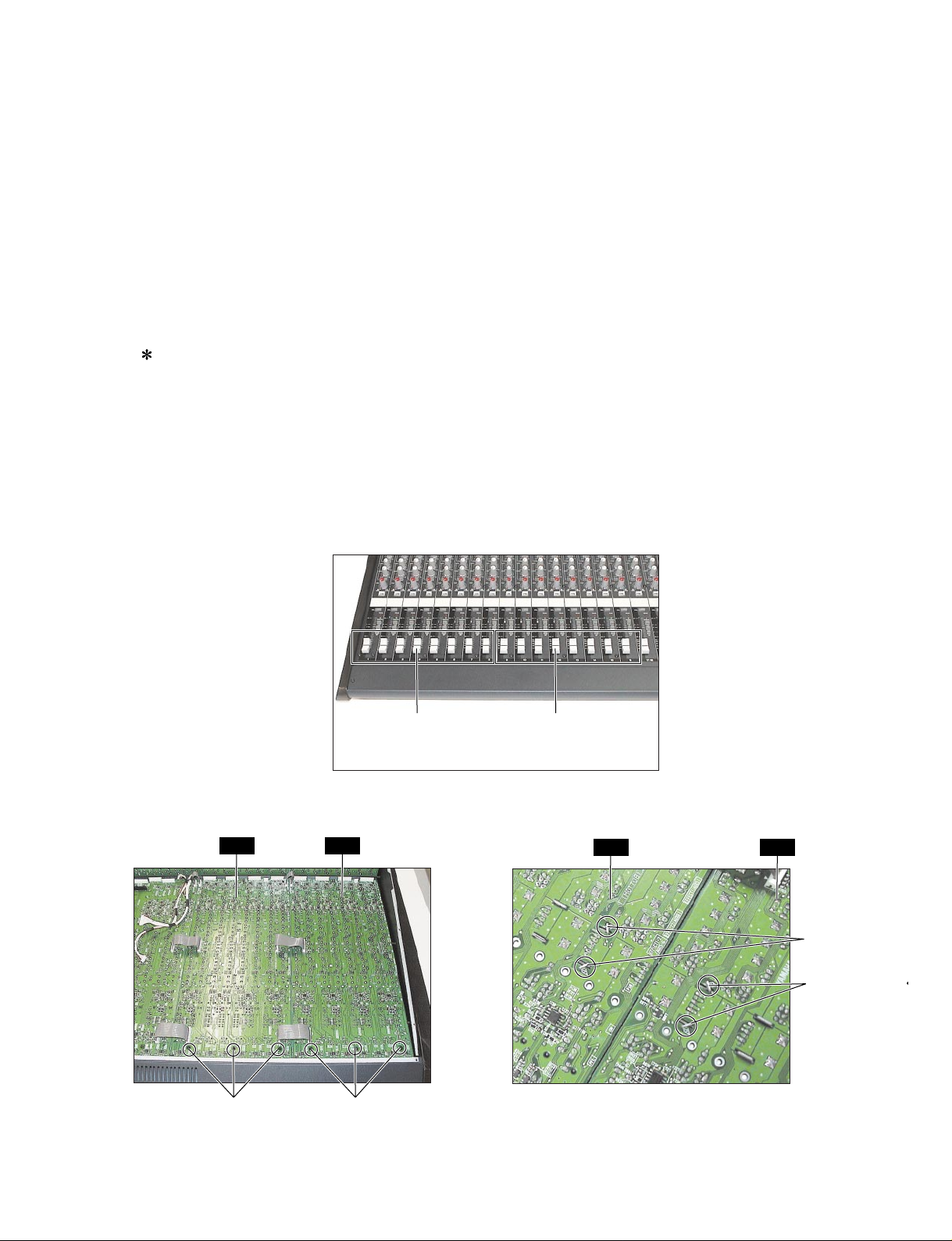
1. Side Pad (Time required: About 1 minute each)
1-1 Remove the four (4) screws marked [980]. Then,
remove the side pad L and flat washer. (Photo.1)
1-2 Remove the four (4) screws marked [1000]. Then,
remove the side pad R and flat washer. (Photo.2)
SidepadL(サイドパッドL)
[980]
[980]: Bind Head Tapping Screw-B
4.0X20 MFZN2BL (VS205900)
(+バインドBタイト)
1. サイドパッド(所要時間:各約 1 分)
1-1 [980]のネジ 4本を外し、サイドパッドL と平ワッ
1-2 [1000]のネジ4 本を外し、サイドパッドRと平ワッ
(MG24/14FX分解手順)
シャを外します。(写真1)
シャを外します。(写真2)
SidepadR
(サイドパッドR)
[1000]: Bind Head Tapping Screw-B
4.0X20 MFZN2BL (VS205900)
(+バインドBタイト)
[1000][1000]
Photo.1 (写真1)
2. Bottom Cover
(Time required: About 4 minutes)
2-1 Remove the fourteen (15) screws marked [930] and
the fifteen (15) screws marked [940]. Then, remove
the bottom cover. (Photo.3)
• Bottom view
[930]
[940]
[930]
[930] [930]
Photo.2 (写真2)
2. ボトムカバー(所要時間:約 4 分)
2-1 [930]のネジ 15本と[940]のネジ15 本を外し、ボト
ムカバーを外します。(写真3)
[940][940]
Bottomcover(ボトムカバー)
[930]
[930]
[930]
[930]: Bind Head Tapping Screw-S 3.0X6 MFZN2BL (VS205900)
[940]: Bind Head Tapping Screw-B 4.0X12 MFZN2BL (VR138400)
(+バインドSタイト)
(+バインドBタイト)
Photo.3 (写真3)
23
Page 8

MG24/14FX
MG32/14FX
3. Side Cover
(Time required: About 6 minutes each)
3-1 Remove the bottom cover. (See procedure 2.)
3-2 Side Cover L:
3-2-1 Remove the side pad L. (See procedure 1.)
3-2-2 Remove the five (5) hex socket set screws marked
[700] and the two (2) screws marked [710]. Then,
remove the side cover L. (Photo.4, 5)
3-3 Side Cover R:
3-3-1 Remove the side pad R. (See procedure 1.)
3-3-2 Remove the five (5) hex socket set screws marked
[730] and the two (2) screws marked [740]. Then,
remove the side cover R. (Photo.6, 7)
[700]
SidecoverL
(サイドカバーL)
3. サイドカバー(所要時間:各約 6 分)
3-1 ボトムカバーを外します。(2項参照)
3-2 サイドカバー L:
3-2-1 サイドパッド Lを外します。(1 項参照)
3-2-2 [700]の六角穴付きネジ5本と[710]のネジ 2 本を外
し、サイドカバー Lを外します。(写真 4、5)
3-3 サイドカバー R:
3-3-1 サイドパッド Rを外します。(1 項参照)
3-3-2 [730]の六角穴付きネジ5本と[740]のネジ 2 本を外
し、サイドカバー Rを外します。(写真 6、7)
[710]
[700]
[700]: Hex. Socket Set Screw
3.0X6 MFZN2BL (V9842300)
Photo.4 (写真4)
[730]: Hex. Socket Set Screw
3.0X6 MFZN2BL (V9842300)
(六角穴付きSタイト)
SidecoverR
(サイドカバーR)
[730]
(六角穴付きSタイト)
[730]
[710]: Bind Head Tapping Screw-S
3.0X6 MFZN2BL (EP630210)
Photo.5
[740]
[740]: Bind Head Tapping Screw-S
3.0X6 MFZN2BL (EP630210)
(写真5)
(+バインドSタイト)
(+バインドSタイト)
24
Photo.6 (写真6)
Photo.7
(写真7)
Page 9
MG24/14FX
MG32/14FX
4. Supports
4-1 When you work on the back of the top cov er , set the
supports to the right and left sides to prevent the
circuit boards from being distorted. (Photo.8)
Supports
(台)
Photo.8 (写真8)
4. 台
4-1 トップカバーの裏面の作業をする時、そのまま作業
すると基板がゆがんでしまうので、トップカバー裏
面の作業をする時は、左右に台を当ててください。
(写真 8)
5. PS Circuit Board
(Time required: About 6 minutes)
5-1 Remove the bottom cover. (See procedure 2.)
5-2 Set the supports. (See procedure 4.)
5-3 Remove the four (4) screws marked [865]. Remove
the PS circuit board and the heat sink. (Photo.9)
5-4 Remove the five (5) screws marked [840] and the
nine (9) screws marked [850]. Then, remov e the PS
circuit board from the heat sink. (Photo.11)
6. Power T ransformer
(Time required: About 6 minutes)
6-1 Remove the bottom cover. (See procedure 2.)
6-2 Set the supports. (See procedure 4.)
6-3 Remove the heat sink. (See procedure 5-3.)
6-4 Remove the four (4) screws marked [880]. Then,
remove the power tr ansformer with the silicon steel
plate box, silicon steel ring, trans spacer. (Photo.9)
6-5 Remove the bolt marked [A] and nut marked [B].
Then, remove the power transformer. (Photo.9, 10)
5. PS シート(所要時間:約 6 分)
5-1 ボトムカバーを外します。(2項参照)
5-2 台を当てます。(4項参照)
5-3 [865]のネジ4本を外し、PSシートとヒートシンク
を外します。(写真9)
5-4 [840]のネジ 5本と[850]のネジ9 本を外し、ヒート
シンクから PSシートを外します。(写真 11)
6. 電源トランス(所要時間:約6 分)
6-1 ボトムカバーを外します。(2項参照)
6-2 台を当てます。(4項参照)
6-3 ヒートシンクを外します。(5-3項参照)
6-4 [880]のネジ4本を外して、トランスベース、珪素鋼
板ボックス、珪素鋼板RING、トランススペーサー
と共に電源トランスを外します。(写真 9)
6-5 [A]のボルトと[B]のナットを外して、電源トランス
を外します。(写真 9、10)
25
Page 10

MG24/14FX
MG32/14FX
[880]
Bolt
(ボルト)
[A]
[880]
Transbase
(トランスベース)
[865]: Bind Head Tapping Screw-B
3.0X8 MFZN2BL (EP600190)
[880]: Bind Head Tapping Screw-B
3.0X8 MFZN2BL (EP600190)
Photo.9
[865]
Heatsink
(ヒートシンク)
(+バインドBタイト)
(+バインドBタイト)
(写真9)
[850]
Nut
(ナット)
[B]
SiliconSteelBox
(珪素鋼板ボックス)
Photo.10 (写真10)
PS
[840]
[840]: Bind Head Tapping Screw-B 3.0X8 MFZN2BL (EP600190)
[850]: Bind Head Tapping Screw-B 3.0X12 MFZN2BL (VQ074600)
Photo.11
7. DSP Circuit Board
(Time required: About 7 minutes)
7-1 Remove the bottom cover. (See procedure 2.)
7-2 Set the supports. (See procedure 4.)
7-3 Remove the heat sink. (See procedure 5-3.)
7-4 Remove the three (3) screws marked [800]. Remov e
the shield case. (Photo.12)
7-5 Remove the four (4) screws marked [780]. Then,
remove the DSP circuit board from the DSP shield
base. (Photo.13)
[840]
[850]
(+バインドBタイト)
(+バインドBタイト)
Heatsink
(ヒートシンク)
(写真11)
7. DSPシート(所要時間:約 7 分)
7-1 ボトムカバーを外します。(2項参照)
7-2 台を当てます。(4項参照)
7-3 ヒートシンクを外します。(5-3項参照)
7-4 [800]のネジ 3本を外し、シールドケースを外しま
す。(写真 12)
7-5 [780]のネジ 4本を外し、DSPシールドベースから
DSPシートを外します。(写真 13)
26
Page 11
MG24/14FX
MG32/14FX
8. DSP Shield Base
(Time required: About 7 minutes)
8-1 Remove the bottom cover. (See procedure 2.)
8-2 Set the supports. (See procedure 4.)
8-3 Remove the heat sink. (See procedure 5-3.)
8-4 Remove the trans base. (See procedure 6.)
8-5 Remove the six (6) screws marked [760]. Then,
remove the DSP shield base. (Photo.14)
At the time of DSP shield base attachment,
please tighten the screw of [760] after putting
the pin of the DSP sheet CN101 into CN503 of
MAS 1/4 sheet. (Photo. 14, 27, 28)
[800]
8. DSP シールドベース(所要時間:約 7 分)
8-1 ボトムカバーを外します。(2項参照)
8-2 台を当てます。(4項参照)
8-3 ヒートシンクを外します。(5-3項参照)
8-4 トランスベースを外します。(6項参照)
8-5 [760]のネジ 6本を外し、DSPシールドベースを外
します。(写真 14)
※DSPシールドベース取付時は、DSPシートCN101
のピンを MAS1/4 シートのCN503に入れてから
[760]のネジを締めてください。(写真14、27、28)
[780]
Transbase
(トランスベース)
[800]: Bind Head Tapping Screw-S
3.0X6 MFZN2BL (EP630210)
Photo.12
Shieldcase
(シールドケース)
(写真12)
(+バインドSタイト)
[760]: Bind Head Tapping Screw-S
3.0X8 MFZN2BL (EP600530)
Transbase
(トランスベース)
[780]: Bind Head Tapping Screw-S
[760]
(+バインドSタイト)
DSP
3.0X6 MFZN2BL (EP630210)
Photo.13
(写真13)
DSPshieldbase
(DSPシールドベース)
DSPshieldbase
(DSPシールドベース)
(+バインドSタイト)
Photo.14
(写真14)
27
Page 12
MG24/14FX
AC-INconnector
MG32/14FX
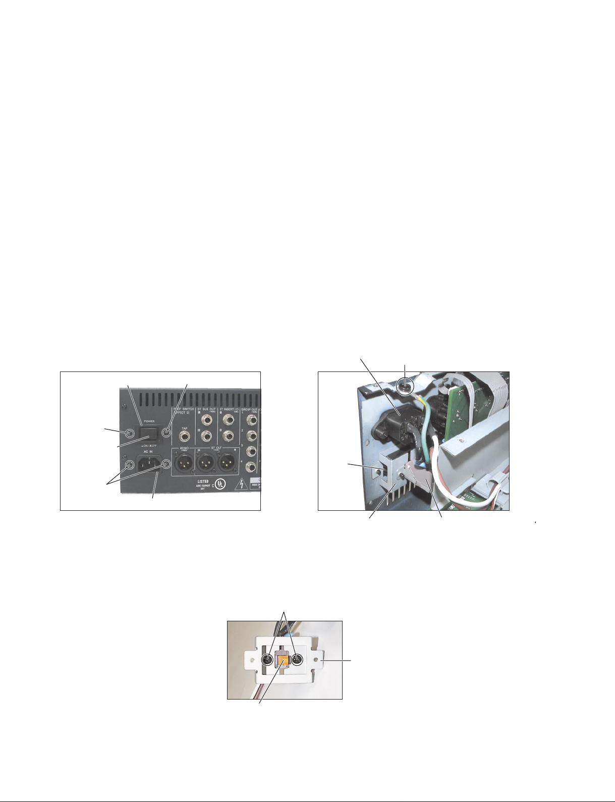
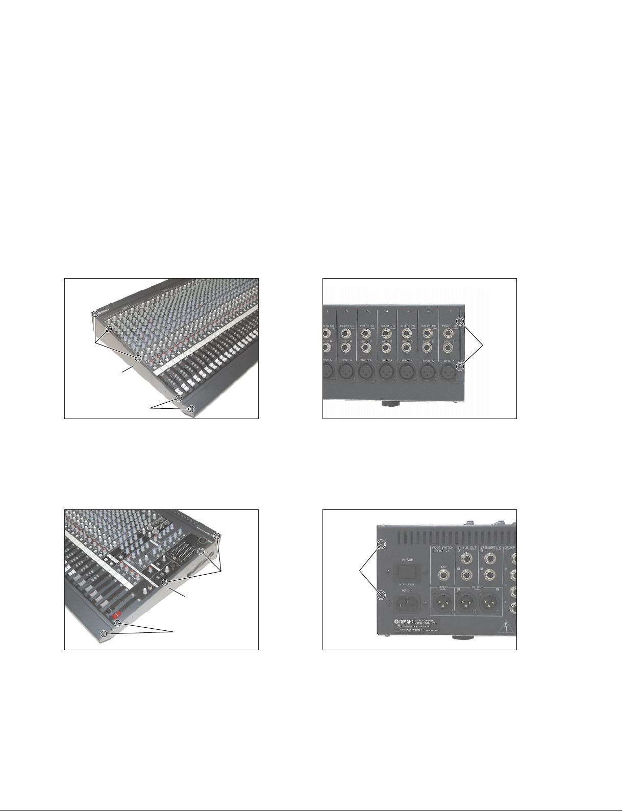
9. Push Switch and AC-IN Connector
(Time required: About 6 minutes)
9-1 Remove the bottom cover. (See procedure 2.)
9-2 Set the supports. (See procedure 4.)
9-3 Remove the heat sink. (See procedure 5-3.)
9-4 Remove the trans base. (See procedure 6.)
9-5 Remove the two (2) screws marked [200]. (Photo .15, 16)
9-6 Remove the power switch escutcheon by bending the
claw of the power switch escutcheon. (Photo.15, 16)
9-7 Remove the power switch knob. Remove the two
(2) screws marked [240]. Then, remove the push
switch from the PS holder. (Photo.17)
10. Push Switch and AC-IN Connector
(Time required: About 5 minutes)
10-1 Remove the bottom cover. (See procedure 2.)
10-2 Set the supports. (See procedure 4.)
10-3 Remove the two (2) screws marked [220] and a
screw marked [310]. Remove the A C-IN connector.
(Photo.15, 16)
Powerswitchescutcheon
(PSWエス
カッション)
[200]
9. プッシュ SW(所要時間:約 6 分)
9-1 ボトムカバーを外します。(2項参照)
9-2 台を当てます。(4項参照)
9-3 ヒートシンクを外します。(5-3項参照)
9-4 トランスベースを外します。(6項参照)
9-5 [200]のネジ 2本を外します。(写真 15、16)
9-6 PSW エスカッションのツメを曲げて、PSW エス
カッションを外します。(写真 15、16)
9-7 PSW ノブを外し、[240]のネジ 2 本を外し、PSホル
ダーからプッシュ SWを外します。(写真 17)
10. ACインレット(所要時間:約 5 分)
10-1 ボトムカバーを外します。(2 項参照)
10-2 台を当てます。(4 項参照)
10-3 [220]のネジ2本と[310]のネジ1本を外し、ACイン
レットを外します。(写真 15、16)
(ACインレット)
[310]
[200]
Powerswitch
knob
(PSWノブ)
[220]
AC-INconnector
[200]: Bind Head Tapping Screw-B
3.0X12 MFZN2BL (VQ074600)
[220]: Bind Head Tapping Screw-S
3.0X6 MFZN2BL (EP630210)
Photo.15
(写真15)
(ACインレット)
(+バインドBタイト)
(+バインドSタイト)
[240]
Pushswitch
(プッシュSW)
Claw
(ツメ)
PSholder
(PSホルダー)
[310]: Bind Head Screw A4.0X8 MFZN2BL (VP156800)
(+バインドBタイト)
Photo.16
PSholder
(PSホルダー)
Pushswitch
(写真16)
(プッシュSW)
28
[240]: Bind Head Tapping Screw-S 3.0X6 MFZN2BL (EP630210)
(+バインドSタイト)
Photo.17
(写真17)
Page 13
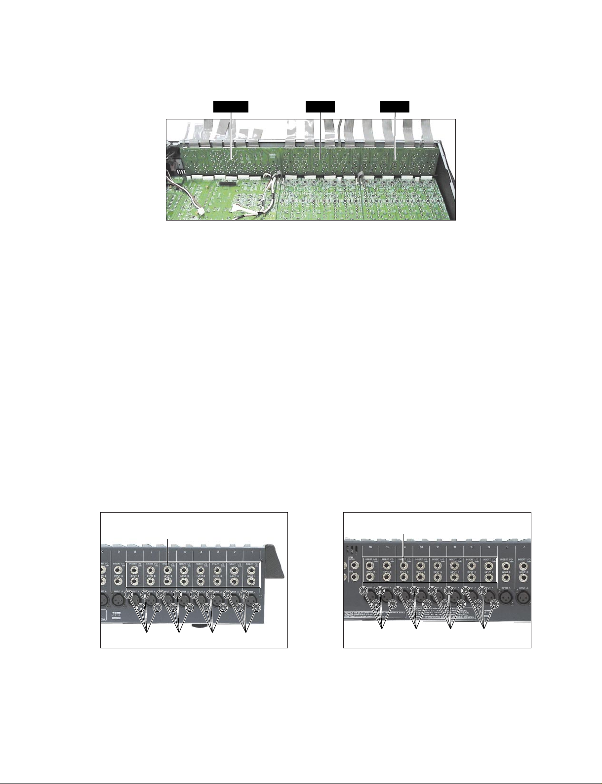
Photo.18(写真18)
MG24/14FX
MG32/14FX
INJK 1INJK 2MASJK
11. INJK Circuit Boards 1 and 2
11-1 Remove the bottom cover. (See procedure 2.)
11-2 Set the supports. (See procedure 4.)
11-3 INJK Circuit Board 1:
(Time required: About9 minutes)
11-3-1 Remove the side pad L. (See procedure 1.)
11-3-2 Remove the sixteen (16) screws marked [100A] and
the sixteen (16) hexagonal nuts and flat washer
marked [A]. Then, remove the INJK circuit board 1.
(Photo.18, 19)
11-4 INJK Circuit Board 2:
(Time required: About 10 minutes)
11-4-1 Remove the heat sink. (See procedure 5-3.)
11-4-2 Remove the sixteen (16) screws marked [100B] and
the sixteen (16) hexagonal nuts and flat washer
marked [B]. Then, remove the INJK circuit board 2.
(Photo.18, 20)
Hexagonalnutandflatwasher[A]
(特殊六角ナットと平ワッシャ[A])
11. INJK シート 1、2
11-1 ボトムカバーを外します。(2 項参照)
11-2 台を当てます。(4 項参照)
11-3 INJKシート 1:(所要時間:約9分)
11-3-1 サイドパッド L を外します。(1 項参照)
11-3-2 [100A]のネジ16本と[A]の特殊六角ナットと平ワッ
シャ各 16個を外し、INJKシート 1 を外します。
(写真 18、19)
11-4 INJKシート 2:(所要時間:約10分)
11-4-1 ヒートシンクを外します。(5-3項参照)
11-4-2 [100B]のネジ16本と[B]の特殊六角ナットと平ワッ
シャ各 16個を外し、INJKシート 2 を外します。
(写真 18、20)
Hexagonalnutandflatwasher[B]
(特殊六角ナットと平ワッシャ[B])
[100]: Bonding Tapping Screw-B
3.0X8 MFZN2BL (VN413300)
Photo.19
(写真19)
[100A][100A][100A][100A]
(ボンディングBタイト)
[100]: Bonding Tapping Screw-B
3.0X8 MFZN2BL (VN413300)
Photo.20
(写真20)
[100B][100B][100B][100B]
(ボンディングBタイト)
29
Page 14
MG24/14FX
MG32/14FX
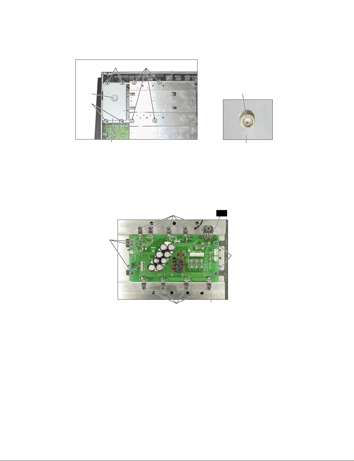
12. MASJK Circuit Board
(Time required: About 11 minutes)
12-1 Remove the bottom cover. (See procedure 2.)
12-2 Set the supports. (See procedure 4.)
12-3 Remove the heat sink. (See procedure 5-3.)
12-4 Remove the trans base. (See procedure 6.)
12-5 Remove the DSP shield base. (See procedure 8.)
12-6 Remove the eight (8) screws marked [160] and the
thirty-three (33) hexagonal nuts and flat washer
marked [C]. Then, remove the MASJK circuit board.
(Photo.18, 21)
At the time of DSP shield base attachment,
please tighten the screw of [760] after putting
the pin of the DSP sheet CN101 into CN503 of
MAS 1/4 sheet. (Photo. 14, 27, 28)
Hexagonalnut[C]
12. MASJKシート(所要時間:約 11 分)
12-1 ボトムカバーを外します。(2 項参照)
12-2 台を当てます。(4 項参照)
12-3 ヒートシンクを外します。(5-3 項参照)
12-4 トランスベースを外します。(6 項参照)
12-5 DSPシールドベースを外します。(8 項参照)
12-6 [160]のネジ8本と[C]の特殊六角ナットと平ワッ
シャ各 33個を外し、MASJKシートを外します。
(写真 18、21)
※DSPシールドベース取付時は、DSPシートCN101
のピンをMAS1/4 シートのCN503に入れてから
[760]のネジを締めてください。(写真14、27、28)
(特殊六角ナット[C])
[160]
[160]
[160]: Bonding Tapping Screw-B 3.0X8 MFZN2BL (VN413300)
(ボンディングBタイト)
Photo.21
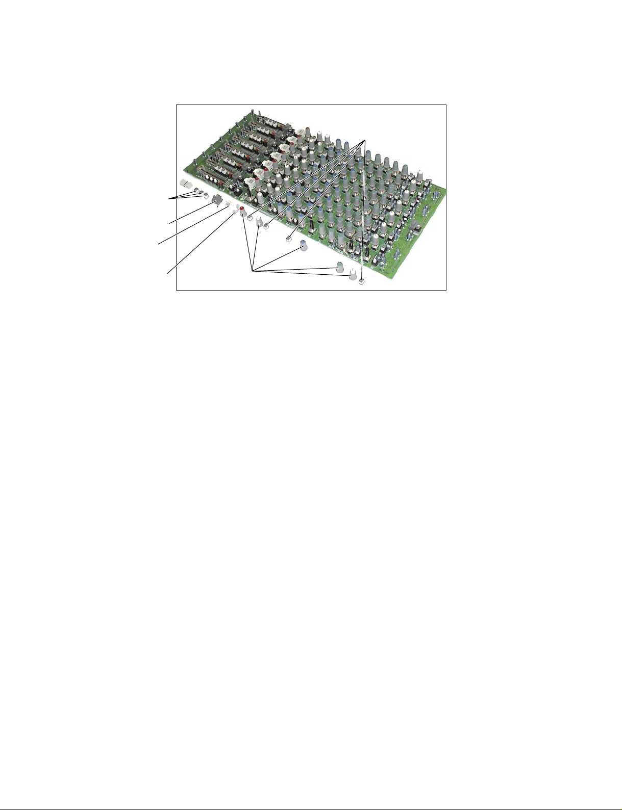
13. IN Circuit Boards 1 and 2
13-1 Remove the bottom cover. (See procedure 2.)
13-2 Set the supports. (See procedure 4.)
13-3 IN Circuit Board 1:
(Time required: About 9 minutes)
13-3-1 Remove the side pad L. (See procedure 1.)
13-3-2 Remove the eight (8) fader knobs 1. (Photo.22)
13-3-3 Remove the three (3) screws marked [590A].
(Photo.23)
13-3-4 T wist the eighteen (18) hooks of the IN circuit board
1 to become straight. Then, remove the IN circuit
board 1.(Photo.24)
[160]
(写真21)
13. IN シート 1、2
13-1 ボトムカバーを外します。(2 項参照)
13-2 台を当てます。(4 項参照)
13-3 INシート 1:(所要時間:約9分)
13-3-1 サイドパッド L を外します。(1 項参照)
13-3-2 ノブ(FADER1)8 個を外します。(写真22)
13-3-3 [590A]のネジ 3 本を外します。(写真 23)
13-3-4 IN シート1を固定しているフック18箇所をまっす
ぐになるようにひねり、INシート1 を外します。
(写真 24)
30
Page 15
MG24/14FX
MG32/14FX
13-4 IN Circuit Board 2:
(Time required: About 10 minutes)
13-4-1 Remove the eight (8) fader knobs 2. (Photo.22)
13-4-2 Remove the heat sink. (See procedure 5-3.)
13-4-3 Remove the DSP shield base. (See procedure 8.)
13-4-3 Remove the three (3) screws marked [590B].
(Photo.23)
13-4-4 T wist the eighteen (18) hooks of the IN circuit board
2 to become straight. Then, remove the IN circuit
board 2.(Photo.24)
The push ON buttons, sleeve ON buttons, push
PFL buttons, volume knobs, and push HPF
buttons on the IN circuit boards 1 and 2 are not
components of the circuit board. When you
replace the IN circuit board, you should r emove
the push ON buttons, sleeve ON buttons, push
PFL buttons, volume knobs, and push HPF
buttons from the old IN circuit boards 1 and 2,
and install them in the new circuit board.
(Photo.25)
13-4 INシート 2:(所要時間:約10 分)
13-4-1 ノブ(FADER2)8 個を外します。(写真22)
13-4-2 ヒートシンクを外します。(5-3項参照)
13-4-3 DSP シールドベースを外します。(8 項参照)
13-4-3 [590B]のネジ 3 本を外します。(写真 23)
13-4-4 IN シート2を固定しているフック18箇所をまっす
ぐになるようにひねり、IN シート2を外します。
(写真 24)
※INシート 1、 2上のボタンONAssy、 スリーブON
ボタン、ボタンPFL、ノブ(VR)、ボタンHPF は、
INシート1、2の構成部品ではありません。INシー
トを交換する際には、INシート1、2からボタンON
Assy、スリーブONボタン、ボタンPFL、ノブ(VR)、
ボタン HPFを取り外して、新しいIN シート 1、2
に取り付けてください。(写真25)
[590]: Bind Head Tapping Screw-S
3.0X6 MFZN2BL (EP630210)
Faderknob1x8
(ノブ(FADER1))
IN 1IN 2
[590A][590B]
(+バインドSタイト)
Faderknob2x8
(ノブ(FADER2))
Photo.22(写真22)
IN 1IN 2
Hooks(フック)
Hooks(フック)
Photo.24(写真24)
Photo.23
(写真23)
31
Page 16
MG24/14FX
MG32/14FX
PushHPFbuttons
(ボタンHPF)
PushPFLbuttons
(ボタンPFL)
PushONbuttons
(ボタンONAss'y)
SleeveONbuttons
(スリーブONボタン)
PushHPFbuttons
(ボタンHPF)
Volumeknob
(ノブ(VR))
Photo.25(写真25)
14. MAS 1/4 to 4/4 Circuit Boards
(Time required: About 15 minutes)
14-1 Remove the bottom cover. (See procedure 1.)
14-2 Set the supports. (See procedure 4.)
14-3 Remove the heat sink. (See procedure 5-3.)
14-4 Remove the DSP shield base. (See procedure 8.)
14-5 MAS 2/4: (Time required: About 7 minutes)
14-5-1 Remove the two (2) screws marked [390A] from the
control panel surface. Then, remove the MAS 2/4
circuit board. (Photo.26, 29)
14-6 MAS 3/4: (Time required: About 7 minutes)
14-6-1 Remove the two (2) screws marked [390B] from the
control panel surface. Then, remove the MAS 3/4
circuit board. (Photo.26, 29)
14-7 MAS 4/4: (Time required: About 7 minutes)
14-7-1 Remove the hexagonal nut and flat washer [D] from
the control panel surface.Then, remov e the MAS 4/4
circuit board. (Photo.26, 29, 30)
14-8 MAS 1/4: (Time required: About 12 minutes)
14-8-1 Remove the side pad R. (See procedure 1.)
14-8-2 Remove the twelve (12) f ader knobs and the two (2)
select knobs from the control panel surface.
(Photo.26)
14-8-3 Remove the MAS 2/4 circuit board.
(See procedure 14-5.)
14-8-4 Remove the MAS 3/4 circuit board.
(See procedure 14-6.)
14-8-5 Remove the MAS 4/4 circuit board.
(See procedure 14-7.)
14-8-6 Remove the four (4) screws marked [380]. (Photo .29)
14-8-7 Twist the twenty-four (24) hooks of the MAS 1/4
circuit board to become straight. Then, remove the
MAS 1/4, 3/4, and 4/4 circuit boards. (Photo.29)
14. MAS1/4 〜 4/4 シート
14-1 ボトムカバーを外します。(1 項参照)
14-2 台を当てます。(4 項参照)
14-3 ヒートシンクを外します。(5-3 項参照)
14-4 DSPシールドベースを外します。(8 項参照)
14-5 MAS2/4:(所要時間:約 7分)
14-5-1 コントロールパネル面から、[390A]のネジ2本を外
して、MAS2/4シートを外します。(写真 26、29)
14-6 MAS3/4:(所要時間:約 7分)
14-6-1 コントロールパネル面から、[390B]のネジ2本を外
し、MAS3/4シートを外します。(写真 26、29)
14-7 MAS4/4:(所要時間:約 7分)
14-7-1 [D]の特殊六角ナットと平ワッシャ1個を外し、MAS
4/4 シートと基板固定金具を外します。
(写真26、29、30)
14-8 MAS1/4:(所要時間:約 12分)
14-8-1 サイドパッド R を外します。(1 項参照)
14-8-2 コントロールパネル面から、ノブ(FADER)12個と
ノブ(SELECT)2個を外します。(写真 26)
14-8-3 MAS2/4 シートを外します。(14-5 項参照)
14-8-4 MAS3/4 シートを外します。(14-6 項参照)
14-8-5 MAS4/4 シートを外します。(14-7 項参照)
14-8-6 [380]のネジ 4 本を外します。(写真 29)
14-8-7 MAS1/4 シートを固定しているフック 24 箇所を
まっすぐになるようにひねり、MAS1/4 シートを
外します。(写真 29)
32
Page 17

MG24/14FX
MG32/14FX
The meter reflector, push ON buttons, sleeve ON
buttons, push PFL buttons, holder circuit board,
volume knobs, push HPF buttons, push TAP
buttons, and meter cover, push spacer on the
MAS 1/4 circuit board are not components of
the circuit board. When you replace the MAS 1/
4 circuit board, you should remove the meter
reflector, push ON buttons, sleeve ON buttons,
push PFL buttons, holder circuit board, volume
knobs, push HPF buttons, push T AP buttons, and
meter cover, push spacer from the old MAS 1/4
circuit board, and install in the new circuit boar d.
(Photo.30)
At the time of DSP shield base attachment,
please tighten the screw of [760] after putting
the pin of the DSP sheet CN101 into CN503 of
MAS 1/4 sheet. (Photo. 14, 27, 28)
※MAS1/4シート上のリフレクターMETER、ボタン
ONAssy、スリーブ ONボタン、ボタンPFL、基
板固定金具、ノブ(VR)、ボタンHPF、ボタンTAP、
ウインドウMETER、プッシュスペーサーは、MAS
1/4 シートの構成部品ではありません。MA S 1 / 4
シートを交換する際には、MAS1/4 シートからリ
フレクターMETER、ボタンONAssy、スリーブ
ONボタン、ボタンPFL、基板固定金具、ノブ(VR)、
ボタンHPF、ボタンTAP、ウインドウMETER、プッ
シュスペーサーを取り外して、新しいMAS1/4シー
トに取り付けてください。(写真 30)
※DSPシールドベース取付時は、DSPシートCN101
のピンを MAS1/4 シートのCN503に入れてから
[760]のネジを締めてください。(写真14、27、28)
Selectknob
(ノブ(SELECT))
[390A]
[390B]
DSP:CN101
Photo.27 (写真27)
Hexagonalnut
andflatwasher[D]
(特殊六角ナットと
平ワッシャ[D])
Faderknob
(ノブ(FADER))
[390]: Bonding Tapping Screw-B 3.0X8 MFZN2BL (VN413300)
(ボンディングBタイト)
Photo.26 (写真26)
DSPshieldbase
(DSPシールドベース)
MAS 1/4
Photo.28 (写真28)
MAS1/4:CN503
33
Page 18

MG24/14FX
MG32/14FX
MAS 2/4MAS 3/4MAS 4/4MAS 1/4
[380]
PushONbuttons
(ボタンONAss'y)
PushPFLbuttons
(ボタンPFL)
PushHPFbuttons
(ボタンHPF)
Volumeknob
PushTAPbuttons
(ボタンTAP)
(ノブ(VR))
Photo.29 (写真29)
MAS 1/4
Photo.30 (写真30)
Hooks x24
(フック)
Metercover
(ウインドウMETER)
MAS 3/4
TootheLockWasher
(歯付座金)
Holder,circuitboard
MAS 4/4
(基板固定金具)
Meterreflector
(リフレクターMETER)
34
Page 19

MG24/14FX
MG32/14FX
MG32/14FX DISASSEMBLY PROCEDURE
1. Side Pad (Time required: About 1 minute each)
1-1 Remove the four (4) screws marked [980]. Then,
remove the side pad L and flat washer. (Photo.1)
1-2 Remove the four (4) screws marked [1000]. Then,
remove the side pad R and flat washer. (Photo.2)
SidepadL(サイドパッドL)
[980]
[980]: Bind Head Tapping Screw-B
4.0X20 MFZN2BL (VS205900)
(+バインドBタイト)
1. サイドパッド(所要時間:各約 1 分)
1-1 [980]のネジ 4本を外し、サイドパッドL と平ワッ
1-2 [1000]のネジ4 本を外し、サイドパッドRと平ワッ
(MG32/14FX分解手順)
シャを外します。(写真 1)
シャを外します。(写真 2)
SidepadR
(サイドパッドR)
[1000]: Bind Head Tapping Screw-B
4.0X20 MFZN2BL (VS205900)
(+バインドBタイト)
[1000][1000]
Photo.1 (写真1)
2. Bottom Cover
(Time required: About 4 minutes)
2-1 Remove the sixteen (17) screws marked [930] and
the fifteen (15) screws marked [940]. Then, remove
the bottom cover. (Photo.3)
• Bottom view
[930]
[940]
[930]
[930] [930]
Photo.2 (写真2)
2. ボトムカバー(所要時間:約 4 分)
2-1 [930]のネジ 17本と[940]のネジ15 本を外し、ボト
ムカバーを外します。(写真 3)
[940][940]
Bottomcover(ボトムカバー)
[930]
[930]
[930]
[930]: Bind Head Tapping Screw-S 3.0X6 MFZN2BL (VS205900)
[940]: Bind Head Tapping Screw-B 4.0X12 MFZN2BL (VR138400)
(+バインドSタイト)
(+バインドBタイト)
Photo.3 (写真3)
35
Page 20
MG24/14FX
MG32/14FX
3. Side Cover
(Time required: About 6 minutes each)
3-1 Remove the bottom cover. (See procedure 2.)
3-2 Side Cover L:
3-2-1 Remove the side pad L. (See procedure 1.)
3-2-2 Remove the five (5) hex socket set screws marked
[700] and the two (2) screws marked [710]. Then,
remove the side cover L. (Photo.4, 5)
3-3 Side Cover R:
3-3-1 Remove the side pad R. (See procedure 1.)
3-3-2 Remove the five (5) hex socket set screws marked
[730] and the two (2) screws marked [740]. Then,
remove the side cover R. (Photo.6, 7)
[700]
SidecoverL
(サイドカバーL)
3. サイドカバー(所要時間:各約 6 分)
3-1 ボトムカバーを外します。(2項参照)
3-2 サイドカバー L:
3-2-1 サイドパッド Lを外します。(1 項参照)
3-2-2 [700]の六角穴付きネジ5本と[710]のネジ 2 本を外
し、サイドカバー Lを外します。(写真 4、5)
3-3 サイドカバー R:
3-3-1 サイドパッド Rを外します。(1 項参照)
3-3-2 [730]の六角穴付きネジ5本と[740]のネジ 2 本を外
し、サイドカバー Rを外します。(写真 6、7)
[710]
[700]
[700]: Hex. Socket Set Screw
3.0X6 MFZN2BL (V9842300)
Photo.4 (写真4)
[730]: Hex. Socket Set Screw
3.0X6 MFZN2BL (V9842300)
(六角穴付きSタイト)
[730]
SidecoverR
(サイドカバーR)
[730]
(六角穴付きSタイト)
[710]: Bind Head Tapping Screw-S
3.0X6 MFZN2BL (EP630210)
Photo.5
[740]
[740]: Bind Head Tapping Screw-S
3.0X6 MFZN2BL (EP630210)
(写真5)
(+バインドSタイト)
(+バインドSタイト)
36
Photo.6 (写真6)
Photo.7
(写真7)
Page 21

MG24/14FX
MG32/14FX
4. Supports
4-1 When you work on the back of the top cov er , set the
supports to the right and left sides to prevent the
circuit boards from being distorted. (Photo.8)
Supports
(台)
Photo.8 (写真8)
4. 台
4-1 トップカバーの裏面の作業をする時、そのまま作業
すると基板がゆがんでしまうので、トップカバー裏
面の作業をする時は、左右に台を当ててください。
(写真 8)
5. PS Circuit Board
(Time required: About 6 minutes)
5-1 Remove the bottom cover. (See procedure 2.)
5-2 Set the supports. (See procedure 4.)
5-3 Remove the four (4) screws marked [865]. Remove
the PS circuit board and the heat sink. (Photo.9)
5-4 Remove the five (5) screws marked [840] and the
nine (9) screws marked [850]. Then, remov e the PS
circuit board from the heat sink. (Photo.11)
6. Power T ransformer
(Time required: About 6 minutes)
6-1 Remove the bottom cover. (See procedure 2.)
6-2 Set the supports. (See procedure 4.)
6-3 Remove the heat sink. (See procedure 5-3.)
6-4 Remove the four (4) screws marked [880]. Then,
remove the power tr ansformer with the silicon steel
plate box, silicon steel ring, trans spacer. (Photo.9)
6-5 Remove the bolt marked [A] and nut marked [B].
Then, remove the power transformer. (Photo.9, 10)
5. PS シート(所要時間:約 6 分)
5-1 ボトムカバーを外します。(2項参照)
5-2 台を当てます。(4項参照)
5-3 [865]のネジ4本を外し、PSシートとヒートシンク
を外します。(写真 9)
5-4 [840]のネジ 5本と[850]のネジ9 本を外し、ヒート
シンクから PSシートを外します。(写真 11)
6. 電源トランス(所要時間:約6 分)
6-1 ボトムカバーを外します。(2項参照)
6-2 台を当てます。(4項参照)
6-3 ヒートシンクを外します。(5-3項参照)
6-4 [880]のネジ4本を外して、トランスベース、珪素鋼
板ボックス、珪素鋼板RING、トランススペーサー
と共に電源トランスを外します。(写真 9)
6-5 [A]のボルトと[B]のナットを外して、電源トランス
を外します。(写真 9、10)
37
Page 22
MG24/14FX
MG32/14FX
[880]
Bolt
(ボルト)
[A]
[880]
Transbase
(トランスベース)
[865]: Bind Head Tapping Screw-B
3.0X8 MFZN2BL (EP600190)
[880]: Bind Head Tapping Screw-B
3.0X8 MFZN2BL (EP600190)
Photo.9
[865]
Heatsink
(ヒートシンク)
(+バインドBタイト)
(+バインドBタイト)
(写真9)
[850]
Nut
(ナット)
[B]
SiliconSteelBox
(珪素鋼板ボックス)
Photo.10 (写真10)
PS
[840]
[840]: Bind Head Tapping Screw-B 3.0X8 MFZN2BL (EP600190)
[850]: Bind Head Tapping Screw-B 3.0X12 MFZN2BL (VQ074600)
Photo.11
7. DSP Circuit Board
(Time required: About 7 minutes)
7-1 Remove the bottom cover. (See procedure 2.)
7-2 Set the supports. (See procedure 4.)
7-3 Remove the heat sink. (See procedure 5-3.)
7-4 Remove the three (3) screws marked [800]. Remov e
the shield case. (Photo.12)
7-5 Remove the four (4) screws marked [780]. Then,
remove the DSP circuit board from the DSP shield
base. (Photo.13)
[840]
[850]
(+バインドBタイト)
(+バインドBタイト)
Heatsink
(ヒートシンク)
(写真11)
7. DSPシート(所要時間:約 7 分)
7-1 ボトムカバーを外します。(2項参照)
7-2 台を当てます。(4項参照)
7-3 ヒートシンクを外します。(5-3項参照)
7-4 [800]のネジ 3本を外し、シールドケースを外しま
す。(写真 12)
7-5 [780]のネジ 4本を外し、DSPシールドベースから
DSPシートを外します。(写真 13)
38
Page 23

MG24/14FX
MG32/14FX
8. DSP Shield Base
(Time required: About 7 minutes)
8-1 Remove the bottom cover. (See procedure 2.)
8-2 Set the supports. (See procedure 4.)
8-3 Remove the heat sink. (See procedure 5-3.)
8-4 Remove the trans base. (See procedure 6.)
8-5 Remove the six (6) screws marked [760]. Then,
remove the DSP shield base. (Photo.14)
At the time of DSP shield base attachment,
please tighten the screw of [760] after putting
the pin of the DSP sheet CN101 into CN503 of
MAS 1/4 sheet. (Photo. 14, 28, 39)
[800]
8. DSP シールドベース(所要時間:約 7 分)
8-1 ボトムカバーを外します。(2項参照)
8-2 台を当てます。(4項参照)
8-3 ヒートシンクを外します。(5-3項参照)
8-4 トランスベースを外します。(6項参照)
8-5 [760]のネジ 6本を外し、DSPシールドベースを外
します。(写真 14)
※DSPシールドベース取付時は、DSPシートCN101
のピンを MAS1/4 シートのCN503に入れてから
[760]のネジを締めてください。(写真14、28、29)
[780]
Transbase
(トランスベース)
[800]: Bind Head Tapping Screw-S
3.0X6 MFZN2BL (EP630210)
Photo.12
Shieldcase
(シールドケース)
(写真12)
(+バインドSタイト)
[760]: Bind Head Tapping Screw-S
3.0X8 MFZN2BL (EP600530)
Transbase
(トランスベース)
[780]: Bind Head Tapping Screw-S
[760]
(+バインドSタイト)
DSP
3.0X6 MFZN2BL (EP630210)
Photo.13
(写真13)
DSPshieldbase
(DSPシールドベース)
DSPshieldbase
(DSPシールドベース)
(+バインドSタイト)
Photo.14
(写真14)
39
Page 24
MG24/14FX
AC-INconnector
MG32/14FX
9. Push Switch and AC-IN Connector
(Time required: About 6 minutes)
9-1 Remove the bottom cover. (See procedure 2.)
9-2 Set the supports. (See procedure 4.)
9-3 Remove the heat sink. (See procedure 5-3.)
9-4 Remove the trans base. (See procedure 6.)
9-5 Remove the two (2) screws marked [200]. (Photo .15, 16)
9-6 Remove the power switch escutcheon by bending the
claw of the power switch escutcheon. (Photo.15, 16)
9-7 Remove the power switch knob. Remove the two
(2) screws marked [240]. Then, remove the push
switch from the PS holder. (Photo.17)
10. Push Switch and AC-IN Connector
(Time required: About 5 minutes)
10-1 Remove the bottom cover. (See procedure 2.)
10-2 Set the supports. (See procedure 4.)
10-3 Remove the two (2) screws marked [220] a screw
marked [310]. Remove the AC-IN connector.
(Photo.15, 16)
Powerswitchescutcheon
(PSWエス
カッション)
[200]
9. プッシュ SW(所要時間:約 6 分)
9-1 ボトムカバーを外します。(2項参照)
9-2 台を当てます。(4項参照)
9-3 ヒートシンクを外します。(5-3項参照)
9-4 トランスベースを外します。(6項参照)
9-5 [200]のネジ 2本を外します。(写真 15、16)
9-6 PSW エスカッションのツメを曲げて、PSW エス
カッションを外します。(写真 15、16)
9-7 PSW ノブを外し、[240]のネジ 2 本を外し、PSホル
ダーからプッシュ SWを外します。(写真 17)
10. ACインレット(所要時間:約 5 分)
10-1 ボトムカバーを外します。(2 項参照)
10-2 台を当てます。(4 項参照)
10-3 [220]のネジ2本と[310]のネジ1本を外し、ACイン
レットを外します。(写真 15、16)
(ACインレット)
[310]
[200]
Powerswitch
knob
(PSWノブ)
[220]
AC-INconnector
[200]: Bind Head Tapping Screw-B
3.0X12 MFZN2BL (VQ074600)
[220]: Bind Head Tapping Screw-S
3.0X6 MFZN2BL (EP630210)
Photo.15
(写真15)
(ACインレット)
(+バインドBタイト)
(+バインドSタイト)
[240]
Pushswitch
(プッシュSW)
Claw
(ツメ)
PSholder
(PSホルダー)
[310]: Bind Head Screw A4.0X8 MFZN2BL (VP156800)
(+バインドBタイト)
Photo.16
PSholder
(PSホルダー)
Pushswitch
(写真16)
(プッシュSW)
40
[240]: Bind Head Tapping Screw-S 3.0X6 MFZN2BL (EP630210)
(+バインドSタイト)
Photo.17
(写真17)
Page 25
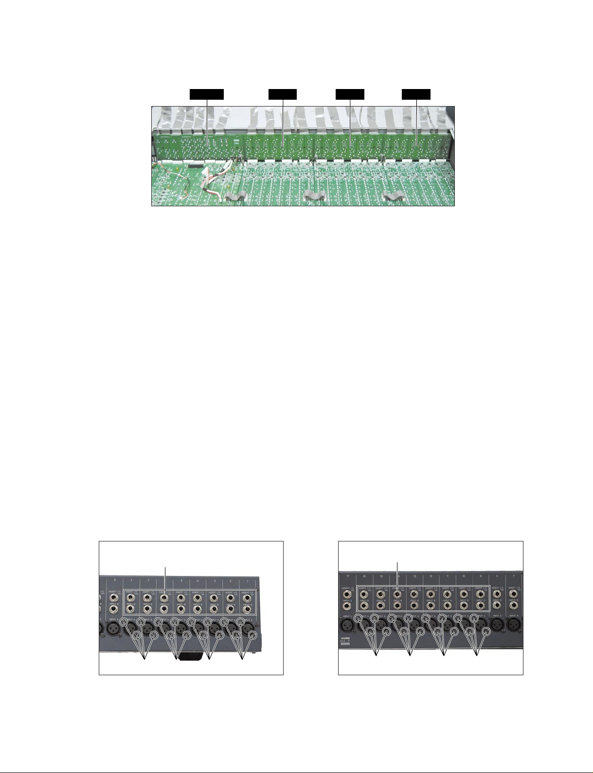
Photo.18(写真18)
MG24/14FX
MG32/14FX
INJK 1INJK 2INJK 3MASJK
11. INJK Circuit Boards 1, 2 and 3
11-1 Remove the bottom cover. (See procedure 2.)
11-2 Set the supports. (See procedure 4.)
11-3 INJK Circuit Board 1:
(Time required: About9 minutes)
11-3-1 Remove the side pad L. (See procedure 1.)
11-3-2 Remove the sixteen (16) screws marked [100A] and
the sixteen (16) hexagonal nuts and flat washer
marked [A]. Then, remove the INJK circuit board 1.
(Photo.18, 19)
11-4 INJK Circuit Board 2:
(Time required: About 9 minutes)
11-4-1 Remove the heat sink. (See procedure 5-3.)
11-4-2 Remove the sixteen (16) screws marked [100B] and
the sixteen (16) hexagonal nuts and flat washer
marked [B]. Then, remove the INJK circuit board 2.
(Photo.18, 20)
11-5 INJK Circuit Board 2:
(Time required: About 10 minutes)
11-5-1 Remove the heat sink. (See procedure 5-3.)
11-5-2 Remove the sixteen (16) screws marked [100C] and
the sixteen (16) hexagonal nuts and flat washer
marked [C]. Then, remove the INJK circuit board 3.
(Photo.18, 21)
11. INJK シート 1、2、3
11-1 ボトムカバーを外します。(2 項参照)
11-2 台を当てます。(4 項参照)
11-3 INJKシート 1:(所要時間:約9分)
11-3-1 サイドパッド L を外します。(1 項参照)
11-3-2 [100A]のネジ16本と[A]の特殊六角ナットと平ワッ
シャ各 16個を外し、INJKシート 1 を外します。
(写真 18、19)
11-4 INJKシート 2:(所要時間:約9分)
11-4-1 [100B]のネジ16本と[B]の特殊六角ナットと平ワッ
シャ各 16個を外し、INJKシート 2 を外します。
(写真 18、20)
11-5 INJKシート 3:(所要時間:約10分)
11-5-1 ヒートシンクを外します。(5-3項参照)
11-5-2 [100C]のネジ16本と[C]の特殊六角ナットと平ワッ
シャ各 16個を外し、INJKシート 3 を外します。
(写真 18、21)
Hexagonalnutandflatwasher[A]
(特殊六角ナットと平ワッシャ[A])
[100]: Bonding Tapping Screw-B
3.0X8 MFZN2BL (VN413300)
Photo.19
(ボンディングBタイト)
(写真19)
Hexagonalnutandflatwasher[B]
(特殊六角ナットと平ワッシャ[B])
[100A][100A][100A][100A]
[100]: Bonding Tapping Screw-B
3.0X8 MFZN2BL (VN413300)
Photo.20
(写真20)
[100B][100B][100B][100B]
(ボンディングBタイト)
41
Page 26
MG24/14FX
MG32/14FX
Hexagonalnutandflatwasher[C]
(特殊六角ナットと平ワッシャ[C])
[100C][100C][100C][100C]
[100]: Bonding Tapping Screw-B
3.0X8 MFZN2BL (VN413300)
Photo.21
12. MASJK Circuit Board
(Time required: About 11 minutes)
12-1 Remove the bottom cover. (See procedure 2.)
12-2 Set the supports. (See procedure 4.)
12-3 Remove the heat sink. (See procedure 5-3.)
12-4 Remove the trans base. (See procedure 6.)
12-5 Remove the DSP shield base. (See procedure 8.)
12-6 Remove the eight (8) screws marked [160] and the
thirty-three (33) hexagonal nuts and flat washer
marked [D]. Then, remove the MASJK circuit board.
(Photo.18, 22)
At the time of DSP shield base attachment,
please tighten the screw of [760] after putting
the pin of the DSP sheet CN101 into CN503 of
MAS 1/4 sheet. (Photo. 14, 28, 39)
(ボンディングBタイト)
(写真21)
12. MASJKシート(所要時間:約 11 分)
12-1 ボトムカバーを外します。(2 項参照)
12-2 台を当てます。(4 項参照)
12-3 ヒートシンクを外します。(5-3 項参照)
12-4 トランスベースを外します。(6 項参照)
12-5 DSPシールドベースを外します。(8 項参照)
12-6 [160]のネジ8本と[D]の特殊六角ナットと平ワッ
シャ各 33個を外し、MASJKシートを外します。
(写真 18、22)
※DSPシールドベース取付時は、DSPシートCN101
のピンをMAS1/4 シートのCN503に入れてから
[760]のネジを締めてください。(写真14、28、29)
42
Hexagonalnut[D]
[160]
[160]
[160]: Bonding Tapping Screw-B 3.0X8 MFZN2BL (VN413300)
2222 (ボンディングBタイト)
Photo.22
(特殊六角ナット[D])
[160]
(写真22)
Page 27
MG24/14FX
MG32/14FX
13. IN Circuit Boards 1, 2 and 3
13-1 Remove the bottom cover. (See procedure 2.)
13-2 Set the supports. (See procedure 4.)
13-3 IN Circuit Board 1:
(Time required: About 9 minutes)
13-3-1 Remove the side pad L. (See procedure 1.)
13-3-2 Remove the eight (8) fader knobs 1. (Photo.23)
13-3-3 Remove the three (3) screws marked [590A].
(Photo.24)
13-3-4 T wist the eighteen (18) hooks of the IN circuit board
1 to become straight. Then, remove the IN circuit
board 1.(Photo.25)
13-4 IN Circuit Board 2:
(Time required: About 9 minutes)
13-4-1 Remove the eight (8) fader knobs 2. (Photo.23)
13-4-2 Remove the three (3) screws marked [590B].
(Photo.24)
13-4-3 T wist the eighteen (18) hooks of the IN circuit board
2 to become straight. Then, remove the IN circuit
board 2.(Photo.25)
13-5 IN Circuit Board 3:
(Time required: About 10 minutes)
13-5-1 Remove the eight (8) fader knobs 3. (Photo.23)
13-5-2 Remove the heat sink. (See procedure 5-3.)
13-5-3 Remove the DSP shield base. (See procedure 8.)
13-5-4 Remove the three (3) screws marked [590C].
(Photo.24)
13-5-5 T wist the eighteen (18) hooks of the IN circuit board
2 to become straight. Then, remove the IN circuit
board 2.(Photo.25)
The push ON buttons, sleeve ON buttons, push
PFL buttons, volume knobs, and push HPF
buttons on the IN circuit boards 1, 2 and 3 are
not components of the circuit board. When you
replace the IN circuit board, you should r emove
the push ON buttons, sleeve ON buttons, push
PFL buttons, volume knobs, and push HPF
buttons from the old IN circuit boards 1, 2 and 3,
and install them in the new circuit board.
(Photo.26)
13. INシート 1、2、3
13-1 ボトムカバーを外します。(2 項参照)
13-2 台を当てます。(4 項参照)
13-3 INシート 1:(所要時間:約9 分)
13-3-1 サイドパッド L を外します。(1 項参照)
13-3-2 ノブ(FADER1)8 個を外します。(写真23)
13-3-3 [590A]のネジ 3 本を外します。(写真 24)
13-3-4 IN シート1を固定しているフック18箇所をまっす
ぐになるようにひねり、IN シート1を外します。
(写真 25)
13-4 INシート 2:(所要時間:約9 分)
13-4-1 ノブ(FADER2)8 個を外します。(写真23)
13-4-2 [590B]のネジ 3 本を外します。(写真 24)
13-4-3 IN シート2を固定しているフック18箇所をまっす
ぐになるようにひねり、IN シート2を外します。
(写真 25)
13-5 INシート 3:(所要時間:約10 分)
13-5-1 ノブ(FADER3)8 個を外します。(写真23)
13-5-2 ヒートシンクを外します。(5-3項参照)
13-5-3 DSP シールドベースを外します。(8 項参照)
13-5-4 [590C]のネジ 3 本を外します。(写真 24)
13-5-5 IN シート3を固定しているフック18箇所をまっす
ぐになるようにひねり、IN シート3を外します。
(写真 25)
※ IN シート 1、2、 3上のボタンONAss y、 スリーブ
ONボタン、ボタンPFL、ノブ(VR)、ボタンHPFは、
INシート1、2、3の構成部品ではありません。INシー
トを交換する際には、INシート1、2、3からボタン
ONAssy、スリーブONボタン、ボタンPFL、ノブ
(VR)、ボタンHPFを取り外して、新しいINシート
1、2、3 に取り付けてください。(写真 26)
Faderknob1x8
(ノブ(FADER1))
Faderknob2x8
(ノブ(FADER2))
Photo.23(写真23)
Faderknob3x8
(ノブ(FADER3))
43
Page 28

MG24/14FX
)
MG32/14FX
[590C]
[590]: Bind Head Tapping Screw-S
3.0X6 MFZN2BL (EP630210)
Photo.24
(写真24)
IN 1IN 2IN 3
[590A][590B]
(+バインドSタイト)
Hooks
(フック)
PushHPFbuttons
(ボタンHPF)
IN 2IN 3
Hooks(フック)
IN 1
Hooks(フック
Photo.25(写真25)
PushHPFbuttons
(ボタンHPF)
PushPFLbuttons
(ボタンPFL)
PushONbuttons
(ボタンONAss'y)
SleeveONbuttons
(スリーブONボタン)
Volumeknob
(ノブ(VR))
Photo.26(写真26)
14. MAS 1/4 to 4/4 Circuit Boards
(Time required: About 15 minutes)
14-1 Remove the bottom cover. (See procedure 1.)
14-2 Set the supports. (See procedure 4.)
14-3 Remove the heat sink. (See procedure 5-3.)
14-4 Remove the DSP shield base. (See procedure 8.)
14-5 MAS 2/4: (Time required: About 7 minutes)
14-5-1 Remove the two (2) screws marked [390A] from the
control panel surface. Then, remove the MAS 2/4
circuit board. (Photo.27, 30)
14-6 MAS 3/4: (Time required: About 7 minutes)
14-6-1 Remove the two (2) screws marked [390B] from the
control panel surface. Then, remove the MAS 3/4
circuit board. (Photo.27, 30)
14-7 MAS 4/4: (Time required: About 7 minutes)
14-7-1 Remove the hexagonal nut and flat washer [E] from
the control panel surface.Then, remov e the MAS 4/4
circuit board. (Photo.27, 30, 31)
14. MAS1/4 〜 4/4 シート
14-1 ボトムカバーを外します。(1 項参照)
14-2 台を当てます。(4 項参照)
14-3 ヒートシンクを外します。(5-3 項参照)
14-4 DSPシールドベースを外します。(8 項参照)
14-5 MAS2/4:(所要時間:約 7分)
14-5-1 コントロールパネル面から、[390A]のネジ2本を外
して、MAS2/4シートを外します。(写真 27、30)
14-6 MAS3/4:(所要時間:約 7分)
14-6-1 コントロールパネル面から、[390B]のネジ2本を外
し、MAS3/4シートを外します。(写真 27、30)
14-7 MAS4/4:(所要時間:約 7分)
14-7-1 [E]の特殊六角ナットと平ワッシャ1個を外し、MAS
4/4 シートと基板固定金具を外します。
(写真27、30、31)
44
Page 29

MG24/14FX
MG32/14FX
14-8 MAS 1/4: (Time required: About 12 minutes)
14-8-1 Remove the side pad R. (See procedure 1.)
14-8-2 Remove the twelve (12) fader knobs and the tw o (2)
select knobs from the control panel surface.
(Photo.27)
14-8-3 Remove the MAS 2/4 circuit board.
(See procedure 14-5.)
14-8-4 Remove the MAS 3/4 circuit board.
(See procedure 14-6.)
14-8-5 Remove the MAS 4/4 circuit board.
(See procedure 14-7.)
14-8-6 Remove the f our (4) screws marked [380]. (Photo .29)
14-8-7 Twist the twenty-four (24) hooks of the MAS 1/4
circuit board to become straight. Then, remove the
MAS 1/4, 3/4, and 4/4 circuit boards. (Photo.30)
The meter reflector, push ON buttons, sleeve ON
buttons, push PFL buttons, holder circuit board,
volume knobs, push HPF buttons, push TAP
buttons, and meter cover, push spacer on the
MAS 1/4 circuit board are not components of
the circuit board. When you replace the MAS 1/
4 circuit board, you should remove the meter
reflector, push ON buttons, sleeve ON buttons,
push PFL buttons, holder circuit board, volume
knobs, push HPF buttons, push T AP buttons, and
meter cover, push spacer from the old MAS 1/4
circuit board, and install in the new circuit boar d.
(Photo. 31)
At the time of DSP shield base attachment,
please tighten the screw of [760] after putting
the pin of the DSP sheet CN101 into CN503 of
MAS 1/4 sheet. (Photo. 14, 28, 29)
14-8 MAS1/4:(所要時間:約 12分)
14-8-1 サイドパッド R を外します。(1 項参照)
14-8-2 コントロールパネル面から、ノブ(FADER)12個と
ノブ(SELECT)2 個を外します。(写真 27)
14-8-3 MAS2/4 シートを外します。(14-5 項参照)
14-8-4 MAS3/4 シートを外します。(14-6 項参照)
14-8-5 MAS4/4 シートを外します。(14-7 項参照)
14-8-6 [380]のネジ 4 本を外します。(写真 29)
14-8-7 MAS1/4 シートを固定しているフック24 箇所を
まっすぐになるようにひねり、MAS1/4 シートを
外します。(写真 30)
※MAS1/4シート上のリフレクターMETER、ボタン
ONAssy、スリーブ ONボタン、ボタンPFL、基
板固定金具、ノブ(VR)、ボタンHPF、ボタンTAP、
ウインドウMETER、プッシュスペーサーは、MAS
1/4 シートの構成部品ではありません。MA S 1 / 4
シートを交換する際には、MAS1/4 シートからリ
フレクターMETER、ボタンONAssy、スリーブ
ONボタン、ボタンPFL、基板固定金具、ノブ(VR)、
ボタンHPF、ボタンTAP、ウインドウMETER、プッ
シュスペーサーを取り外して、新しいMAS1/4シー
トに取り付けてください。(写真 31)
※DSPシールドベース取付時は、DSPシートCN101
のピンを MAS1/4 シートのCN503に入れてから
[760]のネジを締めてください。(写真14、28、29)
[390]: Bonding Tapping Screw-B 3.0X8 MFZN2BL (VN413300)(ボンディングBタイト)
Photo.27
Hexagonalnut
andflatwasher[E]
(特殊六角ナットと
平ワッシャ[E])
Faderknob
(ノブ(FADER))
(写真27)
Selectknob
(ノブ(SELECT))
[390A]
[390B]
45
Page 30

MG24/14FX
MG32/14FX
DSP:CN101
DSPshieldbase
(DSPシールドベース)
Photo.28 (写真28)
[380]
MAS 1/4
Hooks x24
(フック)
MAS1/4:CN503
Photo.29 (写真29)
MAS 2/4MAS 3/4MAS 4/4MAS 1/4
46
PushONbuttons
(ボタンONAss'y)
PushPFLbuttons
(ボタンPFL)
PushHPFbuttons
(ボタンHPF)
Volumeknob
PushTAPbuttons
(ボタンTAP)
(ノブ(VR))
Photo.30 (写真30)
MAS 1/4
Photo.31 (写真31)
Metercover
(ウインドウMETER)
MAS 3/4
TootheLockWasher
(歯付座金)
Holder,circuitboard
MAS 4/4
(基板固定金具)
Meterreflector
(リフレクターMETER)
Page 31
MIXING CONSOLE
CIRCUIT DIAGRAM
CONTENTS
BLOCK DIAGRAM
(ブロックダイアグラム&レベルダイアグラム)
OVERALL CIRCUIT DIAGRAM
DSP .................................................................................. 4
IN ..................................................................................5-9
INJK............................................................................... 10
MAS 1/4....................................................................11-18
MAS 2/4.........................................................................18
MAS 3/4.........................................................................14
MAS 4/4.........................................................................18
MASJK ....................................................................19, 20
PS................................................................................... 21
Notation for Circuit Diagrams
1. How to identify inter-sheet connectors
ONLED
Signal name
(信号名)
(目次)
&LEVELDIAGRAM
(総回路図)
(回路図表記上の注意)
(シート間コネクタの読み方について)
to page 8: N7
The page number indicates the destination page.
(ページNo.は信号の行先ページを示します。)
This indicates the location of the counter inter-sheet connector.
(The alphabet indicates horizontal direction and the number
indicates vertical direction)
対応するシート間のコネクタのあるロケーションを示します。
(アルファベットが水平方向、数字が垂直方向)
.................... 3
Note: See parts list for details of circuit board component parts.
注:シートの部品詳細はパーツリストをご参照ください。
Page 32
ABCDEFGH
BLOCK DIAGRAM & LEVEL DIAGRAM
INJK
JK101, 201, 301, 401, 501,
CH INPUT
ST CH INPUT
ST CH INPUT
[-34dBu to +10dBu]
601, 701, 801
[-60dBu to -16dBu]
[-34dBu to +10dBu]
MG24/14FX: CH1-16
MG32/14FX: CH1-24
JK102, 202, 302, 402, 502,
602, 702, 802
[-34dBu to +10dBu]
MG24/14FX: CH17(L)/18(R), CH19(L)/20(R)
MG32/14FX: CH25(L)/26(R), CH27(L)/28(R)
MG24/14FX: CH21(L)/22(R), CH23(L)/24(R)
MG32/14FX: CH29(L)/30(R), CH31(L)/32(R)
A
B
JK106, 108, 109
MASJK
JK102, 104
JK105, 107, 109
MG24/14FX: [CH1-8] [CH9-16]
MG32/14FX: [CH1-8] [CH9-16] [CH17-24]
PHANTOM
BCH/SW
IC101, 102, 201, 301, 302, 401, 501,
502, 601, 701, 702, 801 (8P)
GAIN
[-60dBu~-16dBu]
[-34dBu~+10dBu]
INSERT I/O
[0dBu]
MG24/14FX: CH1-16
MG32/14FX: CH1-24
JK101, 103
L
R
CN101 (13P) CN101 (13P)
IC101a, 201a (8P)
IC101b, 201b (8P)
MAS 1/4
1
L
R
Same As 1
CN101, 102,103, 104 (13P)
GAIN
[-34dBu~+10dBu]
IC103, 104, 203, 303,
304, 403, 503,
504, 603, 703,
704, 803 (8P)
JK103, 203, 303,
403, 503, 603,
703, 803
CN105 (3P)
IC102b, 103b, 104b, 105 (8P)
202b, 203b, 204b (8P)
IC102a, 103a, 104a,
202a, 203a, 204a,
205 (8P)
IC301, 401 (8P)
MAS 3/4
CH Fader
IC105a, 205a, 305a,
405a, 505a, 605a,
CN101,
705a, 805a (8P)
102,
103,
104
(13P)
CN105 (3P)
IC302, 303, 304, 305,
402, 403, 404 (8P)
RETURN 1, 2
[+4dBu]
CN101 (34P)
CN503 (34P)
DSP
TAP
JK701
CN701
(3P)
FOOT
SWITCH
MASJK
IN
IC105b, 205b, 305b,
405b, 505b, 605b,
705b, 805b (8P)
IC106b, 206b (8P)
ST CH fader
IC106a,
206a (8P)
IC107b,
207b (8P)
IC306, 307, 406, 407 (8P)
JK201, 203
L (MONO)
JK202, 204
2TR IN
[-10dBu]
JK901
MIC
[-50dBu]
CN901 (3P)
CN502 (3P)
R
CN201
(13P)
JK205
IC902a (8P)
CN902 (3P)
Same As 2
2
IC107a, 207a (8P)
CN501
(13P)
IC901a (8P)
L
R
IC901b (8P)
CN106, 109,111
IC501a, 502a (8P)
IC501b,
502b
(8P)
IC902b (8P)
IC503 (8P)
IC504a (8P)
IC504b (8P)
CN903, 301, 302
IC701, 702,
707 (8P)
G. INSERT I/O
[0dBu]
JK401-404
IC801a
(8P)
IC801b
(8P)
IC903a (8P)
IC904a
(8P)
IC905b (8P)
IC905a (8P)
IC601, 602,
603 (8P)
IC604b (8P)
IC604a (8P)
CN401
(13P)
ST INSERT I/O
[0dBu]
L
JK505
R
MASJK
JK506
REC OUT
[-10dBu]
JK205
IC806 (8P)
IC903b (8P)
IC904b
(8P)
IC605, 606,
607 (8P)
CN601 (13P)
IC608b (8P)
IC608a (8P)
GROUP Fader
IC705, 706 (8P)
CN701 (13P)
IC703, 704 (8P)
CN702 (13P)
IC807b (8P)
IC906a (8P)
IC906b (8P)
CN301 (13P)
GROUP OUT 1-4
CN501 (13P)
IC802a
(8P)
ST Fader
IC802b
(8P)
IC805b (8P)
ST SUB
IC805a (8P)
MONO Fader
IC807a (8P)
IC908b (8P)
PHONES
IC908a (8P)
CN906 (3P)
AUX OUT 1~6
[+4dBu]
JK301~306
EFFECT OUT 1
[+4dBu]
JK307
EFFECT OUT 2
[+4dBu]
JK308
[+4dBu]
JK501, 502,
503, 504
IC803
(8P)
IC804
(8P)
CN801
(13P)
IC808
(8P)
CN907 (3P)
ST OUT
[+4dBu]
JK601
JK602
MASJK
CN601
(13P)
ST SUB OUT
[+4dBu]
JK604
JK605
JK603
MONO OUT
[+4dBu]
MASJK
JK902
PHONES
[3mW @ 40ohms ]
MASJK
IC909 (24P)
IC910
(24P)
IC911
(24P)
IC912 (24P)
MAS
4/4
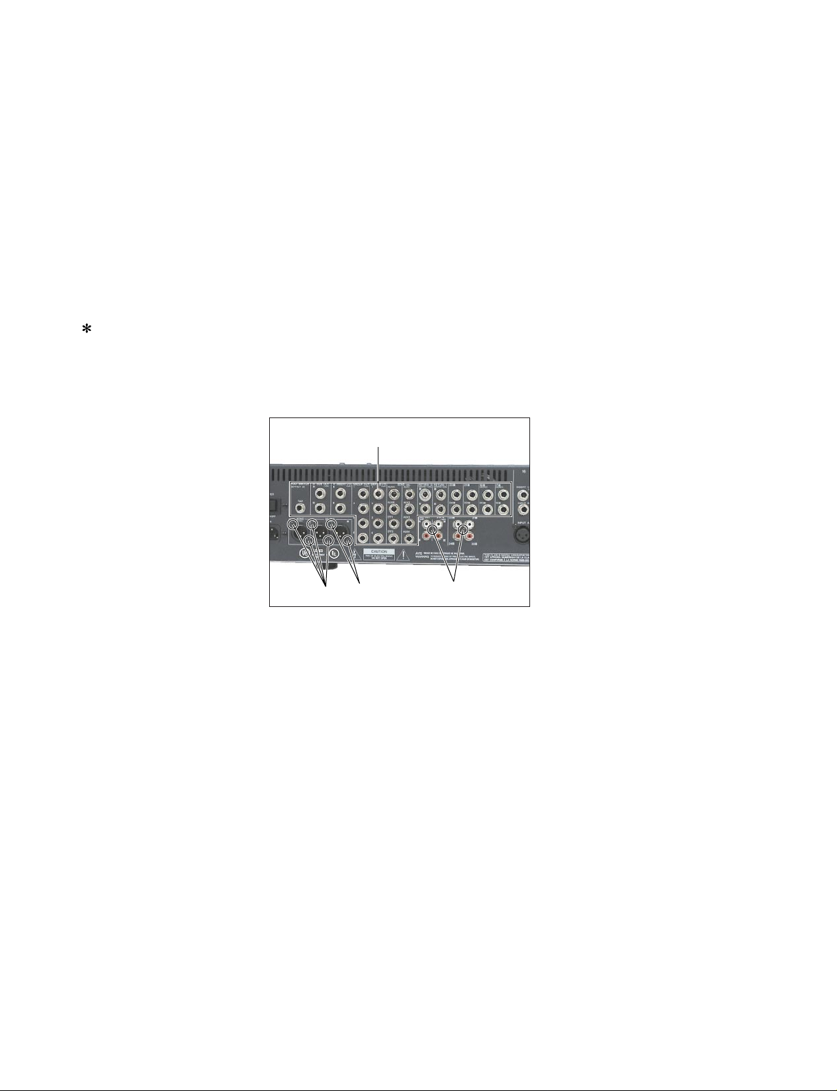
This is a diagram about ST OUT and MONO OUT when a signal inputs from
one of the ST INSERT L INPUT and the ST INSERT R INPUT.
ST INSERT I/O
[0dBu]
L
JK505
R
JK506
MASJK
CN501 (13P)
IC802a
(8P)
ST Fader
IC802b
(8P)
IC805, 806
(8P)
CN702
(13P)
IC803
(8P)
IC804
(8P)
MAS 1/4
ST OUT
L
[+4dBu]
JK601
R
JK602
IC807
(8P)
CN801 (13P)
MASJK
CN601 (13P)
IC808
(8P)
MONO
OUT
JK603
MG24/14FX
MG32/14FX
1
2
3
4
38CA1-8828050
5
1
3
6
Page 33

ABCDEFGHIJKLMNOPQRSTUVWXY
1
OVERALL CIRCUIT DIAGRAM 1/18 (DSP)
DSP
REGULATOR +3.3V
SYSTEM RESET
MG24/14FX
MG32/14FX
2
3
MCU EEPROM 2K
4
5
6
7
to MAS 1/4-CN503
(to Page 15)
DIR2
N.C
AND
N.C
8
9
10
11
12
13
14
µPC29M33T-E1(XU965A00)
REGULATOR +3.3V
2
1
3
1: INPUT
2: COMMON
3: OUTPUT
OP AMP
OP AMP
OP AMP
OP AMP
AND
INVERTER
DRAM 4M
CODEC
DSP6
CODEC
15
16
17
OP AMP
OP AMP
*
Note: R113 R163 R164 R364 is not necessary to mount.
28CC1-8828049
4
2
: Mylar Capacitor
: Ceramic Capacitor
(
セラミックコンデンサー
(
マイラーコンデンサー
)
)
DRAM 4M
Page 34
ABCDEFGHIJKLMNOPQR
OVERALL CIRCUIT DIAGRAM 2/18 (IN)
to INJK-CN105
(to Page 10)
to INJK-CN101
(to Page 10)
IN
to Page 7: F12
OP AMP
OP AMP
OP AMP
OP AMP
OP AMP
OP AMP
OP AMP
OP AMP
OP AMP
MG24/14FX
MG32/14FX
1
2
3
4
5
to MAS 1/4-CN903
(to Page 18)
to IN-CN107
to INJK-CN102
(to Page 10)
to IN-CN106
to Page 7: F12
to Page 8: O11
OP AMP
OP AMP
OP AMP
OP AMP
OP AMP
OP AMP
OP AMP
OP AMP
OP AMP
OP AMP
OP AMP
OP AMP
6
7
8
9
10
28CC1-8828045-1
11
OP AMP
OP AMP
to Page 8: J11
2
: Ceramic Capacitor
: Mylar Capacitor
: Metal Film Resistor (chip)
(
セラミックコンデンサー
(
マイラーコンデンサー
(チップ
金属被膜抵抗
)
)
)(D)
OP AMP
12
5
1
Page 35
ABCDEFGHIJKLMNOPQR
OVERALL CIRCUIT DIAGRAM 3/18 (IN)
1
IN
OP AMP
OP AMP
MG24/14FX
MG32/14FX
2
OP AMP
3
to INJK-CN103
(to Page 10)
to Page 8: E11
OP AMP
OP AMP
4
OP AMP
OP AMP
OP AMP
5
OP AMP
6
7
8
9
10
to INJK-CN104
(to Page 10)
to Page 9: O11
to Page 9: J11
OP AMP
OP AMP
OP AMP
OP AMP
OP AMP
OP AMP
OP AMP
OP AMP
OP AMP
OP AMP
OP AMP
11
12
13
OP AMP
OP AMP
OP AMP
to Page 9: E11
: Ceramic Capacitor
28CC1-8828045-2
6
2
: Mylar Capacitor
: Metal Film Resistor (chip)
(
セラミックコンデンサー
(
マイラーコンデンサー
(チップ
金属被膜抵抗
)
)
OP AMP
)(D)
Page 36

ABCDEFGHIJKLMNOPQR
OVERALL CIRCUIT DIAGRAM 4/18 (IN)
to MAS 1/4-CN301
to IN-CN108
to IN-CN109 to IN-CN111
to MAS 1/4-CN302
to IN-CN110
IN
MG24/14FX
MG32/14FX
to Page 8: P1, 9: P1
to Page 8: P2, 9: P2
1
2
3
4
5
: Ceramic Capacitor
(
セラミックコンデンサー
6
7
to Page 8: N7
OP AMP
OP AMP
8
9
to Page 8: N8
10
)
OP AMP
OP AMP
11
28CC1-8828045-3
12
2
to Page 5: N4 to Page 5: N7
7
Page 37
ABCDEFGHIJKLMNOPQ
OVERALL CIRCUIT DIAGRAM 5/18 (IN)
1
IN
2
from Page 7: B1, 8: A1
from Page 7
from Page 7
from Page 7
MG24/14FX
MG32/14FX
to Page 9: P1
to Page 9: P2
3
4
5
6
7
8
9
10
OP AMP
from Page 7: D8
from Page 7: D10
OP AMP
OP AMP
OP AMP
to Page 9: N7
OP AMP
to Page 9: N8
OP AMP
11
12
28CC1-8828045-4
to Page 5: N10
2
to Page 5: N12
from Page 6: N4
8
Page 38

ABCDEFGHIJKLMNOPQ
IN
from Page 7: B2, 8: A1
from Page 7: B2, 8: A2
from Page 7: B3, 8: A2
OVERALL CIRCUIT DIAGRAM 6/18 (IN)
from Page 7: B1, 8: A1
MG24/14FX
MG32/14FX
1
2
3
4
5
OP AMP
from Page 8: B7
from Page 8: B9
OP AMP
OP AMP
OP AMP
6
7
OP AMP
8
9
10
OP AMP
28CC1-8828045-5
from Page 6: N6
2
from Page 6: N9
from Page 6: N12
11
12
9
Page 39

ABCDEFGHIJKL
OVERALL CIRCUIT DIAGRAM 7/18 (INJK)
1
MG24/14FX
MG32/14FX
INJK
to IN-CN105
(to Page 5)
2
INPUT A
MG24/14FX: CH1, 9
MG32/14FX: CH1, 9, 17
INPUT A
MG24/14FX: CH3, 11
MG32/14FX: CH3, 11, 19
INPUT A
MG24/14FX: CH5, 13
MG32/14FX: CH5, 13, 21
INPUT A
MG24/14FX: CH7, 15
MG32/14FX: CH7, 15, 23
3
INPUT B
MG24/14FX: CH1, 9
MG32/14FX: CH1, 9, 17
4
INSERT I/O 0dBu
MG24/14FX: CH1, 9
MG32/14FX: CH1, 9, 17
INPUT B
MG24/14FX: CH3, 11
MG32/14FX: CH3, 11, 19
INSERT I/O 0dBu
MG24/14FX: CH3, 11
MG32/14FX: CH3, 11, 19
INPUT B
MG24/14FX: CH5, 13
MG32/14FX: CH5, 13, 21
INSERT I/O 0dBu
MG24/14FX: CH5, 13
MG32/14FX: CH5, 13, 21
INPUT B
MG24/14FX: CH7, 15
MG32/14FX: CH7, 15, 23
INSERT I/O 0dBu
MG24/14FX: CH7, 15
MG32/14FX: CH7, 15, 23
to IN-CN101 (to Page 5)
5
6
INPUT A
MG24/14FX: CH2, 10
MG32/14FX: CH2, 10, 18
INPUT B
MG24/14FX: CH2, 10
MG32/14FX: CH2, 10, 18
INSERT I/O 0dBu
MG24/14FX: CH2, 10
MG32/14FX: CH2, 10, 18
INPUT A
MG24/14FX: CH4, 12
MG32/14FX: CH4, 13, 20
INPUT B
MG24/14FX: CH4, 12
MG32/14FX: CH4, 12, 20
INSERT I/O 0dBu
MG24/14FX: CH4, 12
MG32/14FX: CH4, 12, 20
to IN-CN102 (to Page 5)
INPUT A
MG24/14FX: CH6, 14
MG32/14FX: CH6, 14, 22
INPUT B
MG24/14FX: CH6, 14
MG32/14FX: CH6, 14, 22
INSERT I/O 0dBu
MG24/14FX: CH6, 14
MG32/14FX: CH6, 14, 22
to IN-CN103 (to Page 6)
INPUT A
MG24/14FX: CH8, 16
MG32/14FX: CH8, 16, 24
INPUT B
MG24/14FX: CH8, 16
MG32/14FX: CH8, 16, 24
INSERT I/O 0dBu
MG24/14FX: CH8, 16
MG32/14FX: CH8, 16, 24
to IN-CN104
(to Page 6)
7
: not installed
: Metal Film Resistor
8
(LL)
: Low Leakage Current Electrolytic Capacitor
(未実装)XX
(
金属被膜抵抗
)(F)
(低漏れ電流電解コンデンサー)
10
28CC1-8828047
1
Page 40
ABCDEFGHIJKLMNOPQ
OVERALL CIRCUIT DIAGRAM 8/11 (MAS 1/4)
MAS 1/4
to Page 12: L12 to Page 12: K12 to Page 12: F12 to Page 12: E12 to Page 13: M12 to Page 13: L12 to Page 13: G12 to Page 13: F12
OP AMP
OP AMP
OP AMP
OP AMP
OP AMP
OP AMP
OP AMP
OP AMP
OP AMP
OP AMP
OP AMP
OP AMP
OP AMP
OP AMP
OP AMP
OP AMP
MG24/14FX
MG32/14FX
1
2
3
4
5
OP AMP
OP AMP
OP AMP
OP AMP
OP AMP
OP AMP
OP AMP
OP AMP
OP AMP
OP AMP
OP AMP
OP AMP
OP AMP
OP AMP
OP AMP
OP AMP
OP AMP
OP AMP
6
OP AMP
7
8
9
10
OP AMP
28CC1-8828044-1
11
: Ceramic Capacitor
2
to MASJK-CN101
(to Page 19)
: Mylar Capacitor
(
セラミックコンデンサー
(
マイラーコンデンサー
)
)
12
11
Page 41

ABCDEFGHIJKLMNOPQ
OVERALL CIRCUIT DIAGRAM 9/18 (MAS 1/4)
1
MAS 1/4
2
MG24/14FX
MG32/14FX
to Page 13: O1, 14: P2, 18: P11
to Page 13: O1, 14: P2, 18: P10
to Page 13: O1, 14: P3, 18: P9
to Page 13: O1, 16: C11
to Page 13: O1, 16: E11
to Page 13: O2, 16: G11
to Page 13: O2, 16: H11
to Page 13: O2, 14: P3, 16: J11
to Page 13: O2, 14: P3, 16: K11
to Page 13: O2, 14: P3, 16: M11
to Page 13: O2, 14: P3, 16: O11
to Page 13: O2, 17: P12
to Page 13: O2, 17: L12
to Page 13: O2, 17: N12
to Page 13: O2, 17: P12
to Page 13: O3, 14: P3, 17: P11
to Page 13: O3, 14: P3, 17: P11
3
to IN-CN108, 109
(to Page 7)
to IN-CN110, 111
(to Page 7)
4
5
OP AMP OP AMP
6
7
8
9
10
: Ceramic Capacitor
(
セラミックコンデンサー
)
OP AMP
OP AMP
OP AMP
OP AMP
OP AMP
OP AMP
11
12
12
28CC1-8828044-2
to Page 13: N11
to Page 13: N11
2
from Page 11: P3 from Page 11: N3
from Page 11: L3 from Page 11: K3
Page 42

ABCDEFGHIJKLMNOPQ
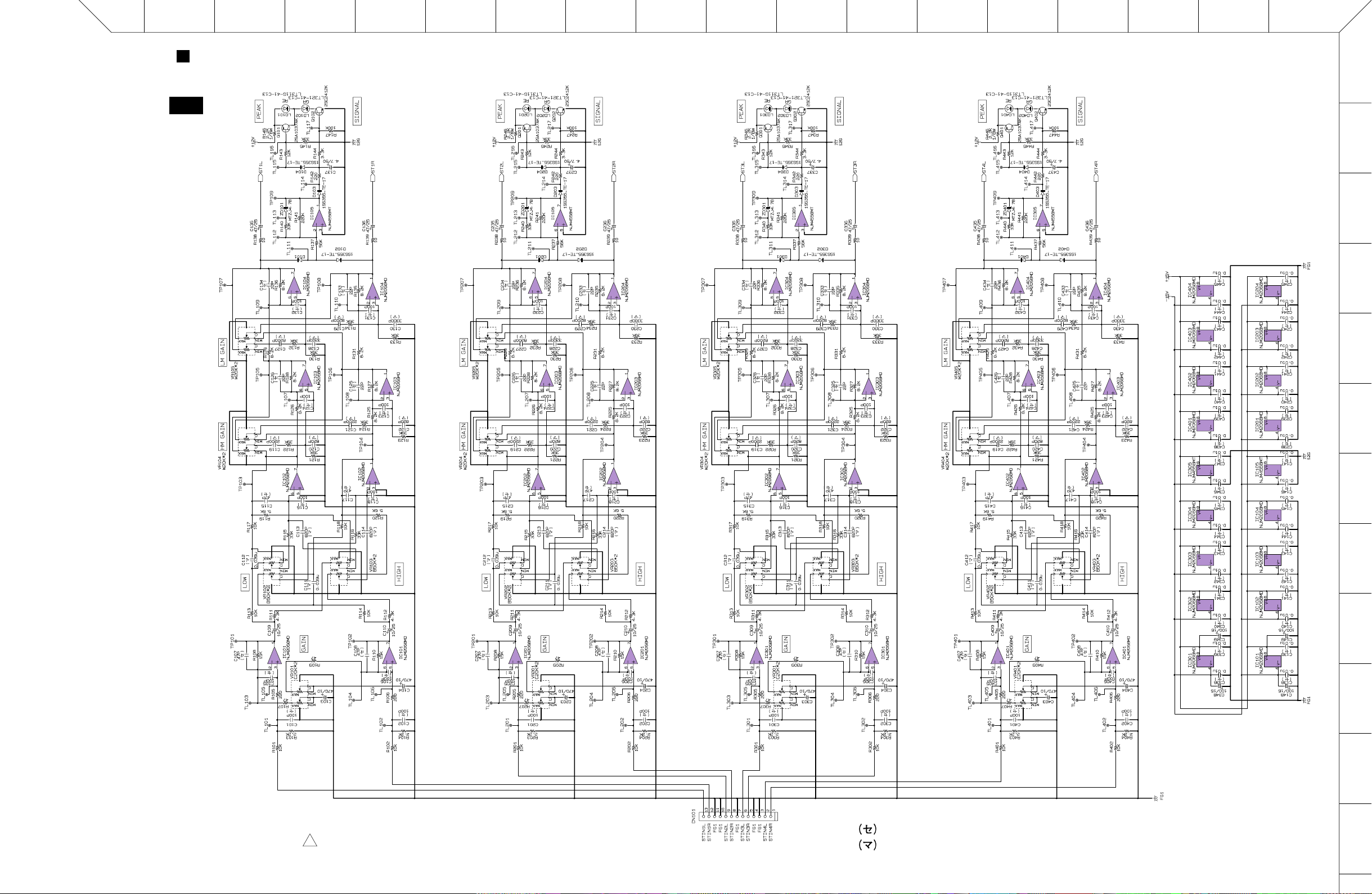
OVERALL CIRCUIT DIAGRAM 10/18 (MAS 1/4)
from Page 12: A1, 14: B2, 15: A1
from Page 12: A1, 14: B2, 15: A1
from Page 12: A1, 14: B3, 15: A1
from Page 12: A1
from Page 12: A1
from Page 12: A2
from Page 12: A2
from Page 12: A2, 14: B3, 15: B1
from Page 12: A2, 14: B3, 15: B1
from Page 12: A2, 14: B3, 15: B1
from Page 12: A2, 14: B3, 15: B1
from Page 12: A2, 15: B1
from Page 12: A2, 15: B1
from Page 12: A2, 15: B1
from Page 12: A2, 15: B1
from Page 12: A3, 14: B3, 15: B1
from Page 12: A3, 14: B3, 15: B1
MAS 1/4
OP AMP
OP AMP
MG24/14FX
MG32/14FX
to Page 14: P2, 18: P11
to Page 14: P2, 18: P10
to Page 14: P3, 18: P9
to Page 16: C11
to Page 16: E11
to Page 16: G11
to Page 16: H11
to Page 14: P3, 16: J11
to Page 14: P3, 16: K11
to Page 14: P3, 16: M11
to Page 14: P3, 16: O11
to Page 17: P12
to Page 17: L12
to Page 17: N12
to Page 17: P12
to Page 14: P3, 17: P11
to Page 14: P3, 17: P11
1
2
3
4
5
OP AMP
OP AMP
OP AMP
OP AMP
6
OP AMP
7
OP AMP
8
9
10
28CC1-8828044-3
from Page 12: B11
from Page 12: B11
2
from Page 11: I3 from Page 11: G3 from Page 11: E3 from Page 11: D3
: Ceramic Capacitor
(
セラミックコンデンサー
)
13
11
12
Page 43
ABCDEFGHIJKLMNOPQ
1
2
from Page 12: A1, 13: A1, 15: A1
from Page 12: A1, 13: A1, 15: A1
from Page 12: A1, 13: A1, 15: A1
from Page 12: A2, 13: A2, 15: B1
from Page 12: A2, 13: A2, 15: B1
from Page 12: A2, 13: A2, 15: B1
from Page 12: A2, 13: A2, 15: B1
3
from Page 12: A3, 13: A2, 15: B1
from Page 12: A3, 13: A3, 15: B1
4
5
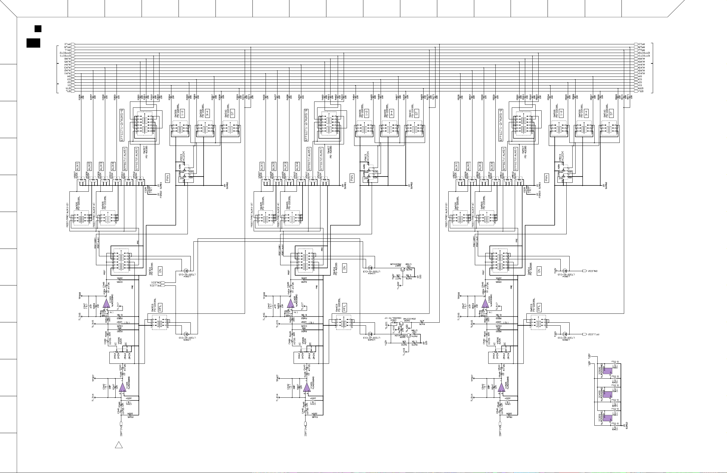
OVERALL CIRCUIT DIAGRAM 11/18 (MAS 1/4, MAS 3/4)
MAS 1/4
MG24/14FX
MG32/14FX
to Page 13: O1, 18: P11
to Page 13: O1, 18: P10
to Page 13: O1, 18: P9
to Page 13: O2, 16: J11
to Page 13: O2, 16: K11
to Page 13: O2, 16: M11
to Page 13: O2, 16: O11
to Page 13: O3, 17: P11
to Page 13: O3, 17: P11
6
7
8
9
10
OP AMP
OP AMP
OP AMP
OP AMP
to MASJK-CN201
(to Page 19)
OP AMP
OP AMP
OP AMP
OP AMP
MAS 3/4
MIC
-50dBu
11
12
14
28CC1-8828044-4
: Ceramic Capacitor
(
セラミックコンデンサー
)
2
Page 44

ABCDEFGHIJKLMNOPQ
STL
OVERALL CIRCUIT DIAGRAM 12/18 (MAS 1/4)
MAS 1/4
to MASJK-CN701 (to Page 20)
to DSP-CN101
(to Page 4)
from Page 16: E2
from Page 16: D2
OP AMP
to Page 13: O3, 14: P3, 17: P11
STR
to Page 13: O3, 14: P3, 17: P11
G1
to Page 13: O2, 17: P12
G2
to Page 13: O2, 17: N12
G3
to Page 13: O2, 17: L12
G4
to Page 13: O2, 17: P12
MG24/14FX
MG32/14FX
AUX1
to Page 13: O2, 14: P3, 16: O11
AUX2
to Page 13: O2, 14: P3, 16: M11
AUX3
to Page 13: O2, 14: P3, 16: K11
AUX4
to Page 13: O2, 14: P3, 16: J11
PFLL
to Page 13: O1, 14: P3, 18: P9
PFLR
to Page 13: O1, 14: P2, 18: P10
PFLCTL
to Page 13: O1, 14: P2, 18: P11
1
2
3
OP AMP
4
OP AMP
OP AMP
5
6
7
8
9
28CC1-8828044-5
: Ceramic Capacitor
2
(
セラミックコンデンサー
10
)
11
15
12
Page 45

BCDEFGHIJKLMNOPQ
1
OVERALL CIRCUIT DIAGRAM 13/18 (MAS 1/4)
to MASJK-CN301
(to Page 19)
to Page 15: N3 to Page 15: N3
MG24/14FX
MG32/14FX
A
MAS 1/4
2
3
OP AMP OP AMP OP AMP OP AMP OP AMP OP AMP OP AMP OP AMP
4
5
6
7
OP AMP
8
OP AMP
OP AMP
OP AMP OP AMP
OP AMP OP AMP
OP AMP
OP AMP
9
10
11
12
16
OP AMP
28CC1-8828044-6
from Page 12: A2, 13: A2,
14: B3, 15: B1
2
from Page 12: A2, 13: A2,
14: B3, 15: B1
from Page 12: A2, 13: A2,
14: B3, 15: B1
from Page 12: A2, 13: A2,
14: B3, 15: B1
from Page 12: A2, 13: A2
: Ceramic Capacitor
from Page 12: A2, 13: A2
(
セラミックコンデンサー
to Page 17: P11, 18: P7
to Page 17: P11, 18: P8
from Page 12: A1, 13: A1 from Page 12: A1, 13: A1
)
Page 46

ABCDEFGHIJKLMNOPQR
OVERALL CIRCUIT DIAGRAM 14/18 (MAS 1/4)
to MASJK-CN501
(to Page 20)
to MASJK-CN401 (to Page 20)
MAS 1/4
OP AMP
OP AMP
to Page 18: N4
OP AMP
OP AMP
OP AMP
to Page 18: N4
OP AMP
to Page 18: N5
OP AMP
OP AMP
OP AMP
to Page 18: N5
to Page 18: N4
to Page 18: N4
OP AMP
OP AMP
OP AMP
OP AMP
OP AMP
OP AMP
to MASJK-CN601
(to Page 20)
OP AMP
OP AMP
MG24/14FX
MG32/14FX
OP AMP
1
2
3
OP AMP
4
5
6
OP AMP
from Page 16: B10
from Page 12: A3, 13: A2, 14: B3, 15: B1
from Page 12: A3, 13: A3, 14: B3, 15: B1
from Page 16: B10
OP AMP
OP AMP
OP AMP
OP AMP
OP AMP
OP AMP
OP AMP
OP AMP
OP AMP
OP AMP
7
8
9
10
11
from Page 12: A2, 13: A2, 15: B1
28CC1-8828044-7
from Page 12: A2, 13: A2, 15: B1 from Page 12: A2, 13: A2, 15: B1 from Page 12: A2, 13: A2, 15: B1
2
: Ceramic Capacitor
: Mylar Capacitor
: Metal Film Resistor (chip)
(
セラミックコンデンサー
(
マイラーコンデンサー
(チップ
金属被膜抵抗
)
)
)(D)
17
13
12
Page 47
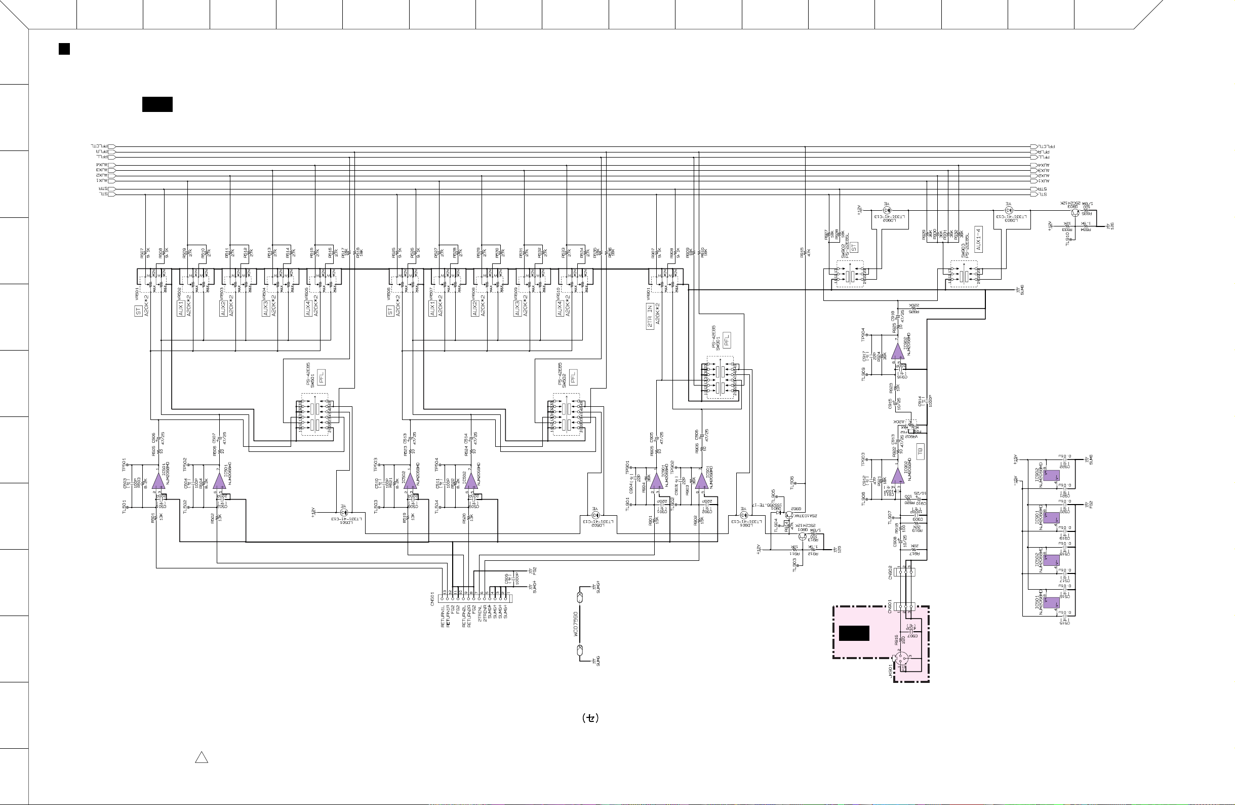
ABCDEFGHIJKLMNOPQR
OVERALL CIRCUIT DIAGRAM 15/18 (MAS 1/4, 2/4, 4/4)
to PS-CN103
1
to IN-CN106
(to Page 5)
(to Page 21)
to PS-CN104 (to Page 21)
MG24/14FX
MG32/14FX
2
3
MAS 1/4
from Page 17: H4
4
5
from Page 17: H4
from Page 17: O6
from Page 17: M6
from Page 17: K6
from Page 17: I6
LED DRIVER
LED DRIVER
6
7
8
9
10
11
from Page 16: B10
from Page 16: B10
from Page 12: A1, 13: A1, 14: B3, 15: A1
from Page 12: A1, 13: A1, 14: B2, 15: A1
from Page 12: A1, 13: A1, 14: B2, 15: A1
OP AMP
OP AMP
OP AMP
OP AMP
OP AMP
OP AMP
OP AMP
OP AMP
OP AMP
LED DRIVER
OP AMP
OP AMP
LED DRIVER
MAS 4/4
PHONES
LAMP (12V)
to PS-CN105
(to Page 21)
MAS 2/4
12
18
28CC1-8828044-8
: Ceramic Capacitor
: Mylar Capacitor
: Flame Proof C. Resistor
2
(
セラミックコンデンサー
(
マイラーコンデンサー
(不燃化カーボン抵抗)
)
)
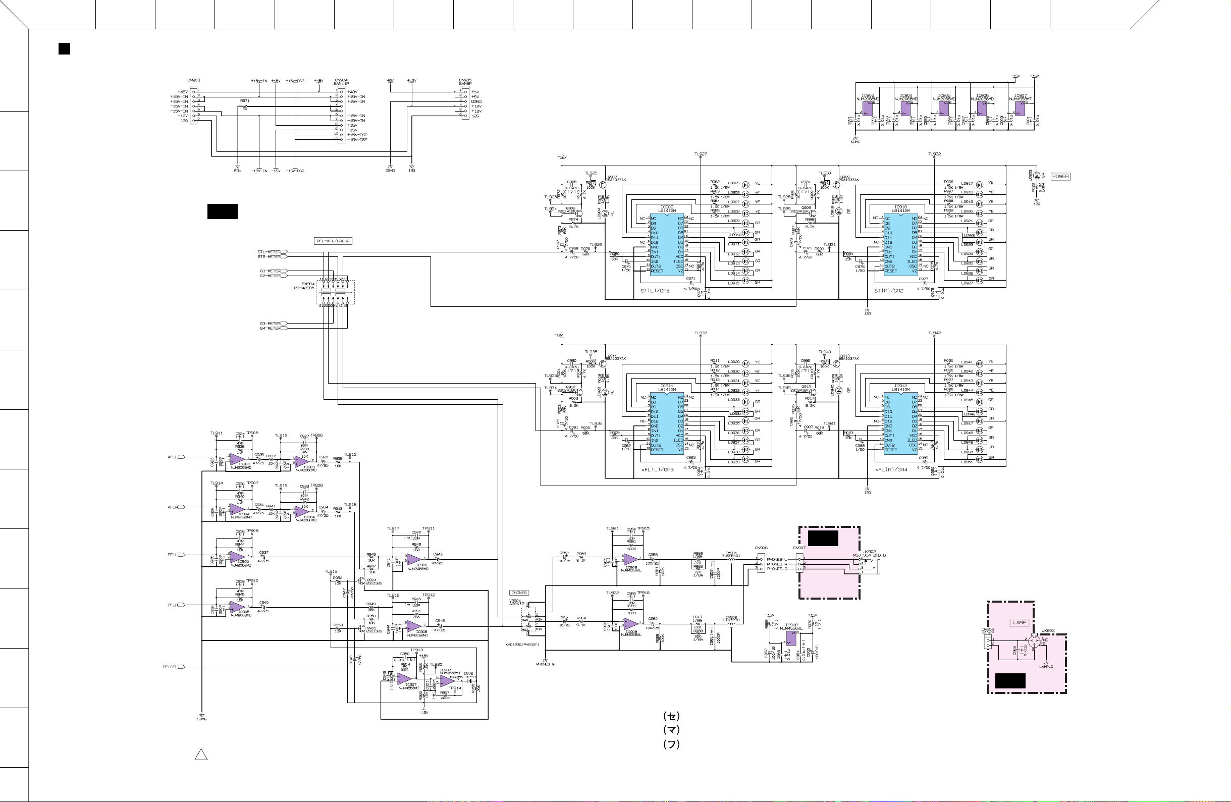
Page 48

ABCDEFGHIJKL
OVERALL CIRCUIT DIAGRAM 16/18 (MASJK)
MASJK
L (MONO)
ST CH INPUT
MG24/14FX: CH17 (L), 18 (R)
MG32/14FX: CH25 (L), 26 (R)
R
L (MONO)
ST CH INPUT
MG24/14FX: CH19 (L), 20 (R)
MG32/14FX: CH27 (L), 28 (R)
R
L (MONO)
RETURN1
+4dBu
R
L (MONO)
RETURN2
+4dBu
R
to MAS 1/4-CN101
(to Page 11)
to MAS 1/4-CN501
(to Page 14)
MG24/14FX
MG32/14FX
1
AUX1
AUX2
2
AUX3
to MAS 1/4-CN601
(to Page 16)
AUX4
3
SEND
+4dBu
AUX5
L
ST CH INPUT
MG24/14FX: CH21 (L), 22 (R)
MG32/14FX: CH29 (L), 30 (R)
R
RL
L
ST CH INPUT
MG24/14FX: CH23 (L), 24 (R)
MG32/14FX: CH31 (L), 32 (R)
R
2TR IN
-10dBV
RL
REC OUT
-10dBV
from Page 20: G6
from Page 20: G7
AUX6
EFF1
EFF2
4
5
6
7
28CC1-8828046-1
: Ceramic Capacitor
1
(
セラミックコンデンサー
)
19
8
Page 49

ABCDEFGHIJK
OVERALL CIRCUIT DIAGRAM 17/18 (MASJK)
1
MG24/14FX
MG32/14FX
MASJK
L
1
ST OUT
+4dBu
2
to MAS 1/4-CN701
(to Page 17)
2
GRPINS I/O
3
0dBu
to MAS 1/4-CN801
(to Page 17)
R
3
4
L
ST SUB OUT
+4dBu
R
4
5
to MAS 1/4-CN702
(to Page 17)
6
1
2
GROUP OUT
3
4
L
+4dBu
to Page 19: E6
ST INSERT I/O
to Page 19: E6
MONO
+4dBu
0dBu
7
not installed
*
Note: CN801 is not necessary to mount.
R
to MAS 1/4-CN502
FOOT SWITCH TAP
8
28CC1-8828046-2
20
1
Page 50
ABCDEFGHIJKLM
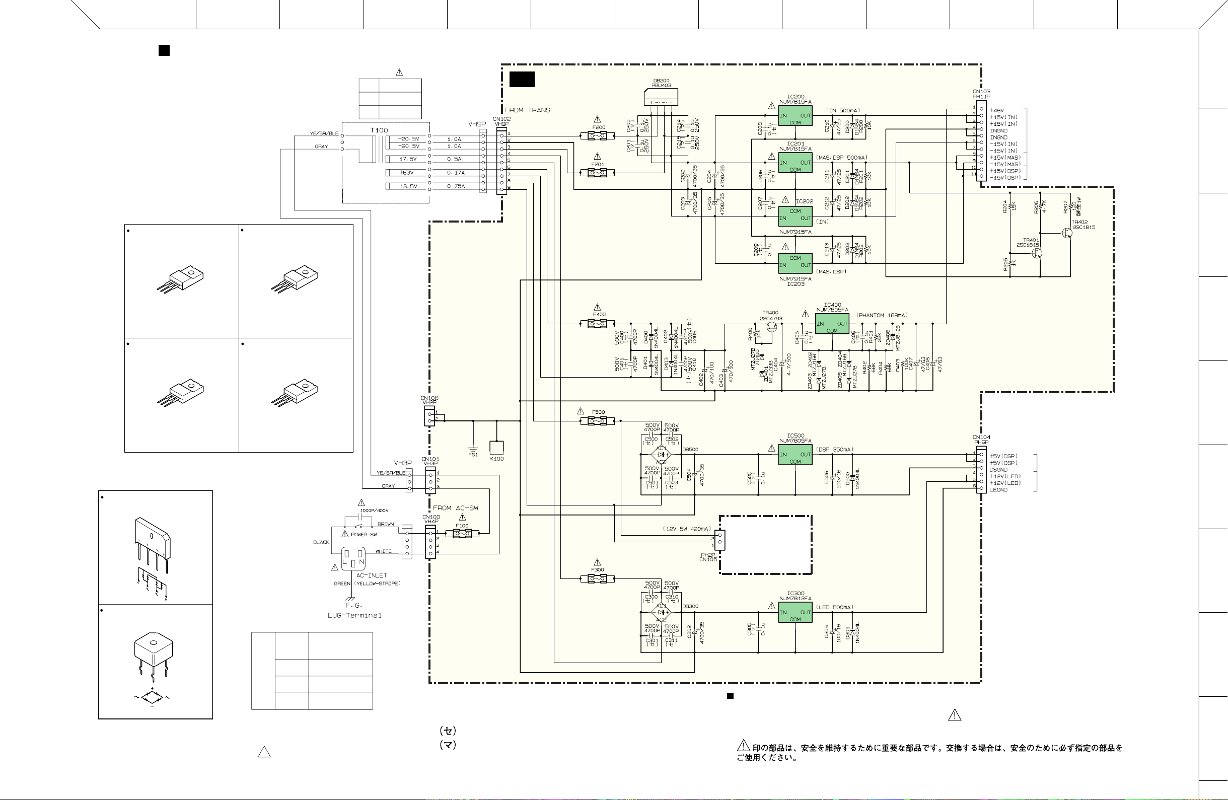
OVERALL CIRCUIT DIAGRAM 18/18 (PS)
NJM78M15FA(XJ603A00)
REGULATOR +15V
3
2
1
1: OUTPUT
2: COMMON
3: INPUT
NJM7812FA(XJ608A00)
REGULATOR +12V
NJM7915FA(XD854A00)
REGULATOR -15V
3
2
1
1: OUTPUT
2: INPUT
3: COMMON
NJM7805FA(XJ607A00)
REGULATOR +5V
TRANS
J
U/C
H/B
X3328B00
X3329B00
X3330B00
PS
DIODE STACK 4.0A
REGULATOR +15V
REGULATOR +15V
REGULATOR -15V
REGULATOR -15V
REGULATOR +5V
to MAS 1/4-CN904 (to Page 18)
to IN
to MAS
to DSP
MG24/14FX
MG32/14FX
1
2
3
4
3
2
1
PBU403 (VV518200)
DIODE STACK 4.0A 200V
S2VB20(IH001120)
DIODE STACK
28CC1-8828048
1: OUTPUT
2: COMMON
3: INPUT
FUSE
2
*
3
2
1
1: OUTPUT
2: COMMON
3: INPUT
REGULATOR +5V
to MAS 1/4-CN905 (to Page 18)
to DSP
to LED
to MAS 2/4-CN908
(to Page 18)
DIODE STACK
5
6
7
REGULATOR +12V
F100
F200
F201
F300
F400
F500
(KB000790)
T4AL 250V
(KB001660)
T1.6AL 250V
(KB002610)
T800mAL 250V
(KB000690)
T2.5AL 250V
*
Note: CN106 is not necessary to mount.
: Ceramic Capacitor
: Mylar Capacitor
: Metal Oxide Film Resistor
(
セラミックコンデンサー
(
マイラーコンデンサー
(酸化金属被膜抵抗)酸金
8
TO SERVICE PERSONNEL
Critical Components Information
Components having special characteristics are marked and must be replaced with parts having
)
)
specifications equal to those originally installed.
9
21
 Loading...