

YAMAHA MG206C MIX Diagram
SERVICE MANUAL
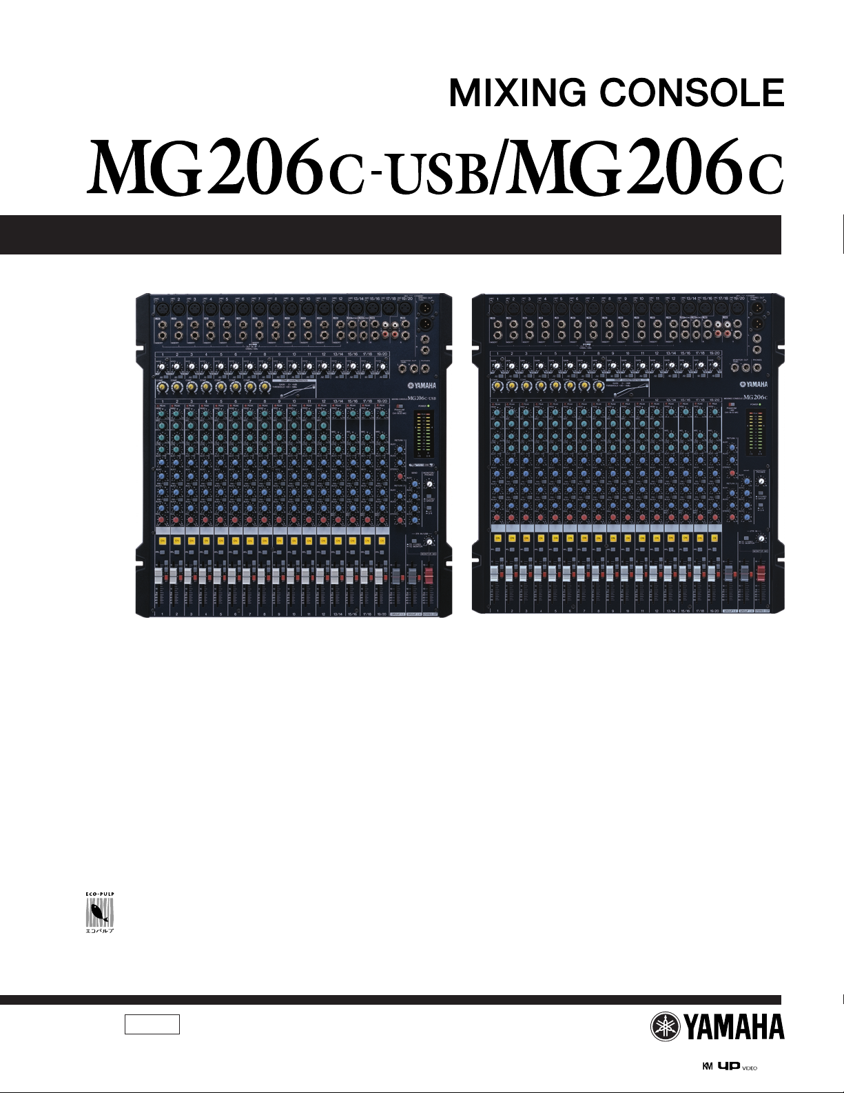
MG206C-USB MG206C
このサービスマニュアルはエコパルプ
(ECF:無塩素系漂白パルプ)を使用しています。
This document is printed on chlorine free (ECF) paper.
PA 011870
MG206C: 200708-94290
MG206C-USB: 200708-102690
■ CONTENTS (目次)
SPECIFICATIONS (総合仕様).................................................................. 3/5
DIMENSIONS (寸法図).............................................................................. 7
PANEL LAYOUT (パネルレイアウト)......................................................... 8
CIRCUIT BOARD LAYOUT (ユニットレイアウト).................................. 11
WIRING DIAGRAM (基板結線図)............................................................. 12
OVERALL ASSEMBLY WIRING (総組立配線図)........................................ 13
DISASSEMBLY PROCEDURES (分解手順)............................................. 19
LSI PIN DESCRIPTION (LSI端子機能表).................................................. 24
IC BLOCK DIAGRAM (ICブロック図)...................................................... 24
CIRCUIT BOARDS (シート基板図)........................................................... 27
INSPECTIONS (検査).......................................................................... 37/44
PARTS LIST
IC & DIODE FIGURES (外形図)
BLOCK & LEVEL DIAGRAM (ブロック&レベルダイアグラム)
CIRCUIT DIAGRAM (回路図)
HAMAMATSU, JAPAN
Copyright (c) Yamaha Corporation. All rights reserved. 07.08
MG206C-USB/MG206C
IMPORTANT NOTICE
This manual has been provided for the use of authorized Yamaha Retailers and their service personnel. It has been assumed that basic service
procedures inherent to the industry, and more specifically Yamaha Products, are already known and understood by the users, and have
therefore not been restated.
WARNING: Failure to follow appropriate service and safety procedures when servicing this product may result in personal injury, destruc-
tion of expensive components and failure of the product to perform as specified. For these reasons, we advise all Yamaha
product owners that all service required should be performed by an authorized Yamaha Retailer or the appointed service
representative.
IMPORTANT: This presentation or sale of this manual to any individual or firm does not constitute authorization, certification, recognition of
any applicable technical capabilities, or establish a principal-agent relationship of any form.
The data provided is believed to be accurate and applicable to the unit(s) indicated on the cover. The research engineering, and service
departments of Yamaha are continually striving to improve Yamaha products. Modifications are, therefore, inevitable and changes in specification are subject to change without notice or obligation to retrofit. Should any discrepancy appear to exist, please contact the distributor’s Service
Division.
WARNING: Static discharges can destroy expensive components. Discharge any static electricity your body may have accumulated by
IMPORTANT: Turn the unit OFF during disassembly and parts replacement. Recheck all work before you apply power to the unit.
grounding yourself to the ground bus in the unit (heavy gauge black wires connect to this bus).
WARNING: CHEMICAL CONTENT NOTICE!
The solder used in the production of this product contains LEAD. In addition, other electrical/electronic and/or plastic (Where applicable)
components may also contain traces of chemicals found by the California Health and Welfare Agency (and possibly other entities) to cause
cancer and/or birth defects or other reproductive harm.
DO NOT PLACE SOLDER, ELECTRICAL/ELECTRONIC OR PLASTIC COMPONENTS IN YOUR MOUTH FOR ANY REASON WHAT SO
EVER!
Avoid prolonged, unprotected contact between solder and your skin! When soldering, do not inhale solder fumes or expose eyes to solder/flux
vapor!
If you come in contact with solder or components located inside the enclosure of this product, wash your hands before handling food.
IMPORTANT NOTICE FOR THE UNITED KINGDOM
Connecting the Plug and Cord
WARNING: THIS APPARATUS MUST BE EARTHED
IMPORTANT. The wires in this mains lead are coloured in accordance with the following code:
As the colours of the wires in the mains lead of this apparatus may not correspond with the coloured markings identifying the terminals in your
plug, proceed as follows:
The wire which is coloured GREEN and YELLOW must be connected to the terminal in the plug which is marked by the letter E or by the safety
earth symbol or colored GREEN or colored GREEN and YELLOW.
The wire which is coloured BLUE must be connected to the terminal which is marked with the letter N or coloured BLACK.
The wire which is coloured BROWN must be connected to the terminal which is marked with the letter L or coloured RED.
GREEN-AND-YELLOW: EARTH
BLUE: NEUTRAL
BROWN: LIVE
■ WARNING
Components having special characteristics are marked and must be replaced with parts having specification equal to those originally
installed.
印の部品は、安全を維持するために重要な部品です。交換する場合は、安全のために必ず指定の部品をご使用ください。
2
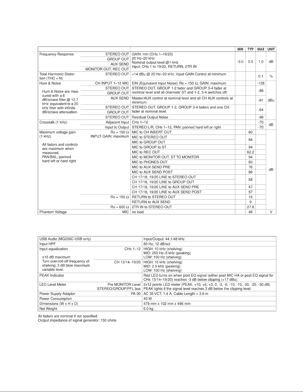
■ SPECIFICATIONS
• Electrical Specifications
MG206C-USB/MG206C
• General Specifications
3
MG206C-USB/MG206C
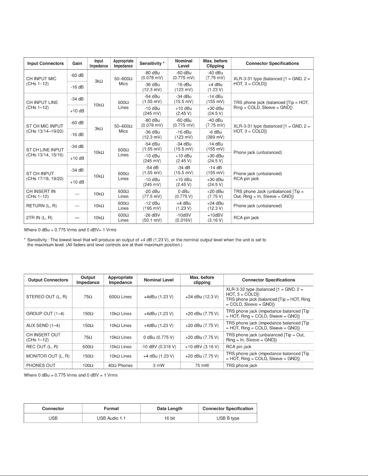
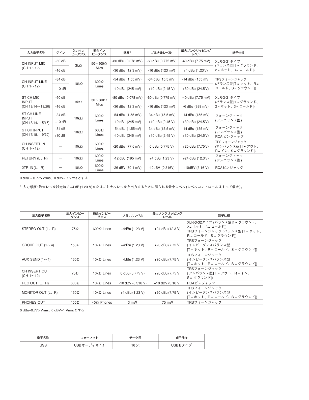
• Analog Input Specifications
• Analog Output Specifications
• Digital Input/Output Specifications (MG206C-USB only)
4
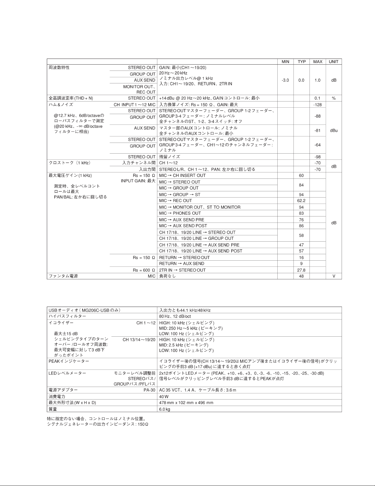
■ 総合仕様
・電気的特性
MG206C-USB/MG206C
・一般仕様
5
MG206C-USB/MG206C
・アナログ入力仕様
・アナログ出力仕様
・デジタル入出力仕様(MG206C-USBのみ)
6
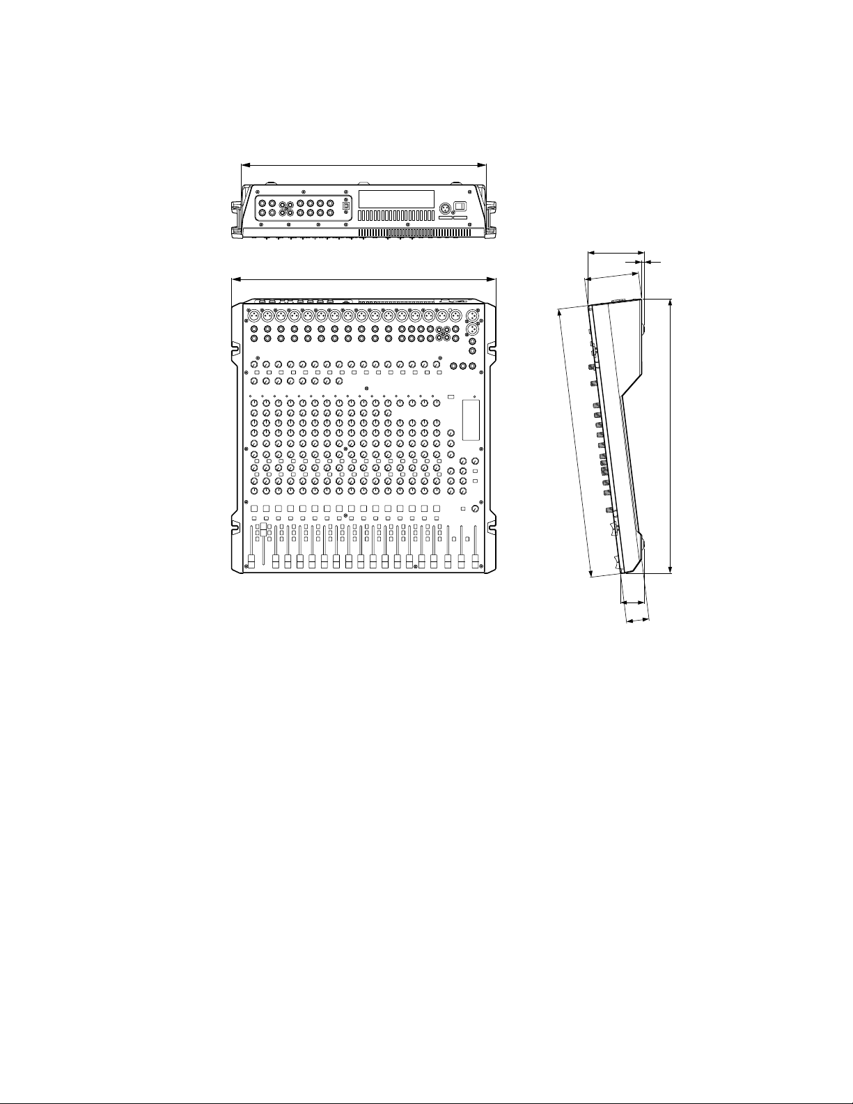
■ DIMENSIONS (寸法図)
MG206C-USB/MG206C
444
478
488.5
102
98
43
41
Unit: mm
単位:mm
5
496
MG206C-USB
7
MG206C-USB/MG206C
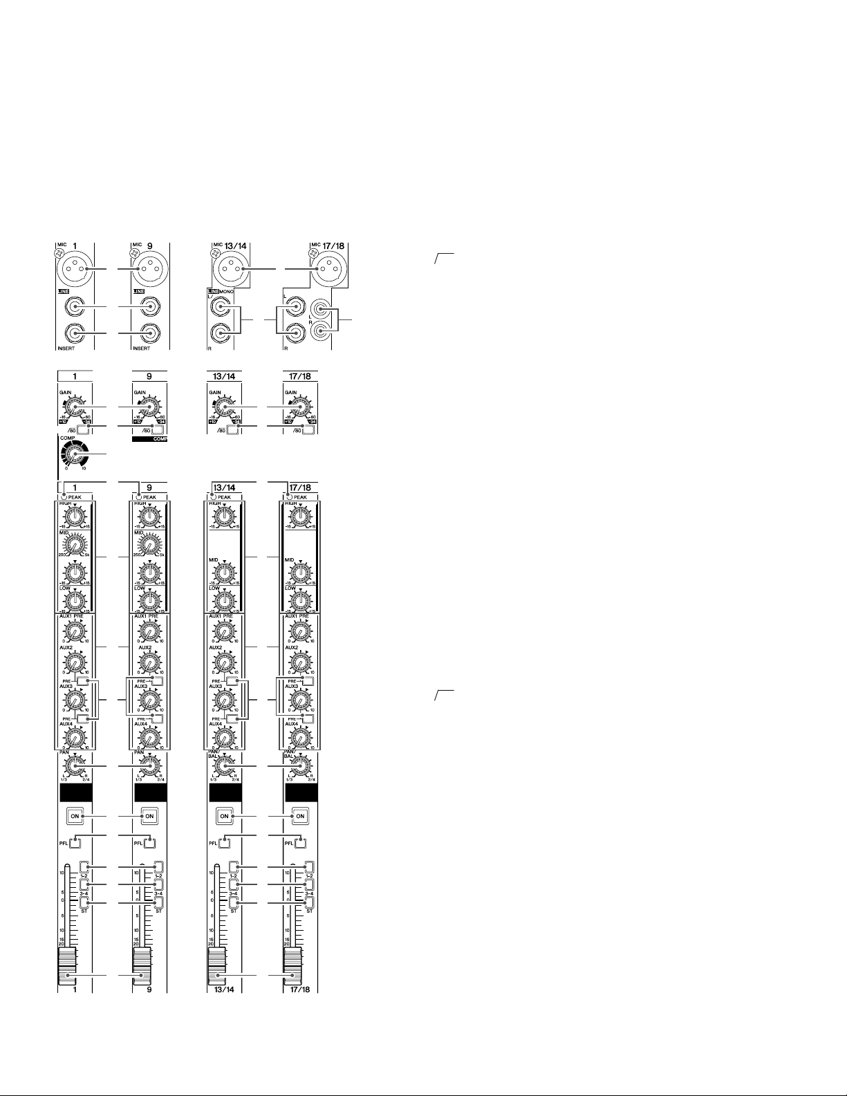
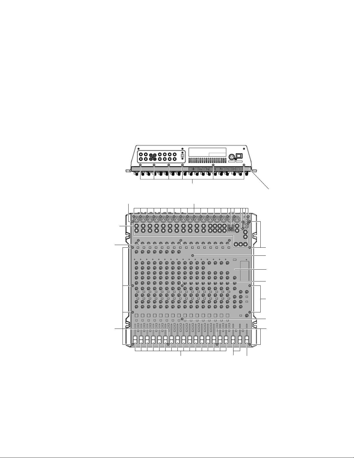
■ PANEL LAYOUT (パネルレイアウト)
• Channel Control Section (チャンネルコントロール部)
Channels
1 to 8
(Monaural)
チャンネル
1〜8
(モノラル)
Channels
9 to 12
(Monaural)
チャンネル
9〜12
(モノラル)
1
2
5
6 6
7 7
8
9 9
Channels
13/14 and 15/16
(Stereo)
チャンネル
13/14、15/16
(ステレオ)
3
Channels
17/18 and 19/20
(Stereo)
チャンネル
17/18、19/20
(ステレオ)
1
4
1
MIC Input Jacks
2
LINE Input Jacks (monaural channels)
3
LINE Input Jacks (stereo channels)
4
LINE Input Jacks (stereo channels)
5
INSERT Jacks
6
GAIN Control
7
80 Switch (High-Pass Filter)
8
COMP Control
9
PEAK Indicator
0
Equalizer (HIGH, MID and LOW)
A
AUX, EFFECT Control
B
AUX PRE Switch
C
PAN Control
PAN/BAL Control
BAL Control
D
ON Switch
E
PFL (Pre-Fader Listen) Switch
F
1-2 Switch
G
3-4 Switch
H
ST Switch
I
Channel Fader
0
A
0
A
BB
C C
D D
E E
F
G
H
F
G
H
1
MIC入力端子
2
LINE入力端子(モノラルチャンネル)
3
LINE入力端子(ステレオチャンネル)
4
LINE入力端子
5
INSERT端子
6
GAINコントロール
7
80(ハイパスフィルター)スイッチ
8
COMPコントロール
9
PEAKインジケーター
0
EQ(イコライザー:HIGH、MID、LOW)
A
AUX、EFFECTコントロール
B
AUXPREスイッチ
C
PANコントロール
PAN/BALコントロール
BALコントロール
D
ONスイッチ
E
PFLスイッチ
F
1-2スイッチ
G
3-4スイッチ
H
STスイッチ
I
チャンネルフェーダー
I I
8
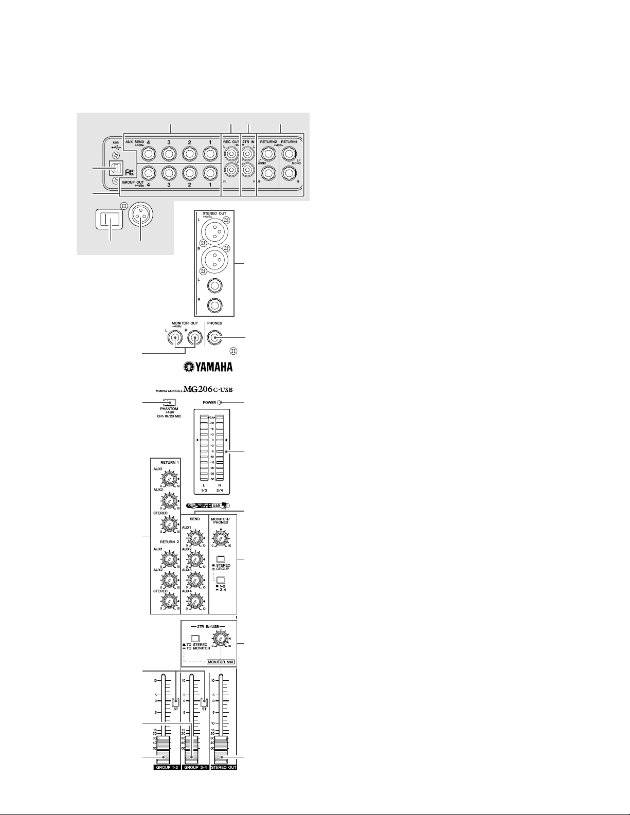
• Master Control Section (マスターコントロール部)
Rear panel
6542
1
3
K L
7
9
8
0
A
B
D
C
E
F
I
H
G
J
MG206C-USB/MG206C
1
USB Connector (MG206C-USB only)
2
SEND Jacks (AUX, EFFECT)
3
GROUP OUT (1 to 4) Jacks
4
REC OUT (L, R) Jacks
5
2TR IN Jacks
6
RETURN L (MONO), R Jacks
7
STEREO OUT (L, R) Jacks
• XLR Jacks
• LINE Jacks
8
MONITOR OUT Jacks
9
PHONES Jack
0
PHANTOM +48 V Switch
A
POWER Indicator
B
Level Meter
C
RETURN
• AUX1, AUX2 Control
• STEREO Control
D
Master SEND Controls (AUX, EFFECT)
E
MONITOR/PHONES
• MONITOR Switches
• MONITOR Control
F
2TR IN (MG206C)
2TR IN/USB (MG206C-USB)
• 2TR IN/USB Switch
• 2TR IN/USB Control
G
GROUP 1-2 Fader
H
GROUP 3-4 Fader
I
ST Switch
J
STEREO OUT Master Fader
K
POWER Switch
L
AC ADAPTOR IN Connector
1
USB端子(MG206C-USBのみ)
2
SEND端子(AUX、EFFECT)
3
GROUPOUT(1-4)端子
4
RECOUT(L、R)端子
5
2TRIN端子
6
RETURNL(MONO)、R端子
7
STEREOOUT(L、R)端子
・ XLR端子
・ LINE端子
8
MONITOROUT端子
9
PHONES端子
0
PHANTOM+48Vスイッチ
A
POWERインジケーター
B
レベルメーター
C
RETURN
・ AUX1、2コントロール
・ STEREOコントロール
D
SENDマスターコントロール(AUX、EFFECT)
E
MONITOR/PHONES
・ モニター信号切り替えスイッチ
・ モニターコントロール
F
2TRIN(MG206C)
2TRIN/USB(MG206C-USB)
・ 出力先切り替えスイッチ
・ 2TRIN/USBコントロール
G
GROUP1-2フェーダー
H
GROUP3-4フェーダー
I
STスイッチ
J
STEREOOUTマスターフェーダー
K
電源スイッチ
L
ACADAPTORIN端子
9
MG206C-USB/MG206C
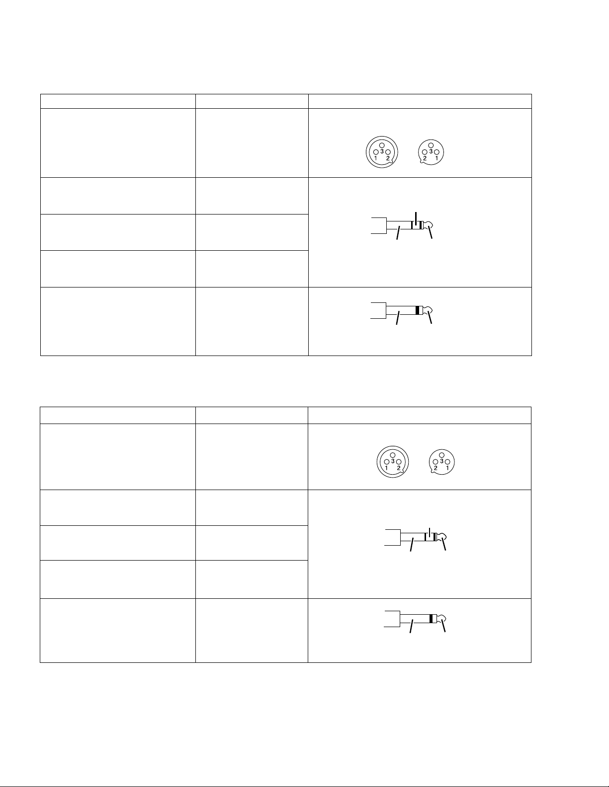
• Connector Polarities
Input and Output Jacks Polarities Configurations
MIC INPUT, STEREO OUT
LINE INPUT (monaural channels)
GROUP OUT, STEREO OUT,
MONITOR OUT, AUX SEND
INSERT
PHONES
RETURN
LINE INPUT (stereo channels)
• 端子接続の極性
入出力端子名 端子の極性 端子の形状
Pin 1: Ground
Pin 2: Hot (+)
Pin 3: Cold (–)
Tip: Hot (+)
Ring: Cold (–)
Sleeve: Ground
Tip: Output
Ring: Input
Sleeve: Ground
Tip: L
Ring: R
Sleeve: Ground
Tip: Hot
Sleeve: Ground
OUTPUTINPUT
XLR Jack
Ring
TipSleeve
TRS Phone Jack
TipSleeve
Phone Jack
MIC INPUT、STEREO OUT
LINE INPUT(モノラルチャンネル)
GROUP OUT、STEREO OUT、
MONITOR OUT、AUX SEND
INSERT
PHONES
RETURN
LINE INPUT(ステレオチャンネル)
ピン1:グラウンド
ピン2:ホット(+)
ピン3:コールド(–)
チップ:ホット(+)
リング:コールド(–)
スリーブ:グラウンド
チップ:Output
リング:Input
スリーブ:グラウンド
チップ:L
リング:R
スリーブ:グラウンド
チップ:ホット
スリーブ:グラウンド
OUTPUTINPUT
リング
リング
チップスリーブ
チップスリーブ
チップスリーブ
XLR端子
TRSフォーン端子
フォーン端子
10
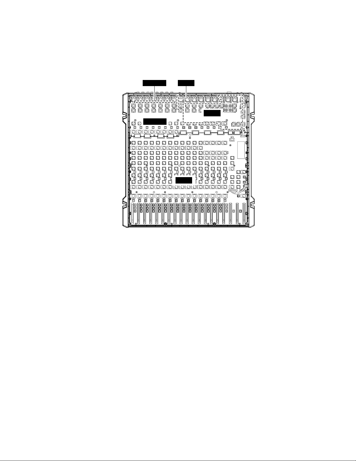
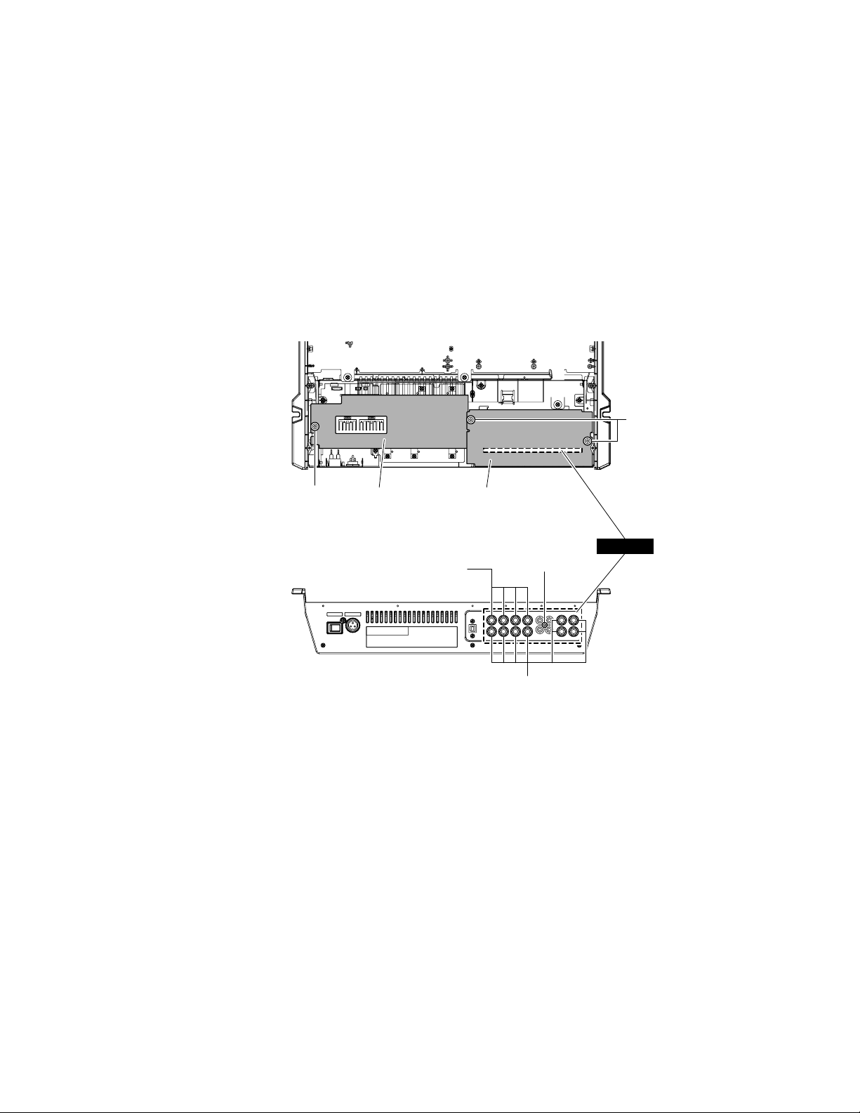
■ CIRCUIT BOARD LAYOUT (ユニットレイアウト)
Rear
(リア)
MG206C-USB/MG206C
JACK20R
JACK20F
USB
(MG206C-USB only)
MIX20
Front
(フロント)
PS20
11
MG206C-USB/MG206C
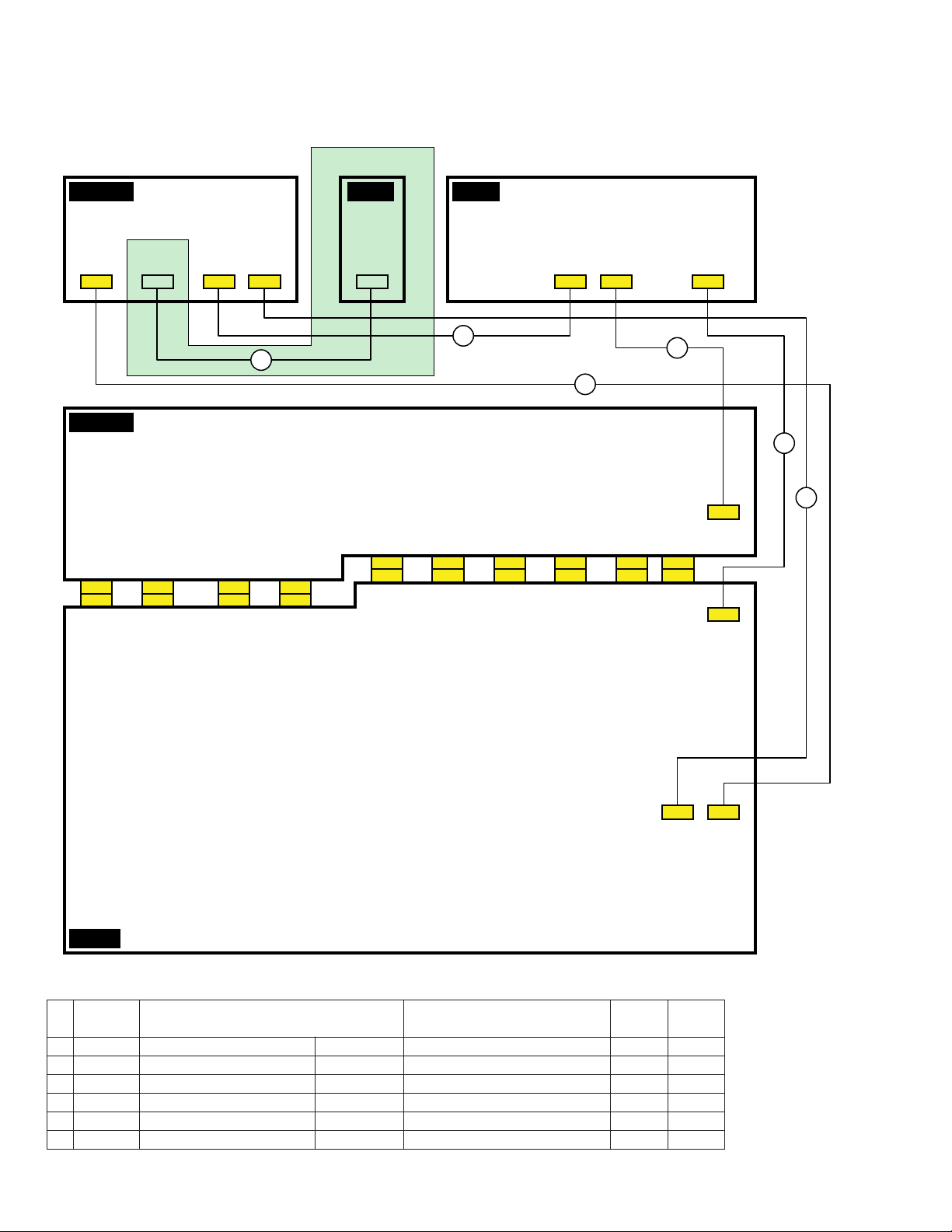
■ WIRING DIAGRAM (基板結線図)
(MG206C-USB only)
JACK20R
CN003
(10P)
JACK20F
W101
(9P)
CN101
(9P)
CN903
(9P)
W201
(9P)
CN201
(9P)
CN002
(2P)
W301
(9P)
CN301
(9P)
CN004
(15P)
4
W401
(9P)
CN401
(9P)
CN101
(9P)
W501
(9P)
CN501
(9P)
W601
(9P)
CN601
(9P)
PS20USB
CN103
CN102
(2P)
(3P)
3
5
W701
(9P)
CN701
(9P)
W801
(9P)
CN801
(9P)
W001
(6P)
CN001
(6P)
2
W002
(9P)
CN002
(9P)
CN101
(7P)
CN001
(3P)
CN053
(7P)
1
6
MIX20
No. Part No.
1
(WJ98020)
2
(WJ98040)
3
(WJ98050)
4
(WJ78450)
5
(WJ78460)
6
(WJ78470)
12
Assembly Name
線材名
Connector Assembly PS7P
Connector Assembly PS3P
Connector Assembly PS2P
Connector Assembly USB20
Connector Assembly REAR10P
Connector Assembly REAR15P
PS7P束線
PS3P束線
PS2P束線
USB20束線
REAR10P束線
REAR15P束線
Connection
接続
MIX20-CN053 <-> PS20-CN101
JACK20F-CN001 <-> PS20-CN102
JACK20R-CN002 <-> PS20-CN103
JACK20R-CN903 <-> USB-CN101
MIX20-CN003 <-> JACK20R-CN003
MIX20-CN004 <-> JACK20R-CN004
Remarks
備考
7P-110
3P-140
2P-380
9P-140
10P-700
15P-720
CN004
(15P)
Location
100
130
140
CN003
(10P)
40
50
60
MG206C-USB only
MG206C-USB/MG206C
■ OVERALL ASSEMBLY WIRING (総組立配線図)
The inside room of this product is very little because a lot of units are installed fully.
To prevent the panel’s coming up and other things when assembling, perform the cable connection according to the followings.
(このモデルは、ユニットの集積度が高く、内部スペースに余裕がありません。
組み立て時のパネル浮き等を防止する為に、束線処理は下記のように行なってください。)
Note: The components marked “ * ” are used only for MG206C-USB.
(注:*マークの部品はMG206C-USBのみに使用されています。)
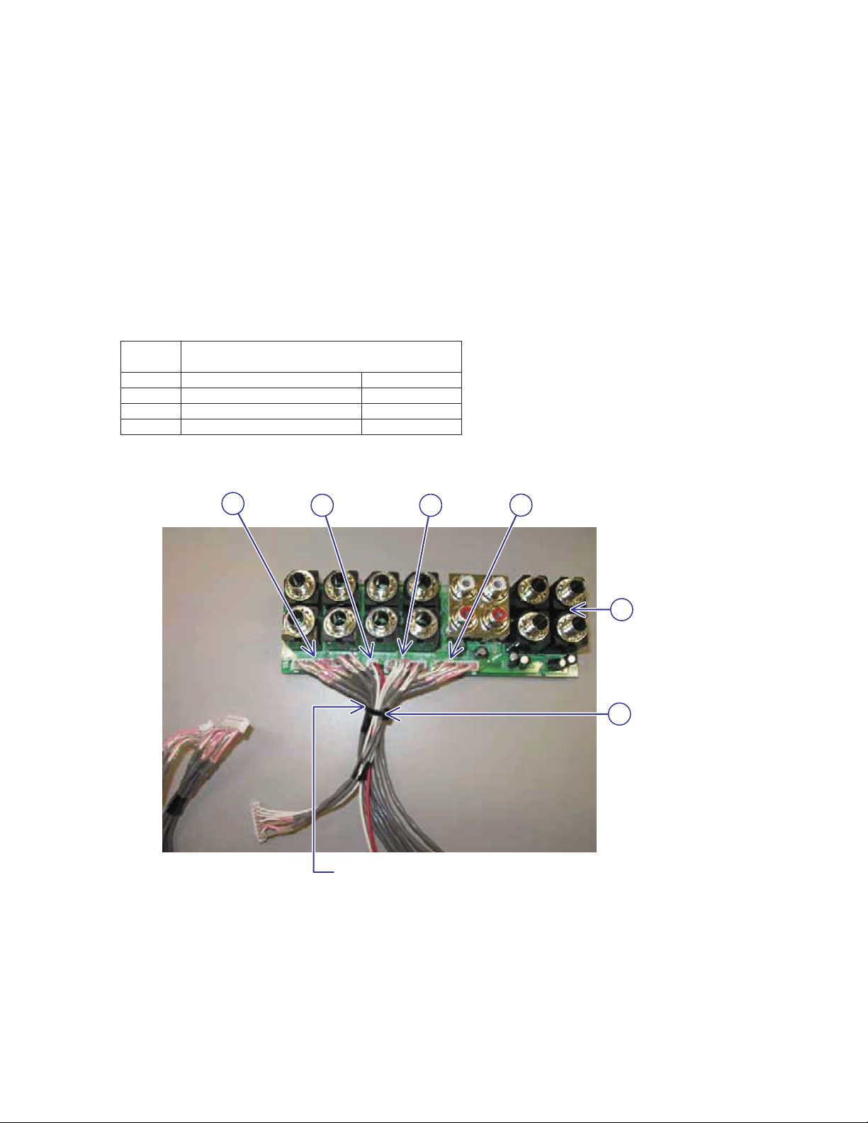
1. The wiring of the Inner Chassis Assembly. (インナーシャーシAssyの配線)
1-1. Before installing the JACK20R [Ref. 120] circuit board in the inner chassis Assembly [Ref. 20], connect the following connector
assemblies to the JACK20R [Ref. 120] circuit board and bind the connector assemblies with the cord binder [Ref. 180].
(インナーシャーシAssy[Ref.20]に取り付ける前に、JACK20Rシート[Ref.120]に下記の束線を取り付け、インシュロック
タイ[Ref.180]で結束します。)
Ref. No.
60
100 *
130
140
Connector Assembly Name
線材名
Connector Assembly PS2P
Connector Assembly USB20
Connector Assembly REAR10P
Connector Assembly REAR15P
CN004
140
CN002 CN903
60 100
PS2P束線
USB20束線
REAR10P束線
REAR15P束線
*
CN003
130
120
180
Note: Binding position
BindattheendoftapeontheconnectorassemblyRear15P[Ref.140].
(注: 結束位置
REAR15P束線[Ref.140]上のテープ端を目安として結束します。)
13
MG206C-USB/MG206C
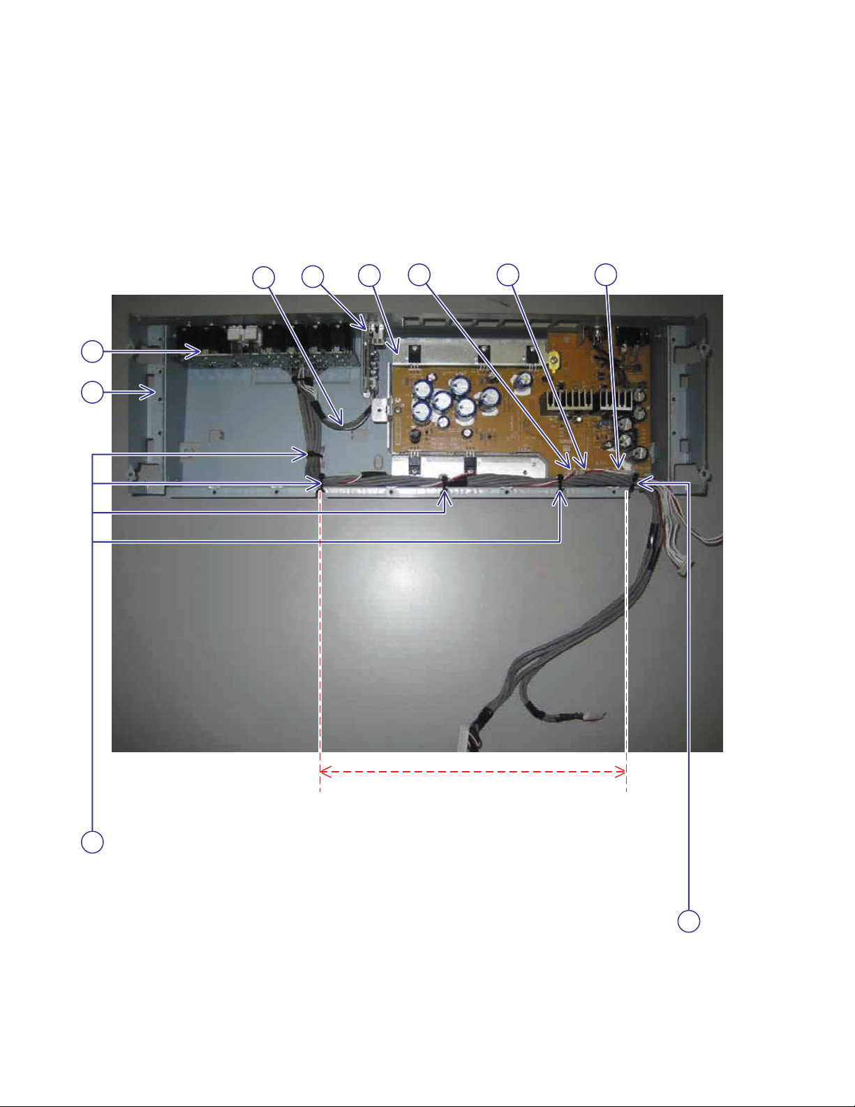
1-2. Install the heatsink assembly [Ref. 30], USB assembly [* Ref. 90] and JACK20R circuit board [Ref. 120] in the inner chassis
assembly [Ref. 20].
(ヒートシンクAssy[Ref.30]、USBAssy[*Ref.90]、JACK20Rシート[Ref.120]をインナーシャーシAssy[Ref.20]に
取り付けます。)
1-3. Connect the connector assemblies according to the picture below.
(下記の写真に従って配線します。)
120
20
CN103
*
*
100
90
30
60
CN102
50
CN101
40
14
Note: Twist connector assemblies three times in this section.
(注: この区間で、束線を3回ねじってください。)
180
Note: Fix the connector assembly PS2P [Ref. 60], connector assembly REAR10P [Ref. 130] and connector
assembly REAR15P [Ref. 140] with the cord binder [Ref. 180].
(注: PS2P束線[Ref.60]とREAR10P束線[Ref.130]とREAR15P束線[Ref.140]をインシュロックタイ[Ref.
180]で固定します。)
Note: Fix the connector assembly REAR10P [Ref. 130], connector assembly REAR15P [Ref. 140], connector
assembly PS7P [Ref. 40] and connector assembly PS3P [Ref. 50] with the cord binder [Ref. 180].
(注: REAR10P束線[Ref.130]、REAR15P束線[Ref.140]、PS7P束線[Ref.40]、PS3P束線[Ref.50]をイ
ンシュロックタイ[Ref.180]で固定します。)
180
1-4. Install the inner chassis assembly [Ref. 20] on the bottom case assembly [Ref. 10].
(インナーシャーシAssy[Ref.20]をボトムケースAssy[Ref.10]に取り付けます。)
20 10 40 50
MG206C-USB/MG206C
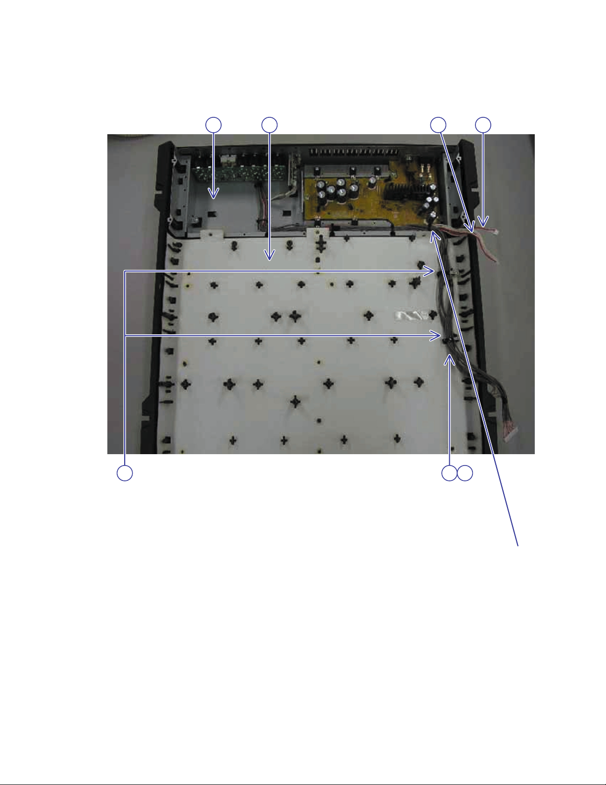
Note: Fix the connector assembly REAR10P [Ref. 130] and connector assem-
bly REAR15P [Ref. 140] with the cord holder [Ref. 230].
(注: REAR10P束線[Ref.130]とREAR15P束線[Ref.140]を束線止め[Ref.
230]で固定します。)
Note: Pass the connector assembly REAR10P [Ref. 130] and connector assembly REAR15P [Ref. 140] through
the incision part of inner chassis assembly [Ref. 20]. At that time, take care the cables not to be slackened.
(注: REAR10P束線[Ref.130]とREAR15P束線[Ref.140]を、インナーシャーシAssy[Ref.20]の切り欠き
へ通します。その時、線材がたるまないように注意してください。)
130 140230
15
MG206C-USB/MG206C
2. The wiring of the MIX20 circuit board and JACK20F circuit board.
(MIX20シートとJACK20Fシートの配線)
Whole picture (全体写真)
250
MIX20
CN101
MIX20
CN201
MIX20
CN301
MIX20
CN401
MIX20
CN501
MIX20
CN601
MIX20
CN701
MIX20
CN801
JACK20F
CN001
MIX20
CN001
JACK20F
MIX20
CN002
MIX20
K052
K101
50
40
MIX20
CN053
MIX20
K051
16
340
140
MIX20
CN004
MIX20
CN003
130
2-1. Connect the connector assemblies from the inner chassis assembly.
(インナーシャーシAssyからの束線を配線します。)
MG206C-USB/MG206C
Final Assembly
Location
Ref. 40
Ref. 50
Ref. 130
Ref. 140
Connector Assembly PS7P
Connector Assembly PS3P
Connector Assembly REAR10P
Connector Assembly REAR15P
Connector Assembly Name
線材名
PS7P束線
PS3P束線
REAR10P束線
REAR15P束線
Wiring Point
MIX20 circuit board CN053
JACK20F circuit board CN001
MIX20 circuit board CN003
MIX20 circuit board CN004
Macro picture around CN053 on the MIX20 circuit board. (MIX20シートCN053周辺の拡大写真)
250
50
JACK20F
CN001
340
40
MIX20
CN053
JACK20F
K101
Note: Fix the connector assembly PS7P [Ref. 40] and connector assembly
[Ref. 50] with the cord holder.
(注: PS7P束線[Ref.40]とPS3P束線[Ref.50]を束線止めで固定します。)
Note: Pass the connector assembly PS7P [Ref. 40] and connector assembly PS3P [Ref. 50] through the inci-
sion part of JACK20F circuit board [Ref. 250].
(注: PS7P束線[Ref.40]とPS3P束線[Ref.50]をJACK20Fシート[Ref.250]の切り欠きへ通します。)
17
MG206C-USB/MG206C
Macro picture around the CN003 of MIX20 circuit board. (MIX20シートCN003周辺の拡大写真)
Note: Pass the connector assembly REAR10P [Ref. 130] and connector as-
sembly REAR15P [Ref. 140] through the incision part of MIX20 circuit
board [Ref. 340].
(注: REAR10P束線[Ref.130]とREAR15P束線[Ref.140]を、MIX20シート
[Ref.340]の切り欠きへ通します。)
340
MIX20
CN004
130
MIX20
140
MIX20
K052
Note: Fix the connector assembly REAR15P [Ref.
140] with the cord holder.
(注: REAR15P束線[Ref.140]を束線止めで固定
します。)
CN003
MIX20
K051
Note: Fix the connector assembly REAR10P [Ref. 130] with
the cord holder.
(注: REAR10P束線[Ref.130]を束線止めで固定します。)
2-2. Connect the ten (10) jumper wires of JACK20F circuit board to the MIX20 circuit board.
(JACK20Fシートのジャンパーワイヤー10本をMIX20シートへ接続します。)
Note: Bend the jumper wires according to the picture below.
(注: 下記の写真に従ってジャンパーワイヤーを折り曲げます。)
Note: After bend, press the jumper wires so that their height from the MIX20 circuit board’s component side become 15 mm or less.
(注: 折り曲げ後、ジャンパーワイヤーがMIX20シート面から15mm以下になるように上から押します。)
18
■ DISASSEMBLY PROCEDURES (分解手順)
MG206C-USB/MG206C
1. Top Cover (Time required: 15 min.)
1-1 Remove the sixteen (16) fader knobs marked [490], two
(2) fader knobs marked [500] and fader knob marked
[510]. (Fig. 1)
1-2 Remove the fifteen (15) screws marked [400], twenty-
one (21) screws marked [410], three (3) screws marked
[420], six (6) screws marked [430], thirty-seven (37) hexagonal nuts and thirty-seven (37) washers. (Fig. 1)
1-3 The top cover can then be removed. (Fig. 1)
* When installing the top cover on the bottom case
assembly, tighten the screws in the order shown in
Fig. 1. (Fig. 1)
[400]
1. トップカバー(所要時間:15分)
1-1 [490]のノブFADER16個、[500]のノブFADER2個、
[510]のノブFADERを外します。(Fig.1)
1-2 [400]のネジ15本、[410]のネジ21本、[420]のネジ3
本、[430]のネジ6本、六角ナット37個、ワッシャー37
個を外します。(Fig.1)
1-3 トップカバーを外します。(Fig.1)
* トップカバーをボトムAssyへ取り付けるときは、
Fig. 1で示した順序でネジ締めしてください。
(Fig.1)
[430]
Top cover
[410]
(トップカバー)
M9 Hexagon nut and washer
(M9六角ナット、ワッシャー)
[420]
[400]
[400]: Bind Head Tapping Screw-B 3x8 MFZN2B3 (WE774400) Bタイト+BIND
[410]: Bind Head Tapping Screw-B 3x8 MFZN2B3 (WE774400) Bタイト+BIND
[420]: Bind Head Screw 3x6 MFZN2B3 (WE878300) 小ネジ+BIND
[430]: Bind Head Tapping Screw-B 3x8 MFZN2B3 (WE774400) Bタイト+BIND
[490]: Fader Knob Black/L-Gray (V9664900) ノブFADER
[500]: Fader Knob Red/D-Gray (V9665000) ノブFADER
[510]: Fader Knob White/Red (V9665100) ノブFADER
[490] [500] [510]
[400]
[400] Screw tighten (3rd)
(ネジ締め(3番))
Top cover
(トップカバー)
Screw tighten (1st)
[400]
(ネジ締め(1番))
[400]
Screw tighten (2nd)
[400]
(ネジ締め(2番))
[400]
(Fig. 1)
19
MG206C-USB/MG206C
2. MIX20 Circuit Board and JACK20F Circuit
Board (Time required: 20 min.)
2-1 Remove the top cover. (See procedure 1.)
2-2 Disconnect the fourteen (14) connectors. (Fig. 2)
2-3 Remove the fourteen (14) screws marked [350]. (Fig. 2)
2-4 Release the eight (8) hooks and remove the MIX20 cir-
cuit board. (Fig. 2)
2-5 Remove the three (3) screws marked [300] and remove
the JACK20F circuit board. (Fig. 2)
* The buttons, knobs, knob black (WD942200), but-
ton on assembly (WH455200) are not components
of the MIX20 circuit board. When replacing the MIX20
circuit board, remove these components from the
old circuit board and install them on the new circuit
board.
[300]
2. MIX20シート、JACK20Fシート (所要時間:20分)
2-1 トップカバーを外します。(1項参照)
2-2 14ヶ所のコネクターを外します。(Fig.2)
2-3 [350]のネジ14本を外します。(Fig.2)
2-4 8ヶ所のフックを外し、MIX20シートを外します。(Fig.2)
2-5 [300]のネジ3本を外し、JACK20Fシートを外します。
(Fig.2)
* ボタン、ノブ類、ノブ継ぎ手HPF(WD942200)、ボ
タンONAssy(WH455200)などはMIX20シートの構
成部品ではありません。MIX20シート交換時は、旧
シートからこれらの部品を取り外して新しいシート
に取り付けてください。
JACK20F
[350]
(フック)
Priority Screw
(優先ネジ)
(フック)
(フック)
[300]: Bind Head Tapping Screw-B 3x8 MFZN2W3 (WE774300) Bタイト+BIND
[350]: Bind Head Tapping Screw-B 3x8 MFZN2W3 (WE774300) Bタイト+BIND
Hook
[350]
Hook
[350]
Hook
(Fig. 2)
MIX20
[350]
Hook
(フック)
[350]
Hook
(フック)
20
MG206C-USB/MG206C
3. JACK20R Circuit Board (Time required: 25 min.)
3-1 Remove the top cover. (See procedure 1.)
3-2 Remove the MIX20 circuit board and JACK20F circuit
board. (See procedure 2.)
3-3 Remove the two (2) screws marked [170A] and remove
the rear JK shield. (Fig. 3)
3-4 Remove the screw marked [150], twelve (12) hexago-
nal nuts and twelve (12) washers. (Fig. 3)
The JACK20R circuit board can then be removed. (Fig. 3)
[170B]
Shield PS
(シールドPS)
(リアJKシールド)
3. JACK20Rシート(所要時間:25分)
3-1 トップカバーを外します。(1項参照)
3-2 MIX20シート、JACK20Fシートを外します。(2項参照)
3-3 [170A]のネジ2本を外し、リアJKシールドを外します。
(Fig.3)
3-4 [150]のネジ、六角ナット12個、ワッシャー12個を外
し、JACK20Rシートを外します。(Fig.3)
[170A]
Rear JK shield
M9 Hexagon nut and washer
(M9六角ナット、ワッシャー)
[150]: Bind Head Tapping Screw-B 3x8 MFZN2B3 (WE774400) Bタイト+BIND
[170A]: PW Head Tapping Screw-B 3x8 MFZN2W3 (WF002600) Bタイト+PWH
[170B]: PW Head Tapping Screw-B 3x8 MFZN2W3 (WF002600) Bタイト+PWH
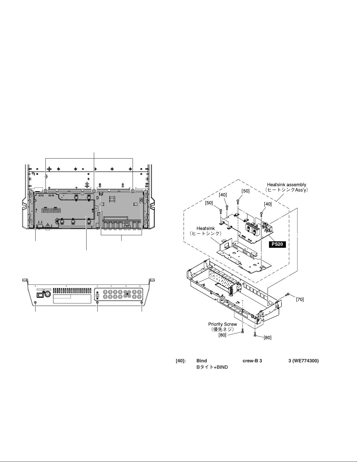
4. PS20 Circuit Board (Time required: 25 min.)
4-1 Remove the top cover. (See procedure 1.)
4-2 Remove the MIX20 circuit board and JACK20F circuit
board. (See procedure 2.)
4-3 Remove the two (2) screws marked [170A] and remove
the rear JK shield. (Fig. 3)
4-4 Remove the screw marked [170B] and remove the shield
PS. (Fig. 3)
Priority Screw
(優先ネジ)
[150]
M9 Hexagon nut and washer
(M9六角ナット、ワッシャー)
JACK20R
(Fig. 3)
4. PS20シート(所要時間:25分)
4-1 トップカバーを外します。(1項参照)
4-2 MIX20シート、JACK20Fシートを外します。(2項参照)
4-3 [170A]のネジ2本を外し、リアJKシールドを外します。
(Fig.3)
4-4 [170B]のネジを外し、シールドPSを外します。(Fig.3)
21
MG206C-USB/MG206C
4-5 Remove the three (3) screws marked [190], three (3)
screws marked [200] and three (3) screws marked [220].
(Fig. 4)
The inner chassis with heatsink assembly, JACK20R
circuit board and USB assembly (MG206C-USB only)
can be removed. (Fig. 4)
4-6 Disconnect the three (3) connectors. (Fig. 4)
4-7 Remove the four (4) screws marked [80] and screw marked
[70]. Then remove the heatsink assembly. (Fig. 5)
4-8 Remove the three (3) screws marked [40] and five (5)
screws marked [50], and separate the PS20 circuit board
from the heatsink. (Fig. 5)
[220]
4-5 [190]のネジ3本、[200]のネジ3本、[220]のネジ3本を外
し、インナーシャーシ(ヒートシンクAssy、JACK20R
シート、USBAssy【MG206C-USBのみ】付き)を外しま
す。(Fig.4)
4-6 3ヶ所のコネクターを外します。(Fig.4)
4-7 [80]のネジ4本、[70]のネジを外し、ヒートシンクAss
yを外します。(Fig.5)
4-8 [40]のネジ3本、[50]のネジ5本を外し、PS20シートと
ヒートシンクを分離します。(Fig.5)
Heatsink assembly
(ヒートシンクAss'y)
[40]
[50]
[40]
[50]
[200]
Inner chassis with heatsink assembly, JACK20R circuit boad
(インナーシャーシ[ヒートシンクAss'y、JACK20Rシート、
[190]: Bind Head Tapping Screw-B 3x8 MFZN2B3 (WE774400)
[200]: Bind Head Tapping Screw-B 3x8 MFZN2W3 (WE774300)
[220]: PW Head Tapping Screw-B 3x8 MFZN2W3 (WF002600)
and USB assembly (MG206C-USB only)
USBAss'y【MG206C-USBのみ】付き])
[190] [190]
Bタイト+BIND
Bタイト+BIND
Bタイト+PWH
[190]
Priority Screw
(優先ネジ)
[200]
(Fig. 4)
Heatsink
(ヒートシンク)
PS20
[70]
Priority Screw
(優先ネジ)
[80]
[40]: Bind Head Tapping Screw-B 3x8 MFZN2W3 (WE774300)
Bタイト+BIND
[50]: Bind Head Tapping Screw-B 3x8 MFZN2W3 (WE774300)
Bタイト+BIND
[70]: Bind Head Tapping Screw-B 3x8 MFZN2B3 (WE774400)
Bタイト+BIND
[80]: Bind Head Tapping Screw-B 3x8 MFZN2W3 (WE774300)
Bタイト+BIND
[80]
22
(Fig. 5)
MG206C-USB/MG206C
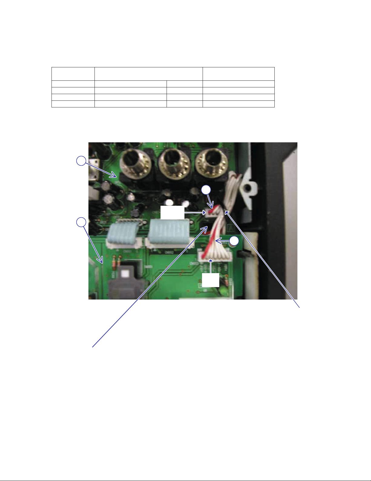
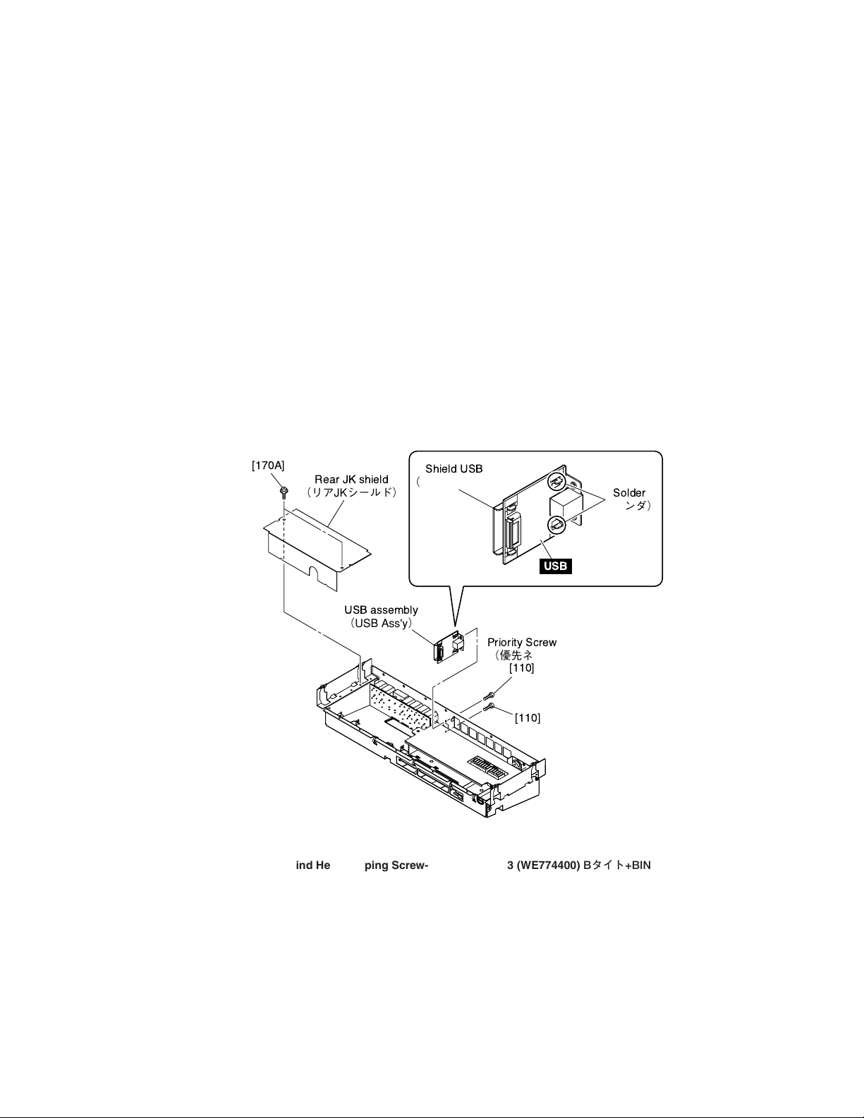
5. USB Circuit Board (MG206C-USB only)
(Time required: 20 min.)
5-1 Remove the top cover. (See procedure 1.)
5-2 Remove the MIX20 circuit board and JACK20F circuit
board. (See procedure 2.)
5-3 Remove the two (2) screws marked [170A] and remove
the rear JK shield. (Fig. 6)
5-4 Remove the two (2) screws marked [110] and remove
the USB assembly. (Fig. 6)
5-5 Unsolder the shield USB mounting solder (2 locations)
and separate the shield USB from the USB circuit board.
(Fig. 6)
* The shield USB is not a component of the USB cir-
cuit board. When replacing the USB circuit board,
remove the shield USB from the old circuit board
and install it on the new circuit board.
[170A]
Rear JK shield
(リアJKシールド)
Shield USB
(シールドUSB)
5. USBシート(MG206C-USBのみ)
(所要時間:20分)
5-1 トップカバーを外します。(1項参照)
5-2 MIX20シート、JACK20Fシートを外します。(2項参照)
5-3 [170A]のネジ2本を外し、リアJKシールドを外します。
(Fig.6)
5-4 [110]のネジ2本を外し、USBAss'yを外します。(Fig.6)
5-5 2ヶ所のハンダ付けを外し、USBシートとシールドUSB
を分離します。(Fig.6)
* シールドUSBはUSBシートの構成部品ではありませ
ん。USBシート交換時は、旧シートからシールド
USBを取り外して新しいシートに取り付けてくださ
い。
Solder
(ハンダ)
USB
USB assembly
(USBAss'y)
Priority Screw
(優先ネジ)
[110]
[110]
[110]: Bind Head Tapping Screw-B 3x8 MFZN2B3 (WE774400) Bタイト+BIND
[170A]: PW Head Tapping Screw-B 3x8 MFZN2W3 (WF002600) Bタイト+PWH
(Fig. 6)
23
MG206C-USB/MG206C
■ LSI PIN DESCRIPTION (LSI端子機能表)
• PCM2900E/2K (X7143A00) USB PROTOCOL CONTROLLER USB: IC101
PIN
No.
1
2
3
4
5
6
7
8
9
10
11
12
13
14
NAME
D+
D-
VBUS
DGNDU
HID0
HID1
HID2
SEL0
SEL1
VCCCI
AGNDC
VINL
VINR
VCOM
I/O
USB differential input/output plus
I/O
USB differential input/output minus
I/O
Connect to USB power (VBUS)
Digital ground for USB transceiver
HID key state input(mute), active high
I
HID key state input(volume up),active high
I
HID key state input(volume down),active high
I
Must be set to high
I
Must be set to high
I
Internal analog power supply for codec
Analog ground for codec
ADC analog input for L-channel
I
ADC analog input for R-channel
I
Common for ADC/DAC(VCCCI/2)
-
FUNCTION
PIN
No.
15
16
17
18
19
20
21
22
23
24
25
26
27
28
NAME
VOUTR
VOUTL
VCCP1I
AGNDP
VCCP2I
XTO
XTI
AGNDX
VCCXI
TEST0
TEST1
DGND
VDDI
SSPND
I/O
DAC analog output for R-channel
O
DAC analog output for L-channel
O
Internal analog power supply for PLL
Analog ground for PLL
Internal analog power supply for PLL
Crystal oscillator output
O
Crystal oscillator input
I
Analog ground for oscillator
Internal analog power supply for oscillator
Test pin, must be connected to GND
I
Test pin, must be left open
O
Digital gronud
Internal digital power supply
Suspend flag, active low
O
FUNCTION
(Low: suspend, High: operational)
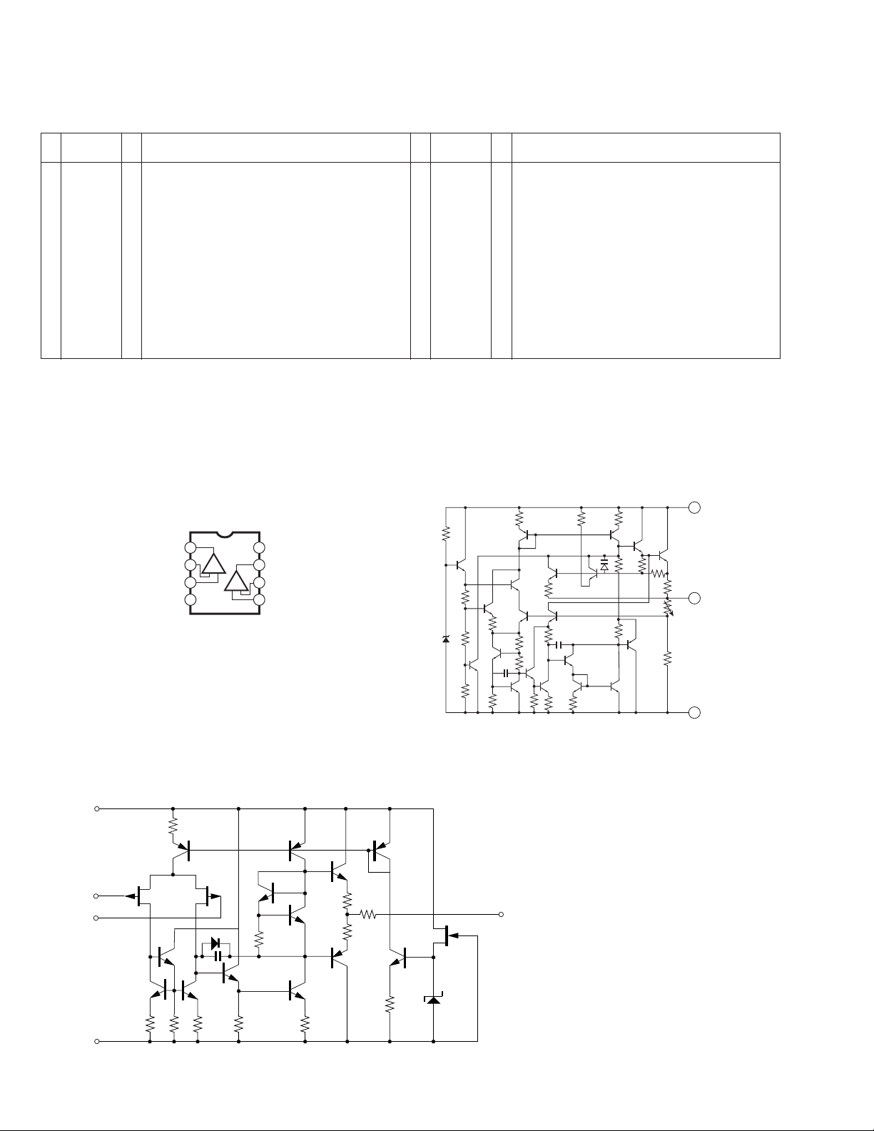
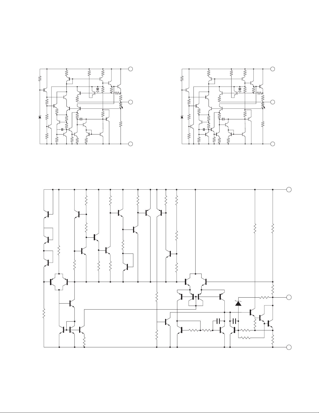
■ IC BLOCK DIAGRAM (ICブロック図)
• NJM2068M-D (TE2) (X3505A00)
Dual Operational Amplifier
JACK20: IC702, 752, 802, 852
MIX20: IC001, 003, 901, 902, 951, 952, ICM01
USB: IC103, 104
+-
+V
+DC Voltage
8
Supply
7
Output B
Inverting
6
Input B
Non-Inverting
5
Input B
Output A
Inverting
Input A
Non-Inverting
Input A
-DC Voltage Supply
1
2
+-
3
4
-V
• NJM072BM-E (TE1) (X4543A00)
Dual Operational Amplifier
JACK20: IC101, 201, 301, 401, 501, 601
+
V
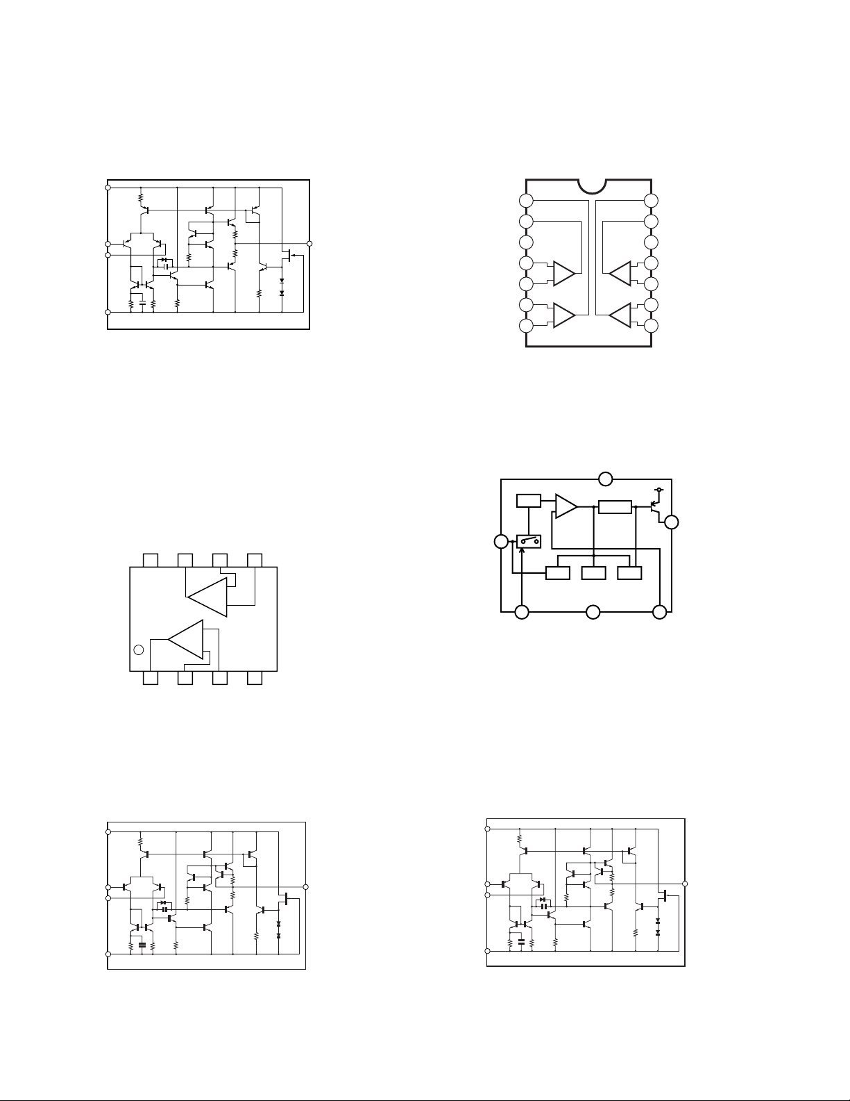
• KIA7812API (X4153A00)
Regulator +12V
PS20: IC105
R22 R23R17
R1
Q12
R12
R11
Z1
R13
Q13
Q18
Q2
Q11
Q17
Q1
R18
R2
R3
Q3Q4Q5 Q9
R4
R5
Q14
R19
Q6
C1
Q7
R6R7R8
Q19
Q11-1
R10R9R15
Q8
Q10
Q15
Q16
R14
R16
R20
R21
1
3
2
INPUT
OUTPUT
COMMON (GND)
24
-
INPUT
+
INPUT
OUTPUT
-
V
MG206C-USB/MG206C
• KIA7805API/P (X4928A00)
Regulator +5V
PS20: IC107
R22 R23R17
R1
Q12
R12
R11
Z1
R13
Q13
Q18
R18
Q2
R4
Q11
Q14
Q17
R19
Q1
R2
R3
Q3Q4Q5 Q9
R5
Q19
Q6
C1
Q7
R6R7R8
• KIA7915PI (X4931A00)
Regulator -15V
PS20: IC102, 104
R
15
Q
28
Q
29
Q
30
Q
17
R
16
R
1
R
14
Q
18
R17R
Q
Q11-1
Q8
R
19
R10R9R15
Q10
18
Q
19
Q15
20
• KIA7815API (X4930A00)
Regulator +15V
PS20: IC101, 103
1
INPUT
R1
Q16
R14
R16
3
OUTPUT
R20
R21
2
COMMON (GND)
R
Q
21
Q
23
R
20
Q
31
R
21
22
Q
22
Q
24
Q
25
R12
R11
Z1
R13
R
23
R
24
R
25
Q12
Q2
Q13
R22 R23R17
Q11
Q14
Q17
R19
Q18
Q1
R18
R2
R3
Q3Q4Q5 Q9
R4
R5
Q6
C1
Q7
R6R7R8
Q19
Q11-1
R10R9R15
Q8
Q15
Q10
1
INPUT
Q16
R14
R16
3
OUTPUT
R20
R21
2
COMMON (GND)
GND
(1)
R
13
R
12
Q
Q
13
Q2Q
3
R
26
Q
R
0
Q
4
7
Q
5
Q
6
R
2
Q
26
Q
8
Q
R
3
12
R
Q
26-1
Q
27-1
R
R
9
4
Q
27
C
2
5
Q
10
D
4
C
1
R
9
R
6
R
7
Q
11
11
R
10
Q
14
Q
15
R
8
OUTPUT
(3)
Q
16
INPUT
(2)
25
MG206C-USB/MG206C
• NJM4580M-D (TE2) (X5025A00)
Dual Operational Amplifier
JACK20: IC001, 002, 701, 801
V+
8
–INPUT
+INPUT
2, 6
3, 5
V–
4
1, 7
• BA4560RF-E2 (X6897A00)
Dual Operational Amplifier
JACK20: IC102, 103, 153, 202, 203, 253, 302, 303, 353
IC402, 403, 453, 502, 602, 703, 803, 901-903
MIX20: IC002, 004, 101, 102, 151, 201, 202, 251
IC301, 302, 351, 401, 402, 451, 501, 502, 551
IC601, 602, 651, 701, 702, 751, 752, 801, 802
IC851, 852, 903-905, ICM03
V
CC
OUT2 + IN2- IN2
8765
–
Ch2
+
+
Ch1
–
OUTPUT
• BA10339F (X6266A00)
Comparator
MIX20: ICM06-11
1
OUT2
2
OUT1
3
Vcc
4
–IN1
+IN1
–IN2
+IN2
–
+
5
6
–
+
7
• BA00CC0WFP-E2 (X7256A00)
Regulator 3V to 15V
USB: IC102
V
ref
+-
V
CC
2
OVP
TSD OCP
15
CTL GND
FIN
3
Driver
N.C.
14
OUT3
OUT4
13
12
GND
+IN4
11
+
–
10
–IN4
9
+IN3
+
–
8
–IN3
V
OUT
4
C
1234
OUT1 + IN1- IN1 V
• NJM4565M (TE1) (X7378A00)
Dual Operational Amplifier
JACK20: IC104, 204, 304, 404
MIX20: ICM02, 05
V+
8
2, 6
–INPUT
+INPUT
3, 5
V–
4
26
EE
• NJM4556AL (XP844A00)
Dual Operational Amplifier
MIX20: ICM04
V+
8
1, 7
OUTPUT
–INPUT
+INPUT
2, 6
3, 5
V–
4
1, 7
OUTPUT

MG206C-USB MG206C
■ CIRCUIT BOARDS (シート基板図)
CONTENTS (目次)
• JACK20F Circuit Board (X8284C0) ........................................... 28
• JACK20R Circuit Board (X8284C0) ........................................... 27
• MIX20 Circuit Board (X8283C0) ........................................... 32
• PS20 Circuit Board (X8285C0) ........................................... 36
• USB Circuit Board (X7196C0) ........................................... 27
Note: See parts list for details of circuit board component parts.
注:シートの部品詳細はパーツリストをご参照ください。
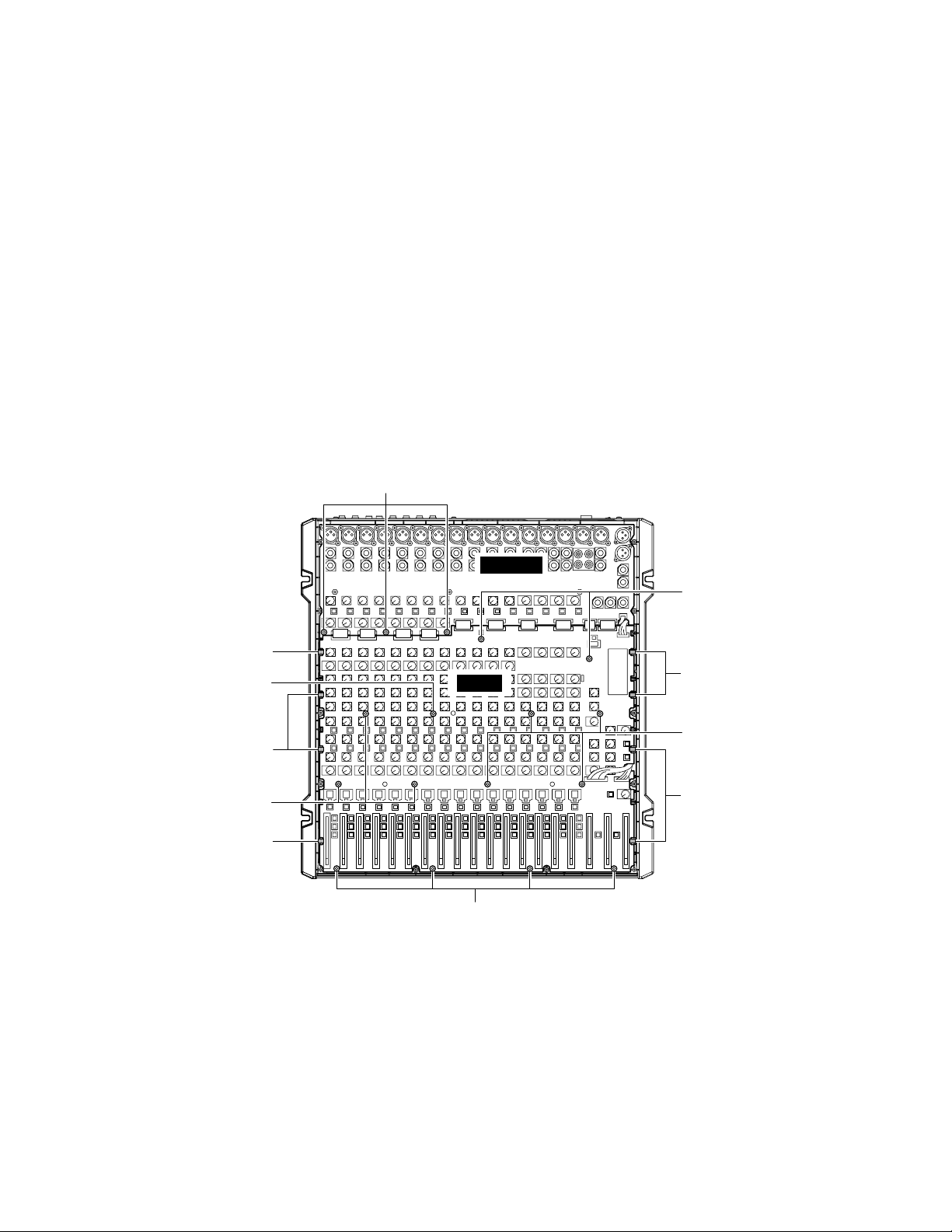
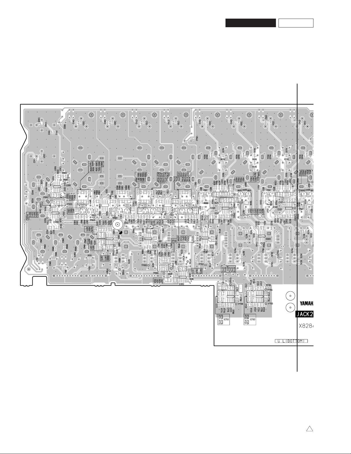
• JACK20R Circuit Board
MG206C-USB/MG206C
to MIX20 CN004 to PS20 CN103 to USB CN101 to MIX20 CN003
• USB Circuit Board (MG206C-USB only)
USB
Component side (部品側)
Pattern side (パターン側)
2NA-WJ26400
1
to JACK20R CN903
Component side (部品側)
Pattern side (パターン側)
2NA-WG33610
27

MG206C-USB/MG206C
M
• JACK20F Circuit Board
Reduction: 4/5
MG206C-USB MG206C
A
28
to MIX20 CN101 to MIX20 CN201 to MIX20 CN301 to MIX20 CN401 to MIX20 CN501 to
A'
Component side (部品側)
2NA-WJ26400
1
MG206C-USB MG206C
A
MG206C-USB/MG206C
Reduction: 3/5
to MIX20 CN601
A'
2NA-WJ26400
to MIX20 CN701 to MIX20 CN801 to MIX20 CN002
to MIX20 CN001
to PS20 CN102
Component side (部品側)
1
29
MG206C-USB/MG206C
• JACK20F Circuit Board
Reduction: 4/5
MG206C-USB MG206C
B
30
Pattern side (パターン側)
B'
2NA-WJ26400
1
 Loading...