

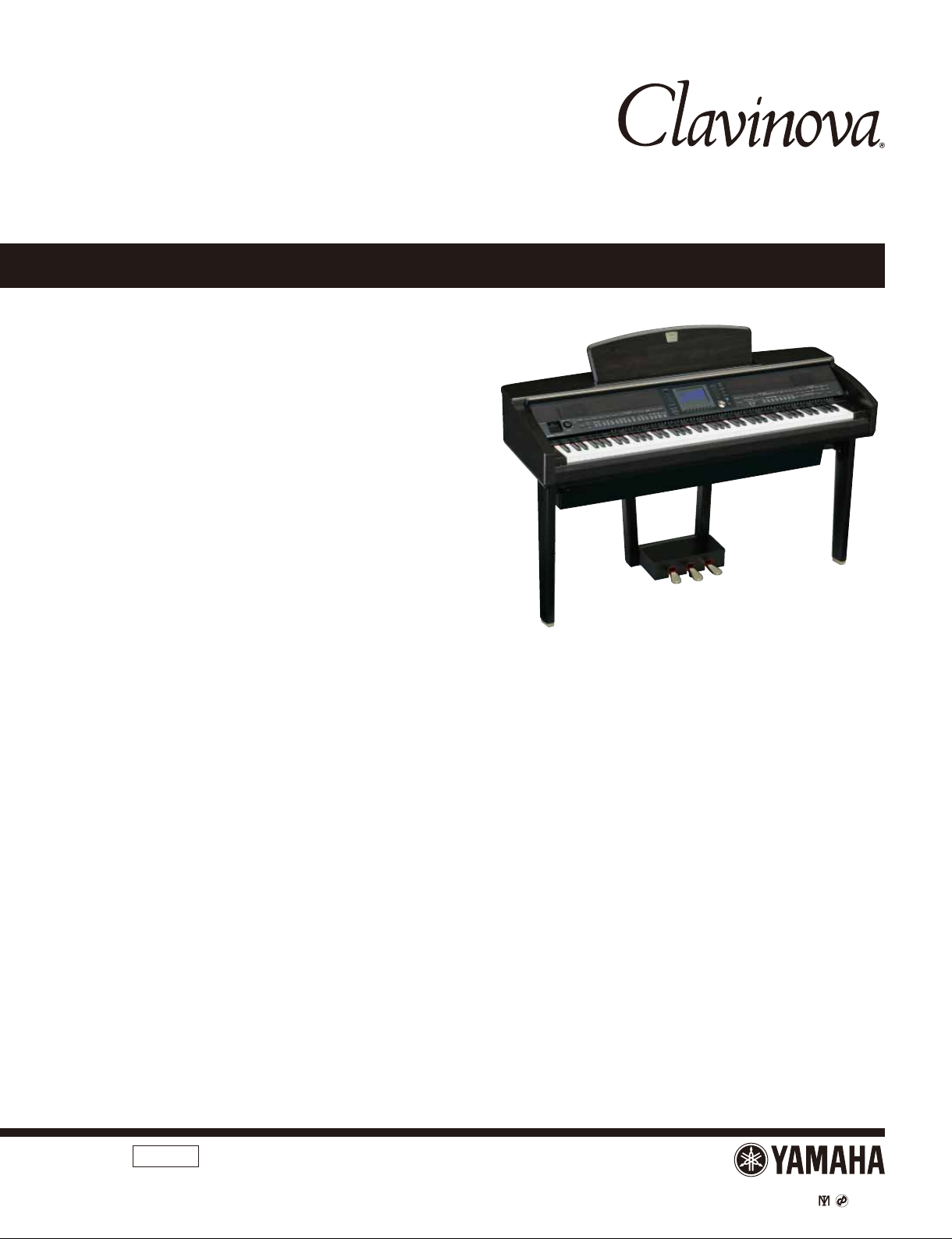
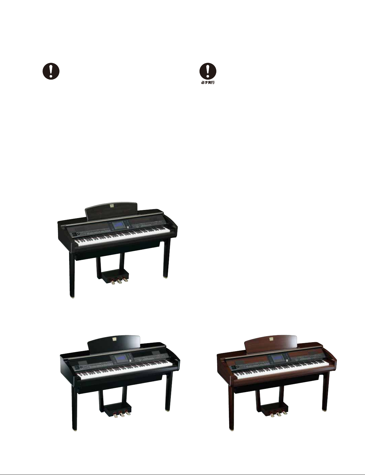
CVP-405/ CVP-405PE/ CVP-405PM
SERVICE MANUAL
CVP-405
CONTENTS
■
SPECIFICATIONS
PANEL LAYOUT
DISASSEMBLY PROCEDURE
LSI PIN DESCRIPTION
IC BLOCK DIAGRAM
CIRCUIT BOARDS
TEST PROGRAM
FACTORY SET
DATA BACKUP
VERSION UPGRADE
CHANGING THE DISPLAY LANGUAGE
(画面に表示される言語を切り替える)
SYSTEM BOOTING FLOWCHART
(起動フローチャート)
MIDI IMPLEMENTATION CHART ...................................................102
MIDI DATA FORMAT .......................................................................103
PARTS LIST
BLOCK DIAGRAM
CIRCUIT BOARD LAYOUT & WIRING
(ユニットレイアウト&結線図)
OVERALL CIRCUIT DIAGRAM
(目次)
(総合仕様)
(パネルレイアウト)
(LSI 端子機能表)
(IC ブロック図)
(シート基板図)
(テストプログラム)
(出荷時の設定)
(データのバックアップ)
(バージョンアップ)
.................................................................98/100
(ブロックダイアグラム)
..........................................................4/6
................................................8
(分解手順)
.............................................43
..................................................47
........................................69/77
...................................................76/84
..............................................97
(総回路図)
.......................................12
........................................35
....................................85/88
..................................91/94
001788
CL
CVP-405: 20070710-451500
CVP-405PE: 20070710-504000
CVP-405PM: 20070710-535500
Copyright (c) Yamaha Corporation. All rights reserved. PDF ’07.07
HAMAMATSU, JAPAN
CVP-405/CVP-405PE/CVP-405PM
IMPORTANT NOTICE
This manual has been provided for the use of authorized Yamaha Retailers and their service personnel. It has been
assumed that basic service procedures inherent to the industry, and more specifi cally Yamaha Products, are already
known and understood by the users, and have therefore not been restated.
WARNING :
personal injury, destruction of expensive components and failure of the product to perform as
specifi ed. For these reasons, we advise all Yamaha product owners that all service required should
be performed by an authorized Yamaha Retailer or the appointed service representative.
IMPORTANT :
certification, recognition of any applicable technical capabilities, or establish a principal-agent
relationship of any form.
The data provided is believed to be accurate and applicable to the unit (s) indicated on the cover. The research
engineering, and service departments of Yamaha are continually striving to improve Yamaha products. Modifi cations are,
therefore, inevitable and changes in specifi cation are subject to change without notice or obligation to retrofi t. Should any
discrepancy appear to exist, please contact the distributor’s Service Division.
WARNING :
may have accumulated by grounding yourself to the ground bus in the unit (heavy gauge black wires
connect to this bus).
IMPORTANT :
power to the unit.
Failure to follow appropriate service and safety procedures when servicing this product may result in
This presentation or sale of this manual to any individual or fi rm does not constitute authorization,
Static discharges can destroy expensive components. Discharge any static electricity your body
Turn the unit OFF during disassembly and parts replacement. Recheck all work before you apply
WARNING : CHEMICAL CONTENT NOTICE !
The solder used in the production of this product contains LEAD. In addition, other electrical/electronic and/or plastic
(where applicable) components may also contain traces of chemicals found by the California Health and Welfare Agency
(and possibly other entities) to cause cancer and/or birth defects or other reproductive harm.
DO NOT PLACE SOLDER, ELECTRICAL/ELECTRONIC OR PLASTIC COMPONENTS IN YOUR MOUTH FOR ANY
REASON WHAT SO EVER!
Avoid prolonged, unprotected contact between solder and your skin! When soldering, do not inhale solder fumes or
expose eyes to solder/fl ux vapor!
If you come in contact with solder or components located inside the enclosure of this product, wash your hands before
handling food.
IMPORTANT NOTICE FOR THE UNITED KINGDOM
Connecting the Plug and Cord
IMPORTANT .
BLUE: NEUTRAL
BROWN: LIVE
As the colours of the wires in the mains lead of this apparatus may not correspond with the coloured markings identifying
the terminals in your plug proceed as follows:
The wire which is coloured BLUE must be connected to the terminal which is marked with the letter N or coloured BLACK.
The wire which is coloured BROWN must be connected to the terminal which is marked with the letter L or coloured RED.
Making sure that neither core is connected to the earth terminal of the three pin plug.
The wires in this mains lead are coloured in accordance with the following code:
WARNING
■
Components having special characteristics are marked and must be replaced with parts having specifi cation equal
to those originally installed.
印の部品は、安全を維持するために重要な部品です。交換する場合は、安全のために必ず指定の部品をご使用ください。
2
SAVING DATA
■
■
データの保存
CVP-405/CVP-405PE/CVP-405PM
Saving and backing up your data
The data of the types listed below are lost when you
turn off the power to the instrument. Save the data
Be sure to
perform it
•
to the USER tab display, USB storage device (USB
fl ash memory/fl oppy disk, etc).
• Recorded/Edited Songs
• Created/Edited Styles
• Edited Voices
• Memorized One Touch Settings
• Edited MIDI settings
Moreover, the above-mentioned data can be saved
all at once. Data in the USER tab display may be
lost due to malfunction or incorrect operation. Save
important data to a USB storage device (USB fl ash
memory/fl oppy disk, etc). (For the details, refer to
page 85.)
CVP-405
作成したデータの保存とバックアップ
下記のデータは、保存前に電源を切ると消えてしま
います。
保存しておきたいデータは「ユーザー」画面や、
USB 記憶装置(USB フラッシュメモリー / フロッピー
ディスク な ど ) に保 存 してくだ さ い 。
・録音 / 編 集したソング
・スタイル 制 作 で 制 作 / 編 集した スタイル
・ボイス 編 集 で 編 集した ボ イス
・設定を 登 録したワンタッチセッティング
・MI DI 設定 編 集で編 集した MI DI 設定
また、上記 データは一括で 保存することができます。
「ユーザー」画面に保存したデータは故障や誤操作
などのために失われ ることがあります。 大 切なデー
タは、USB記憶装置(USBフラッシュメモリー / フ
ロッピーディスクなど ) に 保 存してください 。(詳細は、
88 ページを参照してください。)
CVP-405PE
•
CVP-405PM
•
3
CVP-405/CVP-405PE/CVP-405PM
SPECIFICATIONS
■
Ke draobyeK)3HG(3remmaHdedarGdraoby
Number of keys 88
Display
Wallpaper Customize
(Lyrics display)
P 821)xam(ynohpylo
Voice Selection
S. Articulation!
Voice
Effects
Accompaniment Style
Effect
Blocks
Effect
Types
V resU01+teserP06ynomraHlaco
Fingering
OTS
(One Touch Setting)
O SEYkniLST
Music
Finder
Voice
Reverb/Chorus/
DSP/Master
Reverb/Chorus/
DSP
Part straP72QE
gnilpmaSoeretScimanyDMWAecruoSdnuoS
320
240 dots QVGA
color 5.7 inch LCD
SEYsciryL,erocScisuM
SEY
414 voices + 480 XG
19 Drum/SFX Kits + GM2
ecioV!eviL
!setulFnagrO
Reverb: 34 Preset + 3 User
Chorus: 29 Preset + 3 User
DSP 1: 191 Preset + 3 User
DSP 2–4: 106 Preset + 10 User
retsaM
Single Finger, Fingered, Fingered On Bass, Multi Finger, AI Fingered, Full Keyboard,
Voices
+ GS (GS Voices for GS
Song playback)
12ecioV!larutaN
42
51ecioVageM
02
62ecioV!looC
22ecioV!teewS
01
672ecioVralugeR
SEYrotaerCdnuoS
6
1enohporciM
resU2+teserP5QE
443selytStneminapmoccA
482selytSorP
42selytSnoisseS
63selytStsinaiP
SEYselytSecioVageM
AI Full Keyboard
SEYrotaerCelytS
4 for Each Style
SEYteserP
SEYtidE
4
CVP-405/CVP-405PE/CVP-405PM
021sgnoSteserP
EMITeuClacoV,yeK-oaraK,yeKynA,sthgiLwolloFediuG
Song
Internet Direct Connection
Memory
Device
Tempo
Registration Memory
Others
USB
Connection
Other Connectors
Pedals Functions
Amplifiers/
Speakers
Dimensions [W D H]
(with the Music Rest)
W )zo8/52,.sbl471(gk97thgie
Optional
Accessories
Accessories
Performance assistant technology
Memory Card (SmartMedia, etc.)
T opmeTpaT,005–5egnaRopme
Language for Display 6 Languages (English, Japanese, German, French, Spanish, Italian)
Piano Reset Button
(incl. Piano Lock)
Tr retsaM/gnoS/draobyeKesopsna
USB to HOST
(Computer)
USB TO DEVICE
(left side of front panel)
USB TO DEVICE (bottom left
panel of the instrument)
F 5CF/4CFhctiwStoo
F 7CFrellortnoCtoo
SEYpmaLediuG
YES
S,gnidroceRitluM,gnidroceRkciuQgnidroceR
61slennahCdroceR
SEYredroceRoiduABSU
LAN Port, Wireless Game Adaptor (LAN Port),
External adaptor (via USB to DEVICE)
SEYyromeMhsalFBSU
)ECIVEDotBSUaiv(rotpadalanretxE)DD2,DH2(ksiDyppolF
)ECIVEDotBSUaiv(rotpadalanretxEksiDdraH
BM4.1tuoba)lanretnI(yromeMhsalF
External adaptor (via USB to DEVICE)
SEYemonorteM
)segaugnaL5(secioVnamuH,ffo/nolleBdnuoS
8snottuB
SEYezeerF/ecneuqeS.tsigeR
SEYomeD
SEYsseccAtceriD
YES
9epyTelacS
YES
YES
SEY
PHONES 2, MIDI (THRU, OUT, IN), AUX PEDAL, AUX IN (L/L+R, R),
AUX OUT (L/L+R, R), LAN
MIC (INPUT VOLUME,
MIC./LINE IN),
VIDEO OUT
VOLUME, SUSTAIN, SOSTENUTO, SOFT, GLIDE, S. Articulation,
SONG PLAY/PAUSE, STYLE START/STOP, etc.
W04+W04srefiilpmA
mc5+mc61srekaepS
1430 mm 609 mm 890 mm
[56 1/2" 24" 35 1/8"]
(1430 mm 609 mm 1047 mm)
[56 1/2" 24" 41 3/8"]
061-EPHsenohpdaeH
10DF-DUtinUDDF-BSU
Guide to Yamaha Online Member Product User Registration
"50 greats for the Piano" Music Book, Owner's Manual, Data List
The following items may be included or optional,
depending on your locale:
Bench
gnitidEgnoS,gnidroceRpet
5
CVP-405/CVP-405PE/CVP-405PM
総合仕様■
音源 AWMダイナミックステレオサンプリン
鍵盤
鍵盤数
ディスプレイ
譜面表示、歌詞表示 ○
歌詞画面背景カスタマイズ ○
最大同時発音数 821
内蔵ボイス数
ナチュラルボイス 12
スーパーアーティ
キュレーション
ボイス
エフェクト
スタイル
ソング
ボイス編集 ○
エフェクト
ブロック
エフェクト
タイプ
ボーカルハーモニー 60プリセット + 10 ユーザー
内蔵スタイル数 443
メガボイススタイル ○
フィンガリング
スタイルクリエーター ○
OTS(ワンタッチセッティング) 各スタイルに 4種類
OTSリンク ○
ミュージッ
クファイン
ダー
内蔵ソング数 221
ガイド
パフォーマンスアシスタント ○
録音 クイック録音、多重録音、ステップ録音、ソング編集
ボイス
メガボイス 51
ライブボイス 02
クールボイス 62
スイートボイス 22
オルガンフルート 01
レギュラーボイス 672
リバーブ /コーラ
ス/DSP
マイク 1
リバーブ /
コーラス /DSP
マスター
イコライザー
パート
イコライザー
プロ 482
セッション 42
ピアニスト 63
プリセット ○
エディット ○
ガイドランプ ○
録音チャンネル数 16
グレードハンマー3(GH3)鍵盤
88
320×240ドット
QVGAカラー
5.7インチ LCD
414ボイス + 480 XGボイス
19ドラム/SFXキット+GM2
+ GS (GSソング再生用)
24
6
リバーブ : 34 プリセット + 3ユーザー
コーラス : 29 プリセット + 3ユーザー
DSP 1: 191 プリセット + 3ユ ーザー
DSP 2-4: 106 プリセット + 10 ユーザー
5プリセット + 2 ユーザー
27パート
シングルフィンガー、フィンガード、フィンガードオンベース、
マルチフィンガー、AI フィンガード、フルキーボード、AIフルキーボード
フォローライツ、エニーキー、カラオキー、
ボーカルキュータイム
6
USB オーディオレコーダー ○
インターネットダイレクト接続
USBフラッシュメモリー 接続可
フロッピーディスク(2HD,
記憶媒体
デバイス
テンポ
レジスト
レーション
メモリー
その他
USB接続
付属端子
ペダルに割り当てられる機能
アンプ出力/
スピーカー
定格電源 AC100V 50/60 Hz
消費電力 W56
寸法[間 口×奥行×高さ]
( ) 内は譜面立てを立てた場合
質量 gk97
別売品
付属品
2DD)
ハードディスク USBタイプハードディスク接続可 (USB TO DEVICE端子使用 )
フラッシュメモリー(内蔵 ) BM4.1約
メモリーカード
(スマートメディアなど)
テンポ範囲 5〜500、タップ
メトロノーム ○
サウンド ベルオン /オフ、ヒューマンボイス(5言語)
ボタン 8
レジストレーションシーケンス
/フリーズ
デモ ○
ディスプレイに表示される言語 6言語(日、英、独、仏、西、伊)
ダイレクトアクセス ○
ピアノリセットボタン
(ピアノロック含む)
トランスポーズ キーボード、ソング、マスター
スケール 9
USB TO HOST
(コンピューター接続)
USB TO DEVICE
(トップパネル左側)
USB TO DEVICE
(本体底面端子パネル )
アンプ出力 W04+W04
スピーカー mc5+mc61
ヘッドフォン HPE-160
フットスイッチ FC 4/FC 5
フットコントローラー FC 7
USB-FDD ユニット
LAN端子使用、無線LANイーサネットコンバーター(LAN端子使用)、
USB-LANアダプター(USB TO DEVICE端子使用 )
USBタイプフロッピーディスクドライブ接続可
(USB TO DEVICE端子使用 )
USBタイプメモリーカードリーダー接続可
(USB TO DEVICE端子使用 )
○
○
○
○
○
PHONES端子×2、MIDI (THRU, OUT, IN)端子、AUX PEDAL 端子、
AUX IN (L/L+R, R) 端子、AUX OUT (L/L+R, R)端子、LAN端子
マイク端子(INPUT VOLUME, MIC./LINE IN)
VIDEO OUT 端子
ボリューム、サステイン、ソステヌート、ソフト、グライド、
スーパーアーティキュレーションボイス、
ソングスタート/一時停止、スタイルスタート/ストップ、その他
1430 mm × 609 mm ×890 mm
(1430 mm× 609 mm ×1047 mm)
UD-FD01
保証書、ヤマハオンラインメンバー製品ユーザー登録のご案内、取扱説明書、
取扱説明書別冊「クイックガイド」、取扱説明書別冊「データリスト」、
ヘッドフォン、イス(高さ調節付き)
CVP-405/CVP-405PE/CVP-405PM
7
CVP-405/CVP-405PE/CVP-405PM
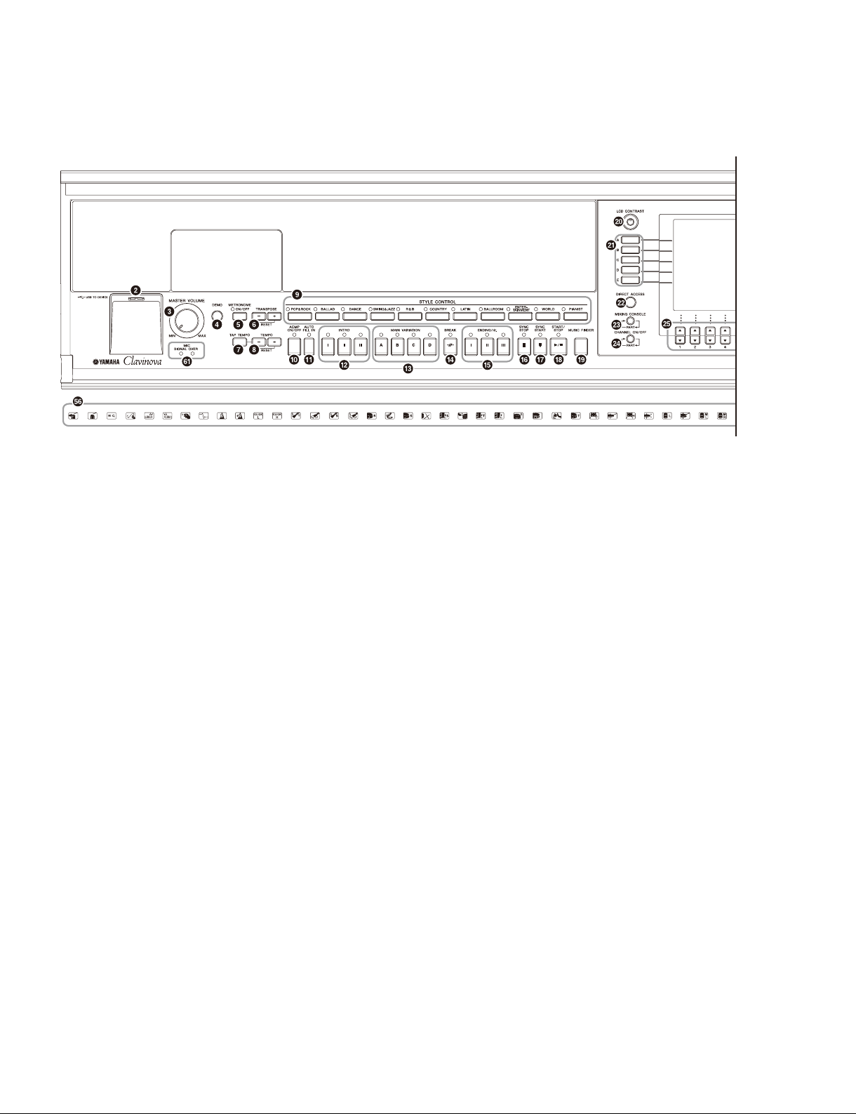
PANEL LAYOUT
(パネルレイアウト)■
※掲載したパネル図は海外用です。(英語表記)
国内用パネルは、日本語表記となります。
A
A'
[POWER] switch
q
[USB TO DEVICE] Terminal
w
[MASTER VOLUME] dial
e
[DEMO] button
r
METRONOME
[ON/OFF] button
t
TRANSPOSE
-
] [ + ] buttons
[
y
TEMPO
[TAP TEMPO] button
u
-
] [ + ] buttons
[
i
STYLE CONTROL
STYLE category selection buttons
o
[ACMP ON / OFF] button
!0
[AUTO FILL IN] button
!1
INTRO [Ι] / [ΙΙ] / [
!2
MAIN VARIATION [A] / [B] / [C] / [D] buttons
!3
[BREAK] button
!4
ENDING/rit. [Ι] / [ΙΙ] / [
!5
[SYNC STOP] button
!6
[SYNC START] button
!7
[START/STOP] button
!8
[MUSIC FINDER] button
!9
[LCD CONTRAST] knob
@0
[A]–[J] buttons
@1
] buttons
ΙΙΙ
] buttons
ΙΙΙ
8
q 電源
w [USBTODEVICE]
(ユーエスビートゥーデバイス)端子
e [ 音量 ]
r [ デモ ]
メトロノーム
t[オン/オフ]
トランスポーズ
-
][+]
y[
テンポ
u [ タップ ]
i[
-
][+]
スタイルコントロール
o スタイルボタン
!0[ スタイルオン / オフ ]
!1 [ フィルインオン / オフ ]
!2 イントロ [Ι]/[ΙΙ ]/[ΙΙΙ]
!3メイン [A]/[B]/[C]/[D]
!4[ ブレイク ]
!5エンディング /rit.[Ι]/[ΙΙ]/[ΙΙΙ ]
!6[ シンクロストップ ]
!7 [ シンクロスタート ]
!8 [ スタート / ストップ ]
!9 [ ミュージックファインダー ]
@0 [ 画面コントラスト ]
@1 [A] 〜 [J]
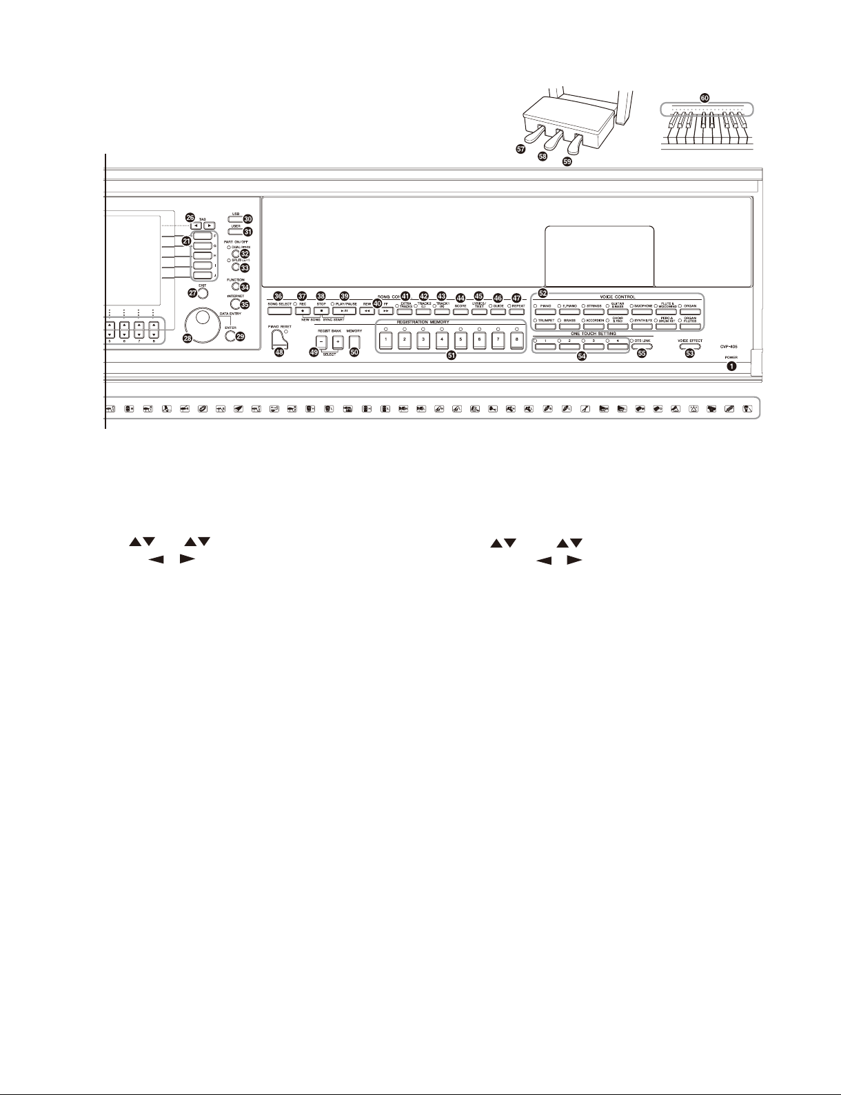
CVP-405/CVP-405PE/CVP-405PM
A
A'
[DIRECT ACCESS] button
@2
[MIXING CONSOLE] button
@3
[CHANNEL ON/OFF] button
@4
[1
@5
TAB [
@6
[EXIT] button
@7
[DATA ENTRY] dial
@8
[ENTER] button
@9
[USB] button
#0
[USER] button
#1
PART ON/OFF
[DUAL (RIGHT2)] button
#2
[SPLIT (LEFT)] button
#3
[FUNCTION] button
#4
[INTERNET] button
#5
SONG CONTROL
[SONG SELECT] button
#6
[REC] button
#7
[STOP] button
#8
[PLAY / PAUSE] button
#9
[REW] / [FF] buttons
$0
[EXTRA TRACKS] button
$1
[TRACK 2 (L)] button
$2
[TRACK 1 (R)] button
$3
[SCORE] button
$4
[LYRICS/TEXT] button
$5
[GUIDE] button
$6
[REPEAT] button
$7
]–[8
][
] buttons
] buttons
@2 [ ダイレクトアクセス ]
@3 [ ミキサー ]
@4 [ チャンネルオン / オフ ]
@5[1
@6 タブ切替 [
@7 [ 戻る ]
@8 [ データダイアル ]
@9 [ エンター ]
#0[USB](ユーエスビー)
#1 [ ユーザー ]
鍵盤パート オン / オフ
#2 [ デュアル ( 右手 2)]
#3 [ スプリット ( 左手 )]
#4 [ ファンクション ]
#5 [ インターネット ]
ソングコントロール
#6[ ソング選択 ]
#7[ 録音 ]
#8[ ストップ ]
#9[ スタート / 一時停止 ]
$0[ 巻き戻し ]/[ 早送り ]
$1[ その他トラック ( スタイル )]
$2[ トラック 2( 左手 )]
$3[ トラック 1( 右手 )]
$4[譜面]
$5[ 歌詞 / テキスト ]
$6 [ ガイド ]
$7[ くり返し ]
]〜[8 ]
][ ]
9

CVP-405/CVP-405PE/CVP-405PM
PIANO Setting
[PIANO RESET] button
$8
REGISTRATION MEMORY
REGIST BANK [+] [–] buttons
$9
[MEMORY] button
%0
[1]–[8] buttons
%1
VOICE CONTROL
VOICE category selection buttons
%2
[VOICE EFFECT] button
%3
ONE TOUCH SETTING
[1]–[4] buttons
%4
[OTS LINK] button
%5
Drum Kit icons
%6
Pedals
Left pedal
%7
Sostenuto pedal
%8
Damper pedal
%9
ピアノ設定
$8 [ ピアノリセット ]
レジストレーションメモリー
$9 レジストレーションバンク [-][+]
%0 [ メモリー ]
%1 [1] 〜 [8]
ボイスコントロール
%2 ボイスボタン
%3 [ ボイスエフェクト ]
ワンタッチセッティング (OTS)
%4 [1] 〜 [4]
%5 [OTS リンク ]
%6 ドラムキットアイコン
ペダル
%7 レフトペダル
%8 ソステヌートペダル
%9 ダンパーペダル
Keyboard guide lamps
^0
Mic signal/over lamps
^1
^0 鍵盤ガイドランプ
^1 マイクシグナル / オーバーランプ
10
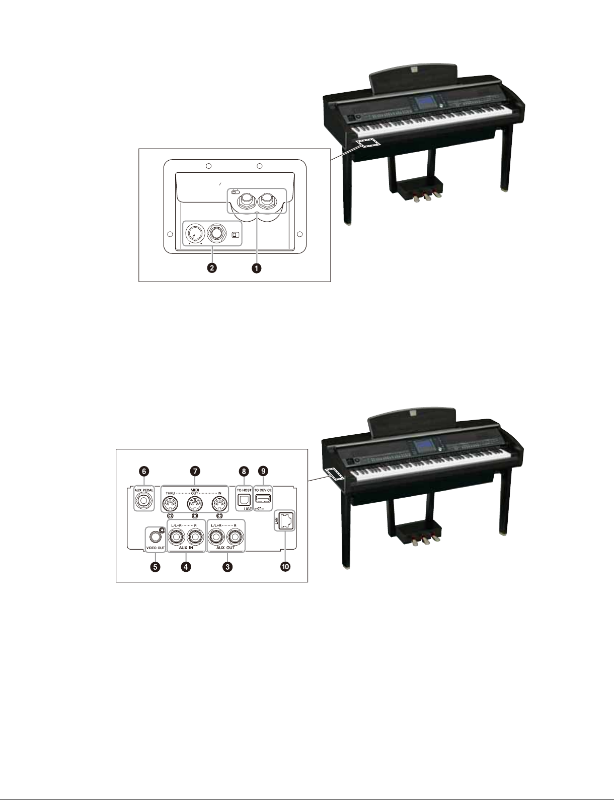
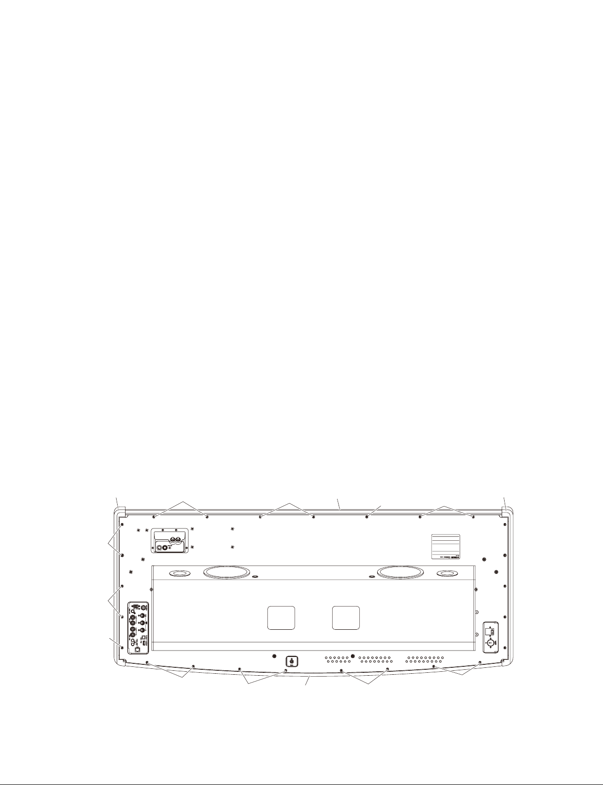
INPUT
VOLUME
MIN MAX
MIC.
LINE IN
CVP-405/CVP-405PE/CVP-405PM
MIC. LINE PHONES
[PHONES] jacks
q
• [MIC./LINE IN] jack
w
• [INPUT VOLUME] dial
q [PHONES](フォーンズ)端子
• [MIC.
w
• [INPUT VOLUME]
/LINEIN](マイク/ラインイン)端子
(インプットボリューム)ダイアル
[AUX OUT] jacks
e
[AUX IN] jacks
r
[VIDEO OUT] terminal
t
[AUX PEDAL] jack
y
[MIDI] terminals
u
[USB TO HOST] terminal
i
[USB TO DEVICE] terminal
o
[LAN] port
!0
e [AUXOUT](エーユーエックスアウト)端子
r [AUXIN](エーユーエックスイン)端子
t [VIDEOOUT](ビデオアウト)端子
y [AUXPEDAL](エーユーエックスペダル)端子
u [MIDI](ミディ)端子
i [USBTOHOST](ユーエスビートゥーホスト)端子
o [USBTODEVICE]
(ユーエスビートゥーデバイス)端子
!0 [LAN](ラン)端子
11
CVP-405/CVP-405PE/CVP-405PM
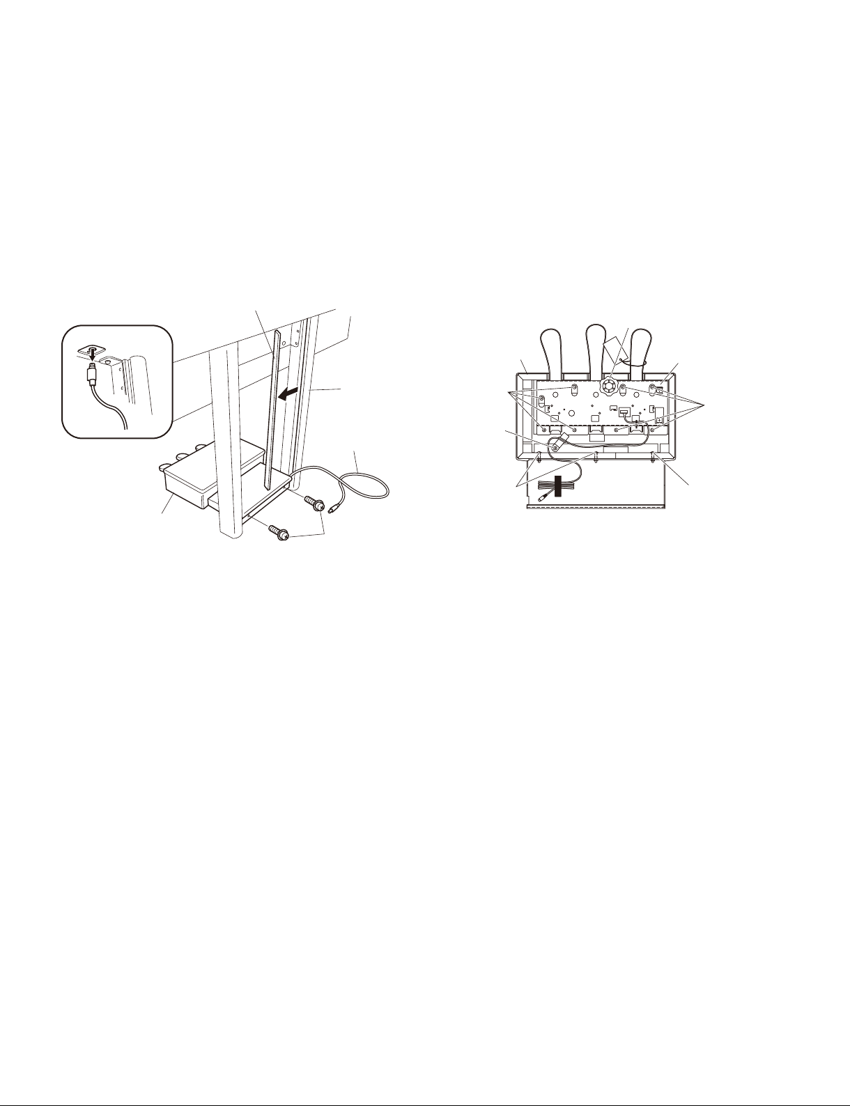
DISASSEMBLY PROCEDURE
(分解手順)■
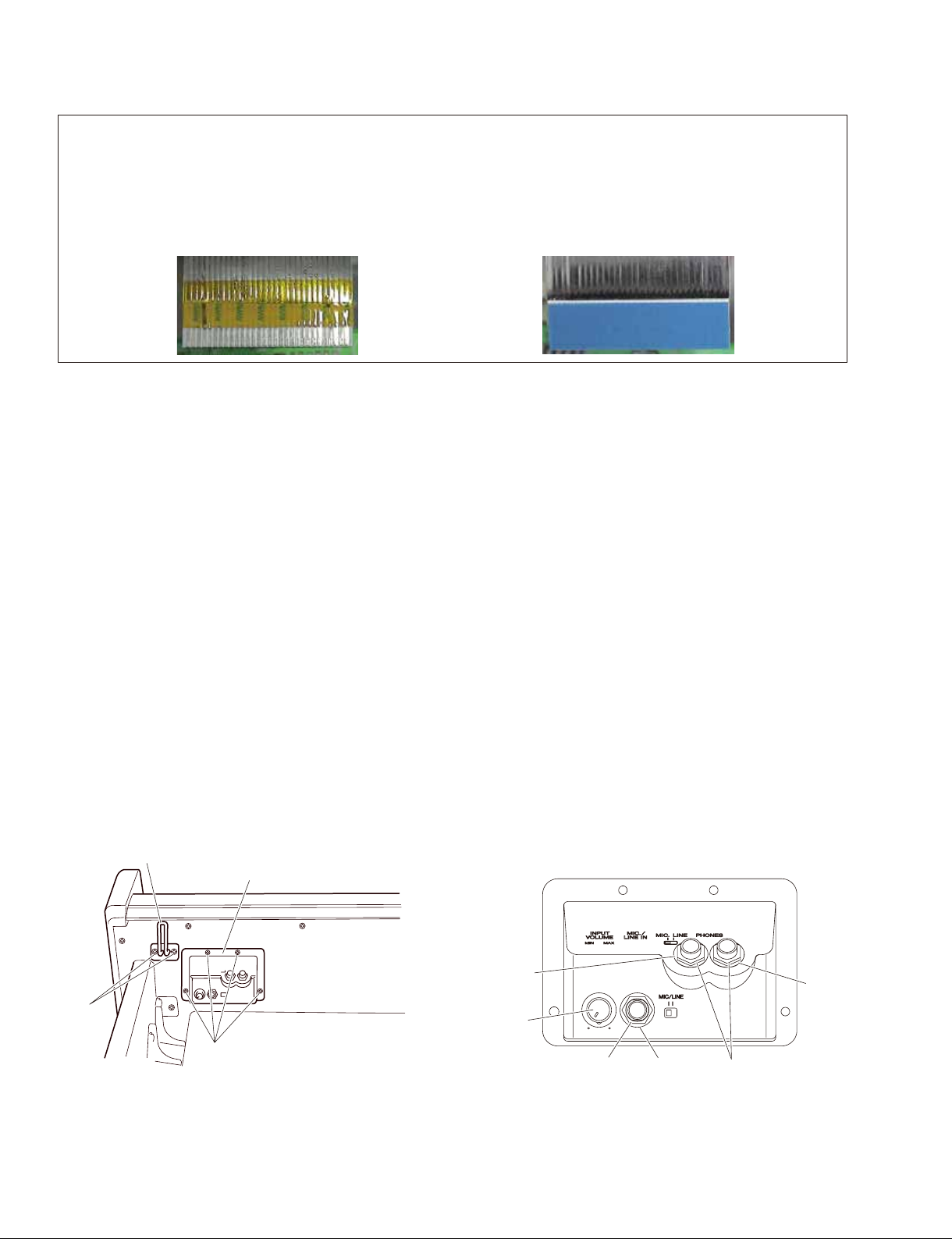
Caution:
1. Be sure to attach the removed fi lament tape just as it
was before removal.
2. Pay attention not to insert and install the cable to the
connector inversely. (Fig. A)
Front Side (Printed Side)
(表面(印刷面))
1. Headphone Hanger
(Time required : About 1 minute)
Remove the two (2) screws marked [17b]. The
headphone hanger can then be removed. (Fig. 1)
2.
Mic. & Phones Unit, MIC and HP Circuit
(Time required : About 3 minutes each)
Boards
2-1. Remove the four (4) screws marked [77]. The mic. &
phones unit can then be removed. (Fig. 1)
2-2.
MIC Circuit Board
2-2-1. Remove the input volume knob, the hexagonal nut
marked [N1] and the washer marked [W1]. (Fig. 2-2)
2-2-2. Remove the hexagonal nut marked [40A] and the
washer marked [50A]. The MIC circuit board can
then be removed. (Fig. 2-1)
* When installing the INPUT VOLUME knob, set it to the
VOL. MIN position, that is, align the bar on the knob
with the point on the case as shown in the fi gure. (Fig.
2-1)
2-3.
HP Circuit Board
Remove the two (2) hexagonal nuts marked [40B] and
the two (2) washers marked [50B]. The HP circuit
board can then be removed. (Fig. 2-1)
注意事項
1. フィラメントテープは、取り外す前と同じように取り付けてく
ださい。
2. フラットケーブルの表・裏を逆に差し込まないように注意し
て取り付けてください。(図 A)
Back Side
(Fig.A)(図 A)
(裏面)
1. ヘッドホンハンガー(所要時間:約 1 分)
[17b]のネジ2本を外し、ヘッドホンハンガーを外しま
す。(図 1)
2. MIC-HPJ ユニット、MIC シート、HP シー
(所要時間:各約 3 分)
2-1. [77] のネジ 4 本を外し、M I C - H P J ユ ニットを 外しま す。
(図 1)
MIC シート
2-2.
2-2-1. INPUTVOLUME のツマミと[N1] の六角ナット1個、
[W1] のワッシャー1 個を外します。(図 2-2)
2-2-2. [40A] の特殊六角ナット1 個、[50A] のワッシャー1
個を外し、MIC シートを外します。(図 2-1)
※ ツマミ(INPUTVOLUME)を取り付ける際は、VOL.MIN の
状態でツマミのバーとケースのポイントが合うように取り付け
ます。
(図 2-1)
HP シート
2-3.
[40B] の特殊六角ナット 2 個と[50B] のワッシャー2
個を外し、HP シートを外します。(図 2-1)
ト
Headphone hanger (ヘッドホンハンガー)
Mic. & phones unit (MIC-HPJユニット)
[17b]
[77]
[17b]: TrussHeadScrew(小ネジ+ TRUS)
4.0x10MFZN2B3(WF000800)
[77]: BindHeadTappingScrew-1(TP#1 + BIND)
3.5x14MFZN2B3(WE971000)
(Fig.1)(図 1)
12
●
Mic. & Phones Unit (MIC-HPJ
<Front view /
[50B]
Knob
(ツマミ)
[40A],[40B]: HexagonalNut(特殊六角ナット)
M12.0x14x2P=1.0(WF559900)
[50A],[50B]: Washer(ワッシャー)(VJ869400)
>
前面
[40A]
(Fig.2-1)(図 2-1)
ユニット)
[40B][50A]
[50B]
CVP-405/CVP-405PE/CVP-405PM
<Side view /
(ツマミ)
側面
Knob
>
HP
MIC
[N1] [W1]
[N1]: HexagonalNut(六角ナット)
[W1]: Washer(ワッシャー)
(Fig.2-2)(図 2-2)
3. Music Rest Assembly
(Time required : About 1 minute)
Remove the two (2) screws marked [13] from both
sides of the assembly. The music rest assembly can
then be removed. (Fig. 3)
<Top view /
[13]: BindHeadTappingScrew-1(TP#1 + BIND)
3.5x16MFZN2B3(WE955100)
3. 譜面板 Assy
上面
>
Music rest assembly(譜面板Assy)
[13]
(Fig.3)(図 3)
(所要時間:約 1 分)
[13]のネジ2本を左右外し、譜面板 Assyを外します。
(図 3)
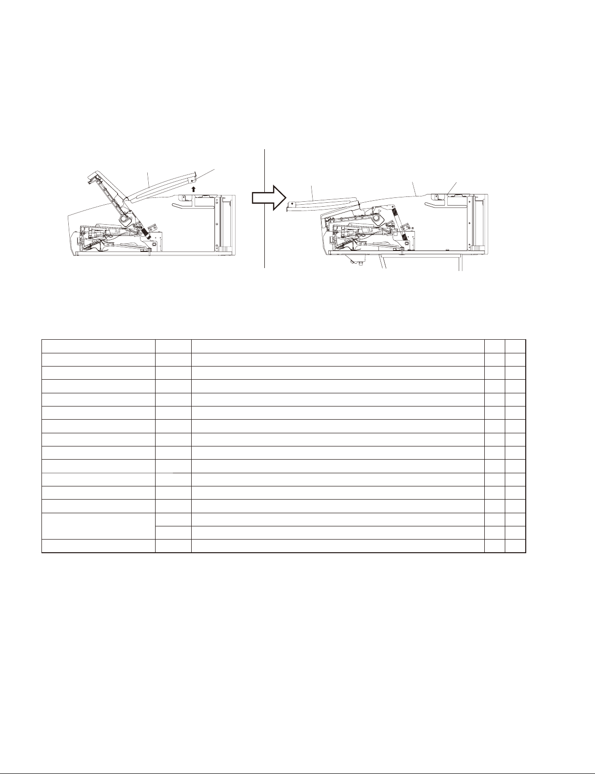
4. Top Board Assembly
(Time required : About 1 minute)
4-1. Open the key cover a little so that the screws marked
[80] can be seen.
4-2. Remove the screw marked [80] from both sides of the
assembly. Move the top board assembly rearward, and
it can then be removed by lifting up. (Fig. 4)
Top board assembly
(屋根Assy)
Key cover(回転蓋)
[80]
4. 屋根 Assy
(所要時間:約 1 分)
4-1. [80] のネジが見えるように、回転蓋を少し開けます。
4-2. [80] のネジを左右外し、屋根 Assyを後方へずらし
た後、持ち上げて外します。(図 4)
[80]
Top board assembly(屋根Assy)
[80]: CapHeadScrew(小ネジ+ CUP)
3.0x8MFZN2B3(WE997800)
(Fig.4)(図 4)
(Fig.4-1)(図 4-1)
13
CVP-405/CVP-405PE/CVP-405PM
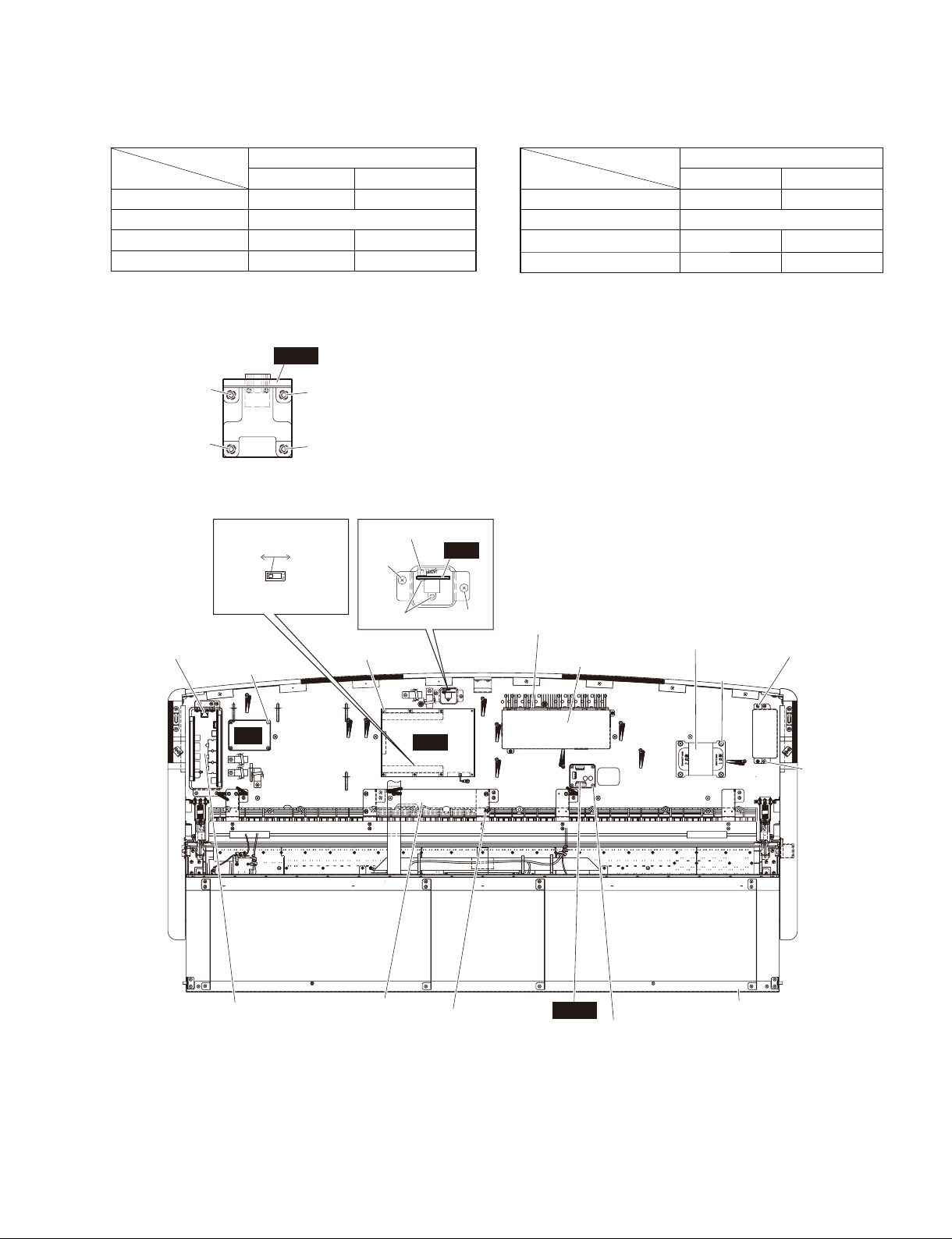
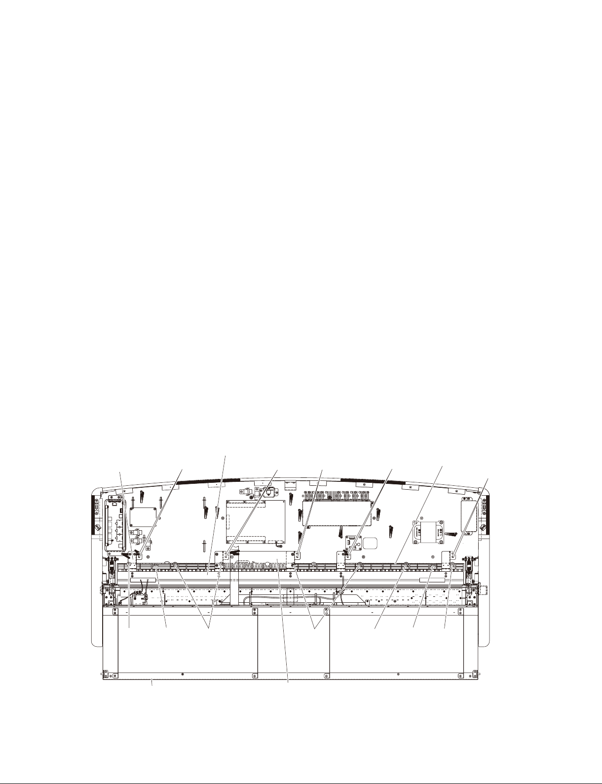
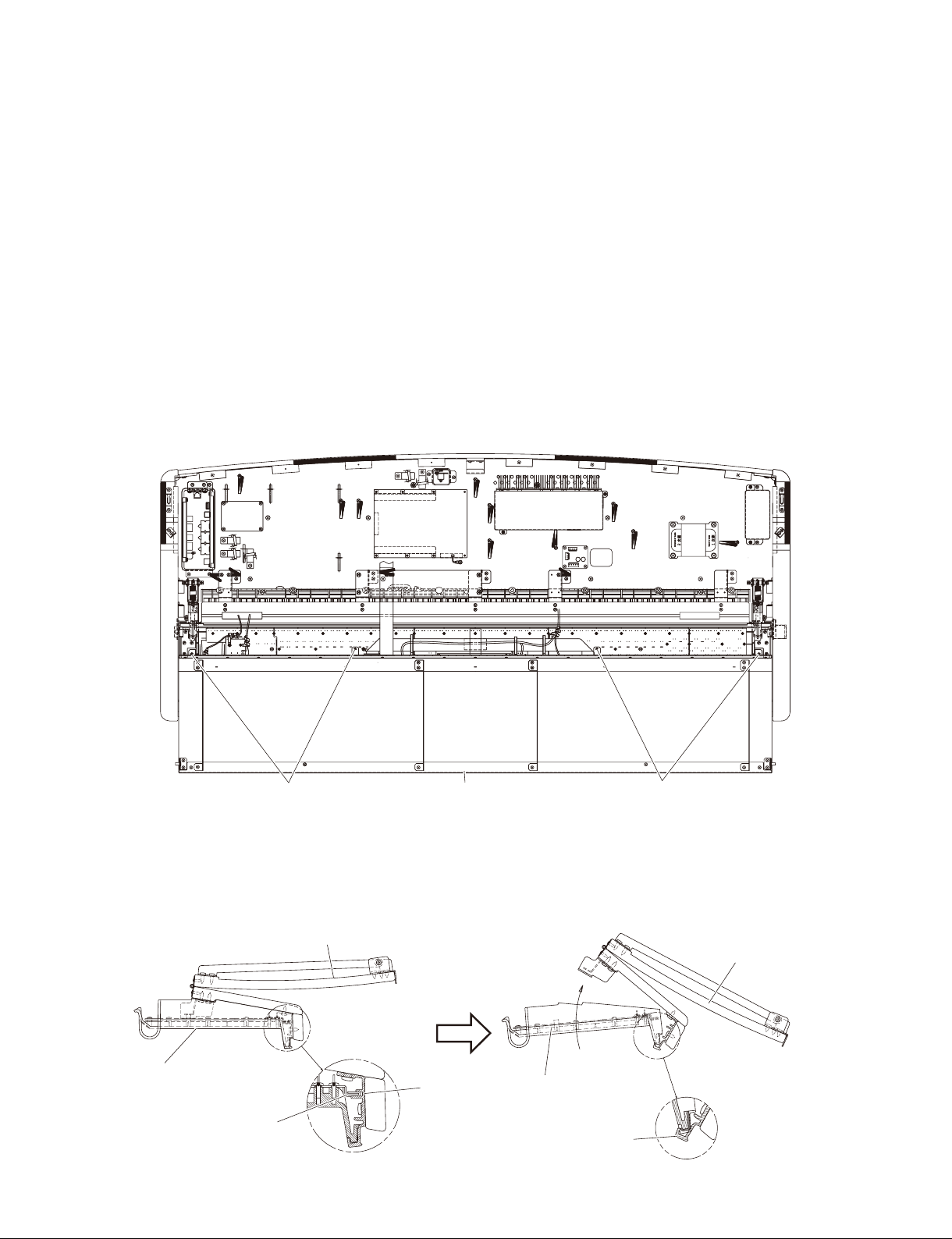
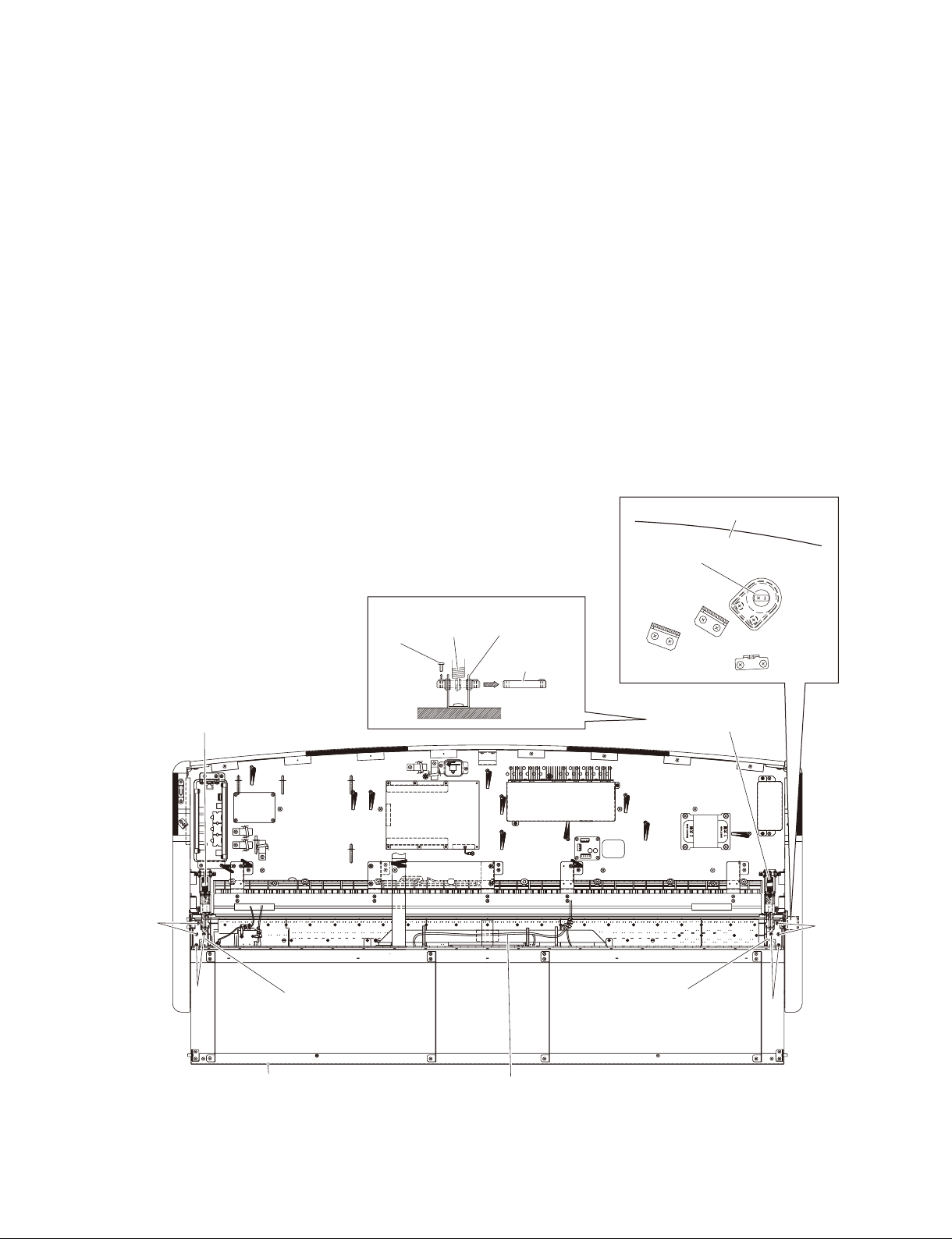
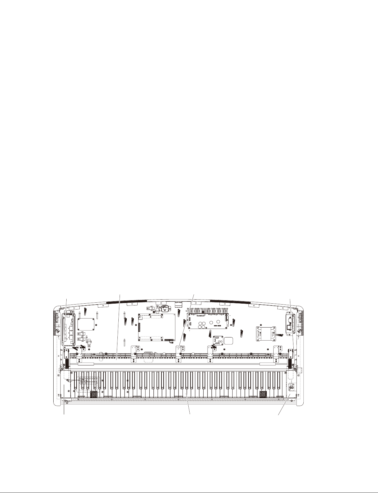
5. Circuit Boards and Assembles (Main Unit Section)
(Time required: About 5 minutes each)
5-1. Remove the top board assembly. (See procedure 4)
5-2. Slide the key cover rearward, remove its guide pin
of the back key cover from the opening for the arm.
5. 基板とアッセンブリ(メインユニット部)
(所要時間:各約 5 分)
5-1. 屋根 Assyを外します。(4 項参照)
5-2. 回転蓋を後方へスライドし、回転蓋(後)のガイドピ
ンを腕 木の抜き口から出して、回転 蓋(後)を開けま
す。(図 5)
Then the back key cover can be opened. (Fig. 5)
Back key cover
(回転蓋(後))
5-3. Each circuit board and assembly can be removed by
removing its fi xing screws as listed below.
Circuit board and Assembly Ref. No. Screw QTY Fig.
PKConnector(PK コネクタ) 70A BindHeadTappingScrew-1(TP#1 + BIND)3.5x11MFZN2W3(WF831100) 2 6
PJK 23c BindHeadTappingScrew-B(B タイト+ BIND)3.0x8MFZN2B3(WE774400) 2 6
DM 76A BindHeadTappingScrew-B(B タイト+ BIND)3.0x8MFZN2W3(WE774300) 6 6
LANAssembly 70B BindHeadTappingScrew-1(TP#1 + BIND)3.5x11MFZN2W3(WF831100) 2 6
LANH 24c BindHeadTappingScrew-B(B タイト+ BIND)3.0x8MFZN2W3(WE774300) 4 6
JackAssembly
MACover(Umodelonly) 109A BindHeadTappingScrew-1(TP#1 + BIND)3.5x11MFZN2W3(WF831100) 2 6
MA80SAssembly 70D BindHeadTappingScrew-1(TP#1 + BIND)3.5x11MFZN2W3(WF831100) 2 6
FUCover(Umodelonly) 109B BindHeadTappingScrew-1(TP#1 + BIND)3.5x11MFZN2W3(WF831100) 2 6
FU60Assembly 70E BindHeadTappingScrew-1(TP#1 + BIND)3.5x11MFZN2W3(WF831100) 2 6
EQ 79A BindHeadTappingScrew-1(TP#1 + BIND)3.5x20MFZN2W3(WE971500) 4 6
NET1 79B BindHeadTappingScrew-1(TP#1 + BIND)3.5x20MFZN2W3(WE971500) 4 6
PowerTransformer
(電源トランス)
Crosspiece(棚板桟) 98 BindHeadTappingScrew-B(B タイト+ BIND)3.0x12MFZN2W3(WE987400) 4 6
*1
70C BindHeadTappingScrew-1(TP#1 + BIND)3.5x11MFZN2W3(WF831100) 3 6
78 BindHeadScrew( 小ネジ+ BIND)4.0x12MFZN2W3(WE968400) 4 6
120A FlatWsher( 平座みがき丸 )4.0x12x1.0MFZN2W3(WF578800)(Umodelonly) 4 6
Guide pin
(ガイドピン)
Back key cover
(回転蓋(後))
(Fig.5)(図 5)
5 -3. 次のネジを外すことにより、基 板・アッセンブリを外す
ことが できます。
Arm
(腕木)
Opening for the arm
(抜け口)
*1 To remove the jack assembly, be sure to remove the LAN
assembly fi rst.
14
*1
ジャック Assy を外すときは、先に LANAssy を外します。
CVP-405/CVP-405PE/CVP-405PM
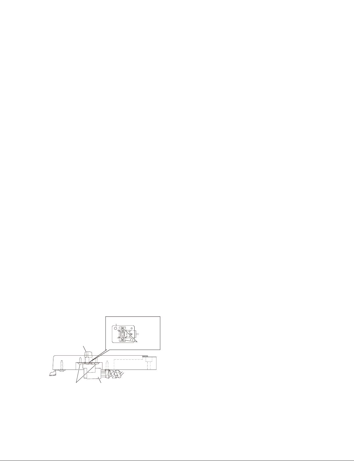
DM circuit board has internal DIP switches for switching the
display in Japanese or in English (SW3).
DIP switch (SW3)
ON OFF
LCD display language Japanese English
VIDEO OUT NTSC/(PAL)
Demonstration music For Japan For other than Japan
Access home page to Server in Japan Server in U.S.A.
* See page 48.
●
LAN Assembly
LANH
[24c]
[24c]
L DIP switch
OFF
ON
SW3
[24c]
[24c]
PK connector
[70A]
PJK
DM シート内には、日本語と英語の表示切替え用 (SW3) のディップス
☞
イッチがあります。
ディップスイッチ(SW3)
ON OFF
LCD 表示言語 日本語 英語
VIDEOOUT NTSC/(PAL)
デモ曲 日本向け 海外向け
ホームページのアクセス先 日本のサーバー 米国のサーバー
※ 48 ページ参照
LAN assembly
[70B] x 2
Jack assembly
(ジャックAssy)
[79A] x 4
EQ
[70C] x 3
[23c]
[76A] x 6
Crosspiece
(棚板桟)
DM
[98] x 4
[70A]
(Fig.6)(図 6)
MA80S assembly
[70D] x 2
MA cover
[109A] x 2
NET1
[79B] x 4
Power transformer
(電源トランス)
[78] x 4
[120A] x 4
Back key cover
(回転蓋(後))
FU cover
[109B] x 2
FU60
assembly
[70E] x 2
1515

CVP-405/CVP-405PE/CVP-405PM
6. AJACK and DJACK Circuit Boards
(Time required : About 10 minutes each)
6-1. Remove the top board assembly. (See procedure 4)
6-2. Open the back key cover. (See procedure 5-2)
6-3. Remove the LAN assembly. (See procedure 5-3)
6-4. Remove the jack assembly. (See procedure 5-3)
6-5.
DJACK Circuit Board
Remove the two (2) screws marked [7A], the three (3)
screws marked [4A], the hexagonal nut marked [6A]
and the washer marked [5A]. The DJACK circuit
board can then be removed. (Fig. 7)
6-6.
AJACK Circuit Board
Remove the two (2) screws marked [7B], the screw
marked [4B], the four (4) hexagonal nuts marked [6B]
and the four (4) washers marked [5B]. The AJACK
circuit board can then be removed. (Fig. 7)
6
. AJACKシート、DJACKシート
(所要時間:各約 10 分)
6-1. 屋根 Assyを外します。(4 項参照)
6-2. 回転蓋(後)を開けます。(5-2 項参照)
6-3. LANAssyを外します。(5-3 項参照)
6-4. ジャック Assyを外します。(5-3 項参照)
DJACKシート
6-5.
[7A] のネジ 2 本、[4A] のネジ 3 本、[6A] の特 殊六
角ナット1 個、[5A] のワッシャー 1 個を外し、DJACK
シートを外します。(図 7)
AJACKシート
6-6.
[7B] のネジ 2 本、[4B] のネジ 1 本、[6B] の特殊六
角ナット 4 個、[5B] のワッシャー 4 個を外し、A J A C K
シートを外します。(図 7)
7. MA80S Circuit Board
(Time required : About 7 minutes)
7-1. Remove the top board assembly. (See procedure 4)
7-2. Open the back key cover. (See procedure 5-2)
7-3. Remove the MA cover assembly.
(See procedure 5-3) (U model only)
7-4. Remove the MA80S assembly. (See procedure 5-3)
7-5. Remove the fi ve (5) screws marked [1A], the three (3)
screws marked [2A] and the screw marked [3A]. The
MA80S circuit board can then be removed. (Fig. 8)
8. FU60 Circ
uit Board
(Time required : About 7 minutes)
8-1. Remove the top board assembly. (See procedure 4)
8-2. Open the back key cover. (See procedure 5-2)
8-3. Remove the FU cover. (See procedure 5-3)
(U model only)
8-4. Remove the FU60 assembly. (See procedure 5-3)
Remove the two (2) screws marked [4C] and the two (2)
8-5.
hexagonal nuts marked [5C]. (Fig. 9) (N model only)
8-6. Remove the two (2) screws marked [1B] and the two
(2) screws marked [6C]. The FU60 circuit board can
then be removed. (Fig. 9)
7. M A8 0S シート(所要時間:約 7 分)
7-1. 屋根 Assyを外します。(4 項参照)
7-2. 回転蓋(後)を開けます。(5-2 項参照)
7-3. M A カバーA ssyを外します。(5-3 項参照)(U モデ
ルのみ)
7-4. M A80SAssyを外します。(5-3 項参照)
7-5. [1A ] のネジ 5 本と [2A ] のネジ 3 本と [3A] のネジ 1
本を外し、MA80S シートを外します。(図 8)
8. FU60 シート
8-1. 屋根 Assyを外します。(4 項参照)
8-2. 回転蓋(後)を開けます。(5-2 項参照)
8-3. FUカバーを外します。(5 -3 項参照)(U モデルのみ)
8-4. FU60Assyを外します。(5-3 項参照)
8-5. [4C] のネジ 2 本と[5C] の六角フランジナット2 個を
外します。(図 9)(N モデルのみ)
8-6. [1B]のネジ2本と[6C]のネジ2本を外し、FU60 シー
トを外します。(図 9)
(所要時間:約 7 分)
16
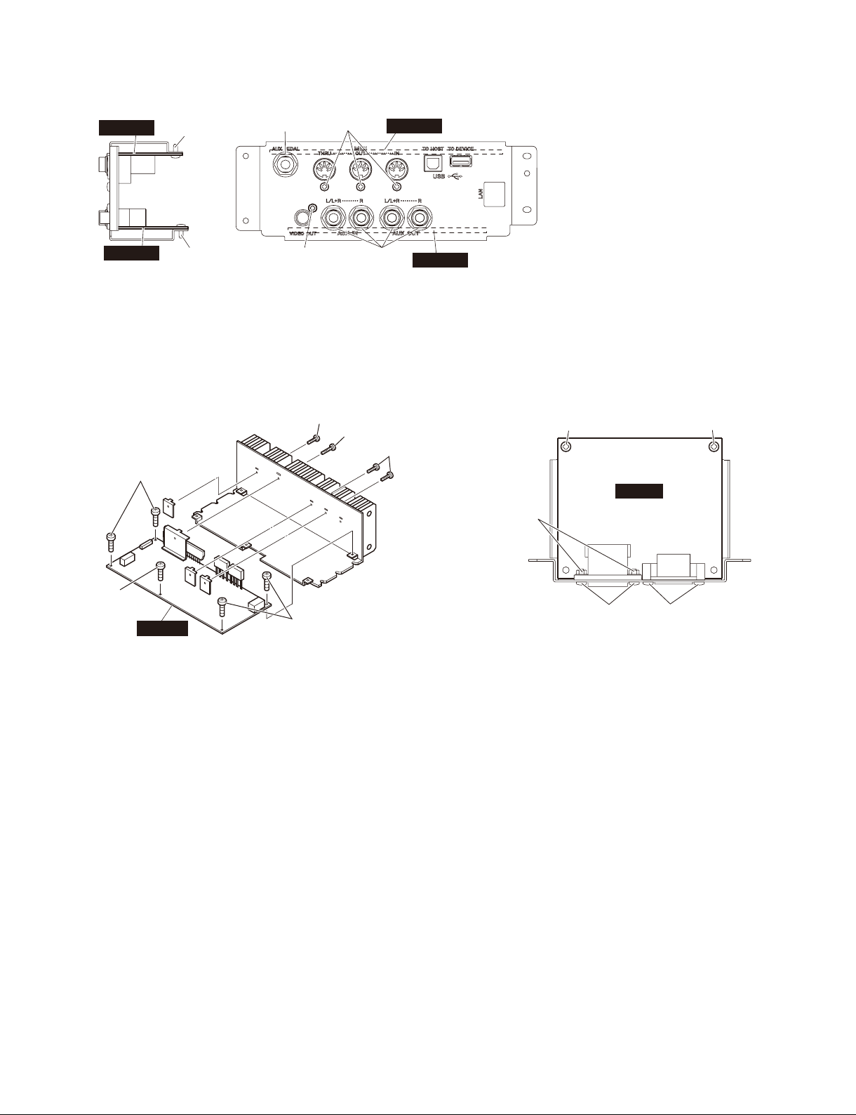
●
Jack Assembly
CVP-405/CVP-405PE/CVP-405PM
DJACK
AJACK
●
MA80S Assembly
[7A] x 2
[7B] x 2
[4A],[4B]: BindHeadTappingScrew-B(B タイト+ BIND)3.0x8MFZN2B3(WE774400)
[5A],[5B]: Washer(ワッシャー)(VJ869400)
[6A],[6B]: HexagonalNut(特殊六角ナット)M12.0x14x2P=1.0(WF559900)
[7A],[7B]: BindHeadTappingScrew-B(B タイト+ BIND)3.0x8MFZN2W3(WE774300)
[1A]
[4B]
[2A]
[4A][6A], [5A]
[3A]
DJACK
[6B], [5B]
Fig.7(図 7)
[2A]
AJACK
●
FU60 Assembly
[5C]
(N model only)
[6C]
[6C]
FU60
[1A]
MA80S
[1A]: BindHeadTappingScrew-B(B タイト+ BIND)
4.0x8MFZN2W3(WE974600)
[2A]: BindHeadTappingScrew-B(B タイト+ BIND)
3.0x10MFZN2W3(WE774200)
[3A]: BindHeadTappingScrew-B(B タイト+ BIND)
3.0x16MFZN2W3(WE973400)
Fig.8(図 8)
[1A]
[4C]
(N model only)
[1B]: BindHeadTappingScrew-B(B タイト+ BIND)
3.0x8MFZN2B3(WE774400)
[4C]: BindHeadScrew(小ネジ+ BIND)
3.0x10MFZN2B3(WF304400)
[5C]: HexagonalNut(六角フランジナット)M3(WF559800)
[6C]: BindHeadTappingScrew-B(B タイト+ BIND)
3.0x12MFZN2W3(WE987400)
Fig.9(図 9)
[1B]
17
CVP-405/CVP-405PE/CVP-405PM
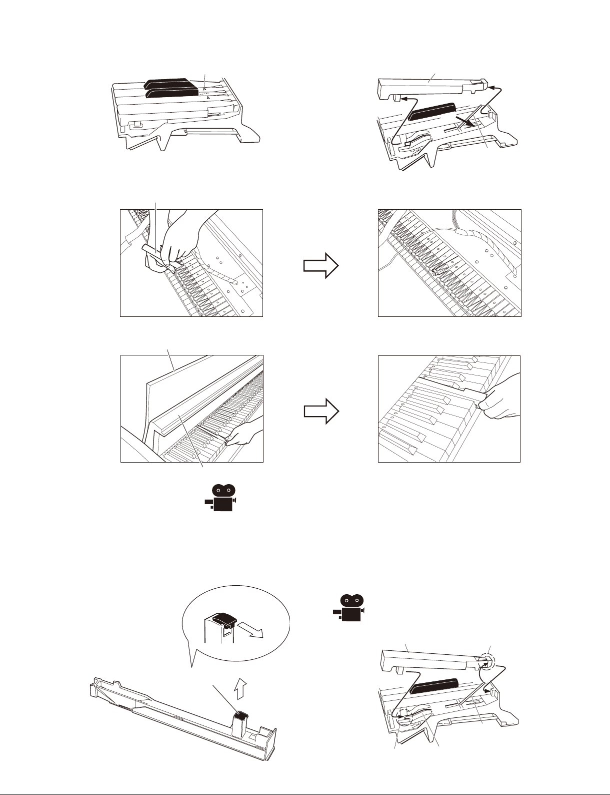
9. White Key, Black Key
(Time required : About 10 minutes)
9-1. Remove the top board assembly. (See procedure 4)
9-2. Open the back key cover. (See procedure 5-2)
9-3. Remove the crsspiece. (See procedure 5-3)
9-4. Remove the ten (10) screws marked [70F]. The MT
angle assembly and angle assembly can then be
removed. (Fig. 10)
9-5. Remove the seven (7) screws marked [72] and the two
(2) screws marked [73], move the keyboard assembly
rearward. (Fig. 10)
9-6.
White key
In order to release the white key from the stopper,
insert a thin plate between the white keys (gap in
the direction indicated by the triangle mark, near the
fulcrum of the key), press down the stopper marked
[A] and move the white key forward. Then the white
key being released from the stopper lifts up. (Fig. 11,
12, 13)
* Use special care not to move the white key forward so
much as to cause damage to the key spring.
9-7. Hold the key cover assembly under your arm. In this
state, move the white key rearward a little. Then the
white key can be removed. (Fig. 14)
9-8.
Black key
The black key can be removed after the white keys on
either side have been removed.
9-9.
Actuate Rubber
Remove the actuate rubber. (Fig. 15)
9. 白鍵、黒鍵(所要時間:約 10 分
9-1. 屋根 Assyを外します。(4 項参照)
9-2. 回転蓋(後)を開けます。(5-2 項参照)
9-3. 棚板桟を外します。(5-3 項参照)
9-4. [70F]のネジ10本を外し、アングル MTAssyと目隠
し金具 Assyを外します。(図 10)
9-5. [72]のネジ7本、[73]のネジ2本を外し、GH3鍵盤
を後方にずらします。(図 10)
白鍵
9-6.
白鍵をストッパーから外すために、薄い金尺状のもの
を鍵盤の間に挿入して(三角マークの示す方向側の隙:
白鍵盤支点付近)、[A ] のストッパーを下げ、白鍵を
前方にずらします。外れると白鍵が浮きます。
(図 11,12,13)
※ このとき、白鍵を前方にずらしすぎてスプリングを傷めない
ように十 分 注 意して作 業をしてください。
9-7. 回転蓋(前/後)を脇に抱えます。この状態から、白
鍵を後方に少しずらし、白鍵を外します。(図 14)
黒鍵
9-8.
黒鍵は、両隣の白鍵を外すと、外すことができます。
駆動ラバー
9-9.
白鍵(黒鍵)の駆動ラバーを外します。(図 15)
)
18
MT angle assembly
(アングルMTAssy)
[72] [72] [72] [72] [72]
Back key cover(回転蓋[後])
[70F]: BindHeadTappingScrew-1(TP#1 + BIND)3.5x11MFZN2W3(WF831100)
[72]: PanHeadScrew(小ネジ+ PAN)SW5.0x25MFZN2W3(WF001500)
[73]: BindHeadTappingScrew-1(TP#1 + BIND)4.0x14MFZN2W3(WE971900)
Angle assembly(目隠し金具Assy)
[70F] [70F]
[73] [73]
Crosspiece(棚板桟)
(Fig.10)(図 10)
[70F][70F]
Keyboard assembly
(GH3鍵盤)
[70F]
CVP-405/CVP-405PE/CVP-405PM
Triangle mark(三角マーク)
(Fig.11)(図 11)
Thin metal plate etc(薄い金尺等)
Back key cover(回転蓋(後))
White key(白鍵)
[A]
Spring
(スプリング)
(Fig.12)(図 12)
(Fig.13)(図 13)
Front key cover(回転蓋(前))
9-10.
Assembling the White Key (Black Key)
If the illustration of a camera is clicked, an animation will flow.
(カメラのイラストをクリックすると動画が流れます。)
(Fig.14)(図 14)
After a key has been fit to part [C] and key guide,
make sure that the spring is fi xed to the key and then
press down part [B] of the key. (Fig. 16)
Remove in this way.
(取り出す)
Actuate rubber
(駆動ラバー)
(Fig.15)(図 15)
白鍵(黒鍵)組立
9-10.
[C]部とキーガイドに白鍵(黒鍵)を加えさせ、鍵盤
の支点内側のばね受け部に、スプリングが確実に入っ
ていることを確認したら、[B] 部の上を下方向にゆっ
くり 押 し 込 んで 取り 付 け ま す。(図 16)
If the illustration of a camera is clicked, an animation will flow.
(カメラのイラストをクリックすると動画が流れます。)
White key(白鍵)
[C]
Key guide(キーガイド)
(Fig.16)(図 16)
[B]
Spring
(スプリング)
19
CVP-405/CVP-405PE/CVP-405PM
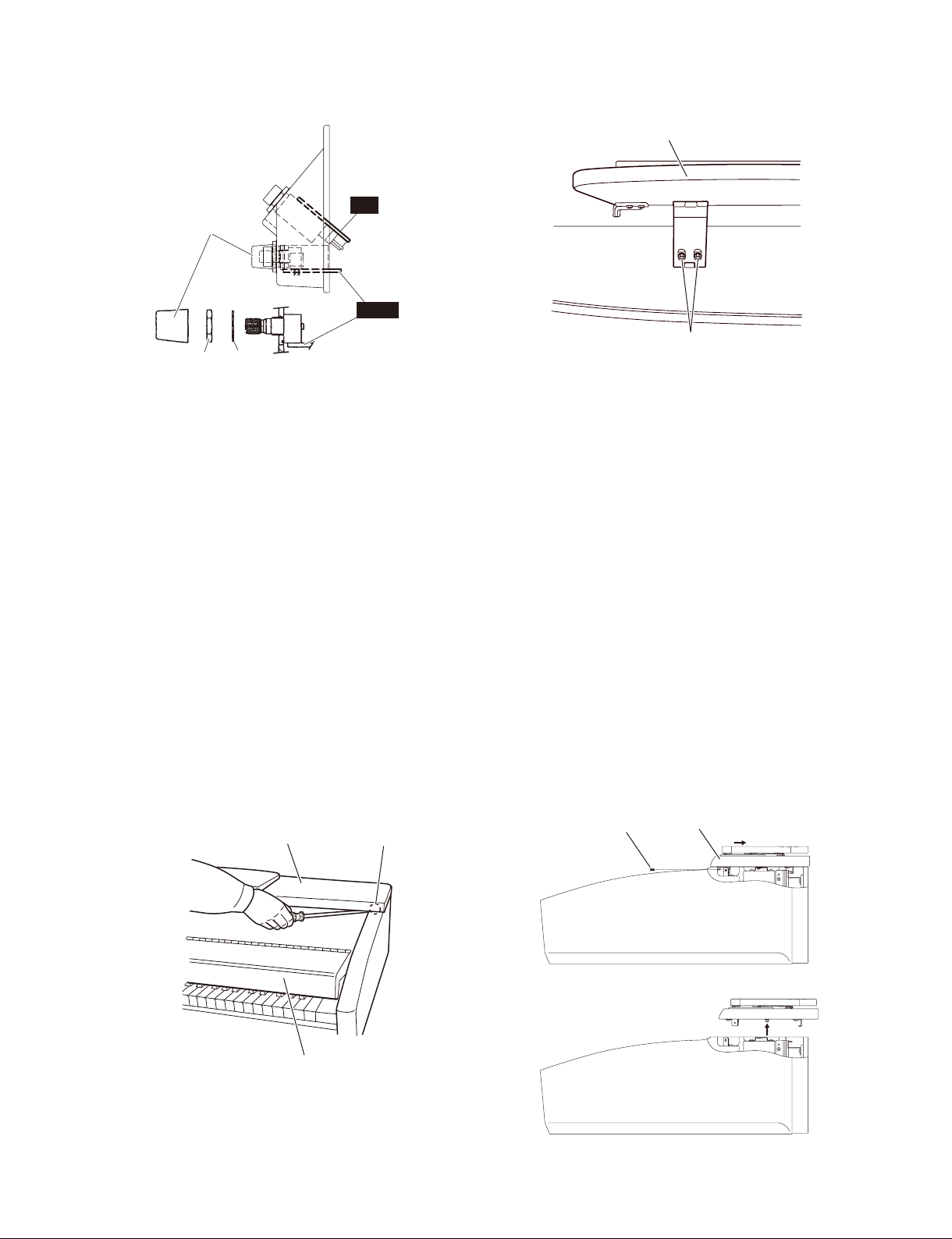
10. Key Cover Assembly
(Time required: About 5 minutes)
10-1. Remove the top board assembly. (See procedure 4)
10-2. Open the back key cover. (See procedure 5-2)
10-3. Remove the four (4) screws marked [3B]. (Fig. 17)
10-4. Using the tip end of the panel as the fulcrum, pull up
the key cover assembly to remove it. (Fig. 18)
Installation of Key Cover
Fit the sash of the key cover over the tip end of the
panel and install the key cover, using care for the
balance between right and left. When the key cover
is installed properly, lugs of the panel (CP holders) at
6 locations should fi t in the groove in the key cover.
If there is a lug (CP holder) that is not fitted in the
groove, push around it so that it will fi t in the groove.
(Fig. 18, Fig. 19)
10. 回転蓋(所要時間:約 5 分)
10-1. 屋根 Assyを外します。(4 項参照)
10-2. 回転蓋(後)を開けます。(5-2 項参照)
10-3. [3B] のネジ 4 本を外します。(図 17)
10- 4. パネルの先端を支点として回転蓋を引き上げて、回
転蓋を外します。(図 18)
回転蓋の取り付け方法
回転蓋のサッシをパネルの先端に掛け、左右ずれないよう
に回転蓋を装着します。
正常に装着されるとパネルの突起(CP 固定金具)6 箇所が
回転蓋のサッシの溝に嵌まります。
このパネル の 突 起(CP 固定金具)部がサッシの溝に嵌まら
ないときは、CP 固定金具付近を押して、サッシの溝に嵌め込
みます。(図 18、図 19)
●
Key Cover & Panel Assembly
<Side view /
Panel assembly
(パネルAssy)
側面
>
20
[3B]
[3B]: BindHeadTappingScrew-B(B タイト+ BIND)3.0x10MFZN2W3(WE774200)
(回転蓋 Assy)
Key cover(回転蓋)
CP holder
(CP固定金具)
Back key cover(回転蓋(後))
(Fig.17)(図 17)
Groove
(溝)
(Fig.18)(図 18)
Panel assembly
(パネルAssy)
Sash
(サッシ)
[3B]
Key cover
(回転蓋)

CVP-405/CVP-405PE/CVP-405PM
11. Circuit Boards and Assembles (Panel Assembly Section)
(Time required: About 10 minutes each)
11-1. Remove the top board assembly. (See procedure 4)
11-2. Open the back key cover. (See procedure 5-2)
11-3. Remove the key cover assembly. (See procedure 10)
11-4. Put cloth or the like between the panel assembly and
keyboard to prevent the panel assembly from being
distorted.
11. 基板とアッセンブリ(パネル Assy部)
(所要時間:各約 10 分)
11-1. 屋根 Assyを外します。(4 項参照)
11-2. 回転蓋(後)を開けます。(5-2 項参照)
11-3. 回転蓋を外します。(10 項参照)
11-4. パネル Assyと鍵盤との隙間に布等を入れて、パネル
Assyが歪まないようにします。
11-5. 次のネジを外すことにより、基板・アッセンブリを外す
ことが できます。
11-5. Remove the screws listed below. Then the circuit
board and assembly can be removed.
Circuit board and Assembly Ref. No. Screw QTY Fig.
SpeakerAssembly(LorR)
(スピーカ Assy)
Speaker(LorR)(スピーカ) 70c BindHeadTappingScrew-B(B タイト+ BIND)3.0x8MFZN2B3(WE774400) 4 19
EIF
*1
USB
MV2
INV 510G BindHeadTappingScrew-B(B タイト+ BIND)3.0x8MFZN2W3(WE774300) 4 19
LCDAssembly(LCDAssy)
PNL2
PNL1+PNL2
ENC+PNC
PNR1+PNR2
PanelL
(パネル木部集成 L)
PanelR
(パネル木部集成 R)
SpeakerGrille(LorR)
(スピーカグリル)
*2
PNL1
ENC
*3
PNC
PNR1
*4
PNR2
*5
*6
*7
510A BindHeadTappingScrew-B(B タイト+ BIND)3.0x8MFZN2W3(WE774300) 4 19
510B BindHeadTappingScrew-B(B タイト+ BIND)3.0x8MFZN2W3(WE774300) 3 19
510C BindHeadTappingScrew-B(B タイト+ BIND)3.0x8MFZN2W3(WE774300) 1 19
510D BindHeadTappingScrew-B(B タイト+ BIND)3.0x8MFZN2W3(WE774300) 3 19
510E BindHeadTappingScrew-B(B タイト+ BIND)3.0x8MFZN2W3(WE774300) 2 19
Knob(MASTERVOLUME)(V ツマミ) 1 19
510F BindHeadTappingScrew-B(B タイト+ BIND)3.0x8MFZN2W3(WE774300) 4 19
510H BindHeadTappingScrew-B(B タイト+ BIND)3.0x8MFZN2W3(WE774300) 4 19
510C BindHeadTappingScrew-B(B タイト+ BIND)3.0x8MFZN2W3(WE774300) 1 19
510I BindHeadTappingScrew-B(B タイト+ BIND)3.0x8MFZN2W3(WE774300) 5 19
510J BindHeadTappingScrew-B(B タイト+ BIND)3.0x8MFZN2W3(WE774300) 1 19
510J BindHeadTappingScrew-B(B タイト+ BIND)3.0x8MFZN2W3(WE774300) 1 19
510K BindHeadTappingScrew-B(B タイト+ BIND)3.0x8MFZN2W3(WE774300) 13 19
510L BindHeadTappingScrew-B(B タイト+ BIND)3.0x8MFZN2W3(WE774300) 2 19
EncoderKnob(DATAENTRY)(エンコーダツマミ) 1 19
510M BindHeadTappingScrew-B(B タイト+ BIND)3.0x8MFZN2W3(WE774300) 4 19
510L BindHeadTappingScrew-B(B タイト+ BIND)3.0x8MFZN2W3(WE774300) 2 19
510N BindHeadTappingScrew-B(B タイト+ BIND)3.0x8MFZN2W3(WE774300) 14 19
510O BindHeadTappingScrew-B(B タイト+ BIND)3.0x8MFZN2W3(WE774300) 1 19
510O BindHeadTappingScrew-B(B タイト+ BIND)3.0x8MFZN2W3(WE774300) 1 19
510P BindHeadTappingScrew-B(B タイト+ BIND)3.0x8MFZN2W3(WE774300) 13 19
510Q BindHeadTappingScrew-B(B タイト+ BIND)3.0x8MFZN2W3(WE774300) 2 19
510Q BindHeadTappingScrew-B(B タイト+ BIND)3.0x8MFZN2W3(WE774300) 2 19
510R BindHeadTappingScrew-B(B タイト+ BIND)3.0x8MFZN2W3(WE774300) 7 19
510S BindHeadTappingScrew-B(B タイト+ BIND)3.0x8MFZN2W3(WE774300) 6 19
520A BindHeadTappingScrew-1(TP#1 + BIND)3.5x10MFZN2W3(WE970800) 6 19
510T BindHeadTappingScrew-B(B タイト+ BIND)3.0x8MFZN2W3(WE774300) 6 19
520B BindHeadTappingScrew-1(TP#1 + BIND)3.5x10MFZN2W3(WE970800) 6 19
A Endlugofgrille(グリルの爪) 8 19
*1 Before replacing the USB circuit board, check to ensure
that USB fl ash memory is not inserted.
*2 It is not possible to remove the harness connecting PNL1
circuit board and PNL2 circuit board.
*3 To remove the ENC circuit board and the PNC circuit
board, be sure to remove the INV circuit board first. It
is not possible to remove the harness connecting ENC
circuit board and PNC circuit board.
*1
USB シート交換前に US B メモリが挿入されていないことを確認
してください。
*2
PNL1 シートと PNL2 シートを接続している束線は、外れません。
*3
ENC シートと PNC シートを外すときは、先に INV シートを外し
ます。ENC シートと PN C シートを接続している束線は、外れま
せん。
21
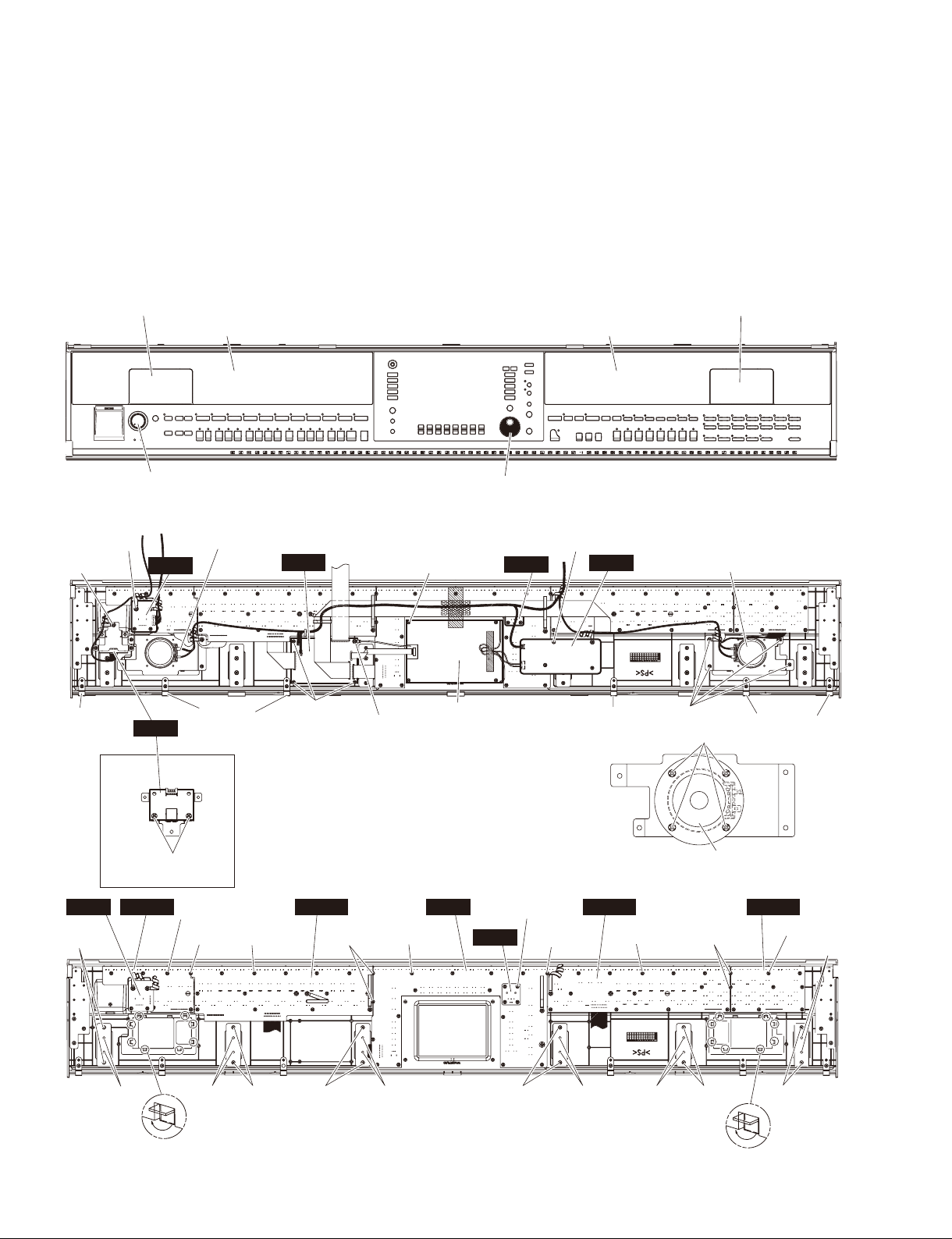
CVP-405/CVP-405PE/CVP-405PM
*4 It is not possible to remove the harness connecting PNR1
circuit board and PNR2 circuit board.
*5 To remove the panel L, be sure to remove the USB circuit
board fi rst.
*6 To remove the panel R, be sure to remove the INV circuit
board fi rst.
*7 To remove the speaker grille, be sure to remove the
speaker assembly fi rst.
Panel Assembly
●
<Top view /
<Bottom view /
[510F] x 4
[510D] x 3
(パネル Assy)
>
上面
Speaker grille L(スピーカグリルL)
Panel L(パネル木部集成L)
Knob(Vツマミ)
>
底面
Speaker assembly L
(スピーカAssyL)
MV2
EIF
[510H] x 4
*4
PNR1 シートと PNR2 シートを接続している束線は、外れません。
*5
パネル木部集成 L
*6
パネル木部集成 R
*7
スピーカグリル
Panel R(パネル木部集成R)
Encoder knob(エンコーダツマミ)
ENC
を外すときは、先に USB シートを外します。
を外すときは、先に INV シートを外します。
を外すときは、先にスピーカ Assy を外します。
Speaker grille R(スピーカグリルR)
[510G] x 4
INV
Speaker assembly R
(スピーカAssyR)
CP holder
(CP固定金具)
MV2
[510S]
[520A]
22
USB
PNL2 PNL1 PNC PNR1 PNR2
Endlugofgrille
(グリルの爪)
CP holder
(CP固定金具)
[510E]
[510I] x 5
[510J]
[A]
[510K] x 13 [510N] x 14
[510S]
[510B]
[510C]
[510L]
LCD assembly
(LCDAssy)
ENC
(Fig.19)(図 19)
[510M] x 4
[510O]
CP holder
(CP固定金具)
[510P] x 13
[520B][520B] [510T][510T][510S] [520A][520A]
[510A]
[70c]
Speaker
(スピーカ)
[510Q]
Endlugofgrille
(グリルの爪)
CP holder
(CP固定金具)
[510R] x 7
[510T]
[A]
[520B]
CVP-405/CVP-405PE/CVP-405PM
12. Panel Assembly
(Time required: About 10 minutes)
12-1. Remove the top board assembly. (See procedure 4)
12-2. Open the back key cover. (See procedure 5-2)
12-3. Remove the key cover assembly. (See procedure 10)
12-4. Remove the screw marked [82], pull off the rod from
the spring holder and remove the spring R. (Fig. 20)
* Remove the spring L in the same manner.
12-5. Put cloth or the like between the panel assembly and
keyboard.
12-6. Remove the four (4) screws marked [83] and then
remove the turning axle assembly R from the panel
assembly. (Fig. 20)
* When installing the turning axle assembly R, carefully
check for the direction of the damper (turning axle)
on the side of the arm assembly R. The turning axle
assembly R should be installed in such direction that
letters ("TH") stamped on the damper (turning axle) is
upside down. Installation otherwise will damage the
damper.
12-7. Remove the turning axle assembly L in the same
manner. (Fig. 20)
* Be sure to remove the turning axle assembly R fi rst.
12-8. Remove the panel assembly. (Fig. 20)
12. パネル Assy(所要時間:約 10 分)
12-1. 屋根 Assyを外します。(4 項参照)
12-2. 回転蓋(後)を開けます。(5-2 項参照)
12-3. 回転蓋を外します。(10 項参照)
12-4. [82] のネジ 1 本を外し、バネ軸 (A ) をバネ固定金具
から抜いて、バネ ( R ) を外します。(図 20)
※ バネ (L) も同様に外します。
12-5. パネル Assyと鍵盤との隙間に布等を入れます。
[83] のネジ4 本を外し、パネル Assyから回転軸
12-6.
Assy(R) を外します。(図 20)
※ 回転軸Assy(R) を取り付ける際、腕木 (R) 側にあるダンパー
(回転軸)の向きに注意して取り付けてください。
ダンパー(回転軸)に刻印されている文字(TH)が逆さま
になる向きで回転軸 Assy(R) を取り付けます。向きが違う
状態で組み立てるとダンパーが破損します。
12-7. 回転軸 Assy(L) も同様に外します。(図 20)
※ 回転軸 Assyは、(R)側から先に外します。
12-8. パネル Assyを外します。(図 20)
Arm R(腕木R)
Damper
(ダンパー)
[83]
Spring L(バネL)
[83]
[82]
Turning axle assembly L
(回転軸AssyL)
Spring R
(バネR)
Spring holder
(バネ固定金具)
Rod
(バネ軸A)
Spring R(バネR)
Turning axle assembly R
(回転軸AssyR)
[83]
[83]
Back key cover(回転蓋(後))
[82]: BindHeadScrew(小ネジ+ BIND)3.0x8MFZN2W3(WE987200)
[83]: BindHeadTappingScrew-B(B タイト+ BIND)3.0x10MFZN2W3(WE774200)
Panel assembly(パネルAssy)
(Fig.20)(図 20)
23
CVP-405/CVP-405PE/CVP-405PM
13. Key Cover & Panel Assembly
(Time required: About 10 minutes)
13-1. Remove the top board assembly. (See procedure 4)
13-2. Open the back key cover. (See procedure 5-2)
13-3. Remove the spring L and R. (See procedure 12-4)
13-4. Put cloth or the like between the panel assembly and
keyboard.
13-5. Remove the turning axle assembly R from the panel
assembly. (See procedure 12-6)
13-6. Remove the turning axle assembly L from the panel
assembly. (See procedure 12-7)
13-7. Remove the key cover and panel assembly. (Fig. 20)
14. End Block Assembly (L, R)
(Time required : About 15 minutes)
14-1. Remove the top board assembly. (See procedure 4)
14-2. Open the back key cover. (See procedure 5-2)
14-3. Remove the key cover and panel assembly.
(See procedure 13)
14-4. Remove the crosspiece. (See procedure 5-3)
14-5. Remove the MT angle assembly and angle assembly.
(See procedure 9-4)
14-6. Remove the screw marked [74], the spring washer
marked [96] and the fl at washer marked [86]. The end
block assembly can then be removed. (Fig. 21)
* The left and right end block assembly can then be
removed in the same manner.
13. 回転蓋 Assy(回転蓋 + パネル Assy)
(所要時間:約 10 分)
13-1. 屋根 Assyを外します。(4 項参照)
13-2. 回転蓋(後)を開けます。(5-2 項参照)
13-3. バネ(L・R)を外します。(12-4 項参照)
13-4. パネル Assyと鍵盤との隙間に布等を入れます。
13-5. パネル Assyから回転軸Assy(R) を外します。
(12-6項参照)
13-6. パネル Assyから回転軸Assy(L) を外します。
(12-7項参照)
13-7. 回転蓋 Assyを外します。(図 20)
14. 拍子木 Assy(L・R)(所要時間:約 15 分)
14-1. 屋根 Assyを外します。(4 項参照)
14-2. 回転蓋(後)を開けます。(5-2 項参照)
14-3. 回転蓋 Assyを外します。(13 項参照)
14-4. 棚板桟を外します。(5-3 項参照)
14-5. アングル MTAssy+目隠し金具 Assyを外します。
(9-4項参照)
[74] の ネジ 1 本、[96] の バ ネ 座 金 1 個、[86] の 平
14-6.
座小型丸 1 個を外し、拍子木 Assy ( L) を外します。
(図 21)
※ 拍子木 Assy( R ) も同 様に外すことができます。
[74], [96], [86]
End block assembly L
(拍子木AssyL)
(目隠し金具Assy)
[74]: BindHeadTappingScrew-B(B タイト+ BIND)4.0x25MFZN2B3(WF000000)
[86]: FlatWasher(平座小型丸)4.0x8x0.8MFZN2W3(WF578600)
[96]: SpringWasher(バネ座金)4.0MFZN2W3(WF57690)
Angle assembly
MT angle assembly
(アングルMTAssy)
Keyboard assembly
(GH3鍵盤)
(Fig.21)(図 21)
[74], [96], [86]
End block assembly R
(拍子木AssyR)
24
CVP-405/CVP-405PE/CVP-405PM
15. Keyboard Assembly
(Time required : About 20 minutes)
15-1. Remove the top board assembly. (See procedure 4)
15-2. Open the back key cover. (See procedure 5-2)
15-3. Remove the key cover and panel assembly.
(See procedure 13)
15-4. Remove the crosspiece. (See procedure 5-3)
15-5. Remove the MT angle assembly and angle assembly.
(See procedure 9-4)
15-6. Remove the end block assembly L and R.
(See procedure 14)
15-7. Remove the keyboard assembly.
(See procedure 9-5)
16. Power Switch Assembly
(Time required : About 20 minutes)
16-1. Remove the top board assembly. (See procedure 4)
16-2. Open the back key cover. (See procedure 5-2)
16-3. Remove the key cover and panel assembly.
(See procedure 13)
16-4. Remove the crosspiece. (See procedure 5-3)
16-5. Remove the MT angle assembly and angle assembly.
(See procedure 9-4)
16-6. Remove the end block assembly R.
(See procedure 14)
16-7. Remove the two (2) screws marked [8A]. The power
switch assembly can then be removed from the end
block assembly R. (Fig. 22)
16-8. Remove the push knob. (Fig. 22)
16-9. Remove the two (2) screws marked [6D]. The power
switch assembly can then be removed from the angle.
(Fig. 22)
15. GH3 鍵盤(所要時間:約 20 分)
15-1. 屋根 Assyを外します。(4 項参照)
15-2. 回転蓋(後)を開けます。(5-2 項参照)
15-3. 回転蓋 Assyを外します。(13 項参照)
15-4. 棚板桟を外します。(5 -3 項参照)
15-5. アングル MTAssy+目隠し金具 Assyを外します。
(9-4項参照)
15-6. 拍子木 Assy(L・R)を外します。(14 項参照)
15-7. GH3 鍵盤を外します。(9-5 項参照)
16. PSW 束線(パワースイッチ+束線)
(所要時間:約 20 分)
16-1. 屋根 Assyを外します。(4 項参照)
16-2. 回転蓋(後)を開けます。(5-2 項参照)
16-3. 回転蓋 Assyを外します。(13 項参照)
16- 4. 棚板桟を外します。(5-3 項参照)
16-5. アングル MTAssy+目隠し金具 Assyを外します。
(9-4項参照)
16- 6. 拍子木 Assy(R)を外します。(14 項参照)
16-7. [8A] のネジ 2 本を外し、PSW 束線(アングル PSW 付)
を外します。(図 22)
16-8. プッシュツマミを外します。(図 22)
16-9. [6D] のネジ 2 本を外し、アングル P SW を PSW 束線
から外します。(図 22)
●
End Block Assembly R
<Side view /
(プッシュツマミ)
[6D]: BindHeadTappingScrew-B(B タイト+ BIND)
3.0x6MFZN2W3(WE936300)
[8A]: BindHeadTappingScrew-1(TP#1 + BIND)
3.5x10MFZN2W3(WE970800)
>
側面
Push knob
[8A]
(拍子木 AssyR)
Angle(アングルPSW)
[6D]
Power switch assembly
(PSW束線)
(Fig.22)(図 22)
25
CVP-405/CVP-405PE/CVP-405PM
17. PL Circuit Board
(Time required : About 25 minutes
17-1. Remove the top board assembly. (See procedure 4)
17-2. Open the back key cover. (See procedure 5-2)
17-3. Remove the key cover and panel assembly.
(See procedure 13)
17-4. Remove the crosspiece. (See procedure 5-3)
17-5. Remove the MT angle assembly and angle assembly.
(See procedure 9-4)
17-6. Remove the end block assembly L and R.
(See procedure 14)
17-7. Remove the keyboard assembly. (See procedure 15)
17-8. Remove the screw marked [10A]. The PL circuit
board can then be removed. (Fig. 23)
)
18. Front Rail Assembly
(Time required : About 25 minutes)
18-1. Remove the top board assembly. (See procedure 4)
18-2. Open the back key cover. (See procedure 5-2)
18-3. Remove the key cover and panel assembly.
(See procedure 13)
18-4. Remove the crosspiece. (See procedure 5-3)
18-5. Remove the MT angle assembly and angle assembly.
(See procedure 9-4)
18-6. Remove the end block assembly L and R.
(See procedure 14)
18-7. Remove the keyboard assembly. (See procedure 15)
18-8. Remove the two (2) screws marked [75A] from both
sides of the assembly. (Fig. 24)
18-9. Remove the seven (7) screws marked [71A]. The front
rail assembly can then be removed. (Fig. 25)
17. PL シート(所要時間:約 25 分)
17-1. 屋根 Assyを外します。(4 項参照)
17-2. 回転蓋(後)を開けます。(5-2 項参照)
17-3. 回転蓋 Assyを外します。(13 項参照)
17-4. 棚板桟を外します。(5-3 項参照)
17-5. アングル MTAssy+目隠し金具 Assyを外します。
(9-4項参照)
17-6. 拍子木 Assy(L・R)を外します。(14 項参照)
17-7. GH3 鍵盤を外します。(15 項参照)
17-8. [10A] のネジ 1 本を外し、PL シートを外します。
(図23)
18. 口棒 Assy(所要時間:約 25 分)
18-1. 屋根 Assyを外します。(4 項参照)
18-2. 回転蓋(後)を開けます。(5-2 項参照)
18-3. 回転蓋 Assyを外します。(13 項参照)
18-4. 棚板桟を外します。(5-3 項参照)
18-5. アングル MTAssy+目隠し金具 Assyを外します。
(9-4項参照)
18-6. 拍子木 Assy(L・R)を外します。(14 項参照)
18-7. GH3 鍵盤を外します。(15 項参照)
18-8. [75A] のネジ 2 本を左右外します。(図 24)
18 - 9. [71 A] のネジ 7 本を外し、口棒 Assyを外します。
(図25)
[10A]
PL
Front rail assembly
(口棒Assy)
[10A]: BindHeadTappingScrew-1(TP#1 + BIND)
3.5x10MFZN2W3(WE970800)
(Fig.23)(図 23)
26
Arm assembly L
(腕木AssyL)
Arm assembly L
(腕木AssyL)
[75A]
Front rail assembly
(口棒Assy)
[75A],[75B]:BindHeadTappingScrew-1(TP#1 + BIND)
3.5x16MFZN2W3(WE970700)
(Fig.24)(図 24)
[75B]
Back top board assembly
(背面框)
CVP-405/CVP-405PE/CVP-405PM
19. Back Top Board Assembly
(Time required : About 5 minutes)
19-1. Remove the top board assembly. (See procedure 4)
19-2. Open the back key cover. (See procedure 5-2)
19-3. Remove the three (3) screws marked [75B] from both
sides of the assembly. (Fig. 24)
19-4. Remove the eight (8) screws marked [71B]. The back
top board assembly can then be removed. (Fig. 25)
20. Arm Assembly (L, R)
(Time required : About 40 minutes)
20-1. Remove the top board assembly. (See procedure 4)
20-2. Open the back key cover. (See procedure 5-2)
20-3. Remove the key cover and panel assembly.
(See procedure 13)
20-4. Remove the crosspiece. (See procedure 5-3)
20-5. Remove the MT angle assembly and angle assembly.
(See procedure 9-4)
20-6. Remove the end block assembly L and R.
(See procedure 14)
20-7. Remove the keyboard assembly. (See procedure 15)
20-8. Remove the two (2) screws marked [75A], the three (3)
screws marked [75B] and the fi ve (5) screws marked
[71C]. The arm assembly L can then be removed.
(Fig. 24, 25)
* The arm assembly R can then be removed in the same
manner.
19. 背面框 Assy(所要時間:約 5 分)
19-1. 屋根 Assyを外します。(4 項参照)
19-2. 回転蓋(後)を開けます。(5-2 項参照)
19-3. [75B] のネジ 3 本を左右外します。(図 24)
19 - 4. [71B] のネジ 8 本を外し、背面框 Assyを外します。
(図25)
20. 腕木 Assy(L・R)
20-1. 屋根 Assyを外します。(4 項参照)
20-2. 回転蓋(後)を開けます。(5-2 項参照)
20-3. 回転蓋 Assyを外します。(13 項参照)
20-4. 棚板桟を外します。(5-3 項参照)
20-5. アングル MTAssy+目隠し金具 Assyを外します。
(9-4項参照)
20-6. 拍子木 Assy(L・R)を外します。(14 項参照)
20-7. GH3 鍵盤を外します。(15 項参照)
20-8. [75A] のネジ 2 本、[75B] のネジ 3 本、[71C] のネジ
5本を外し、腕木Assy(L) を外します。
(図24、図25)
※ 腕木 Assy( R ) も同様に外すことができます。
(所要時間:約 40 分)
<Bottom view /
Arm assembly L
(腕木AssyL)
[71C]
[71C]
[71C]
>
底面
Front rail assembly
[71A]
[71B]
[71A],[71B],[71C]:TrussHeadTappingScrew-1(TP#1 + TRUS)3.5x25MFZN2B3(WE970400)
[71B]
Back top board assembly
(口棒Assy)
[71A]
(背面框)
(Fig.25)(図 25)
[71B]
[71A]
[71A]
[71B]
Arm assembly R
(腕木AssyR)
27
CVP-405/CVP-405PE/CVP-405PM
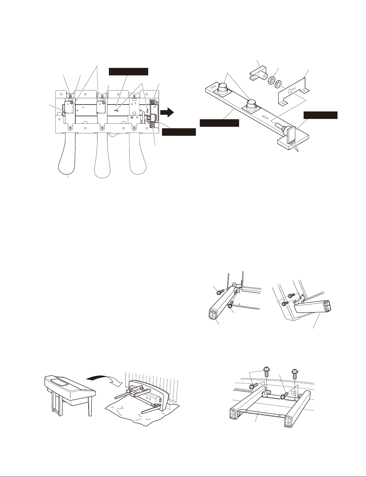
21. Pedal Box Assembly, Pedal Assembly
(Time required : About 5 minutes)
21-1. Remove the cap from the rear leg L, and disconnect
the PK-LF cable. (fi g. 26)
21-2. Remove the two (2) screws marked [11aA]. The pedal
box assembly can then be removed. (Fig. 26)
21-3. Remove the adjuster. (Fig. 27)
21-4. Remove the eight (8) screws marked [7C] and the
screw marked [10B]. The pedal assembly can then be
removed. (Fig. 27)
21-5. Remove the three (3) screws marked [9]. The pedal
box can then be removed. (Fig. 27)
Cap(キャップ)
Rear leg L
(後脚L)
PK-LF cable
(PKケーブル)
21. ペダル BoxAssy、ペダル Assy
(所要時間:約 5 分)
21-1. 後脚のキャップ、PK ケーブルを外します。(図 26)
21-2. [11aA] のネジ 2 本を外し、ペダル BoxAssy を外し
ます。(図 26)
21-3. アジャスターを外します。(図 27)
21-4. [7C] のネジ 8 本、[10B] のネジ 1 本を外し、ペダル
Assyを外します。(図 27)
21-5. [9] のネジ 3 本を外し、ペダルボックス集 成を外します。
(図 27)
●
Pedal Box Assembly
<Bottom view /
Pedal box
(ペダルボックス集成)
[7C]
[10B]
[9]
(ペダル BoxAssy)
>
底面
Adjuster(アジャスター)
Pedal assembly
(ペダルAssy)
[7C]
[9]
Pedal box assembly
(ペダルBoxAssy)
[11aA]:BindHeadScrew(小ネジ+ BIND)5.0x18MFZN2B3
(WF741300)
(Fig.26)(図 26)
[11aA]
22. PEDAL (SW) Circuit Board and PEDAL VR Circuit Board
(Time required : About 10 minutes)
22-1. Remove the cap from the rear leg L, and disconnect
the PK-LF cable. (fi g. 26)
22-2. Remove the pedal box assembly. (See procedure 21)
22-3. Remove the adjuster. (Fig. 27)
22-4. Remove the pedal assembly. (See procedure 21)
22-5. Remove the two (2) screws marked [270]. The two (2)
actuators can then be removed. (Fig. 28)
22-6. Remove the screw marked [120B]. The pedal piece L
can then be removed. (Fig. 28)
22-7. Straighten the three (3) bent frame portions marked
[A] securing the PEDAL (SW) circuit board using
pliers or the like and remove the two (2) screws
marked [120C]. Lift the PEDAL (SW) circuit board
together with the PEDAL VR circuit board a little and
then slide to the right to remove them. (Fig. 28)
22-8. Remove the two (2) rubber contacts from the PEDAL
(SW) circuit board. (Fig. 29)
22-9. Pull out the VR actuator from the PEDAL VR circuit
board and remove the hexagonal nut marked [B]. The
VR holder can then be removed. (Fig. 29)
Remove the soldering connecting the PEDAL (SW)
circuit board and PEDAL VR circuit board to separate
28
the PEDAL (SW) circuit board from the PEDAL VR
circuit board. (Fig. 29)
[7C]: BindHeadTappingScrew-1(TP#1 + BIND)
4.0x14MFZN2W3(WE971900)
[9]: TrussHeadTappingScrew-B(B タイト+ TRUS)
4.0x20MFZN2B3(WE975100)
[10B]: TrussHeadTappingScrew-1(TP#1 + TRUS)
3.5x14MFZN2W3(WE970500)
(Fig.27)(図 27)
22. PEDAL(SW) シート、PEDALVR シート
(
22-1. 後脚のキャップ、PK ケーブルを外します。(図 26)
22-2. ペダル BoxAssyを外します。(21 項参照)
22-3. アジャスターを外します。(図 27)
22-4. ペダル Assyを外します。(21 項参照)
22-5. [270] のネジ 2 本を外して、アクチュエータを 2 個外し
22-6. [120B] のネジ 1 本を外して、ペダル本体 (L) を外し
22-7. PEDAL(SW ) シートを止めている [A] のフレーム折り
22-8. PEDAL(SW ) シートから接点ゴム 2 個を外します。
(図29)
22-9. PEDALV R シートから VR アクチュエータを抜き、[B]
PEDAL(SW)シートとPEDALVR シートを取り付け
所要時間:約 10 分)
ます。(図 28)
ます。(図 28)
曲げ部 3 箇所をペンチ等で真直ぐに戻し、[120C] の
ネジ 2 本を外して、PEDAL(SW) シートと PEDAL
VRシートを一緒に右方向にスライドさせて外します。
(図 28)
の六角ナット1 個を外して、可変抵抗取付金具を外し
ます。(図 29)
ている半田を取り除いて、それぞれのシートに分けま
す。(図 29)
CVP-405/CVP-405PE/CVP-405PM
●
Pedal Assembly
<Top view /
[120B]
[A]
(ペダル Assy)
>
上面
Actuator
(アクチュエータ)
[270]
[270]
PEDAL (SW)
[A]
[120C]
PEDAL VR
[120C]
Pedal piece L
(ペダル本体(L))
[120B],[120C]: BindHeadTappingScrew-B(B タイト+ BIND)
3.0x8MFZN2B3(WE774400)
[270]: BindHeadTappingScrew-B(B タイト+ BIND)
3.0x10MFZN2W3(WE774200)or
BindHeadTappingScrew-B(B タイト+ BIND)
3.0x8MFZN2B3(WE774400)
(Fig.28)(図 28)
23. Front and Rear Leg Assembly
(Time required : About 15 minutes)
23-1. Remove the pedal box assembly. (See procedure 21)
23-2. With a soft cloth like a blanket placed on the fl oor.
Rest the main unit against the wall gently so that the
keyboard side is faced toward the bottom. (Fig. 30)
* For safety, this work should be done by two persons.
23-3. Remove the four (4) screws marked [11aB]. The front
leg assembly can then be removed. (Fig. 31)
* The left and right front leg assembly each can then be
removed in the same manner.
23-4. Remove the four (4) screws marked [11aC]. The rear
leg assembly can then be removed. (Fig. 32)
VR actuator
Rubber contact
(接点ゴム)
(VRアクチュエータ)
[B]
VR holder
(可変抵抗取付金具)
PEDAL VR
PEDAL (SW)
Solder(半田)
(Fig.29)(図 29)
23. 前脚 Assy(L・R)、後脚 Assy
(所要時間:約 15 分)
23-1. ペダル BoxAssyを外します。(21 項参照)
23-2. 毛布などの柔かい布を床に敷いて、鍵盤側を下にして
本体を床に置き、倒れないように壁に立てかけます。
(図 30)
※ 安全のために、かならず二人で作業してください。
23-3. [11aB] のネジ 4 本を外し、前脚 Assy(R) を外します。
(図31)
※ 前脚 Assy ( L) も同 様 に 外すことが できます。
23-4. [11aC] のネジ 4 本を外し、後脚 Assyを外します。
(図32)
[11aB]
[11aB]
[11aB]
Front leg assembly R
(前脚AssyR)
[11aB]:BindHeadScrew(小ネジ+ BIND)5.0x18MFZN2B3
(WF741300)
(Fig.31)(図 31)
Front leg assembly R
(前脚AssyR)
(Fig.30)(図 30)
[11aC]
Rear leg assembly
(後脚Assy)
[11aC]:BindHeadScrew(小ネジ+ BIND)5.0x18MFZN2B3
(WF741300)
(Fig.32)(図 32)
[11aC]
[11aC]
29
CVP-405/CVP-405PE/CVP-405PM
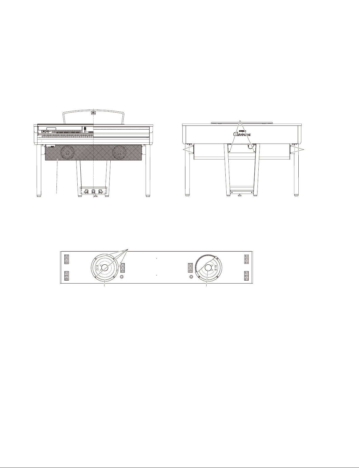
24. Woofer
(Time required : About 3 minutes each)
24-1. Remove the front grille. (Fig. 33)
24-2. Remove the four (4) screws marked [8B]. The woofer
can then be removed. (Fig. 34)
* The left and right woofer each can then be removed in
the same manner.
24.
ウーファー
(所要時間:各約 3 分)
24-1. フロントグリルを外します。(図 33)
24-2.
[8B] のネジ 4 本を外し、ウーファー(L)を外します。
(図34)
※ ウーファー(R)も同様に外すことができます。
<Front view / 前面> <Back view /
[11aD]
Front grille
(フロントグリル)
Speaker Box Assembly
●
(Fig.33)(図 33)
[11aD]:BindHeadScrew(小ネジ+ BIND)5.0x18MFZN2B3
(WF741300)
<Front view / 前面>
[8B]
後面
>
[11aD]
[11aD]
30
Woofer L
(ウーファーL)
[8B]:BindHeadTappingScrew-1(TP#1 + BIND)4.0x14MFZN2B3(WF745800)
(Fig.34)(図 34)
Woofer R
(ウーファーR)
 Loading...