

Page 1

CVP-309PE/CVP-309PM
CVP-309PE / CVP-309PM
SERVICE MANUAL
CVP-309PE CVP-309PM
CONTENTS
SPECIFICATIONS ................................................................... 3
PANEL LAYOUT ...................................................................... 5
DISASSEMBLY PROCEDURE ................................................ 8
LSI PIN DESCRIPTION .......................................................... 22
IC BLOCK DIAGRAM ............................................................. 31
CIRCUIT BOARDS ................................................................. 33
TEST PROGRAM ................................................................... 68
VERSION UPGRADE ............................................................. 75
DATA BACKUP ....................................................................... 78
RESTORING THE FACTORY-PROGRAMMED SETTING .... 82
INITIALIZING INTERNET SETTING ...................................... 84
FACTORY SET ....................................................................... 84
SYSTEM BOOTING FLOWCHART ........................................ 85
MIDI IMPLEMENTATION CHART .......................................... 87
MIDI DATA FORMAT .............................................................. 88
PARTS LIST
BLOCK DIAGRAM
CIRCUIT BOARD LAYOUT & WIRING
OVERALL CIRCUIT DIAGRAM
CL
001727
HAMAMATSU, JAPAN
Copyright (c) Yamaha Corporation. All rights reserved. PDF-K1682 ’04.08
1
Page 2

CVP-309PE/CVP-309PM
p
This manual has been provided for the use of authorized Yamaha Retailers and their service personnel. It has been assumed
that basic service procedures inherent to the industry, and more specifically Yamaha Products, are already known and understood by the users, and have therefore not been restated.
WARNING : Failure to follow appropriate service and safety procedures when servicing this product may result in per-
IMPORTANT : This presentation or sale of this manual to any individual or firm does not constitute authorization certifi-
The data provided is belived to be accurate and applicable to the unit(s) indicated on the cover. The research engineering, and
service departments of Yamaha are continually striving to improve Yamaha products. Modifications are, therefore, inevitable
and changes in specification are subject to change without notice or obligation to retrofit. Should any discrepancy appear to
exist, please contact the distributor’s Service Division.
WARNING : Static discharges can destroy expensive components. Discharge any static electricity your body may have
IMPORTANT : Turn the unit OFF during disassembly and parts replacement. Recheck all work before you apply power
The solder used in the production of this product contains LEAD. In addition, other electrical/electronic and/or plastic (Where
applicable) components may also contain traces of chemicals found by the California Health and Welfare Agency (and possibly
other entities) to cause cancer and/or birth defects or other reproductive harm.
DO NOT PLACE SOLDER, ELECTRICAL/ELECTRONIC OR PLASTIC COMPONENTS IN YOUR MOUTH FOR ANY REASON WHAT
SO EVER!
Avoid prolonged, unprotected contact between solder and your skin! When soldering, do not inhale solder fumes or expose
eyes to solder/flux vapor!
If you come in contact with solder or components located inside the enclosure of this product, wash your hands before handling
food.
IMPORTANT NOTICE
sonal injury, destruction of expensive components and failure of the product to perform as specified. For
these reasons, we advise all Yamaha product owners that all service required should be performed by an
authorized Yamaha Retailer or the appointed service representative.
cation, recognition of any applicable technical capabilities, or establish a principal-agent relationship of
any form.
accumulated by grounding yourself to the ground bus in the unit (heavy gauge black wires connect to
this bus.)
to the unit.
WARNING: CHEMICAL CONTENT NOTICE!
IMPORTANT NOTICE FOR THE UNITED KINGDOM
Connecting the Plug and Cord
IMPORTANT : The wires in this mains lead are coloured in accordance with the following code:
As the colours of the wires in the mains lead of this apparatus may not correspond with the coloured makings identifying the te rminals in your plug
proceed as follows:
The wire which is coloured BLUE must be connected to the terminal which is marked with the letter N or coloured BLACK.
The wire which is coloured BROWN must be connected to the terminal which is marked with the letter L or coloured RED.
Making sure that neither core is connected to the earth terminal of the three pin plug.
BLUE : NEUTRAL
BROWN : LIVE
WARNING
Components having special characteristics are marked and must be replaced with parts having specification equal to those
originally installed.
SAVING DATA
Saving and backing up your data
Be sure to
erform it
The data of the types listed below are lost when you turn off the power to the instrument. Save the data to the USER
tab display, floppy disk, SmartMedia card, or appropriate external media.
• Recorded/Edited Songs
• Created/Edited Styles
• Edited Voices
• Memorized One Touch Settings
• Edited MIDI settings
2
Page 3

CVP-309PE/CVP-309PM
SPECIFICATIONS
Sound Source AWM Dynamic Stereo Sampling
Keyboard Natural Wood Keyboard 88 keys
LCD Display 640 x 480 dots VGA color LCD
Music Score, Lyrics YES
Wallpaper Customize YES
Polyphony (max) 128 + 128
Voice Selection
Mega Voice 10
Regular Voice 338
Voice
Sound Creator YES
Effect Blocks
Effects
Accompaniment Style
Song
Internet Direct Connection External Adapter (via USB to DEVICE)
Memory Device
Effect Types
Vocal Harmony 61 Preset + 10 User
Accompaniment Styles 386
Mega Voice Styles YES
Fingering
Style Creator YES
OTS (One Touch Setting) 4 for Each Style
OTS Link YES
Music Finder
Preset Songs 120
Guide Follow Lights, Any Key
Performance assistant technology YES
Recording
Floppy Disk (2HD, 2DD) External Adapter (via USB to DEVICE)
Hard Disk External Adapter (via USB to DEVICE)
Flash Memory (Internal) 3.3 MB
SmartMedia Slot 1 (Compatible with SmartMedia FAT 12 or 16 format.)
Natural! Voice 38
Sweet! Voice 14
Cool! Voice 19
Live! Voice 22
Organ Flutes! 10
Reverb/Chorus/DSP 8
Microphone 1
Reverb/Chorus/DSP
Master EQ 5 Preset + 2 User
Master Compressor 5 Preset + 5 User
Part EQ 27 Parts
Pro Styles 316
Session Styles 34
Pianist Styles 36
Single Finger, Fingered, Fingered On Bass, Multi Finger,
Preset YES
Edit YES
Guide Lamp YES
Quick Recording, Multi Recording, Step Recording,
Record Channels 16
451 voices + 480 XG Voices
17 Drum/SFX Kits + GM2 + GS
(GS Voices for GS Song playback)
Reverb: 35 Preset + 3 User
Chorus: 31 Preset + 3 User
DSP 1: 183 Preset + 3 User
DSP 2–5: 182 Preset + 10 User
DSP 6: 182 Preset + 10 User
AI Fingered, Full Keyboard, AI Full Keyboard
,
Karao-Key,Vocal CueTIME
Song Editing
3
Page 4

CVP-309PE/CVP-309PM
Tempo
Registration Memory
Others
USB Connection
Other Connectors
Pedals Functions
Amplifiers/Speakers Amplifiers
Dimensions [W x D x H]
(with the Music Rest)
Weight
Optional Accessories
Accessories
Output Impedance
Tempo Range 5–500, Tap Tempo
Metronome YES
Sound
Buttons 8
Regist. Sequence/Freeze YES
Demo/Help YES
Language for Display
Direct Access YES
Piano Button (incl. Piano Lock) YES
Transpose Keyboard/Song/Master
Scale Type 9
USB to HOST (Computer) YES
USB to DEVICE YES (2 terminals)
iAFC
Speakers (16 cm + 5 cm + 3cm(dome)) x 2 +10cm x 2
Headphones HPE-160
Foot Switch FC 4/FC 5
Foot Controller FC 7
USB-FDD Unit UD-FD01
(English, Japanese, German, French, Spanish, Italian)
PHONES x 2, MIDI (THRU, OUT, IN), AUX PEDAL,
VOLUME, SUSTAIN, SOSTENUTO, SOFT, GLIDE,
SONG PLAY/PAUSE, STYLE START/STOP, etc.
1430 mm x 609 mm x 890 mm [57-3/16" x 23" x 35-3/8"]
(1430 mm x 609 mm x 1047 mm) [57-3/16" x 23" x 41-1/4"]
Guide to Yamaha Online Member Product User Registration
"50 greats for the Piano" Music Book, Owner's Manual, Data List
The following items may be included or optional,
depending on your locale:
Floppy Disk Drive, SmartMedia card, Bench
Bell on/off, Human Voices
(5 Languages)
6 Languages
AUX IN (L/L+R, R), AUX OUT (L/L+R, R),
AUX OUT (LEVEL FIXED) (L, R),
MIC (INPUT VOLUME, MIC./LINE IN),
OPTICAL OUT, VIDEO OUT
YES
60 W x 2 + 20 W x 2
88 kg (194 lbs)
PHONES: 33Ω (Recommend)
OUTPUT (L/L+R,R): 600Ω
AUX OUT (L,R) (LEVEL FIXED): 600Ω
4
Page 5

PANEL LAYOUT
CVP-309PE/CVP-309PM
q [PHONES] jacks
w • [MIC./LINE IN] jack
• [INPUT VOLUME] dial
e [OPTICAL OUT] jack
r [AUX OUT] jacks
t [AUX IN] jacks
y [VIDEO OUT] jack
u [AUX PEDAL] jack
i [MIDI] terminals
o-1 [USB TO HOST] terminal
o-2 [USB TO DEVICE] terminal
5
Page 6
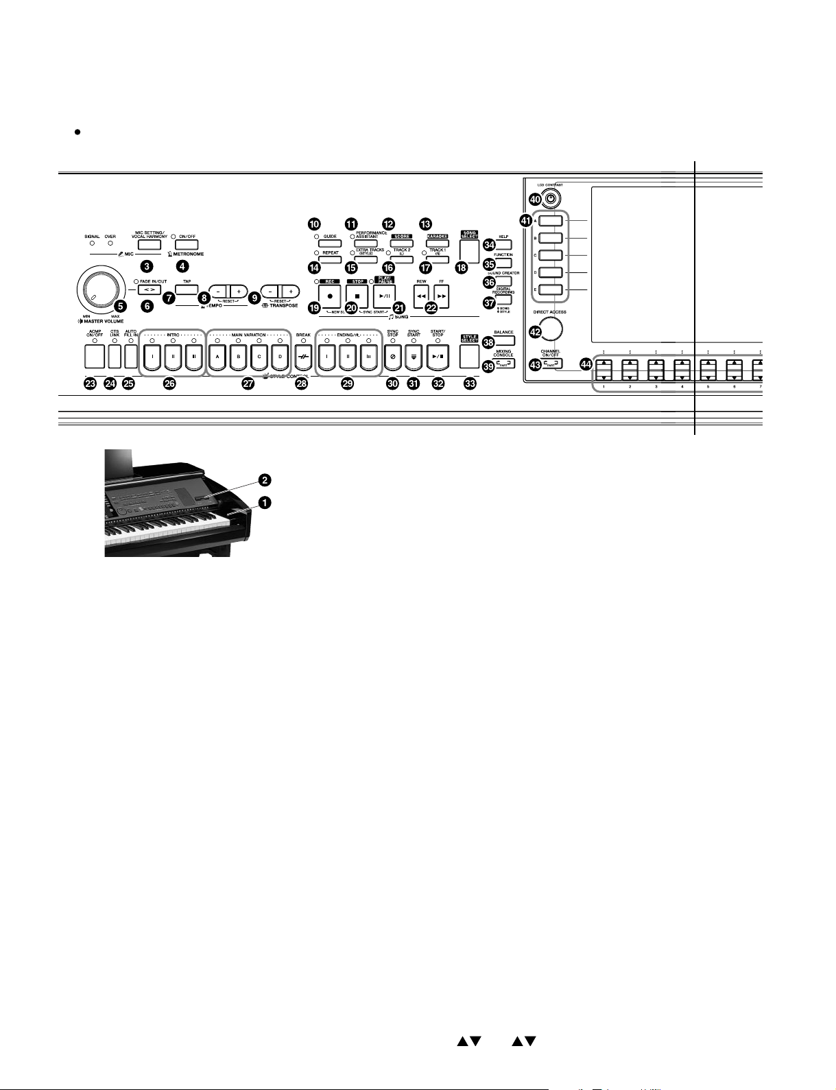
CVP-309PE/CVP-309PM
Front Panel
A
A'
q [POWER] switch
w SmartMedia slot
MIC.
e [MIC SETTING / VOCAL HARMONY] button
METRONOME
r [ON/OFF] button
VOLUME
t [MASTER VOLUME] dial
y [FADE IN / OUT] button
TEMPO
u [TAP] button
i [
-
] [ + ] buttons
TRANSPOSE
o [
-
] [ + ] buttons
SONG
!0 [GUIDE] button
!1 [PERFORMANCE ASSISTANT] button
!2 [SCORE] button
!3 [KARAOKE] button
!4 [REPEAT] button
!5 [EXTRA TRACKS (STYLE)] button
!6 [TRACK 2 (L)] button
!7 [TRACK 1 (R)] button
!8 [SONG SELECT] button
!9 [REC] button
6
@0 [STOP] button
@1 [PLAY / PAUSE] button
@2 [REW] / [FF] buttons
STYLE CONTROL
@3 [ACMP ON / OFF] button
@4 [OTS LINK] button
@5 [AUTO FILL IN] button
@6 INTRO [I] / [II] / [III] buttons
@7 MAIN VARIATION [A] / [B] / [C] / [D] buttons
@8 [BREAK] button
@9 ENDING/rit. [I]/[II]/[III] buttons
#0 [SYNC STOP] button
#1 [SYNC START] button
#2 [START/STOP] button
#3 [STYLE SELECT] button
#4 [HELP] button
#5 [FUNCTION] button
#6 [SOUND CREATOR] button
#7 [DIGITAL RECORDING] button
#8 [BALANCE] button
#9 [MIXING CONSOLE] button
$0 [LCD CONTRAST] knob
$1 [A]–[J] buttons
$2 [DIRECT ACCESS] button
$3 [CHANNEL ON/OFF] button
$4 [1
]–[8
] buttons
Page 7
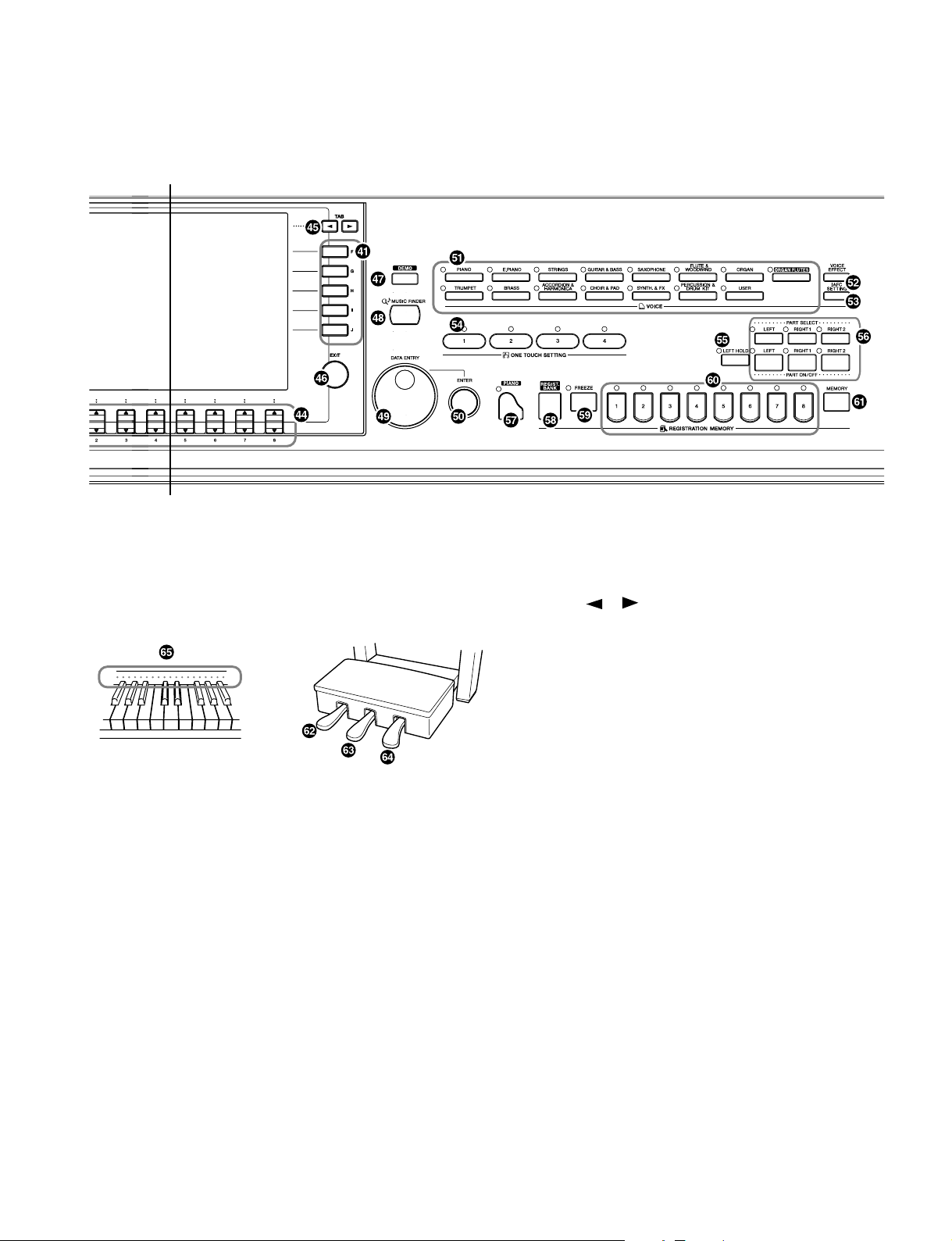
CVP-309PE/CVP-309PM
A
A'
$5 TAB [ ][
$6 [EXIT] button
$7 [DEMO] button
$8 [MUSIC FINDER] button
$9 [DATA ENTRY] dial
%0 [ENTER] button
VOICE
%1 VOICE buttons
%2 [VOICE EFFECT] button
%3 [ iAFC SETTING] button
ONE TOUCH SETTING
%4 [ 1 ] – [ 4 ] buttons
%5 [LEFT HOLD] button
PART
%6 PART buttons
PIANO Setting
%7 [PIANO] button
REGISTRATION MEMORY
%8 [REGIST. BANK] button
%9 [FREEZE] button
^0 [ 1 ] - [ 8 ] buttons
^1 [MEMORY] button
Pedals
^2 Left pedal
^3 Sostenuto pedal
^4 Damper pedal
] buttons
^5 Keyboard guide lamps
7
Page 8

CVP-309PE/CVP-309PM
■ DISASSEMBLY PROCEDURE
1. Headphone Hanger
(Time required : About 1 minute)
Remove the two (2) screws marked [17b]. The
headphone hanger can then be removed. (Fig. 1)
2. Mic. & Phones Unit, MIC and HP Circuit Boards
2-1. Remove the four (4) screws mark ed [77]. The mic . &
phones unit can then be removed. (Fig. 1)
2-2. MIC Circuit Board
2-2-1. Remove the input volume knob, the hexagonal nut
marked [N1] and the washer marked [W1]. (Fig. 2)
2-2-2. Remove the hexagonal nut marked [40A] and the
washer marked [50A]. The MIC circuit board can then
be removed. (Fig. 2)
*
When installing the INPUT VOLUME knob, set it to the
VOL. MIN position, that is, align the bar on the knob with
the point on the case as shown in the figure. (Fig. 2)
2-3. HP Circuit Board
Remove the two (2) hexagonal nuts mark ed [40B] and
the two (2) washers marked [50B]. The HP circuit
board can then be removed. (Fig. 2)
(Time required : About 3 minutes each)
Headphone hanger
Mic. & phones unit
[17b]
[77]
[17b]: Truss Head Screw 4.0x10 MFZN2BL (VT196400)
[77]: Bind Head Tapping Screw-1 3.5x14 MFZN2BL (EP030250)
[84]: Truss Head Screw 4.0x10 MFZN2BL (VT196400)
(Fig. 1)
FDD unit
[84]
● Mic. & Phones Unit
<Front view>
[50B]
Knob
<Side view>
[50A]
Knob
3. Floppy Disk Drive
(Time required : About 3 minutes)
3-1. Disconnect the USB connector.
3-2. Remove the four (4) screws marked [84]. The FDD
unit can then be removed. (Fig. 1)
3-3. Remove the USB-3.5FDD attached by the double-
sided tapes from the FDD holder assembly. (Fig. 3)
* Note that once you remove the double-sided tape (FDD
[50B]
[40B][40A]
HP
cushion), you cannot use it again. In the replacing of
USB-3.5 FDD, use new double-sided tapes (FDD
cushions) to install the FDD.
● FDD Unit
USB-3.5FDD
[N1] [W1]
[40]: Hexagonal Nut 12.0x14x2 MFZN2BL (VB508600)
[50]: Washer (VJ869400)
[N1]: Hexagonal Nut
[W1]: Washer
(Fig. 2)
8
MIC
Double-sided Tape
(FDD cushion)
FDD holder assembly
(Fig. 3)
Page 9

CVP-309PE/CVP-309PM
4. Music Rest Assembly
(Time required : About 1 minute)
Remove the two (2) screws marked [13] from both
sides of the assembly. The music rest assembly can
then be removed. (Fig. 4)
5. Top Board Assembly
(Time required : About 1 minute)
5-1. Open the key cover a little so that the screws marked
[80] can be seen.
5-2. Remove the screw marked [80] from both sides of the
assembly. Mo ve the top board assembly rearward, and
it can then be removed by lifting up. (Fig. 5)
[80]
Top board assembly
Music rest assembly
[13]
[13]: Bind Head Tapping Screw-1 3.5x16 MFZN2BL (EP030260)
(Fig. 4)
Top board assembly
[80]
(Fig. 5-1)
6. Circuit Boards and Assembles (Main
Unit Section)
(Time required: About 5 minutes each)
6-1. Remove the top board assembly. (See procedure 5)
6-2. Slide the key cover rearward, remove its guide pin of
the back key cover from the opening for the arm. Then
the back key cover can be opened. (Fig. 6)
Back key cover
Guide pin
Key cover
[80]: Cap Screw 3.0x8 MFZN2BL (VP575300)
(Fig. 5)
Arm
Back key cover
Opening for the arm
(Fig. 6)
9
Page 10

CVP-309PE/CVP-309PM
6-3. Each circuit board and assembly can be removed by removing its fixing screws as listed below.
Circuit board and Assembly Ref. No. Screw QTY Fig.
PK Connector 70A Bind Head Tapping Screw-1 3.5x12 MFZN2Y (EP030240) 2 7
PJK Circuit Board 23c Bind Head Tapping Screw-B 3.0x8 MFZN2BL (EP600190) 2 7
DM2-A Circuit Board 76A Bind Head Tapping Screw-B 3.0x8 MFZN2Y (EP600250) 6 7
TG1 Circuit Board 82A Bind Head Screw 3.0x8 MFZN2Y (VD976600) 2 7
TG2 Circuit Board 76B Bind Head Tapping Screw-B 3.0x8 MFZN2Y (EP600250) 2 7
DAC2A Circuit Board 15e Bind Head Tapping Screw-B 3.0x8 MFZN2Y (EP600250) 4 7
TN Circuit Board 28c Bind Head Tapping Screw-B 3.0x8 MFZN2Y (EP600250) 4 7
EQ Circuit Board 79A Bind Head Tapping Screw-1 3.5x20 MFZN2Y (EP030470) 4 7
HUB Circuit Board 79B Bind Head Tapping Screw-1 3.5x20 MFZN2Y (EP030470) 4 7
NET1 Circuit Board 79C Bind Head Tapping Screw-1 3.5x20 MFZN2Y (EP030470) 4 7
NETWORK Circuit Board 79D Bind Head Tapping Screw-1 3.5x20 MFZN2Y (EP030470) 4 7
Jack Assembly
MA Cover (U.S.A. model only) 109A Bind Head Tapping Screw-1 3.5x12 MFZN2Y (EP030240) 2 7
MA160S Assembly 70C Bind Head Tapping Screw-1 3.5x12 MFZN2Y (EP030240) 2 7
MAF Assembly 70D Bind Head Tapping Screw-1 3.5x12 MFZN2Y (EP030240) 2 7
FU Cover (U.S.A. model only) 109B Bind Head Tapping Screw-1 3.5x12 MFZN2Y (EP030240) 2 7
FU120LB Assembly 70E Bind Head Tapping Screw-1 3.5x12 MFZN2Y (EP030240) 2 7
Pow er Transformer
MIC (AFC) Circuit Board 79E Bind Head Tapping Screw-1 3.5x20 MFZN2Y (EP030470) 3 7
Wire Rail 76C Bind Head Tapping Screw-B 3.0x8 MFZN2Y (EP600250) 6 7
CN Circuit Board 79F Bind Head Tapping Screw-1 3.5x20 MFZN2Y (EP030470) 4 7
118 Truss Head Tapping Screw-1 3.5x14 MFZN2Y (EN630230) 1 7
70B Bind Head Tapping Screw-1 3.5x12 MFZN2Y (EP030240) 3 7
78 Bind Head Screw 4.0x12 MFZN2BL (VB132700) 4 7
85 Flat Wsher 4.0x12x1.0 MFZN2Y (VK287600) 4 7
DAC2A TN
[15e] x 4
[70B] x 3
[118]
[28c] x 4
[79A] x 4
EQ
HUB
TG2
PK connector
[70A]
[23c]
TG1
PJK
[70A]
●
DIP switch
English
OFF
DM2-A
Japanese
SW3: OFF
SW2: OFF
SW1: ON
ON
[79C] x 4
DM2-A circuit board has internal DIP switches for switching
the model (SW1 & SW2) and for switching the display in
Japanese or in English (SW3).
DIP switch (SW3) ON OFF
LCD display language Japanese English
VIDEO OUT NTSC/(PAL)
Demonstration music For Japan For other than Japan
Access home page to Server in Japan Server in U.S.A.
NET1
MA cover
[109A] x 2
MA160S assembly
[70C] x 2
MAF assembly
[70D] x 2
FU cover
[109B] x 2
FU120LB
assembly
[70E] x 2
10
[79B] x 4
Jack assembly
Back key cover
[76B] x 2
[82A] x 2
[76A] x 6
Wire rail
[76C] x 6
[79D] x 4
NETWORK
(Fig. 7)
[79F] x 4
[79E] x 3
CN
Power transformer
MIC (AFC)
[78] x 4
[85] x 4
Page 11

[7A] [7B] [7A][7B]
[4B]
[4B]
[4A]
[6B], [5B]
[4A][6A], [5A]
AJACK
DJACK
DJACK
AJACK
7. AJACK and DJACK Circuit Boards
(Time required : About 10 minutes each)
7-1. Remove the top board assembly. (See procedure 5)
7-2. Open the back key cover. (See procedure 6-2)
7-3. Remove the jack assembly. (See procedure 6-3)
7-4. DJACK Circuit Board
Remove the two (2) screws marked [7A], four (4)
screws marked [4A], the heagonal nut marked [6A]
and the washer marked [5A]. The DJ A CK circuit board
can then be removed. (Fig. 8)
7-5. AJACK Circuit Board
Remove the two (2) screws marked [7B], two (2)
screws marked [4B], the four (4) heagonal nuts marked
[6B] and the four (4) washers marked [5B]. The
AJACK circuit board can then be removed. (Fig. 8)
8. White Key, Black Key
(Time required : About 10 minutes)
8-1. Remove the top board assembly. (See procedure 5)
8-2. Open the back key cover. (See procedure 6-2)
8-3. Remove the wire rail. (See procedure 6-3)
8-4. Remove the ten (10) screws marked [70F]. The MT
angle assembly and angle can then be removed.
(Fig. 9)
8-5. Remove the nine (9) screws marked [72] and the two
(2) screws marked [73], move the keyboard assembly
rearward. (Fig. 9)
CVP-309PE/CVP-309PM
● Jack Unit
[4]: Bind Head Tapping Screw-B 3.0x8 MFZN2BL (EP600190)
[5]: Washer (VJ869400)
[6]: Hexagonal Nut 12.0x14x2 MFZN2BL (VB508600)
[7]: Bind Head Tapping Screw-B 3.0x8 MFZN2Y (EP600250)
(Fig. 8)
MT angle assembly Keyboard assembly Wire rail
[72] [72] [72]
[73] [73]
Back key cover
Angle
[72] [72]
[70F]: Bind Head Tapping Screw-1 3.5x12 MFZN2Y (EP030240)
[72]: Pan Head Screw PW5.0x25 MFZN2Y (VV040700)
[73]: Bind Head Tapping Screw-1 4.0x14 MFZN2Y (EP040230)
[70F][70F][70F] [70F]
[70F]
(Fig. 9)
11
Page 12

CVP-309PE/CVP-309PM
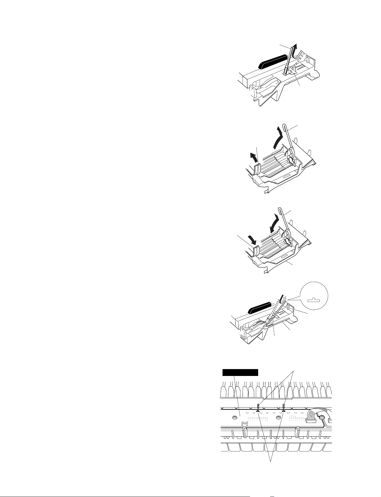
8-6. White key
In order to release the white key from the stopper , insert
a thin plate between the white keys (gap in the direction
indicated by the triangle mark, near the fulcrum of the
key), press down the stopper marked [A] and move
the white key forward. Then the white key being
released from the stopper lifts up. (Fig. 10, 11, 12)
* Use special care not to move the white key forward so
much as to cause damage to the key spring.
8-7. Hold the key cover assembly under your arm. In this
state, move the white key rearward a little. Then the
white key can be removed. (Fig. 13)
8-8. Black key
The black key can be removed after the white ke ys on
either side have been removed.
If the illustration of a camera is clicked, an animation will flow.
This animation shows CVP-303.
Thin metal plate etc
(Fig. 10)
White key
[A]
(Fig. 11)
Triangle mark
Spring
* This photo shows CVP-303.
(The process is the same for CVP-309 as well.)
Back key cover
Front key cover
* This photo shows CVP-303.
(The process is the same for CVP-309 as well.)
8-9. Assembling the White Key (Black Key)
After a key has been fit to part [C] and key guide,
make sure that the spring is fixed to the key and then
press down part [B] of the key. (Fig. 14)
(Fig. 12)
(Fig. 13)
* This photo shows CVP-303.
(The process is the same for CVP-309 as well.)
* This photo shows CVP-303.
(The process is the same for CVP-309 as well.)
White key [B]
12
If the illustration of a camera is clicked, an animation will flow.
This animation shows CVP-303.
[C]
Key guide
(Fig. 14)
Spring
Page 13

9. Key Cover Assembly
(Time required: About 5 minutes)
9-1. Remove the top board assembly. (See procedure 5)
9-2. Open the back key cover. (See procedure 6-2)
9-3. Remove the screw marked [82B], pull off the rod from
the spring holder and remove the spring R. (Fig. 15)
* Remove the spring L in the same manner.
9-4. Remove the four (4) screws marked [3]. (Fig. 15)
9-5. Using the tip end of the panel as the fulcrum, pull up
the key cover assembly to remove it. (Fig. 16)
Spring L
[82B]
CVP-309PE/CVP-309PM
Spring R
Rod
[3]
Back key cover
[3]: Bind Head Tapping Screw-B 3.0x10 MFZN2Y (EP600220)
[82B]: Bind Head Screw 3.0x8 MFZN2Y (VD976600)
(Fig. 15)
Installation of Key Cover
[3]
Fit the sash of the key cover ov er the tip end of the panel and install the ke y co ver, using care for the balance between right and
left. When the key cover is installed properly, lugs of the panel (CP holders) at 6 locations should fit in the groove in the key
cover . If there is a lug (CP holder) that is not fitted in the groo v e, push around it so that it will fit in the groo ve. (Fig. 16, Fig . 17)
● Key Cover & Panel Assembly
<Side view>
Key cover
Key cover
Panel assembly
CP holder
Groove
(Fig. 16)
Panel assembly
Sash
13
Page 14

CVP-309PE/CVP-309PM
10. Circuit Boards and Assembles (Panel Assembly Section)
(Time required: About 10 minutes each)
10-1. Remove the top board assembly. (See procedure 5)
10-2. Open the back key cover. (See procedure 6-2)
10-3. Remove the key cover assembly. (See procedure 9)
10-4. Put cloth or the like between the panel assembly and keyboard to pre vent the panel assembly from being distorted .
10-5. Remove the screws listed below. Then the circuit board and assembly can be removed.
Circuit board and Assembly Ref. No. Screw QTY Fig.
Speaker (L or R) 80c Bind Head Tapping Screw-B 3.0x8 MFZN2BL (EP600190) 2 17
AFC Capacitor Mic (L or R) *1 80e
SM *2 625 Bind Head Tapping Screw-B 3.0x6 MFZN2BL (EP600230) 2 17
INV 620A Bind Head Tapping Screw-B 3.0x8 MFZN2Y (EP600250) 4 17
LCD 620B Bind Head Tapping Screw-B 3.0x8 MFZN2Y (EP600250) 4 17
MV1
620C Bind Head Tapping Screw-B 3.0x8 MFZN2Y (EP600250) 4 17
ENC
PNL (PNL1 *3, PNL2) + PNC *4
+ PNR (PNR1 *5, PNR2, PNR3)
*1 For removal of the AFC capacitor mic on the speaker box assembly, refer to procedure 22.
*2 Before replacing the SM circuit board, check to ensure that Smart Media is not inserted.
*3 To remove the PNL1 circuit board, be sure to remove the MV1 circuit board first.
*4 The PNL1 circuit board (CN103) and PNC circuit board (CN103) are connected directly using connectors.
When removing the PNL1 circuit board and PNC circuit board, use care not to cause damage to the connector (CN103).
*5 To remove the PNR1 circuit board, be sure to remove the ENC circuit board first.
620D Bind Head Tapping Screw-B 3.0x8 MFZN2Y (EP600250) 4 17
620E Bind Head Tapping Screw-B 3.0x8 MFZN2Y (EP600250) 70 17
Plastic Rivet P3065B (V9240700) First lot
Plastic Rivet P3055 NIX (WA388200) Second lot ~
Knob (MASTER VOLUME) 1 17
N2 Hexagonal Nut 1 17
W2 Washer 117
Encoder Knob (DATA ENTRY) 1 17
217
● Panel Assembly
<Top view>
Knob
Encoder knob
<Bottom view>
PNL2 MV1 PNL1 PNC SMPNR1 PNR2
[620E] x 3
CP holder CP holder CP holder CP holder
[620C] x 4 [620E] x 26 [620E] x 11
[N2]
[W2]
CN103
PNL1
MV1
[620B] x 4
LCD
CN103
PNC
(Fig. 17)
ENC
[620E] x 4
PNR3
[620D] x 4
INV
[620A] x 4
[620E] x 23
[80c]
[80e]
[620E] x 3 [625] x 2
Speaker R
capacitor mic R
AFC
14
Page 15

CVP-309PE/CVP-309PM
Turning axle assembly L
Turning axle assembly R
Back key cover
[83]
[83]
[83]
[83]
Arm R
Damper
Panel assembly
Spring L Spring R
11. Panel Assembly
(Time required: About 10 minutes)
11-1. Remove the top board assembly. (See procedure 5)
11-2. Open the back key cover. (See procedure 6-2)
11-3. Remove the key cover assembly. (See procedure 9)
11-4. Put cloth or the like between the panel assembly and
keyboard.
11-5. Remove the four (4) screws marked [83] and then
remove the turning axle assembly R from the panel
assembly. (Fig. 18)
* When installing the turning axle assembly R, carefully
check for the direction of the damper (turning axle) on
the side of the arm assembly R. The turning axle
assembly R should be installed in such direction that
letters ("TH") stamped on the damper (turning axle) is
upside down. Installation otherwise will damage the
damper.
11-6. Remove the turning axle assembly L in the same
manner. (Fig. 18)
* Be sure to remove the turning axle assembly R first.
11-7. Remove the panel assembly. (Fig. 18)
12. Key Cover & Panel Assembly
(Time required: About 10 minutes)
12-1. Remove the top board assembly. (See procedure 5)
12-2. Open the back key cover. (See procedure 6-2)
12-3. Remove the spring L and R. (See procedure 9-3)
12-4. Put cloth or the like between the panel assembly and
keyboard.
12-5. Remove the turning axle assembly R from the panel
assembly. (See procedure 11-5)
12-6. Remove the turning axle assembly L from the panel
assembly. (See procedure 11-6)
12-7. Remove the key cover and panel assembly. (Fig. 18)
[83]: Bind Head Tapping Screw-B 3.0x10 MFZN2Y (EP600220)
(Fig. 18)
15
Page 16

CVP-309PE/CVP-309PM
13. End Block Assembly (L, R)
(Time required : About 15 minutes)
13-1. Remove the top board assembly. (See procedure 5)
13-2. Open the back key cover. (See procedure 6-2)
13-3. Remove the key cover and panel assembly.
(See procedure 12)
13-4. Remove the screw mark ed [74] and the washer marked
[86]. The end block assembly can then be removed.
(Fig. 19)
* The left and right end block assembly can then be
removed in the same manner.
MT angle assembly
Angle
14. Keyboard Assembly
(Time required : About 20 minutes)
14-1. Remove the top board assembly. (See procedure 5)
14-2. Open the back key cover. (See procedure 6-2)
14-3. Remove the key cover and panel assembly.
(See procedure 12)
14-4. Remove the end block assembly L and R.
(See procedure 13)
14-5. Remove the wire rail. (See procedure 6-3)
14-6. Remove the MT angle assembly and angle.
(See procedure 8-4)
14-7. Remove the keyboard assembly. (See procedure 8-5)
[CN002]
NET1
[CN12]
MIC (AFC)
MAF
[CN3]
[74], [86]End block assembly L [74], [86] End block assembly R
[81]
[74]: Bind Head Tapping Screw-B 4.0x20 MFZN2BL (VS205900)
[81]: Bind Head Screw SP 5.0x30 MFZN2BL (VQ635300)
[86]: Flat Washer 4.0x8 0.8 MFZN2Y (VA226100)
Keyboard assembly
15. Power Switch Assembly
(Time required : About 20 minutes)
15-1. Remove the top board assembly. (See procedure 5)
15-2. Open the back key cover. (See procedure 6-2)
15-3. Remove the key cover and panel assembly.
(See procedure 12)
15-4. Remove the end block assembly R.
(See procedure 13)
15-5. Remove the two (2) screws marked [8]. The power
switch assembly can then be removed from the end
block assembly R. (Fig. 20)
15-6. Remove the two (2) screws marked [6C]. The power
switch assembly can then be removed from the angle.
(Fig. 20)
(Fig. 19)
[81]
● End Block Assembly R
<Side view>
[8]
[6C]: Bind Head Tapping Screw-B 3.0x6 MFZN2BL (EP600230)
[8]: Bind Head Tapping Screw-1 3.5x10 MFZN2BL (EP030320)
(Fig. 20)
Angle
[6C]
Power switch assembly
16
Page 17

CVP-309PE/CVP-309PM
Front rail assembly
Arm assembly L
FDD unit
Arm assembly R
Back top board assembly
[71A]
[71C]
[71C]
[71C]
[71A]
[71A]
[71A]
[71B]
[71B]
[71B]
[71B]
16. PL Circuit Board
(Time required : About 25 minutes)
16-1. Remove the top board assembly. (See procedure 5)
16-2. Open the back key cover. (See procedure 6-2)
16-3. Remove the key cover and panel assembly.
(See procedure 12)
16-4. Remove the end block assembly L and R.
(See procedure 13)
16-5. Remove the keyboard assembly. (See procedure 14)
16-6. Remove the screw marked [6D]. The PL circuit board
can then be removed. (Fig. 21)
17. Front Rail Assembly
(Time required : About 25 minutes)
17-1. Remove the FDD unit. (See procedure 3)
17-2. Remove the top board assembly. (See procedure 5)
17-3. Open the back key cover. (See procedure 6-2)
17-4. Remove the key cover and panel assembly.
(See procedure 12)
17-5. Remove the end block assembly L and R.
(See procedure 13)
17-6. Remove the keyboard assembly. (See procedure 14)
17-7. Remove the two (2) screws marked [75A] from both
sides of the assembly. (Fig. 21)
17-8. Remove the seven (7) scre ws mark ed [71A]. The front
rail assembly can then be removed. (Fig. 23)
PL
Front rail assembly
[6D]
[6D]: Bind Head Tapping Screw-1 3.5x12 MFZN2BL (EP030340)
[75A]: Bind Head T apping Screw-1 3.5x16 MFZN2Y (EP030190)
Arm assembly L
[75A]
(Fig. 21)
Back top board assembly
Arm assembly L
[75B]
18. Back Top Board Assembly
(Time required : About 10 minutes)
18-1. Remove the top board assembly. (See procedure 5)
18-2. Open the back key cover. (See procedure 6-2)
18-3. Remove the MAF assembly. (See procedure 6-3)
(This is because the MAF assembly is in the way when
removing the screw on the right side of the back top
board assembly .)
<Bottom view>
[75B]: Bind Head T apping Screw-1 3.5x16 MFZN2Y (EP030190)
(Fig. 22)
18-4. Remove the three (3) screws mark ed [75B] from both
sides of the assembly. (Fig. 22)
18-5. Remove the eight (8) screws marked [71B]. The bac k
top board assembly can then be removed. (Fig. 23)
[71]: Truss Head Tapping Screw-1 3.5x25 MFZN2BL (EN630190)
(Fig. 23)
17
Page 18

CVP-309PE/CVP-309PM
19. Arm Assembly (L, R)
(Time required : About 40 minutes)
19-1. Remove the top board assembly. (See procedure 5)
19-2. Open the back key cover. (See procedure 6-2)
19-3. Remove the key cover and panel assembly.
(See procedure 12)
19-4. Remove the end block assembly L and R.
(See procedure 13)
19-5. Remove the keyboard assembly. (See procedure 14)
19-6. Remove the two (2) screws marked [75A], the three
(3) screws marked [75B] and the five (5) screws
marked [71C]. The arm assembly L can then be
removed. (Fig. 21, 22, 23)
* The arm assembly R can then be removed in the same
manner.
* To remove the arm assembly R, be sure to remove the
MAF assembly first.
(This is because the MAF assembly is in the way when
removing the screw on the right side of the back top
board assembly.)
20. Pedal Box Assembly, Pedal Assembly
(Time required : About 10 minutes)
20-1. Remove the cap from the rear leg L, and disconnect
the PK-LF cable. (fig. 24)
20-2. Remove the two (2) screws marked [11a]. The pedal
box assembly can then be removed. (Fig. 24)
20-3. Remove the eight (8) screws marked [7C] and the
screw marked [10A]. The pedal assembly can then be
removed. (Fig. 25)
20-4. Remove the three (3) screws marked [9A]. The pedal
box can then be removed. (Fig. 25)
21. Front and Rear Leg Assembly
(Time required : About 15 minutes)
21-1. Remove the FDD unit. (See procedure 3)
21-2. Remove the pedal box assembly. (See procedure 20)
21-3. With a soft cloth like a blanket placed on the floor.
Rest the main unit against the wall gently so that the
keyboard side is faced toward the bottom. (Fig. 26)
* For safety, this work should be done by two persons.
21-4. Remove the four (4) screws marked [11a]. The front
leg assembly can then be removed. (Fig. 27)
* The left and right front leg assembly each can then be
removed in the same manner.
21-5. Remove the four (4) screws marked [11a]. The rear
leg assembly can then be removed. (Fig. 28)
Cap
Rear leg L
PK-LF cable
Pedal box assembly
[11a]
[11a]: Bind Head Screw SP 5.0x18 MFZN2BL (V8694700)
(Fig. 24)
[11a]
Pedal assembly
[7C]
[9A]
[11a]
Pedal box
[7C]
[10A]
[9A]
[7C]: Bind Head Tapping Screw-1 4.0x14 MFZN2Y (EP040230)
[9A]: Truss Head Tapping Screw-B 4.0x20 MFZN2BL (V2173700)
[10A]: Truss Head Tapping Screw-1 3.5x14 MFZN2Y (EN630230)
(Fig. 25)
(Fig. 26)
[11a]
[11a]
[11a]
Front leg assembly R
[11a]: Bind Head Screw SP 5.0x18 MFZN2BL (V8694700)
18
[11a]
(Fig. 27)
Front leg assembly R
Rear leg assembly
[11a]: Bind Head Screw SP 5.0x18 MFZN2BL (V8694700)
(Fig. 28)
Page 19

CVP-309PE/CVP-309PM
22. Woofer, Tweeter, AFC Speaker, AFC
Capacitor Mic
(Time required : About 3 minutes each)
22-1. Remove the front grille. (Fig. 29)
22-2. Remove the four (4) screws marked [10B]. The woofer
can then be removed. (Fig. 30)
* The left and right woofer each can then be removed in
the same manner.
22-3. Remove the four (4) screws marked [10C]. The tweeter
can then be removed. (Fig. 30)
* The left and right tweeter each can then be removed
in the same manner.
22-4. Remove the two (2) screws marked [9B]. The MIC
unit can then be removed. (Fig. 30)
22-5. Remove the two (2) plastic rivets marked [14e]. The
AFC capacitor mic can then be removed. (Fig. 30)
* The left and right AFC capacitor mic each can then be
removed in the same manner.
* For removal of the AFC capacitor mic in panel
assembly, refer to procedure 10.
22-6. Remove the rear grille. (Fig. 29)
22-7. Remove the four (4) screws marked [9C]. The AFC
speaker can then be removed. (Fig. 30-1)
* The left and right AFC speaker each can then be
removed in the same manner.
23. Speaker Box Assembly
(Time required : About 20 minutes)
23-1. Remove the FDD unit. (See procedure 3)
23-2. Remove the top board assembly. (See procedure 5)
23-3. Open the back key cover. (See procedure 6-2)
23-4. Remove the wire rail. (See procedure 6-3)
23-5. Remove the eight (8) screws marked [81]. (Fig. 19)
23-6. Disconnect the SP cable from the connector marked
[CN002] located on the NET1 circuit board, the
connector marked [CN3] located on the MAF circuit
board and the connector marked [CN12] located on
the MIC (AFC) circuit board. (Fig. 19)
23-7. With a soft cloth like a blanket placed on the floor.
Rest the main unit against the wall gently so that the
keyboard side is faced toward the bottom. (Fig. 26)
* For safety, this work should be done by two persons.
23-8. Remove the six (6) screws marked [11a]. The speak er
box assembly can then be removed. (Fig. 29)
<Front view> <Back view>
[11a]
Front grille
● Speaker Box Assembly
[11a]: Bind Head Screw SP 5.0x18 MFZN2BL (V8694700)
AFC capacitor mic L
(Fig. 29)
<Front view>
[14e]
[10C]
[9B]
MIC unit L
[10B]
[11a]
[11a]
Rear grille L
MIC unit R
Tweeter L
Woofer L
[9]: Bind Head Tapping Screw-1 3.5x12 MFZN2BL (EP030340)
[10]: Bind Head Tapping Screw-1 4.0x14 MFZN2BL (VR804500)
[14e]: Plastic Rivet P3065B (V9240700) First lot
Plastic Rivet P3055 NIX (WA388200) Second lot ~
(Fig. 30)
Woofer R Tweeter R
19
Page 20

CVP-309PE/CVP-309PM
● Speaker Box Assembly
<Back view>
AFC speaker R
[9]: Bind Head Tapping Screw-1 3.5x12 MFZN2BL (EP030340)
24. Disassembling the Keyboard
* After inserting a round stick (Rod: TX000670) between
the frame and the keys, remove the circuit boards.
(Fig. 31)
AFC speaker L
[9C]
(Fig. 30-1)
24-1. NL2_SW L Circuit Board
Remove the five (5) screws marked [260A] and the
screw marked [262A]. The NL2_SW L circuit board
can then be removed. (Fig. 32)
24-2. NL2_SW M Circuit Board
Remove the four (4) screws marked [260B], the scre w
marked [262A] and the screw marked [262B]. The
NL2_SW M circuit board can then be removed.
(Fig. 32)
24-3. NL2_SW H Circuit Board
Remove the five (5) screws marked [260C] and the
screw marked [262B]. The NL2_SW H circuit board
can then be removed. (Fig. 32)
*
Keys can be removed without removing the circuit
boards.
*
After removing the NL2_SW L, NL2_SW M and NL2_SW H
circuit boards, and the rubbers can then be removed.
24-4. Rubber contact
Remove the NL2_SW circuit board for the involved
key. The rubber contacts can then be removed.
(Fig. 33, 34)
NL2 SW H
Round stick
(Rod: TX000670)
(Fig. 31)
NL2 SW H NL2 SW M
[260C] [260B] [260A][262B] [262A]
[260]: Bind Head Tapping Screw-P 3.0x10 MFZN2Y (EP600270) or
Bind Head Tapping Screw-P 3.0x10 MFZN2 (VT413400)
[262]: PW Head Tapping Screw-P 3.0x10⁻¹⁰ ZMC2Y (V8833200)
(Fig. 32)
Rubber contact
Rubber contact
NL2 SW L
24-5. White Key (Black Key)
See procedure 8-6
20
(Fig. 33) (Fig. 34)
Page 21
CVP-309PE/CVP-309PM
24-6. Hammer, White Key
After a key has been removed, push a ke y spring do wn
once to take it out of the hook. (Fig. 35)
Place the keyboard assembly upside-down and peel
the stopper away. The hammer of the white key can
then be removed. (Fig. 36)
* The hammer of the black key can then be removed in
the same manner.
25. Assembling the Keyboard
25-1. Hammer, White Key (Hammer, Black Key)
Place the keyboard assembly upside-down, insert a
hammer assembly into the frame, and put the stopper
(L88_W) on. (Fig. 37)
* There are four (4) kinds of hammers that differ in
weight.
25-2. Spring
Place the keyboard assembly rightside up. Fix key
springs on the frame by setting one at each slit and
pushing down once on each key spring. (Fig. 38)
* Be careful of the direction of the spring.
25-3. White Key (Black Key)
See procedure 8-9
Spring
Hook
(Fig. 35)
Hammer, white ke y
Stopper (L88_W)
(Fig. 36)
Hammer, white ke y
Stopper (L88_W)
Frame
(Fig. 37)
Up
25-4. NL2_SW L Circuit Board
Tighten the five (5) screws marked [260A] and the
screw marked [262A] to fix the NL2_SW L circuit
board. (Fig. 32)
25-5. NL2_SW M Circuit Board
Tighten the four (4) screws mark ed [260B], the scre w
marked [262A] and the screw marked [262B] to fix
the NL2_SW M circuit board. (Fig. 32)
* When installing the circuit boards, set it under hooks
to align the triangle marks of the circuit board and
projection parts of the frame as shown in figure 39.
25-6. NL2_SW H Circuit Board
Tighten the five (5) screws marked [260C] and the
screw marked [262B] to fix the NL2_SW H circuit
board. (Fig. 32)
Spring
Frame
Hook
(Fig. 38)
Hook
NL2 SW M
Triangle mark
(Fig. 39)
21
Page 22

CVP-309PE/CVP-309PM
LSI PIN DESCRIPTION
M38869M8A-184GP (X5343100) CPU (E-BUS HOST) ....................................................... 22
HD6417727F160C (X2890B00) CPU .................................................................................... 23
HD6417709SHF200B (X2687A00) CPU (SH3) .....................................................................24
HD6417709SHF200B (X2687B00) CPU (SH3) ..................................................................... 24
S1D13806F00A200 (X4029A00) LCDC (LCD Controller) ....................................................25
T8F02TB-0102 (X0060A00) SWP50 (Tone Generator) .................................................. 26/27
S1L50553F21Y000 (X4195A00) MCI (Gate Array) .............................................................. 28
TUSB2046BVF (X4704A00) 4-PORT USB HUB ..................................................................28
M38044M4-C16FP (X4406100) LED DRIVER/SWITCH SCAN ...........................................29
µPD780031AYGK-N06 (X2599200) LKS .............................................................................. 29
AK4393VF-E2 (XW029A00) DAC (Digital to Analog Converter) .......................................30
AK5381VT-E2 (X5219A00) ADC (Analog to Digital Converter) ........................................ 30
MPD6S004S (X4404A00) DC-DC CONVERTER ..................................................................30
M38869M8A-184GP (X5343100) CPU (E-BUS HOST)
PIN
NO.
1
2
3
4
5
6
7
8
9
10
11
12
13
14
15
16
17
18
19
20
21
22
23
24
25
26
27
28
29
30
31
32
33
34
35
36
37
38
39
40
NAME
P60/AN
0
P77/SC
L
P76/SD
A
P75/INT
41
P74/INT
31
P73/S
RDY2
/INT
21
P72/S
CLK2
P71/S
OUT2
P70/S
IN2
P57/DA2/PWM
11
P56/DA1/PWM
01
P55/CNTR
P54/CNTR
1
0
P53/INT40/W
P52/INT30/R
P51/INT20/S
P50/A
S
OBF
0
0
1
10
P45/TXD
4/RX
D
P4
01
OBF
OBF
00
CNV
SS
RESET
1/XCIN
P4
P40/X
OUT
X
IN
X
OUT
V
SS
P2
7
P2
6
P2
5
P2
4
P2
3
P2
2
P2
1
P2
0
P1
7
P1
6
I/O
I/O
I/O
I/O
I/O
I/O
I/O
I/O
I/O
I/O
I/O
I/O
I/O
I/O
I/O
I/O
I/O
I/O
I/O
I/O
I/O
I/O
O
I/O
I/O
I/O
I/O
I/O
I/O
I/O
I/O
I/O
I/O
FUNCTION
Port 6 / Analog input
Port 7 / Serial clock
Port 7 / Serial data
Port 7 / Interrupt request
Port 7 / Serial control reqister / Interrupt request
Port 7 / Serial clock
Port 7 / Serial output
Port 7 / Serial input
Port 5 / D-A output /PWM output
Port 5 / Timer
Port 5 / Interrupt request / Write
Port 5 / Interrupt request / read
Port 5 / Interrupt request /
Port 5 / Address
Port 4 / Data transmission
Port 4 / Data reception
I
Ground
System reset input
Port 4 /
Port 4 /
I
-
8MHz
Ground
Port 2
Port 2
PIN
NO.
41
42
43
44
45
46
47
48
49
50
51
52
53
54
55
56
57
58
59
60
61
62
63
64
65
66
67
68
69
70
71
72
73
74
75
76
77
78
79
80
P1
P1
P1
P1
P1
P1
P0
P0
P0
P0
P0
P0
P0
P00/P3
P3
P3
P3
P3
P3
P3
P31/PWM
P30/PWM
P87/DQ
P86/DQ
P85/DQ
P84/DQ
P83/DQ
P82/DQ
P81/DQ
P80/DQ
V
V
REF
A
VSS
P67/AN
P66/AN
P65/AN
P64/AN
P63/AN
P62/AN
P61/AN
CC
5
4
3
2
1
0
7
6
5
4
3
2
1
7
6
5
4
3
2
REF
DM2-A: IC055
I/O
FUNCTIONNAME
I/O
I/O
I/O
I/O
Port 1
I/O
I/O
I/O
I/O
I/O
I/O
Port 0
I/O
I/O
I/O
I/O
Port 0 / Port 3 reference
I/O
I/O
I/O
I/O
Port 3
I/O
I/O
10
I/O
00
I/O
7
I/O
6
I/O
5
I/O
4
I/O
3
I/O
2
I/O
1
I/O
0
I/O
I
-
7
I/O
6
I/O
5
I/O
4
I/O
3
I/O
2
I/O
1
I/O
Port 3 / PWM output
Port 8 /
Power supply +5V
Voltage reference
Ground
Port 6 / Analog input
22
Page 23

CVP-309PE/CVP-309PM
HD6417727F160C (X2890B00) CPU
PIN
NO.
1
2
3
4
5
6
7
8
9
10
11
12
13
14
15
16
17
18
19
20
21
22
23
24
25
26
27
28
29
30
31
32
33
34
35
36
37
38
39
40
41
42
43
44
45
46
47
48
49
50
51
52
53
54
55
56
57
58
59
60
61
62
63
64
65
66
67
68
69
70
71
72
73
74
75
76
77
78
79
80
81
82
83
84
85
86
87
88
89
90
91
92
93
94
95
96
97
98
99
100
101
102
103
104
105
106
107
108
109
110
111
112
113
114
115
116
117
118
119
120
IRQ0/IRL0_/PTH[0]
IRQ1/IRL1_/PTH[1]
IRQ2/IRL2_/PTH[2]
IRQ3/IRL3_/PTH[3]
IRQ4/PTH[4]
D31/PTB[7]
D30/PTB[6]
D29/PTB[5]
D28/PTB[4]
D27/PTB[3]
D26/PTB[2]
D25/PTB[1]
D24/PTB[0]
D23/PTA[7]
D22/PTA[6]
D21/PTA[5]
D20/PTA[4]
D19/PTA[3]
D18/PTA[2]
D17/PTA[1]
D16/PTA[0]
BS_/PTK[4]
WE0_/DQMLL
WE1_/DQMLU/WE
WE2_/DQMUL/ICIORD_/PTK[6]
WE3_/DQMUU/ICIOWR_/PTK{7}
PTE[7]/PCC0RDY/AUDSYNC_
/CS4/PTK[2]
/CS5/CE1A_/PTK[3}
/CS6/CE1B_
CE2A_/PTE[4]
CE2B_/PTE[5]
AFE_HC1/USB1d_DPLS/PTK[0]
AFE_RLYCNT_/USB1d_DMNS/PTK[1]
AFE_SCLK/USB1d_TXDPLS
PTM[7]/PTINT[7]/AFE_FS/USB1d_RCV
PTM[6]/PTINT[6]/AFE_RXIN/USB1d_SPEED
PTM[5]/PTINT[5]/AFE_TXOUT/USB1d_TXSE0
NAME FUNCTION FUNCTION
Vcc-RTC
XTAL2
EXTAL2
Vss-RTC
MD1
MD2
NMI
VEPWC
VCPWC
MD5
/BREQ
/BACK
VssQ
CKIO2
VccQ
VssQ
VccQ
Vss
Vcc
D15
VssQ
D14
VccQ
D13
D12
D11
D10
D9
D8
D7
D6
VssQ
D5
VccQ
D4
D3
D2
D1
D0
A0
A1
A2
VssQ
A3
VccQ
A4
A5
A6
A7
A8
A9
A10
A11
VssQ
A12
VccQ
A13
A14
A15
A16
A17
A18
A19
A20
VssQ
A21
VccQ
A22
A23
Vss
A24
Vcc
A25
RD_
VssQ
VccQ
RD/WR_
/CS0
/CS2
/CS3
VssQ
VccQ
I/O I/O
-
Power supply for RTC (1.9V)
-
Not in use (XTAL for internal RTC)
-
-
Power supply for RTC (0V)
-
Clock mode setting
-
-
Not in use (Non-maskable interrupt request)
I
I
I
External interrupt request
I
I
O
VEE control pin for LCD panel
-
VCC control pin for LCD panel
-
Big endian setting
-
Not in use (bus request)
-
Bus acknowledge
-
VssQ
-
System clock output
-
VccQ
I/O
I/O
I/O
I/O
Data bus
I/O
I/O
I/O
I/O
-
VssQ
I/O
Data bus
-
VccQ
I/O
I/O
Data bus
I/O
-
Vss
I/O
Data bus
-
Vcc
I/O
I/O
Data bus
I/O
-
-
VssQ
-
Data bus
-
VccQ
-
-
-
-
Data bus
-
-
-
-
-
VssQ
-
Data bus
-
VccQ
-
-
-
Data bus
-
-
-
-
Address bus
-
-
VssQ
-
Address bus
-
VccQ
-
-
-
Address bus
-
-
-
-
-
VssQ
-
Address bus
-
VccQ
-
-
-
Address bus
-
-
-
-
-
VssQ
-
Address bus
-
VccQ
-
Address bus
-
-
Vss
-
Address bus
-
Vcc
-
Address bus
O
Not connected (bus cycle start signal)
-
Read strobe
O
Write 0 signal
O
Write 1 signal
O
Write 2 signal
-
VssQ
O
Write 3 signal
-
VccQ
O
Read/Write
O
I/O
-
Chip Select 0
-
Chip Select 2
-
Chip Select 3
O
Chip Select 4
O
Chip Select 5
O
Chip Select 6
O
Output port (SWP50 Reset)
O
Output port (PLG Board Reset)
O
SPD DATA
O
SPD CL
-
VssQ
I
Not in use (USB1 D+ transmission)
-
VccQ
I
I
Not in use
I
PIN
NO.
PTM[4]/PINT[4]/AFE_RDET_/USB1d_TXDMNS
121
122
123
124
125
126
127
128
129
130
131
132
133
134
135
136
137
138
139
140
141
142
143
144
145
146
147
148
149
150
151
152
153
154
155
156
157
158
159
160
161
162
163
164
165
166
167
168
169
170
171
172
173
174
175
176
177
178
179
180
181
182
183
184
185
186
187
188
189
190
191
192
193
194
195
196
197
198
199
200
201
202
203
204
205
206
207
208
209
210
211
212
213
214
215
216
217
218
219
220
221
222
223
224
225
226
227
228
229
230
231
232
233
234
235
236
237
238
239
240
NAME
Reserved/USB1d_SUSPEND
USB1_ovr_crnt/USBF_VBUS
USB2_ovr_crnt_
RTS2_/USB1d_TXENL
PTE[2]/USB1_pwr_en
PTE[1]/USB2_pwr_en
CKE/PTK[5]
/RAS3/PTJ[0]
Reserved/PTJ[1]
Reserved//CAS/PTJ[2]
VssQ
Reserved/PTJ[3]
VccQ
Reserved/PTJ[4]
Reserved/PTJ[5]
Vss
PTD[5]/CL1
Vcc
PTD[7]/DON
PTE[6]/M_DISP
PTE[3]/FLM
PTE[0]/TDO
PCC0RESET/DRACK0
PCC0DRV_/DACK0_
/WAIT
/RESETM
/ADTRG/PTH[5]
/IOIS16/PTG[7]
/ASEMD0
PTG[5]/ASEBRKAK_
PTG[4]
PCC0BVD2/PTG[3]/AUDATA[3]
PCC0BVD1/PTG[2]/AUDATA[2]
Vss
PCC0CD2/PTG[1]/AUDATA[1]
Vcc
PCC0CD1/PTG[0]/AUDATA[0]
VssQ
PTF[7]/PINT[15]/TRST_
VccQ
PTF[6]/PINT[14]/TMS
PTF[5]/PINT[13]/TDI
PTF[4]/PINT[12]/TCK
PTF[3]/PINT[11]/Reserved
PCCREG_/PTF[2]/Reserved
PCC0VS1_/PTF[1]/Reserved
PCC0VS2_/PTF[0]/Reserved
MD0
Vcc-PLL1
CAP1
Vss-PLL1
Vss-PLL2
CAP2
Vcc-PLL2
PCC0WAIT_/PTH[6]/AUDCK
Vss
Vcc
XTAL
EXTAL
LCD15/PTM[3]/PINT[10]
LCD14/PTM[2]/PINT[9]
LCD13/PTM[1]/PINT[8]
LCD12/PTM[0]
STATUS0/PTJ[6]
STATUS1/PTJ[7]
CL2/PTH[7]
VssQ
CKIO
VccQ
TxD0/SCPT[0]
SCK0/SCPT[1]
TxD_SIO/SCPT[2]
SIOMCLK/SCPT[3]
TxD2/SCPT[4]
SCK_SIO/SCPT[5]
SIOFSYNC/SCPT[6]
RxD0/SCPT[0]
RxD_SIO/SCPT[2]
Vss
RxD2/SCPT[4]
Vcc
SCPT[7]/CTS2_/IRQ5
LCD11/PTC[7]/PINT[3]
LCD10/PTC[6]/PINT[2]
LCD9/PTC[5]/PINT[1]
VssQ
LCD8/PTC[4]/PINT[0]
VccQ
LCD7/PTD[3]
LCD6/PTD[2]
LCD5/PTC[3]
LCD4/PTC[2]
LCD3/PTC[1]
LCD2/PTC[0]
LCD1/PTD[1]
LCD0/PTD[0]
DREQ0_/PTD[4]
LCK/UCLK/PTD[6]
/RESETP
CA
MD3
MD4
/Scan_testen
Avcc_USB
USB1_P
USB1_M
Avss_USB
USB2_P
USB2_M
Avcc_USB
Avss
AN[2]/PTL[2]
AN[3]/PTL[3]
AN[4]/PTL[4]
AN[5]/PTL[5]
Avcc
AN[6]/PTL[6]/DA[1]
AN[7]/PTL[7]/DA[0]
Avss
I
Not in use
O
I
USB function VBUS
-
USB2_HOST2 over current detection
O
Not in use
O
USB1 voltage control
O
USB2 voltage control
O
Enable (SDRAM)
O
RAS for SDRAM
O
Not in use
O
CAS for SDRAM
-
VssQ
O
Output port (DAC Reset)
-
VccQ
O
Output port (SIO Reset)
O
Output port (DAC Mute)
-
Vss
O
LCD line clock
-
Vcc
O
LCD DISPLAY ON
O
LCD alternater
O
LCD frame line marker
O
JTAG (test data output)
O
DMA request acceptance
O
DMA acknowledge
-
Hardware wait request
-
Manual reset request
I
Analog A/D trigger
I
Not in use
I
I
I
-
Vss
I
Not in use
-
Vcc
I
Not in use
-
VssQ
I
Not in use
-
VccQ
I
I
I
I
Not in use
I
I
I
-
Clock mode setting
-
Power supply for Vcc_PLL1 - PLL1(1.9V)
-
External capacitance for CAP1 _ PLL1
-
Power supply for Vss_PLL1 _ PLL1(0V)
-
Power supply for Vss_PLL2 _ PLL2 (0V)
-
External capacitance for CAP2 _ PLL2
-
Power supply for Vcc_PLL2 _ PLL2 (1.9V)
I
Not in use
-
Vss
-
Vcc
-
Clock oscillator
-
External clock
I
I
Not in use
I
I
Input port (Flash ROM RY/BY)
O
Output port (Flash ROM write protect)
O
Output port (Flash ROM ACC)
O
LCD clock output
-
VssQ
-
System clock input/output (for SDRAM)
-
VccQ
O
Output port for SCI
O
O
Not in use
O
O
Output port for SCI
O
Not in use
O
i
Receiving data 0
i
Not in use
-
Vss
i
Receiving data 2
-
Vcc
I
Not in use
O
Output port (PLG CLOCK ON/OFF)
O
Not in use
O
-
VssQ
O
Not in use
-
VccQ
O
LCD DATA7
O
LCD DATA6
O
LCD DATA5
O
LCD DATA4
O
LCD DATA3
O
LCD DATA2
O
LCD DATA1
O
LCD DATA0
I
DMA request
I
USB clock
-
Power on reset request
-
Hardware standby request
-
Bus width setting for area0
-
-
Test pin (fixed to 3.3V)
-
USB analog power supply (3.3V)
IO
USB1 data input/output (+)
IO
USB1 data input/output (-)
-
USB analog power supply (0V)
IO
USB2 data input/output (+)
IO
USB2 data input/output (-)
-
USB analog power supply (3.3V)
-
A/D analog power supply (0V)
I
I
AD converter input
I
I
-
A/D analog power supply (3.3V)
I
AD converter input
O
DA converter output (LCD contrast)
-
A/D analog power supply (0V)
DM2-A: IC006
23
Page 24

CVP-309PE/CVP-309PM
HD6417709SHF200B (X2687A00) CPU (SH3)
HD6417709SHF200B (X2687B00) CPU (SH3)
PIN
NO.
1
MD1
2
MD2
3
Vcc(RTC)
4
XTAL2
5
EXTAL2
6
Vss(RTC)
7
IRQ0/IRL0/PTH0
8
IRQ1/IRL1/PTH1
9
IRQ2/IRL2/PTH2
10
IRQ3/IRL3/PTH3
11
IRQ4/PTH4
12
D31/PTB7
13
D30/PTB6
14
D29/PTB5
15
D28/PTB4
16
D27/PTB3
17
D26/PTB2
18
VssQ
19
D25/PTB1
20
VccQ
21
D24/PTB0
22
D23/PTA7
23
D22/PTA6
24
D21/PTA5
25
D20/PTA4
26
27
D19/PTA3
28
29
D18/PTA2
30
D17/PTA1
31
D16/PTA0
32
VssQ
33
34
VccQ
35
36
37
38
39
40
41
42
43
44
VssQ
45
46
VccQ
47
48
49
50
51
52
53
54
55
56
VssQ
57
58
VccQ
59
60
61
62
63
64
65
66
67
68
VssQ
69
70
VccQ
71
72
73
74
75
76
77
78
79
80
81
82
VssQ
83
84
VccQ
85
86
BS/PTK4
87
88
WE0/DQMLL
89
WE1/DQMLU/WE
90
WE2/DQMUL/ICIORD/PTK6
91
WE3/DQMUU/ISIOWR/PTK7
92
RD/WR
93
AUDSYNC/PTE7
94
VssQ
95
CS0/MCS0
96
VccQ
97
CS2/PTK0
98
CS3/PTK1
99
CS4/PTK2
100
CS5/CE1A/PTK3
101
CS6/CE1B
102
CE2A/PTE4
103
CE2B/PTE5
104
NMI
Vss
Vcc
D15
D14
D13
D12
D11
D10
D9
D8
D7
D6
D5
D4
D3
D2
D1
D0
A0
A1
A2
A3
A4
A5
A6
A7
A8
A9
A10
A11
A12
A13
A14
A15
A16
A17
A18
A19
A20
A21
Vss
A22
Vcc
A23
A24
A25
RD
I/O
I
Mode control
I
-
O
I/O
I/O
I/O
I/O
I/O
I/O
I/O
I/O
I/O
I/O
I/O
I/O
I/O
I/O
I/O
I/O
I/O
I/O
I/O
I/O
I/O
I/O
I/O
I/O
I/O
I/O
I/O
I/O
I/O
I/O
I/O
I/O
O
O
O
O
O
O
O
O
O
O
O
O
O
O
O
O
O
O
O
O
O
O
O
O
O
O
I/O
O
O
O
I/O
I/O
O
I/O
O
I/O
I/O
I/O
I/O
O
I/O
I/O
Power supply +1.8 V
Crystal oscillator
I
-
Ground
I
Non-maskable interrupt request
I
I
I
Interrupt request / Port H
I
I
Data bus / Port B
-
Ground
Data bus / Port B
-
Power supply +3.3 V
Data bus / Port B
Data bus / Port A
-
Ground
Data bus / Port A
-
Power supply +1.8 V
Data bus / Port A
-
Ground
Data bus
-
Power supply +3.3 V
Data bus
-
Ground
Data bus
-
Power supply +3.3 V
Data bus
Address bus
-
Ground
Address bus
-
Power supply +3.3 V
Address bus
-
Ground
Address bus
-
Power supply +3.3 V
Address bus
-
Ground
Address bus
-
Power supply +1.8 V
Address bus
-
Ground
Address bus
-
Power supply +3.3 V
Address bus
Bus cycle / Port K
Read strobe
Select signal (D7-D0) / D QM (SDRAM)
Select signal (D15-D8) / D QM (SDRAM) / Write enable
Select signal (D23-D16) / D QM (SDRAM) / I/O read / Port K
Select signal (D31-D24) / D QM (SDRAM) / I/O write / Port K
Read / Write
AUD cycle / Port E
-
Ground
Chip select / Mask ROM chip select
-
Power supply +3.3V
Chip select / Port K
Chip select / Chip enable / Port K
Chip select / Chip enable
Chip enable / Port E
FUNCTIONNAME
PIN
NO.
105
CKE/PTK5
106
RAS3L/PTJ0
107
PTJ1
108
CASL/PTJ2
109
VssQ
110
CASU/PTJ3
111
VccQ
112
PTJ4
113
PTJ5
DACK0/PTD5
114
DACK1/PTD7
115
PTE6
116
PTE3
117
RAS3U/PTE2
118
PTE1
119
TDO/PTE0
120
BACK
121
BREQ
122
WAIT
123
RESETM
124
ADTRG/PTH5
125
IOIS16/PTG7
126
ASEMD0/PTG6
127
ASEBRKAK/PTG5
128
PTG4/CKIO2
129
AUDATA3/PTG3
130
AUDATA2/PTG2
131
Vss
132
AUDATA1/PTG1
133
Vcc
134
AUDATA0/PTG0
135
TRST/PTF7/PINT15
136
TMS/PTF6/PINT14
137
TDI/PTF5/PINT13
138
TCK/PTF4/PINT12
139
IRLS3/PTF3/PINT11
140
IRL2/PTF2/PINT10
141
IRLS1/PTF1/PINT9
142
IRLS0/PTF0/PINT8
143
MD0
144
Vcc(PLL1)
145
CAP1
146
Vss(PLL1)
147
Vss(PLL2)
148
CAP2
149
VCC(PLL2)
150
AUDCK/PTH6
151
Vss
152
Vss
153
Vcc
154
XTAL1
155
EXTAL1
156
STATUS0/PTJ6
157
STATUS1/PTJ7
158
TCLK/PTH7
159
/IRQOUT
160
VssQ
161
CKIO
162
VccQ
163
TXD0/SCPT0
164
SCK0/SCPT1
165
TXD1/SCPT2
166
SCK1/SCPT3
167
TXD2/SCPT4
168
SCK2/SCPT5
169
RTS2/SCPT6
170
RXD0/SCPT0
171
RXD1/SCPT2
172
Vss
173
RXD2/SCPT4
174
Vcc
175
CTS2/IRQ5/SCPT7
176
MCS7/PTC7/PINT7
177
MCS6/PTC6/PINT6
178
MCS5/PTC5/PINT5
179
MCS4/PTC4/PINT4
180
VssQ
181
WAKEUP/PTD3
182
VccQ
183
RESETOUT/PTD2
184
MCS3/PTC3/PINT3
185
MCS2/PTC2/PINT2
186
MCS1/PTC1/PINT1
187
MCS0/PTC0/PINT0
188
DRAK0/PTD1
189
DRAK1/PTD0
190
DREQ0/PTD4
191
DREQ1/PTD6
192
RESETP
193
CA
194
MD3
195
MD4
196
MD5
197
AVss
198
AN0/PTL0
199
AN1/PTL1
200
AN2/PTL2
201
AN3/PTL3
202
AN4/PTL4
203
AN5/PTL5
204
AVcc
205
AN6/DA1/PTL6
206
AN7/DA0/PTL7
207
AVss
208
TG1: IC001, TG2: IC001
I/O
I/O
I/O
I/O
I/O
I/O
I/O
I/O
I/O
I/O
I/O
I/O
I/O
I/O
I/O
O
I/O
I/O
I/O
I/O
I/O
I/O
O
I/O
I/O
I/O
O
I/O
O
I/O
O
I/O
O
I/O
I/O
I/O
I/O
I/O
I/O
I/O
I/O
I/O
I/O
I/O
I/O
I/O
I/O
I/O
I/O
CK enable / Port K
RAS address bus / Port J
Port J
CAS address bus / Port J
-
Ground
CAS address bus / Port J
-
Power supply +3.3 V
Port J
DMA acknowledge / Port D
Port E
RAS address bus / Port E
Port E
Test data / Port E
Bus acknowledge
I
Bus request
I
Hardware wait request
I
Manual reset
I
Analog trigger / Port H
I
Write protect / Port G
I
ASE mode / Port G
ASE break acknowledge / Port G
Port G / Clock output
AUD data / Port G
-
Ground
AUD data / Port G
-
Power supply +1.8 V
AUD data / Port G
I
Test reset / Port F / Port interruption
I
Test mode switch / Port F / Port interruption
I
Test data / Port F / Port interruption
I
Test clock / Port F / Port interruption
I
I
Interrupt request / Port F / Port interruption
I
I
I
Mode control
-
Power supply +1.8 V
-
Capacitor
-
Ground
-
Ground
-
Capacitor
-
Power supply +1.8 V
I
AUD clock / Port H
-
Ground
-
-
Power supply +1.8 V
Crystal oscillator
I
Processor status / Port J
Timer clock / Port H
Interrupt request output
-
Ground
System clock input / output
-
Power supply +3.3 V
Data transmission / SCI port
Serial clock / SCI port
Data transmission / SCI port
Serial clock / SCI port
Data transmission / SCI port
Serial clock / SCI port
Transmit request / SCI port
I
Data reception / SCI port
I
-
Ground
I
Data reception / SCI port
-
Power supply +1.8 V
I
Transmit clear / Interrupt request / SCI port
Mask ROM chip select / Port C / Port interruption
-
Ground
Standby mode Interrupt request output / Port D
-
Power supply +3.3 V
Reset output / Port D
Mask ROM chip select / Port C / Port interruption
DMA acknowledge / Port D
I
DMA request / Port D
I
I
Power on reset
I
Chip active
I
I
Mode control
I
-
Analog ground
I
I
I
Analog input / Port L
I
I
I
-
Analog power supply +3.3 V
Analog input / Analog output / Port L
-
Analog ground
FUNCTIONNAME
24
Page 25

CVP-309PE/CVP-309PM
S1D13806F00A200 (X4029A00) LCDC (LCD Controller)
PIN
NO.
10
11
12
13
14
15
16
17
18
19
20
21
22
23
24
25
26
27
28
29
30
31
32
33
34
35
36
37
38
39
40
41
42
43
44
45
46
47
48
49
50
51
52
53
54
55
56
57
58
59
60
61
62
63
64
65
66
67
68
69
70
71
72
IOV
1
CNF2
2
CNF1
3
CNF0
4
TESTEN
5
6
7
8
9
COREV
RD/WR
RESET
IOV
DTESEN
GPIO8
BUSCLK
GPIO7
CLKI3
GPIO6
CLKI2
GPIO5
GPIO4
GPIO3
GPIO2
GPIO1
GPIO0
DD
A20
A19
A18
A17
A16
A15
A14
A13
A12
A11
A10
A9
A8
A7
A6
A5
A4
A3
A2
A1
A0
CS
M/R
BS
RD
WE0
WE1
SS
V
DD
DV
DD
WAIT
DB15
DB14
DB13
DB12
DB11
DB10
DB9
DB8
DB7
DB6
DB5
DB4
DB3
DB2
DB1
DB0
SS
DV
V
SS
CLKI
SS
V
DD
I/O FUNCTIONNAME
O
O
O
O
O
O
O
O
O
O
O
O
O
O
O
O
O
O
O
O
O
I/O
O
I/O
I/O
I/O
I/O
I/O
I/O
I/O
I/O
I/O
I/O
I/O
I/O
I/O
I/O
I/O
I/O
I/O
I/O
I/O
I/O
I/O
I/O
I/O
I/O
I/O
-
Power supply +3.3V
I
I
Configure the S1D13704
I
I
Test enable
Address bus
I
I
I
I
I
Power supply +3.3V
Chip select
Memory buffer / register
Bus cycle start
Read strobe
Write strobe
Write enable
I
I
-
-
-
Read / Write
System reset
Ground
Power supply +3.3V
Power supply +3.3V
Hardware wait request
System data bus
General purpose input / output
-
I
Ground
System bus clock
General purpose input / output
I
Selectable input clock
General purpose input / output
I
Selectable input clock
General purpose input / output
I
Selectable input clock
General purpose input / output
-
Ground
PIN
NO.
73
74
75
76
77
78
79
80
81
82
83
84
85
86
87
88
89
90
91
92
93
94
95
96
97
98
99
100
101
102
103
104
105
106
107
108
109
110
111
112
113
114
115
116
117
118
119
120
121
122
123
124
125
126
127
128
129
130
131
132
133
134
135
136
137
138
139
140
141
142
143
144
IOV
FPFRAME
FPLINE
NC
DRDY
FPSHIFT
SS
V
FPDAT0
FPDAT1
FPDAT2
FPDAT3
FPDAT4
FPDAT5
FPDAT6
FPDAT7
SS
V
COREV
FPDAT8
FPDAT9
IOV
FPDAT10
FPDAT11
FPDAT12
FPDAT13
FPDAT14
FPDAT15
V
SS
FPDAT16
FPDAT17
FPDAT18
FPDAT19
FPDAT20
FPDAT21
FPDAT22
FPDAT23
V
SS
IOV
AV
AV
RED
IREF
AV
GREEN
AV
BLUE
AV
HRTC
VRTC
SS
V
COREV
IOV
VMP0
VMP1
VMP2
VMP3
VMP4
VMP5
VMP6
VMP7
DV
TEST
GPIO12
GPIO11
GPIO10
GPIO9
CNF7
CNF6
CNF5
CNF4
CNF3
DV
V
SS
DD
DD
DD
SS
SS
DD
SS
DD
DD
DD
DD
DD
DD
I/O FUNCTIONNAME
O
O
O
O
O
O
O
O
O
O
O
O
O
O
O
O
O
O
O
O
O
O
O
O
O
O
O
O
O
O
O
O
O
I/O
I/O
I/O
I/O
DM2-A: IC019
-
Power supply +3.3V
Frame pulse
Line pulse
-
not used
TFT / D-TFD display enable
Shift clock
-
Ground
Panel data bus
-
-
Ground
Power supply +3.3V
Panel data bus
-
Power supply +3.3V
Panel data bus
-
Ground
Panel data bus
-
-
-
-
Ground
Power supply +3.3V
Ground
Analog output / S-video brightness for CRT red
I
-
DAC current refference
Power supply +3.3V
Analog output / complex video output signal for CRT green
-
Power supply +3.3V
Analog output / s-video color for CRT blue
-
Ground
Horizontal direction retrace signal for CRT
Vertical direction retrace signal for CRT
-
-
-
I
Ground
Power supply +3.3V
Power supply +3.3V
Test input
General purpose input / output
I
I
I
Configure the S1D13704
I
I
-
-
Ground
25
Page 26
CVP-309PE/CVP-309PM
T8F02TB-0102 (X0060A00) SWP50 (Tone Generator)
PIN
NO.
100
101
102
103
104
105
OUTER
NO.
1
E5
E10
D10
E11
D11
C10
B10
A10
E12
D12
C11
B11
A11
C12
B12
E13
D13
C13
A12
B13
A13
A14
E14
D14
C14
B14
B15
C15
D15
E15
A15
A16
B16
C16
D16
E16
A17
B17
A18
C17
D17
E17
B18
A19
C18
B19
D18
E18
C19
A20
B20
C20
D19
E19
A21
B21
A22
D20
C21
E20
D21
B22
A23
C22
B23
E21
D22
C23
A24
B24
A25
D4
C3
B2
A1
D5
E6
C4
B3
A2
A3
D6
E7
C5
B4
A4
D7
C6
E8
D8
B5
A5
C7
B6
E9
D9
C8
A6
B7
A7
C9
B8
A8
B9
A9
VSS2
VDDC
CD15
CD13
CD14
CD6
CD2
CD9
CD11
CD12
CD10
CD1
VSS
CD5
CD8
CD7
VSS2
CD0
VSS
VDDS
CD4
CD3
CA2
CA0
CA8
CA9
CA5
CA1
CA3
CA4
VSS2
VDDC
CA10
CA6
CA7
CA11
CA14
CA15
CA13
CA12
CSN0
CSN1
VSS
VDDS
WRN
RDN
WAIT0
IRQ0
DREQ0
TCK
TRST
VSS
VDDS
SLAVE
TMS
TDO
ICN
RFCLK0
PLL_TSTN
PLL_BP
VDDS
VSS
RFCLK1
VDDC
TMODE
PLL_AVD
PLL_AVS
TEST1
VSS
SY1
VDDC
VSS2
KONTRG0
KONTRG1
CK512
CK128
BCLK
SY0
HMA20
HMA21
HMA19
HMA18
VDDS
VSS
HMA9
HMA7
HMA6
HMA8
HMA10
HMA17
VDDS
HMA11
HMA4
HMA5
HMA13
VSS
HMA12
HMA3
HMA14
HMA2
HMA1
2
3
4
5
6
7
8
9
10
11
12
13
14
15
16
17
18
19
20
21
22
23
24
25
26
27
28
29
30
31
32
33
34
35
36
37
38
39
40
41
42
43
44
45
46
47
48
49
50
51
52
53
54
55
56
57
58
59
60
61
62
63
64
65
66
67
68
69
70
71
72
73
74
75
76
77
78
79
80
81
82
83
84
85
86
87
88
89
90
91
92
93
94
95
96
97
98
99
XO
NC
NC
I/O
-
Ground
I/O
I/O
I/O
I/O
I/O
I/O
I/O
I/O
I/O
I/O
I/O
I/O
I/O
I/O
I/O
I/O
O
O
O
O
XI
O
O
O
O
O
O
O
O
O
O
O
O
O
O
O
O
O
O
O
O
O
O
O
O
O
O
Power supply +1.5 V
Data bus of internal register
-
Ground
Data bus of internal register
-
Ground
Data bus of internal register
-
Ground
-
Power supply +3 V
Data bus of internal register
I
I
I
I
Address bus of internal regisuter
I
I
I
I
-
Ground
-
Power supply +1.5 V
I
I
I
I
Address bus of internal regisuter
I
I
I
I
I
Chip select
I
-
Ground
-
Power supply +3 V
I
Write strobe
I
Read strobe
Hardware wait request
Interrupt request
I
Test pin
I
-
Ground
Crystal osc. output
I
Crystal osc. input
-
Power supply +3 V
I
Master/Slave select
I
Test pin
I
Initial clear
PLL Clock
I
Power supply
I
-
Power supply +3 V
-
Ground
I
PLL Clock
-
Power supply +1.5 V
I
Test pin
-
Power supply (PLL)
-
Not used
-
Not used
-
Power supply (PLL)
I
Test pin
-
Ground
I
Sync. clock
-
Power supply +1.5 V
-
Ground
Key on data
I
Master clock (256 Fs)
Master clock (64 Fs)
Sync. clock
Wave memory address bus
-
Power supply +1.5 V
-
Ground
Wave memory address bus
-
Power supply +1.5 V
Wave memory address bus
-
Ground
Wave memory address bus
FUNCTIONNAME
PIN
NO.
106
107
108
109
110
111
112
113
114
115
116
117
118
119
120
121
122
123
124
125
126
127
128
129
130
131
132
133
134
135
136
137
138
139
140
141
142
143
144
145
146
147
148
149
150
151
152
153
154
155
156
157
158
159
160
161
162
163
164
165
166
167
168
169
170
171
172
173
174
175
176
177
178
179
180
181
182
183
184
185
186
187
188
189
190
191
192
193
194
195
196
197
198
199
200
201
202
203
204
205
206
207
208
209
210
OUTER
NO.
E22
D23
C24
B25
A26
E23
F22
D24
C25
B26
C26
F23
G22
E24
D25
D26
G23
F24
H22
H23
E25
E26
G24
F25
H24
F26
G25
G26
K22
K23
H25
H26
K24
K25
K26
M22
M23
M24
M25
N22
N23
N24
M26
N25
N26
P26
P22
P23
P24
P25
R25
R24
R23
R22
R26
T26
T25
T24
T23
T22
U26
U25
V26
U24
U23
U22
V25
W26
V24
W25
V23
V22
W24
Y26
Y25
Y24
W23
W22
AA26
AA25
AB26
Y23
AA24
Y22
AA23
AB25
AC26
AB24
AC25
AA22
AB23
AC24
AD26
AD25
AE26
J22
J23
J24
J25
L22
L23
J26
L24
L25
L26
VSS2
VDDC
HMA15
HMA16
HMA22
HMA25
VDDS
HMA27
HMA0
HMA23
HMA24
VDDS
HMA26
HMA30
HMA28
HMA29
LMA17
LMA19
VSS
VDDS
LMA20
LMA21
LMA9
LMA18
LMA12
LMA4
LMA6
LMA8
LMA7
LMA10
VSS2
VDDC
LMA13
LMA11
LMA5
LMA3
LMA16
LMA0
LMA2
LMA14
LMA15
LMA1
VSS
VDDS
LMA22
LMA23
LMA24
LMA27
LMA28
LMA25
LMA26
LMA30
LMA29
MOEN
MWEN
LMD15
VSS
VDDS
LMD13
LMD14
LMD11
LMD10
VDDS
VSS
LMD12
LMD9
LMD8
LMD7
VSS2
VSS
LMD6
LMD5
LMD3
LMD4
VDDC
VSS2
LMD2
LMD0
LMD1
DCSL0
VDDS
VDDC
DCSL1
DQML3
DQML1
DMAL14
VDDS
VSS
DMAL13
DMAL12
DMAL9
VSS
DMAL11
VSS
DMAL10
DMAL8
DMAL6
DMAL7
DMAL5
VSS2
VSS
DMAL4
DMAL3
DMAL2
DMAL0
TG1: IC006, TG2: IC002, 003
I/O
-
O
O
O
O
O
O
O
O
O
O
O
O
O
O
-
O
O
O
O
O
O
O
O
O
O
-
O
O
O
O
O
O
O
O
O
O
-
O
O
O
O
O
O
O
O
O
O
O
I/O
-
-
I/O
I/O
I/O
I/O
-
-
I/O
I/O
I/O
I/O
-
-
I/O
I/O
I/O
I/O
-
-
I/O
I/O
I/O
O
-
O
O
O
O
-
O
O
O
O
O
O
O
O
O
-
O
O
O
O
Ground
Power supply +1.5 V
Wave memory address bus
Power supply +3 V
Wave memory address bus
Power supply +3 V
Wave memory address bus
Wave memory address bus (Lower data memory)
Ground
Power supply +3 V
Wave memory address bus (Lower data memory)
Ground
Power supply +1.5 V
Wave memory address bus (Lower data memory)
Ground
Power supply +3 V
Wave memory address bus (Lower data memory)
Wave memory output enable
Wave memory write enable
Wave memory data bus (Lower 16 bit)
Ground
Power supply +3 V
Wave memory data bus (Lower 16 bit)
Power supply +3 V
Ground
Wave memory data bus (Lower 16 bit)
Ground
Ground
Wave memory data bus (Lower 16 bit)
Power supply +3 V
Ground
Wave memory data bus (Lower 16 bit)
Power supply +3 V
Power supply +1.5 V
MASK signal
Address bus (DIMM, SDRAM)
Power supply +3 V
Ground
Address bus (DIMM, SDRAM)
Ground
Address bus (DIMM, SDRAM)
Ground
Address bus (DIMM, SDRAM)
Ground
Ground
Address bus (DIMM, SDRAM)
FUNCTIONNAME
26
Page 27

PIN
NO.
I/O
FUNCTIONNAME
PIN
NO.
I/O
FUNCTIONNAME
211
212
213
214
215
216
217
218
219
220
221
222
223
224
225
226
227
228
229
230
231
232
233
234
235
236
237
238
239
240
241
242
243
244
245
246
247
248
249
250
251
252
253
254
255
256
257
258
259
260
261
262
263
264
265
266
267
268
269
270
271
272
273
274
275
276
277
278
279
280
281
282
283
284
285
286
287
288
289
290
291
292
293
294
295
296
297
298
299
300
301
302
303
304
305
306
307
308
309
310
311
312
303
314
315
VSS2
VDDC
DMAL1
DCSL2
DRAS0
DCAS0
VDDS
DCLKIN
DQML2
DCSL3
DQML0
VDDS
VSS
DWEN0
DCLK0
DCLK1
DCLKE
HMD13
VSS
VDDS
HMD15
HMD14
HMD10
HMD12
VDDC
VDDS
HMD7
HMD11
HMD9
HMD8
VSS2
VDDC
HMD4
HMD6
HMD5
HMD3
VSS
VSS2
HMD1
HMD2
HMD0
DCSH0
VSS
VDDS
DCSH1
DQMH3
DQMH1
DMAH14
DMAH13
VSS
VSS2
DMAH11
DMAH12
DMAH10
DMAH9
DMAH8
VDDS
VDDS
DMAH6
DMAH7
DMAH4
DMAH3
VDDS
VSS
DMAH5
DMAH2
DMAH1
DMAH0
VSS
VSS
DRAS1
DCSH2
DQMH2
DCSH3
VDDC
VSS2
DQMH0
DWEN1
DCAS1
DCLK2
VDDS
VDDC
DCLK3
MELO0
MELO1
MELO2
VDDS
VSS
MELO3
MELO4
MELO5
MELO6
MELO7
WCLK0
WCLK1
EIRQ
EICN
ESDA
ESCL
MELI0
MELI1
MELI2
MELI3
MELI4
MELI5
-
O
O
O
O
-
I
O
O
O
-
O
O
O
O
I/O
-
-
I/O
I/O
I/O
I/O
-
-
I/O
I/O
I/O
I/O
-
-
I/O
I/O
I/O
I/O
-
-
I/O
I/O
I/O
O
-
O
O
O
O
O
-
O
O
O
O
O
-
O
O
O
O
-
O
O
O
O
-
O
O
O
O
-
O
O
O
O
-
O
O
O
O
-
O
O
O
O
O
O
O
O
O
I/O
I/O
I
I
I
I
I
I
Ground
Power supply +1.5 V
Address bus (DIMM, SDRAM)
Power supply +3 V
MASK signal
MASK signal
Power supply +3 V
Ground
Wave memory data bus (Upper data memory)
Ground
Power supply +3 V
Wave memory data bus (Upper data memory)
Power supply +1.5 V
Power supply +3 V
Wave memory data bus (Upper data memory)
Ground
Power supply +1.5 V
Wave memory data bus (Upper data memory)
Ground
Ground
Wave memory data bus (Upper data memory)
Ground
Power supply +3 V
MASK signal
Address bus (DIMM, SDRAM)
Ground
Ground
Address bus (DIMM, SDRAM)
Power supply +3 V
Power supply +3 V
Address bus (DIMM, SDRAM)
Power supply +1.5 V
Ground
Address bus (DIMM, SDRAM)
Ground
Ground
MASK signal
Power supply +1.5 V
Ground
MASK signal
Power supply +3 V
Power supply +1.5 V
MEL wave data output
Ground
MEL wave data output
For DAC LR clock
MEL wave data input
316
317
318
319
320
321
322
323
324
325
326
327
328
329
330
331
332
333
334
335
336
337
338
339
340
341
342
343
344
345
346
347
348
349
350
351
352
353
354
355
356
357
358
359
360
361
362
363
364
365
366
367
368
369
370
371
372
373
374
375
376
377
378
379
380
381
382
383
384
385
386
387
388
389
390
391
392
393
394
395
396
397
398
399
400
401
402
403
404
405
406
407
408
409
410
411
412
413
414
415
416
417
418
419
420
OUTER
NO.
OUTER
NO.
AB22
AC23
AD24
AE25
AF26
AC22
AB21
AD23
AE24
AF25
AF24
AC21
AB20
AD22
AE23
AF23
AC20
AD21
AB19
AC19
AE22
AF22
AD20
AE21
AB18
AC18
AD19
AF21
AE20
AF20
AB17
AC17
AD18
AE19
AF19
AE18
AB16
AC16
AD17
AF18
AE17
AF17
AB15
AC15
AD16
AE16
AF16
AD15
AE15
AB14
AC14
AD14
AF15
AE14
AF14
AF13
AB13
AC13
AD13
AE13
AE12
AD12
AC12
AB12
AF12
AF11
AE11
AD11
AC11
AB11
AF10
AE10
AF9
AD10
AC10
AB10
AE9
AF8
AD9
AE8
AC9
AB9
AD8
AF7
AE7
AD7
AC8
AB8
AF6
AE6
AF5
AC7
AD6
AB7
AC6
AE5
AF4
AD5
AE4
AB6
AC5
AD4
AF3
AE3
AF2
AB5
AC4
AD3
AE2
AF1
AB4
AA5
AC3
AD2
AE1
AD1
AA4
Y5
AB3
AC2
AC1
Y4
AA3
W5
W4
AB2
AB1
Y3
AA2
V5
V4
W3
AA1
Y2
Y1
U5
U4
V3
W2
W1
V2
T5
T4
U3
V1
U2
U1
R5
R4
T3
T2
T1
R3
R2
P5
P4
P3
R1
P2
P1
N1
N5
N4
N3
N2
M2
M3
M4
M5
M1
L1
L2
L3
L4
L5
K1
K2
J1
K3
K4
K5
J2
H1
J3
H2
J4
J5
H3
G1
G2
G3
H4
H5
F1
F2
E1
G4
F3
G5
F4
E2
D1
E3
D2
F5
E4
D3
C1
C2
B1
VSS2
VDDC
MELI6
MELI7
ADLR
DITO
VSS
AFRM
ACLK
ADIR
ADAT0
VDDS
ADAT9
ADAT3
ADAT1
ADAT2
ADAT10
ADAT6
VSS
VDDS
ADAT4
ADAT5
ADAT11
ADAT7
ADAT14
ADAT15
ADAT13
ADAT8
ADAT12
TDI
VSS2
VDDC
HRD13
HRD15
HRD14
HRD12
HRD7
HRD6
HRD10
HRD11
HRD9
HRD8
VSS
VDDS
HRD5
HRD4
HRD3
HRD2
HRD1
VDDS
HRD0
RWEN
RQML
RCAS
RRAS
RA13
VDDS
VDDS
RA10
RA12
RA1
RA2
VDDS
VSS
RA0
RA3
RA4
RA5
VSS2
VSS
RA6
RA7
RA9
RA8
VDDC
VSS2
RA11
RCLK
RCLKE
RCLKIN
VDDS
VDDC
RQMH
LRD15
LRD14
LRD13
VDDS
VSS
LRD12
LRD11
LRD8
VDDS
LRD10
VDDS
LRD9
LRD7
LRD5
LRD6
LRD4
VSS2
VSS
LRD3
LRD2
LRD1
LRD0
-
I
I
O
O
I/O
I/O
O
I/O
I/O
I/O
I/O
I/O
I/O
I/O
-
I/O
I/O
I/O
I/O
I/O
I/O
I/O
I/O
I/O
I
-
I/O
I/O
I/O
I/O
I/O
I/O
I/O
I/O
I/O
I/O
-
I/O
I/O
I/O
I/O
I/O
I/O
O
O
O
O
O
-
-
O
O
O
O
-
-
O
O
O
O
-
-
O
O
O
O
-
-
O
O
O
I
-
-
O
I/O
I/O
I/O
-
I/O
I/O
I/O
I/O
I/O
I/O
I/O
I/O
I/O
-
I/O
I/O
I/O
I/O
Ground
Power supply +1.5 V
MEL wave data input
Power supply +3 V
Ground
Data bus (ABUS)
Power supply +3 V
Data bus (ABUS)
Ground
Power supply +3 V
Data bus (ABUS)
Ground
Power supply +1.5 V
DRAM data bus
Ground
Power supply +3 V
DRAM data bus
Power supply +3 V
DRAM data bus
DRAM write enable
DRAM column address strobe (RAS signal)
DRAM row address strobe (RAS signal)
DRAM address bus
Power supply +3 V
Power supply +3 V
DRAM address bus
Power supply +3 V
Ground
DRAM address bus
Ground
Ground
DRAM address bus
Power supply +1.5 V
Ground
DRAM address bus
Power supply +3 V
Power supply +1.5 V
DRAM data bus (Lower data)
Power supply +3 V
Ground
DRAM data bus (Lower data)
Ground
DRAM data bus (Lower data)
Ground
DRAM data bus (Lower data)
Ground
Ground
DRAM data bus (Lower data)
CVP-309PE/CVP-309PM
27
Page 28

CVP-309PE/CVP-309PM
S1L50553F21Y000 (X4195A00) MCI (Gate Array)
PIN
NO.
1
2
3
4
5
6
7
8
9
10
11
12
13
14
15
16
17
18
19
20
21
22
23
24
25
26
27
28
29
30
31
32
33
34
35
36
37
38
39
40
NAME
CLKI
CLKO
V
SCANENB
ATPGENB
PLLTEST
PLLRES
PLLV
MVDD
PLLVSS
AVDD
CHG0
LPV
MIRQ
MCS
MWR
MRD
V
MD0
MD1
MD2
MD3
MD4
MD5
MD6
MD7
MD8
V
MD9
MD10
MD11
MD12
MD13
MD14
MD15
DD
VSS
VSS
MA
DD
V
SS
DD
V
SS
SS
SS
I/O
O
I/O
I/O
I/O
I/O
I/O
I/O
I/O
I/O
I/O
I/O
I/O
I/O
I/O
I/O
I/O
I/O
I/O
I/O
I/O
FUNCTION
I
-
Clock
Power supply
Scan enable
I
I
-
-
-
-
-
-
Ground
Test
Reset
Ground
Power supply
Ground
Analog power supply
Ground
Interrupt request
I
I
I
-
Control port
Write
Read
Power supply
DRAM data bus
-
Ground
DRAM data bus
-
Power supply
DRAM data bus
-
Ground
PIN
NO.
41
42
43
44
45
46
47
48
49
50
51
52
53
54
55
56
57
58
59
60
61
62
63
64
65
66
67
68
69
70
71
72
73
74
75
76
77
78
79
80
VDD
RESET
V
SS
OUT4
OUT3
INP2
INP1
INP0
TESTENB
VSS
OSCO
V
DD
OSCI
V
SS
SIRQ
SCS
SWR
SRD
SA
V
SS
VDD
SD0
SD1
SD2
SD3
SD4
SD5
SD6
SD7
V
SS
SD8
V
DD
SD9
SD10
SD11
SD12
SD13
SD14
SD15
V
SS
I/O
O
O
I/O
I/O
I/O
I/O
I/O
I/O
I/O
I/O
I/O
I/O
I/O
I/O
I/O
I/O
I/O
I/O
I/O
I/O
TG1: IC005, TG2: IC004
FUNCTIONNAME
I
-
Power supply
Reset
Ground
Output
I
I
Input
I
Test enable
-
-
-
Ground
Power supply
Ground
Interrupt request
I
I
I
-
-
Control port
Write
Read
Ground
Power supply
Serial data
-
Ground
Serial data
-
Power supply
Serial data
-
Ground
TUSB2046BVF (X4704A00) 4-PORT USB HUB
28
PIN
NAME
NO.
1
DP0
2
DM0
3
V
RESET
4
EECLK
5
EEDATA/GANGED
6
GND
7
BUSPWR
8
PWRON1
9
OVRCUR1
10
DM1
11
DP1
12
PWRON2
13
OVRCUR2
14
DM2
15
DP2
16
CC
I/O
I/O
I/O
O
I/O
O
I/O
I/O
O
I/O
I/O
FUNCTION
Differential data plus
Differential data minus
I
Power supply
Reset
EEPROM serial clock
EEPROM serial data / Power management mode indicator
I
Ground
Power source indicator
Power-on/-off control signal
I
Over-current input
Differential data minus
Differential data plus
Power-on/-off control signal
I
Over-surrent input
Differential data minus
Differential data plus
PIN
NO.
17
18
19
20
21
22
23
24
25
26
27
28
29
30
31
32
PWRON3
OVRCUR3
DM3
DP3
PWRON4
OVRCUR4
DM4
DP4
CC
V
EXTMEM
TSTPLL
GND
XTAL2
XTAL1
TSTMODE
SUSPND
I/O
O
I/O
I/O
O
I/O
I/O
I/O
O
O
HUB: IC001
HUB: IC001
FUNCTIONNAME
Power-on/-off control signal
I
Over-current input
Differential data minus
Differential data plus
Power-on/-off control signal
I
Over-current input
Differential data minus
Differential data plus
I
Power supply
EEPROM read enable
Test pin
I
I
Ground
Crystal oscillator
Test pin
Suspend status
Page 29

CVP-309PE/CVP-309PM
PIN
NO.
I/O FUNCTIONNAME
PIN
NO.
I/O FUNCTIONNAME
1
2
3
4
5
6
7
8
9
10
11
12
13
14
15
16
17
18
19
20
21
22
23
24
25
26
27
28
29
30
31
32
P6
2
/AN
2
P61/AN
1
P60/AN
0
P57/INT
3
P56/PWM
P55/CNTR
1
P54/CNTR
0
P53/S
RDY2
P52/S
CLK2
P51/S
OUT2
P50/S
IN2
P47/S
RDY1
/CNTR
2
P46/S
CLK1
P45/TXD
1
P44/RXD
1
P43/INT
2
P42/INT
1
CNV
SS
RESET
P41/INT00/X
CIN
P40/INT40/X
COUT
X
IN
X
OUT
V
SS
P27(LED7)
P2
6
(LED6)
P2
5
(LED5)
P2
4
(LED4)
P2
3
(LED3)
P2
2
(LED2)
P2
1
(LED1)
P2
0
(LED0)
I/O
I/O
I/O
I/O
I/O
I/O
I/O
I/O
I/O
I/O
I/O
I/O
I/O
I/O
I/O
I/O
I/O
I
I
I/O
I/O
I
O
I/O
I/O
I/O
I/O
I/O
I/O
I/O
I/O
Port6 / A-D converter input
Port5 / Interrupt input
Port5 / PWM output
Port5 / Timer Y
Port5 / Timer X
Port5 / Serial ready
Port5 / Serial clock
Port5 / Serial output
Port5 / Serial input
Port4 / Serial ready / Timer Z
Port4 / Serial clock
Port4 / Transmit data
Port4 / Receive data
Port4 / Interrupt input
Ground
Reset input
Port4 / Interrupt input / Sub-clock generating input
Port4 / Interrupt input / Sub-clock generating output
Clock input
Clock output
Ground
Port2
33
34
35
36
37
38
39
40
41
42
43
44
45
46
47
48
49
50
51
52
53
54
55
56
57
58
59
60
61
62
63
64
P1
7
P1
6
P1
5
P1
4
P1
3
P1
2
P11/INT
01
P10/INT
41
P07/AN
15
P06/AN
14
P05/AN
13
P04/AN
12
P03/AN
11
P02/AN
10
P01/AN
9
P00/AN
8
P37/S
RDY3
P36/S
CLK3
P35/TXD
3
P34/RXD
3
P33/S
CL
P32/S
DA
P31/DA
2
P30/DA
1
V
CC
V
REF
AV
SS
P67/AN
7
P66/AN
6
P65/AN
5
P64/AN
4
P63/AN
3
I/O
I/O
I/O
I/O
I/O
I/O
I/O
I/O
I/O
I/O
I/O
I/O
I/O
I/O
I/O
I/O
I/O
I/O
I/O
I/O
I/O
I/O
I/O
I/O
I
I
I/O
I/O
I/O
I/O
I/O
Port1
Port1 / Interrupt input
Port0 / A-D converter input
Port3 / Serial ready
Port3 / Serial clock
Port3 / Transmit data
Port3 / Receive data
Port3 / Serial clock
Port3 / Serial data
Port3 / D-A converter output
Power supply +5V
Reference voltage
Analog ground
Port6 / A-D converter input
M38044M4-C16FP (X4406100) LED DRIVER/SWITCH SCAN
PNL1: IC100
PIN
NO.
I/O FUNCTIONNAME
PIN
NO.
I/O FUNCTIONNAME
1
2
3
4
5
6
7
8
9
10
11
12
13
14
15
16
17
18
19
20
21
22
23
24
25
26
27
28
29
30
31
32
P50/A8
P51/A9
P52/A10
P53/A11
P54/A12
P55/A13
P56/A14
P57/A15
Vss0
V
DD0
P30
P31
P32/SDA0
P33/SCL0
P34
P35
P36
P20/SI30
P21/SO30
P22/SCK30
P23RxD0
P24/TxD0
P25/ASCK0
VDD1
AVss
P17/ANI7
P16/ANI6
P15/ANI5
P14/ANI4
P13/ANI3
P12/ANI2
P11/ANI1
I/O
I/O
I/O
I/O
I/O
I/O
I/O
I/O
-
I/O
I/O
I/O
I/O
I/O
I/O
I/O
I/O
I/O
I/O
I/O
I/O
I/O
-
-
I
I
I
I
I
I
I
Port 5 / Higher address bus
Ground
Power supply
Port 3
Port 3 / Serial data input/output
Port 3 / Serial clock input/output
Port 3
Port 2 / Serial data input
Port 2 / Serial data output
Port 2 / Serial clock input/output
Port 2 / Serial data input
Port 2 / Serial data output
Port 2 / Serial clock input/output
Power supply
Ground
Port 1 / A/D converter analog input
33
34
35
36
37
38
39
40
41
42
43
44
45
46
47
48
49
50
51
52
53
54
55
56
57
58
59
60
61
62
63
64
P10/ANI0
AVREF
AVDD
RESET
XT2
XT1
IC
X2
X1
Vss1
P00/INTP0
P01/INTP1
P02/INTP2
P03/INTP3/ADTRG
P70/TI00/TO0
P71/TI01
P72/TI50/TO50
P73/TI51/TO51
P74/PCL
P75/BUZ
P64/RD
P65/WR
P66/WAIT
P67/ASTB
P40/AD0
P41/AD1
P42/AD2
P43/AD3
P44/AD4
P45/AD5
P46/AD6
A47/AD7
I
I
I
I
-
I
I/O
I/O
I/O
I/O
I/O
I/O
I/O
I/O
I/O
I/O
I/O
I/O
I/O
I/O
I/O
I/O
I/O
I/O
I/O
I/O
I/O
I/O
Port 1 / A/D converter analog input
A/D converter reference voltage input
Analog power supply
System reset input
Subsystem clock oscillation
Internally connected
Main system clock oscillation
Ground
Port 0 / External interrupt request input
Port 0 / External interrupt request input / Trigger signai input
Port 7 / External count clock input / 16-bit timer/event counter 0 output
Port 7 / Capture trigger input
Port 7 / External count clock input / 8-bit timer/event counter 50 output
Port 7 / External count clock input / 8-bit timer/event counter 51 output
Port 7 / Clock output
Port 7 / Buzzer output
Port 6 / Strobe signal output for reading
Port 6 / Strobe signal output for writing
Port 6 / Wait insertion
Port 6 / Strobe output
Port 4 / Lower address/data bus
µPD780031AYGK-NO6 (X2599200) LKS
NL2 SW H/NL2 SW L/NL2 SW M: IC001
29
Page 30

CVP-309PE/CVP-309PM
AK4393VF-E2 (XW029A00) DAC (Digital to Analog Converter)
PIN
NO.
1
2
3
4
5
6
7
8
SMUTE//CS
9
10
DEM0/CCLK
11
DEM1/CDTI
12
13
14
DVSS
DVDD
MCLK
/PD
BICK
SDATA
LRCK
DFS
DIF0
DIF1
DIF2
I/O FUNCTIONNAME
-
I
I
I
I
I
I
I
I
I
I
I
I
Digital ground
Digital power supply
Master clock
Power down mode
Audio serial data clock
Audio serial data input
L/R clock
Soft mute
Double speed sampling mode
De-emphasis enable
Digital input format
PIN
NO.
15
16
17
18
19
20
21
22
23
24
25
26
27
28
BVSS
VREFL
VREFH
AVDD
AVSS
AOUTR-
AOUTR+
AOUTL-
AOUTL+
VCOM
P//S
CKS0
CKS1
CKS2
I/O FUNCTIONNAME
I
I
-
O
O
O
O
O
I
I
I
I
AK5381VT-E2 (X5219A00) ADC (Analog to Digital Converter)
PIN
NO.
1
2
3
4
5
6
7
8
NAME
AINR
AINL
CKS1
VCOM
AGND
VA
VD
DGND
I/O
FUNCTION
I
I
I
O
-
-
-
-
Rch Analog input pin
Lch Analog input pin
Mode select 1 pin
Common voltage output pin
Analog ground
Analog power supply
Digital power supply
Digital ground
PIN
NO.
10
11
12
13
14
15
16
I/O
9
SDTO
LRCK
MCLK
SCLK
PDN
DIF
CKS2
CKS0
O
I/O
I
I/O
I
I
I
I
DAC2A: IC201, 301
Substrate ground
Low level voltage reference
High level voltage reference
Analog power supply +5 V
Analog ground
Rch negative analog output
Rch positive analog output
Lch negative analog output
Lch positive analog output
Common voltage output
Parallel/serial select
Master clock select
DAC2A: IC401, 501
FUNCTIONNAME
Audio serial data output pin
Output channnel clock pin
Master clock input pin
Audio serial data clock pin
Power down mode pin
Audio interface format pin
Mode select 2 pin
Mode select 0 pin
MPD6S004S (X4404A00) DC-DC CONVERTER
PIN
NO.
10
11
12
13
14
15
16
1
2
3
4
5
6
7
8
VOUT33
9
VOUT33
VOUT33
VOUT33
VOUT33
GND
GND
GND
GND
No. pin
GND
GND
GND
VIN
VIN
VIN
I/O FUNCTIONNAME
I
I
I
-
-
-
O
O
O
O
O
-
-
-
-
Input voltage
Ground
Output voltage +3.3V
Ground
PIN
NO.
17
18
19
20
21
22
23
24
25
26
27
28
29
30
31
GND
GND
GND
VOUT5
VOUT5
VOUT5
VOUT5
VOUT5
GND
GND
GND
GND
VIN
VIN
VIN
MA160S: IC007, 008
I/O FUNCTIONNAME
-
-
O
O
O
O
O
-
-
-
-
I
I
I
Ground
Output voltage +5V
Ground
Input voltage
30
Page 31

IC BLOCK DIAGRAM
CVP-309PE/CVP-309PM
TC74VHCT04AF
SN74AHCT04NSR
(XT777A00)
(X3681A00)
Hex Inverter
DJACK: IC301
Vss
1
1A
2
1Y
3
2A
4
2Y
5
3A
6
3Y
7
14
VDD
13
6A
12
6Y
11
5A
10
5Y
9
4A
8
4Y
HD74LV21ATELL (X0010A00)
Dual 4 Input AND
DM2-A: IC024
1
GND
1A
2
1B
NC
3
41C
51D
61Y
7
14
13
12
11 NC
10 2B
9 2A
8 2Y
Vcc
2D
2C
HD74LVC08TELL (X4961A00)
Quad 2 Input AND
DM2-A: IC032, 033
1
VSS
1A
2
1B
1Y
3
42A
52B
62Y
7
14
13
12
11 4Y
10 3B
9 3A
8 3Y
VDD
4B
4A
TC74VHC32FT (XY945A00)
TC74VHCT32AFT-EL
Quad 2 Input OR
DM2-A: IC001, 016, 037, 044, 058
1
1A
2
1B
1Y
3
42A
52B
62Y
7GND
(XZ372A00)
14
Vcc
13
4B
4A
12
11 4Y
10 3B
9 3A
8 3Y
TC74VHC14FT (XV890A00)
Hex Inverter
DM2-A: IC002, 0005, 009, 012, 040
TG1: IC021
TG2: IC023
GND
1
1A
2
1Y
3
2A
4
2Y
5
3A
6
3Y
7
14
VDD
13
6A
12
6Y
11
5A
10
5Y
9
4A
8
4Y
HD74LV126ATELL (X3123A00)
Bus Buffer
DM2-A: IC010
GND
1
1G
2
1A
3
2Y
4
2G
5
2A
6
2Y
7
14
Vcc
13
4G
12
4A
11
4Y
10
3G
9
3A
8
3Y
SN74HC132NSR
(XW792A00)
Quad 2 Input NAND
DM2-A: IC007
1
1A
2
1B
1Y
3
42Y
52A
62B
7GND
14
13
12
11 4Y
10 3Y
9 3B
8 3A
VDD
4B
4A
HD74LVC138TELL
HD74LVC138FP
(X4962A00)
(XS963A00)
3 to 8 Demultiplexer
DM2-A: IC029, 030
TG1: IC020
TG2: IC022
1
Enable
Output
Select
A
B
C
G2A
G2B
G1
Y7
GND
A
2
B
Y0
3
C
Y1
4
G2A
Y2
5
G2B
Y3
6
G1
Y4
7
Y7 Y5
Y6
8
HD74LVC139TELL (X4963A00)
Dual 2 to 4 Demultiplexer
DM2-A: IC031
1Y0
1Y1
1Y2
1Y3
GND
1
1G
G
2
1A
3
1B
4
5
6
7
8
G
A
A
B
B
Y0
Y0
Y1
Y1
Y2
Y2
Y3
Y3
16
Vcc
15
YO
14
Y1
13
Y2
12
11
10
9
Output
Y3
Y4
Y5
Y6
16
Vcc
15
2G
14
2A
13
2B
12
2Y0
11
2Y1
10
2Y2
9
2Y3
31
Page 32

CVP-309PE/CVP-309PM
HD74LVC245ATELL (XW148A00)
HD74LV245ATELL (XW744A00)
Octal 3-State Bus Transceiver
DM2-A: IC020 - 023, 027, 028
IC042, 043, 054, 056, 057
1
D1R
GND
2
A1
3
A2
4
A3
5
A4
6
A5
7
A6
8
A7
A8
9
10
20
Vcc
19
G
18
B1
17
B2
16
B3
15
B4
14
B5
13
B6
12
B7
11
B8
M5233FP-600D (X0506A00)
Comparator
DM2-A: IC008
+-
+-
8
+V
7
CH2
6
5
+DC Voltage Supply
Output2
Inverting
Input 2
Non-Inverting
Input 2
Output1
Inverting
Input 1
Non-Inverting
Input 1
-DC Voltage Supply
1
CH1
2
3
4-V
HD74LV273ATELL
(X2689A00)
Octal D-Type Flir Flop
DM2-A: IC036, 041
1 20
CLEAR
2 19
Q
1Q
1D
2D
2Q
3Q
3D
4D
4Q
GND
CL
3 18
DCK
4 17
D
CK
CL
5 16
Q
6 15
Q
CL
7 14
DCK
8 13
D
CK
CL
9 12
Q
10 11
Q
CL
DCK
D
CK
CL
Q
Q
CL
DCK
D
CK
CL
Q
LM3525MX-H
USB Power Switch
DM2-A: IC011
1
EN
FLAG
2
GND
3
4
NC
Pin No.
1
2
3
4, 5
7
6, 8
TC7WU04F (XN567A00)
Triple Inverter
DM2-A: IC025, 026, 059
VCC
8Q
8D
7D
7Q
6Q
6D
5D
5Q
CLOCK
1A
3Y
2A
GND
(X3119A00)
7
IN
8
OUT
IN
7
2
OUT
6
5
NC
Pin Name
EN
Enable (Input): Logic-compatible enable input.
(LM3525-L)
EN
(LM3525-H)
FLG
Fault Flag (Output): Active-low, open-drain output. Indicates overcurrent, UVLO,
and thermal shutdown.
GND
Ground
NC
Not internally connected.
IN
Supply Input: Input to the power switch and the supply voltage for the IC.
OUT
Switch Output: Output of the high side switch. Pins 6 and 8 must be tied together.
FLAG
EN
1
Pin Function
1
2
3
4
Error
Detect
and
Shutdown
Control
FET
Drive
8
Vcc
1Y
7
3A
6
5
2Y
8
OUT
SN75240P
(X5108A00)
USB Transient Suppressor
DJACK: IC101
1
GND
C
2
GND
3
4
D
(One Suppressor Shown)
32
8
7
6
5
A or C
GND
B or D
A
GND
B
GND
PD16875G-E2
USB Power switch
HUB: IC004
8
CTL1
FLG1
FLG2
CTL2
1
2
3
4
PIn No.
1/4
2/3
8/5
CTL1/CTL2
FLG1/FLG2
6
7
OUT1/OUT2
OUT1
IN
7
GND
6
5
OUT2
Pin Name
Control input: Active-low, TTL input
Detection flag (output): Active-low,Nch open-drain
GND
Ground
Power input: Source of MOSFET for output. Power supply to internal circuitry of IC.
IN
Switch output: Drain of MOSFET for output. Usually, connected to load.
(X4722A00)
OUT1
8
(Output 1)
2
FLG1
(Flag output 1)
Reference
voltage
Overcurrent
detection block
6
GND
Pin Function
Gate
control
1
CTL1
(Control input 1)
IN (Input)
7
Overvoltage
Overvoltage
lockout circuit
lockout circuit
Thermal
Thermal
shutdown circuit
shutdown circuit
(Control input 2)
Gate
control
CTL2
5
OUT2
(Output 2)
Reference
voltage
Overcurrent
detection block
4
FLG2
(Flag output 2)
4
Page 33

CVP-309PE/CVP-309PM
PC4574G2 (XE518A00)
Quad Operational Amplifier
EQ: IC002-005
OUT A
-IN A
+IN A
+V
+IN B
-IN B
OUT B
1
2
3
4
DD
+V
5
6
7
+-
+-
+-
+-
14
OUT D
13
-IN D
12
+IN D
-V
SS
11
-V
+IN C
10
9
-IN C
8
OUT C
LA6517M-TE-R (XT131A00)
Dual Power Operational Amplifier
AJACK: IC003
16
15
14
13
12
11
10
9
NC
NC
INPUT -1
INPUT +1
INPUT +2
INPUT -2
NC
NC
OUT 1
VCC
OUT 2
VEE
NC
1
NC
2
Amp1
3
4
Thermal Shut
Doun and
Current Limiter
5
Amp2
6
NC
7
NC
8
NJM12904M(TE1) (X5475A00)
Dual Operational Amplifier
PNL1: IC101
+DC Voltage
+-
+-
+V
8
Supply
7
Output B
Inverting
6
Input B
Non-Inverting
5
Input B
Output A
Inverting
Input A
Non-Inverting
Input A
Ground
1
2
3
4
PC4570G2 (XF291A00)
Dual Operational Amplifier
AJACK: IC001, 002
DAC2A: IC202, 302, 402-404
EQ: IC001
MIC(AFC): IC010-013
MIC: IC100
+DC Voltage
+-
+-
+V
8
Supply
7
Output B
Inverting
6
Input B
Non-Inverting
5
Input B
Output A
Inverting
Input A
Non-Inverting
Input A
-DC Voltage Supply
1
2
3
4-V
CIRCUIT BOARDS
AJACK Circuit Board (X4469B0) ......................36
CN Circuit Board (X4481D0) .............................36
DAC2A Circuit Board (X5175C0) ......................57
DJACK Circuit Board (X4470D0) ......................37
DM2-A Circuit Board (X4383E0)................. 34/35
ENC Circuit Board (X4531C0)........................... 36
EQ Circuit Board (X4413A0)..............................66
FU120L, FU120BL, FU120B(L) Circuit Board
HP Circuit Board (XQ795A0) .............................57
HUB Circuit Board (X4731A0)...........................66
INV Circuit Board (X4481D0) ............................46
MA160S Circuit Board (X4384D0) .............. 44/45
MAF Circuit Board (X2247D0)...........................65
MAF Circuit Board (X2247E0)...........................65
MIC (AFC) Circuit Board (X2247D0) ................. 47
MIC Circuit Board (XV507D0) ...........................47
MV1 Circuit Board (X4481D0) ........................... 47
NET1 Circuit Board (XT123B0) ......................... 46
NETWORK Circuit Board (XV011A0)................67
Note: See parts list for details of circuit board component parts.
(XS882A0). 46
NL2 SW H Circuit Board (X2179C0)............. 38/39
NL2 SW L Circuit Board (X2177C0) ............. 40/41
NL2 SW M Circuit Board (X2178D0) ............ 42/43
PEDAL (SW) Circuit Board (X0193A0)..............67
PJK Circuit Board (X5143A0)............................ 57
PL Circuit Board (XR898A0)..............................57
PNC Circuit Board (X4481D0)........................... 56
PNL1 Circuit Board (X4479D0) ................... 58/60
PNL2 Circuit Board (X4479D0) .........................64
PNR1 Circuit Board (X4531C0).........................62
PNR2 Circuit Board (X4531C0).........................64
PNR3 Circuit Board (X4531C0).........................64
SM Circuit Board (X4511C0) .............................37
TG1 Circuit Board (X4411C0)...................... 48/49
TG1 Circuit Board (X4411E0)...................... 50/51
TG2 Circuit Board (X4382C0)...................... 52/53
TG2 Circuit Board (X4382D0)...................... 54/55
TN Circuit Board (X4641A0).............................. 56
33
Page 34

CVP-309PE/CVP-309PM
• DIP Switch
Japanease English
to TN-CN1
to CN-CN108
to MA160S-CN4
to PNL1-CN100
not installednot installed
to LCDto AJACK-CN7
to SM-CN1
not installed
to DJACK-CN301
not installed
not installed
not connected
to DJACK-CN201
to DJACK-CN401
to DJACK-CN102
to HUB-CN1
to INV-CN102
to PNL1-CN109 not installed
to NL2 SW M-CN2
DM2-A Circuit Board
34
Component side
2NA-WB76170 3
Page 35

DM2-A Circuit Board
CVP-309PE/CVP-309PM
2NA-WB76170 3
Pattern side
35
Page 36

CVP-309PE/CVP-309PM
AJACK Circuit Board
to HP-CN1
to DM2-A-CN9
to MV1-CN100
to MA160S-CN8
to EQ-CN1 not installed
to DAC2A-CN601
VIDEO OUT
ENC Circuit Board
L/L+R
AUX IN
R L/L+R
R L
AUX OUT
CN Circuit Board
R
AUX OUT
(LEVEL FIXED)
Component side
Pattern side
36
to PNR1-CN105
Component side
DATA ENTRY
to PNL1-CN108
to DM2-A-CN12
to MA160S-CN3
AJACK: 2NA-WB55550
CN: 2NA-WB94190 2
ENC: 2NA-WB94150 1
Page 37

DJACK Circuit Board
CVP-309PE/CVP-309PM
to DM2-A-CN17
to HUB-CN3to HUB-CN4
TO DEVICEOPTICAL OUT TO HOST
to DM2-A-CN5
to DM2-A-CN1 to DM2-A-CN3 to PJK-CN1
IN
OUT THRU
MIDI
AUX PEDAL
Component side
SM Circuit Board
DJACK: 2NA-WB55590 2
SM: 2NA-WB70390 2
Pattern side
to DM2-A-CN14
Component side Pattern side
3.3V CARD
(SMART MEDIA)
37
Page 38

38
A
A'
not installed not installed
A
A'
to NL2 SW M-CN4
CVP-309PE/CVP-309PM
NL2 SW H Circuit Board
2NAK8-V890480 1
Component side
Page 39

2NAK8-V890480 1
B
B'
B
B'
NL2 SW H Circuit Board
39
CVP-309PE/CVP-309PM
Pattern side
Page 40

40
C
C'
to NL2 SW M-CN1
C
C'
not installed not installed
CVP-309PE/CVP-309PM
NL2 SW L Circuit Board
2NAK8-V890460 1
Component side
Page 41

2NAK8-V890460 1
D
D'
D
D'
NL2 SW L Circuit Board
41
CVP-309PE/CVP-309PM
Pattern side
Page 42

42
E
E'
to NL2 SW H-CN2
E
E'
to NL2 SW L-CN2to DM2-A-CN18not installed
CVP-309PE/CVP-309PM
NL2 SW M Circuit Board
2NAK8-V890470 1
Component side
Page 43

2NAK8-V890470 1
F
F'
F
F'
NL2 SW M Circuit Board
43
CVP-309PE/CVP-309PM
Pattern side
Page 44

44
NOTE : The symbol ( ) shows Slow operating fuse.
CAUTION:
REPLACE WITH SAME TYPE
5A 125V FUSE.
ATTENTION:
UTILISER UN FUSIBLE DE
RECHANGE DE M ME TYPE DE 5A 125V.
to HUB-CN2
to TG2-CN2
to DM2-A-CN12
to AJACK-CN3
to Power Transformer(Secondary)
to CN-CN107
to NETWORK-CN001
not installed
to EQ-CN2
CVP-309PE/CVP-309PM
MA160S Circuit Board
2NA-WB55420 2
Component side
Page 45

2NA-WB55420 2
MA160S Circuit Board
45
CVP-309PE/CVP-309PM
Pattern side
Page 46

CVP-309PE/CVP-309PM
FU120L, FU120BL, FU120B(L) Circuit Board
to Power Switchto Power Transformer(Primary)
U E,B,K N
INV Circuit Board
to DM2-A-CN4
NET1 Circuit Board
to WOOFERS, TWEETERS
: installed : not installed
AC INLETVOLTAGE SELECTOR
Component side
to LCD
Component side
46
C0002
8
C0004
CN002
XT123
C0001
C0003
CN003
15
not installed
Component side
1
4
J
J
B
CN001
1
to NETWORK-CN2
FU120L, FU120BL, FU120(B)L: 2NA-VV65070 2
INV: 2NA-WB94190 2
NET1: 2NA-VY64290 1
Page 47

MIC Circuit Board
to Keybed(Ground) to DAC2A-CN701
MIC./LINE IN MIC./LINEINPUT
VOLUME
CVP-309PE/CVP-309PM
Component side
MIC (AFC) Circuit Board
to Panel AFC MIC
to DAC2A-CN501
AFC MIC
to Speaker Box
Component side Pattern side
D version (X2247D0) and E version (X2247E0) are the same.
∗
Pattern side
MIC: 2NA-V313580 3
MIC(AFC): 2NA-V880430 3
MV1: 2NA-WB94190 2
MV1 Circuit Board
MASTER VOLUME
to AJACK-CN2
to PNL1-CN106
Component side
47
Page 48

CVP-309PE/CVP-309PM
TG1 Circuit Board (X4411C0)
not installednot installednot installednot installed not installed
to TN-CN2
not installed not installed
Component side
Type indication: C2 (WB822400)
48
2NA-WB82270 1
Page 49

TG1 Circuit Board (X4411C0)
CVP-309PE/CVP-309PM
2NA-WB82270 1
Pattern side
49
Page 50

CVP-309PE/CVP-309PM
TG1 Circuit Board (X4411E0)
not installednot installednot installednot installed not installed
to TN-CN2
not installed not installed
Component side
Type indication: C2 (WB822400)
50
2NA-WB82270 2
Page 51

TG1 Circuit Board (X4411E0)
CVP-309PE/CVP-309PM
2NA-WB82270 2
Pattern side
51
Page 52

CVP-309PE/CVP-309PM
to MA160S-CN9
to TN-CN3
not installed
not installed
not installed
not installed
to DAC2A-CN101
Type indication:
C1 (WB857200)
TG2 Circuit Board (X4382C0)
52
Component side
2NA-WB85680 1
Page 53

TG2 Circuit Board (X4382C0)
CVP-309PE/CVP-309PM
2NA-WB85680 1
Pattern side
53
Page 54

CVP-309PE/CVP-309PM
to MA160S-CN9
to TN-CN3
not installed
not installed
not installed
not installed
to DAC2A-CN101
Type indication:
C1 (WB857200)
TG2 Circuit Board (X4382D0)
54
Component side
2NA-WB85680 2
Page 55

TG2 Circuit Board (X4382D0)
CVP-309PE/CVP-309PM
2NA-WB85680 2
Pattern side
55
Page 56

CVP-309PE/CVP-309PM
N
PNC Circuit Board
to PNL1-CN110
TN Circuit Board
to DM2-A-CN19
to PNL1-CN103
A
B
C
D
E
DIRECT
ACCESS
LCD CONTRAST
G
UP
OWN
4
UP
DOWN
5
UP
DOWN
6
to TG2-CN1
UP
DOWN
7
to TG1-CN1
Component side
UP
DOWN
8
56
CHANNEL
ON/OFF
Component side
G'
UP
DOWN
1
Keyboard guide lamps
UP
DOWN
2
Keyboard guide lamps
UP
DOWN
3
UP
DOWN
4
G
UP
DOWN
5
DOW
G'
PNC:2NA-WB94190 2
TN: 2NA-WC02210
UP
6
Page 57

CVP-309PE/CVP-309PM
HP Circuit Board
PHONES
PJK Circuit Board
to PEDAL(SW)
-CN1
to AJACK-CN4 to Keybed
Component side
to DJACK-CN402
(Ground)
PL Circuit Board
POWER
indicator
Component side
DAC2A Circuit Board
to TG2-CN3
Component side Pattern side
to MIC-CN300
to AJACK-CN1 not installedto MAF-CN1
HP: 2NA-VY66380 1
PL: 2NA-VN63740
PJK: 2NA-WC56110
DAC2A:2NA-WC74890
to MIC(AFC)-CN10
Component side Pattern side
57
Page 58

CVP-309PE/CVP-309PM
A
PNL1 Circuit Board
SIGNAL OVER
H
to PNR1-CN102to DM2-A-CN16to CN-CN109to PNR1-CN101 to MV1-CN106
ACMP
ON/OFF
to PNL2-CN105
OTS
LINK
MIC
AUTO
FILL IN
MIC SETTING/
VOCAL HARMONY
FADE IN/OUT
I II III
INTRO
METRONOME
TAP
-
TEMPO
ABCD
+
MAIN VARIATION
TRANSPOSE
STYLE CONTROL
+
BRE
58
Keyboard guide lamps
H'
2NA-WB94120 2
Page 59

H
CVP-309PE/CVP-309PM
102 to PNR1-CN107 to PNC-CN101
PERFORMANCE
ASSISTANT
REPEAT
+
EXTRA TRACKS
(STYLE)
PLAY
PAUSE
E
TRACK 2 (L) TRACK 1 (R)
to DM2-A-CN11
KARAOKESCOREGUIDE
FFREWSTOPREC
SONG
SELECT
HELP
FUNCTION
SOUND
CREATOR
DIGITAL
RECORDING
SONG
SONG
STYLE
to PNC-CN103
BREAK
H'
2NA-WB94120 2
I II III
ENDING / rit.
STYLE CONTROL
SYNC
STOP
SYNC
START
Keyboard guide lamps
START
STOP
STYLE
SELECT
BALANCE
MIXING
CONSOLE
Component side
59
Page 60

CVP-309PE/CVP-309PM
PNL1 Circuit Board
I
60
I'
2NA-WB94120 2
Page 61

CVP-309PE/CVP-309PM
I
I'
2NA-WB94120 2
Pattern side
61
Page 62

CVP-309PE/CVP-309PM
PNR1 Circuit Board
J
to PNL1-CN107
to PNR3-CN108
DEMO
MUSIC
FINDER
PIANO E.PIANO
TRUMPET BRASS
12 34
STRINGS
ACCORDION &
HARMONICA
GUITAR & BASS
CHOIR & PAD
ONE TOUCH SETTING
ENTER
PIANO
REGIST.
BANK
FREEZE
1
62
to ENC-CN109
Keyboard guide lamps
J'
2NA-WB94150 1
Page 63

CVP-309PE/CVP-309PM
J
GUITAR & BASS
CHOIR & PAD
4
SAXOPHONE
SYNTH. & FX
to PNL1-CN101
FLUTE &
WOODWIND
PERCUSSION &
DRUM KIT
to PNL1-CN102
ORGAN
USER
LEFT HOLD
ORGAN FLUTES
LEFT
LEFT
PART SELECT
RIGHT1
RIGHT1
PART ON/OFF
VOICE
EFECT
RIGHT2
RIGHT2
iAFC
SETTING
FREEZE
J'
2NA-WB94150 1
12345678
REGISTRATION MEMORY
Keyboard guide lamps
Component side
MEMORY
to PNR2-CN104
63
Page 64

CVP-309PE/CVP-309PM
to PNL1-CN104
Keyboard guide lamps
to PNR1-CN103
Keyboard guide lamps
PNL2 Circuit Board
Component side
Pattern side
PNR2 Circuit Board
PNR3 Circuit Board
TABTAB
F
Component side
to PNR1-CN106
G
H
I
J
EXIT
64
Component side
PNL2: 2NA-WB94120 2
PNR2:2NA-WB94150 1
PNR3:2NA-WB94150 1
Page 65

(
y)
to Power Transformer
(Secondary)
to AFC Speakers to DAC2A-CN502
MAF Circuit Board (X2247D0)
to AFC Speakers to DAC2A-CN502
CVP-309PE/CVP-309PM
to Power Transformer
Secondar
MAF Circuit Board (X2247E0)
Component side
Pattern side
2NA-V880430 3
Component side
Pattern side
65
Page 66

CVP-309PE/CVP-309PM
EQ Circuit Board
to AJACK-CN5
to MA160S-CN6
HUB Circuit Board
to DJACK-CN103 to MA160S-CN10
Component side
Pattern side
to DJACK-CN101
66
to DM2-A-CN6
Pattern sideComponent side
EQ: 2NA-WB55450
HUB: 2NA-WB92300
Page 67

CN001
LG
LRGR
L0001
From MA
C0002
C0001
41
CN00281
From SP
TRG
TR+
TLG
TL+
J
WRG
WR+
WLG
WL+
L0002
to NET1-CN1, MONITORS
to MA160S-CN5
PEDAL(SW) Circuit Board
CVP-309PE/CVP-309PM
M
to PJK-JK401
M
Left Pedal
Damper Pedal
Sostenuto Pedal
NETWORK Circuit Board
M'
M'
PEDAL(SW): 2NA-V767550
NETWORK: 2NA-V245500
Component side
Component side
1
67
Page 68

CVP-309PE/CVP-309PM
TEST PROGRAM
If you execute the test No. 88, Factory Set, data on Internet settings may be lost.
*
1 Measurement conditions
1-1: Measuring instruments
· Level meter (with a JIS-C filter)
· Frequency counter
Note: Connect a stereo plug to the [PHONES] jack (L/Rch: 33ohms).
1-2: Jigs
Microphone, Foot pedal, MIDI cable , USB cable (A type-B type), Floppy disk, Smart Media, Optical cable, AV amplifier, etc.
2 How to enter the Test Program
Press the power switch on the keyboard while pressing and holding the [C2#], [F2], and [G2#] (C2# major code).
[TEMPO] button
AFC MIC
2-1: How to proceed the test
1) When the test program is activated, the sign "TEST" is indicated on the LCD display.
2) Go to item choosing mode with [TEMPO
3) Press the [START/STOP] button to execute testing.
If the result is successful.
In the acceptable selection screen, an asterisk (
been checked.
If the result is successful, you can return to the selection screen with [START/STOP] button, [DEMO] button or the Low est
Note.
If the result is unacceptable.
If the result is unacceptable, you can return to the selection screen with [DEMO] button or the Lowest Note.
-
]/[TEMPO +] button or [DATA ENTRY] dial.
[TAB / ] button
[START/STOP]
button
) will be displayed at the head, so that you can see later if it has already
*
[DEMO] button
[DATA ENTRY]
dial
[POWER]
switch
AFC MIC
68
To return to the last item, press [TEMPO -] button or turn counterclockwise the [DATA ENTRY] dial at the head of items.
Page 69

CVP-309PE/CVP-309PM
3 Test program list
Test No.
1 001 : Version Displays model name, designated country information and each ROM version (
2 002 : ROM Check1 Checks ROM (simplified check). Check ROMs (DM2-A: IC34, 38, 45, 47) connected to
3 003
4 004
5 005 : Wave ROM Check1 Checks Wave ROMs (TG1: IC10~13, TG2: IC11, 13, 15, 17, 19, 21) (simplified check).
6 006 : Effect RAM Check1 Checks Effect RAM (TG2: IC6, 7) (simplified check).
7 007 : TG 1 Check
8 008 : TG 2 Check Checks sound source 2. TG2 circuit board and SWP50 (IC3) are checked while sound is produced.
LCD display Test descriptions, judging conditions, etc.
Model Name : CVP-309 (E)
Main Program :
Sub Program : *.
BitMap : *.
Contents1 : *.
Contents2 : *.
Wave1 : *.
Wave2 : *.
CPU bus. Confirm that "ROM Check1 OK" is displayed on LCD.
If the result is unaccepatable.
Main Program : NG
Contents1 : NG
Contents2 : NG
LCD Patch1 : NG
LCD BitMap : NG
JFONT : NG
WNN : NG
:
RAM Check1 Checks RAM (simplified check). Check RAMs (DM2-A: IC17, 18) connected to CPU bus.
Confirm that "RAM Check1 OK" is displayed on LCD.
If the result is unacceptable, "Main Program RAM NG" is displayed on LCD.
:
Flash Check1 Checks flash memory (simplified check).
Check flash memory (DM2-A: IC52) connected to CPU bus.
Confirm that "Flash Check1 OK" is displayed on LCD.
It will take about 20 seconds before the test is over.
If the result is unacceptable, "Flash Check1 NG" is displayed on LCD.
Confirm that "Wave ROM Check OK" is displayed on LCD.
If the result is unacceptable, "Wave ROM1 Check NG" is displayed on LCD.
Confirm that "Effect Check TG1 OK" and "Effect Check TG2 OK" are displayed on LCD .
If the result is unacceptable, "Effect Check TG1 NG" or "Effect Check TG2 NG" is
displayed on LCD.
Checks sound source 1. TG2 circuit board and SWP50 (IC2) are check ed while sound is produced.
Check sound source and sound production by producing sound from the low range of keyboard
that can produce sound while switching sequentially the sound producing channels of the sound
source with the default tone as a sine wave. Check the voice sound by hearing that there is not
unusual noise or abnormal sound.
Sound production stops as the check for the number of sound producing channels is over.
Sound producing keyboard range includes 32 sounds from C2 to G4. The number of sounds
produced is 64.
"TG 1 END" will appear when the check is over.
Check sound source and sound production by producing sound from the low range of keyboard
that can produce sound while switching sequentially the sound producing channels of the sound
source with the default tone as a sine wave. Check the voice sound by hearing that there is not
unusual noise or abnormal sound.
Sound production stops as the check for the number of sound producing channels is over.
Sound producing keyboard range includes 32 sounds from C2 to G4. The number of sounds
produced is 64.
"TG 2 END" will appear when the check is over.
*.**
**
**
**
**
**
**
*.**
).
69
Page 70

CVP-309PE/CVP-309PM
Test No.
9 009 : TG 3 Check Checks sound source 3. TG1 circuit board and SWP50 (IC6) are check ed while sound is produced.
14 014 : Pitch Check Checks Pitch.
15 015
16 016
19 019
20 020
21 021
22 022 : SP MUTE Check
23 023 : MUTE Check
LCD display Test descriptions, judging conditions, etc.
Check sound source and sound production by producing sound from the low range of keyboard
that can produce sound while switching sequentially the sound producing channels of the sound
source with the default tone as a sine wave. Check the voice sound by hearing that there is not
unusual noise or abnormal sound.
Sound production stops as the check for the number of sound producing channels is over.
Sound producing keyboard range includes 32 sounds from C2 to G4. The number of sounds
produced is 64.
"TG 3 END" will appear when the check is over.
Pitch Accuracy Check: Connect the frequency counter to L or R of [PHONE] jack.
Sound is produced with 441.4±0.2Hz sine wave at a specified level, PAN=center.
Sound production stops when returning to selection screen with the [ST ART/ST OP] button.
:
Output R Check Checks Output Level R.
Sound is produced with the sine wave of about 1046 Hz (C5) at a specified le v el, PAN=R.
Check if sound is produced at the specified level.
Connect the level meter (with a JIS-C filter) to each jack (PHONES L, R, AUX OUT
L/L+R, R, AUX OUT (LEVEL FIXED) L, R)
With [MASTER VOLUME] at the maximum, check the R channel output level. (about
1046Hz sine wave, PAN=R) (PHONES L, R: 33 ohms load AUX OUT L/L+R, R: 10k
ohms load AUX OUT (LEVEL FIXED) L, R: 10k ohms load)
-
· PHONES L:
· AUX OUT L: -50.0dBu or less AUX OUT R: +10.0dBu
· AUX OUT (LEVEL FIXED) L: -56.0dBu or less AUX OUT (LEVEL FIXED) R: +4.0dBu
:
Output L Check Checks Output Level L.
Sound is produced with the sine wave of about 1046 Hz (C5) at a specified le v el, PAN=L.
Check if sound is produced at the specified level.
Connect the level meter (with a JIS-C filter) to each jack (PHONES L, R, AUX OUT
L/L+R, R, AUX OUT (LEVEL FIXED) L, R)
With [MASTER VOLUME] at the maximum, check the L channel output level. (about
1046Hz sine wave, PAN=L) (PHONES L, R: 33 ohms load AUX OUT L/L+R, R:
10k ohms load AUX OUT (LEVEL FIXED) L, R: 10k ohms load)
· PHONES L: +6.5dBu PHONES R:
· AUX OUT L: +10.0dBu AUX OUT R: -50.0dBu or less
· AUX OUT (LEVEL FIXED) L: +4.0dBu AUX OUT (LEVEL FIXED) R: -56.0dBu or less
:
EQ Low Check Checks EQ-LOW frequency.
Sound is produced from MAIN L/R with a sine wave of about 65.4 Hz (C1) at specified
level, PAN=center. +6.0dBu: EQ Circuit Board *CN2 (1-2, 3-4)
Sound production stops when returning to selection screen with the [ST ART/ST OP] button.
:
EQ Mid Check Checks EQ-MID frequency.
Sound is produced from MAIN L/R with a sine wave of about 523 Hz (C4) at specified
level, PAN=center. +2.0dBu: EQ Circuit Board *CN2 (1-2, 3-4)
Sound production stops when returning to selection screen with the [ST ART/ST OP] button.
:
EQ High Check Checks EQ-HIGH frequency.
Sound is produced from MAIN L/R with a sine wave of about 4186 Hz (C7) at specified
level, PAN=center. +2.5dBu: EQ Circuit Board *CN2 (1-2, 3-4)
Sound production stops when returning to selection screen with the [ST ART/ST OP] button.
Checks SP MUTE. Sound is produced with about 1046Hz (C5) sine wa ve at a specified level,
PAN=center. Repeat sound production (MUTE OFF) and stop (MUTE ON) by pressing the
[TAB ] button and [TAB ] button, respectively. Verify that SP MUTE relay is not stuck.
Checks MUTE. Sound is produced with about 1046Hz (C5) sine wave at a specified level,
PAN=center. Repeat sound production (MUTE OFF) and stop (MUTE ON) by pressing the
[TAB ] button and [TAB ] button, respectively. Verify that MUTE relay is not stuck.
33.5dBu or less PHONES R: +6.5dBu
-
33.5dBu or less
*CN2 1: L 2: GND 3: R 4: GND
70
Page 71

CVP-309PE/CVP-309PM
Test No.
24 024 : AFC Check AFC function ex ecutes signal processing to output sound, pick ed up by the internal microphone
25 025 : MIC Check
26 026 : Digital Out Check Checks Digital Out. Connect e xternal devices such as AV amp using optical cable. Chec k
27 027
28
29 029
30
32
LCD display Test descriptions, judging conditions, etc.
and combined with the Clavinova's internal sound, through the speakers at the bottom of the
main unit, creating a richer, stereophonic sound.
Clap your hands beside the internal microphone to confirm a reverberation effect produced
by the AFC speakers at the bottom of the main unit.
"AFC Check" displayed on the LCD remains unchanged.
Checks a microphone. Connect a microphone to [MIC] jack. "MIC Inserted" is displayed at the
bottom of LCD when MIC is inserted.
"MIC NOT Inserted" is displayed at the bottom of LCD when MIC is not inserted.
Speak to MIC to check the voice sound by hearing that there is not unusual noise or abnormal
sound.
Check if insertion and removal of MIC can be detected by switching MIC insertion and removal.
MIC level: Connect the le v el meter (with a JIS-C filter) to L and R of [PHONES] jacks. (33 ohms load)
Set the [MASTER VOLUME] at the maximum.
-
Measure the output of each terminal after inputting a sine wave of 1 kHz at
Set [MIC./LINE IN] select switch to [MIC.] and set [MIC VOLUME] at the maximum.
PHONES L,R : +4.0±2dBu
if sound of Digital Out is produced by producing sound from MAIN L/R with a sine wave
of about 1 kHz at specified level, PAN=Center.
Sound production stops when returning to selection screen with the [ST ART/ST OP] button.
Output of Digital Out is produced also when other sound production is checked.
:
SW, LED Check Checks SW LED. Turn on sequentially all the panel switches displayed on LCD using
caution not to press two switches at a time.
When a switch is pressed, a switch code is displayed on LCD.
When a panel switch is turned on, a sine wave sound is produced at a sound scale in the
switch test sequence table (See page 74). If the s witch has an LED, it lights up. It goes out
when a next correct switch is turned on. When all the s witches are finished, confirm with
down-and-up actions detection of [DATA ENTRY] dial. If a s witch is pressed which is not
specified, a corresponding sound is produced. If the test is successful, y ou can go to the
selection screen, using [START/STOP] button.
Pressing the [DEMO] button ends the check. (It is effective after [DEMO] button test is
over.) Confirm that "SW, LED Check OK" is displayed on LCD.
"NG" is displayed when a switch other than specified is pressed. "Over Two Sw" is
displayed when plural switches are pressed.
028 : All Panel LED On Check
:
Red LED On Check Checks all the red panel LEDs' lighting up.
030 : Green LED On Check
032 : Keyboard LED Check
Checks all the panel LEDs' lighting up.
All the panel LED's will light up.
LED is divided into blocks and lighting is switched from one block to another every time
[TAB
Press the [START/STOP] button to complete testing.
All the red LED's will light up.
LED is divided into blocks and lighting is switched from one block to another every time
[TAB
Press the [START/STOP] button to complete testing.
Checks all the green panel LEDs' lighting up.
All the green LED's will light up.
LED is divided into blocks and lighting is switched from one block to another every time
[TAB
Press the [START/STOP] button to complete testing.
Checks all the keyboard guide LEDs' lighting up.
All the keyboard guide LED's will light up.
When this test is over, LED goes out.
Press the [START/STOP] button to complete testing.
] button is pressed. When this test is over, LED goes out.
] button is pressed. When this test is over, LED goes out.
] button is pressed. When this test is over, LED goes out.
50dBu to [MIC] jack.
71
Page 72

CVP-309PE/CVP-309PM
Test No.
33 033
34 034
36
37 037 : LCD Pattern Check Checks LCD pattern. Switch from RGB pattern rainbow pattern flicker noise check
38 038 : Main Vol Check Checks main volume.
42 042
43
44
45 045
53 053
55
56
57
58
72
LCD display Test descriptions, judging conditions, etc.
:
All LCD On Check Checks all LCDs' lighting up. Confirm that all the LCD dots turn into black.
:
All LCD Off Check Checks all LCDs' going out. Confirm that all the LCD dots turn into white.
036 : LCD Brightness Check
:
Soft Pedal Check Checks Soft Pedal (Left).
(Left pedal check) When pressing the pedal, "Soft Test Start" is displayed and the C3 note is output.
043 : Sostenute Pedal Check
044 : Damper Pedal Check
:
AUX Pedal Check Checks AUX Pedal.
:
MIDI Check Checks MIDI.
055 : VIDEO OUT NTSC RGB
056 : VIDEO OUT PAL RGB
057 : USB to Device/Host Check
058 : USB Storage Device Check
Checks LCD brightness. LCD brightness will vary as REGIST 1, 2, 3, and 4 are pressed
in sequence. "LCD Brightness" is displayed when the test is over.
pattern, using [TAB ] button. The test program displays the color pattern for
inspecting the picture quality of the LCD. It may take several seconds before a pattern is
displayed. Press the [START/STOP] button to complete testing.
Turn the Master Volume counterclockwise. "Main Volume MAX" is displayed if MIN is
detected.
If OK (if MAX is detected after turning the Master Volume clockwise), "Main Volume OK"
is displayed.
Confirm that MIN and MAX are detected.
Releasing the pedal, confirm that "Soft Test OK" is displayed and the C4 note is output.
Checks Sostenute Pedal.
When pressing the pedal, "Sostenute Test Start" is displayed and the C3 note is output.
Releasing the pedal, confirm that "Sostenute Test OK" is displayed and the C4 note is output.
Checks Damper Pedal.
When pressing the pedal, "Damper Test Start" is displayed and the C3 note is output.
Releasing the pedal, confirm that "Damper Test OK" is displayed and the C4 note is output.
Connect a foot pedal to [AUX PEDAL] jack.
The C3 note is output when pressing the pedal to maximum and the G3 note is output
when pressing it to minimum. Then the C4 note is output when removing the pedal from
the [AUX PEDAL] jack.
When removing the jack, confirm that "Aux Pedal Check OK" is displayed on LCD.
After connecting the [MIDI IN] terminal and [MIDI OUT] terminal with a MIDI cable, execute
the test. Confirm that the C4 note is output and "MIDI Check OK" is displayed on LCD.
Remove the MIDI cable when the test is over.
Executes RGB test of VIDEO OUT (NTSC RGB).
Connect the main unit with the appropriate display monitor. Confirm that the display monitor
displays the RGB color bar code and NTSC string.
Executes RGB test of VIDEO OUT (PAL RGB).
Connect the main unit with the appropriate display monitor. Confirm that the display monitor
displays the RGB color bar code and PAL string.
Checking [USB TO DEVICE] terminal and [USB TO HOST] terminal simultaneously.
Press the [START/STOP] button first. "Connect USB to Device and to Host" will appear
on LCD. When USB cable is connected to [USB TO DEVICE] terminal and [USB TO
HOST] terminal, "USB to Device/Host1 Check OK" will appear on LCD, immediately
followed by "Connect USB Storage Device".
Pull USB cable off [USB T O DEVICE] terminal and [USB TO HOST] terminal and connect
USB cable of FDD to [USB TO DEVICE] terminal.
Confirm that "USB to Device/Host Check OK" is displayed on LCD.
Tests if USB Storage devices can be used.
1. Connect FDD to [USB TO DEVICE] terminal and insert a floppy disk.
When no disk is inserted, "NO DISK" will be displayed on LCD.
2. Conduct 10-sector read/write test.
3. Read every 100 sectors from 0 sector.
4. Compare with data after sector writing to confirm agreement.
Use also for testing compatibility with USB Storage devices and testing FDD in the same
package (U, E, B, O models).
Confirm that "USB Storage Device Check OK" is displayed on LCD.
Page 73

CVP-309PE/CVP-309PM
Test No.
59 059
LCD display Test descriptions, judging conditions, etc.
:
CARD Check Checks Card. Insert the formatted Smart Media (Card), paying attention to the inserting
direction (Gold side is downward).
1. Conduct 10-sector read/write test.
2. Read every 100 sectors from 0 sector.
3. Compare with data after sector writing to confirm agreement.
"NO CARD" will be displayed when test is started without a card inserted.
Confirm that "CARD OK" is displayed on LCD.
Pull off the CARD and press the [START/STOP] button to compete the checking.
061 : KeyboardType Check
61
Determines if the appropriate keyboard is connected. K eyboard type currently connected is displa yed.
Determines OK if the LSIs for three keyboards (Lo , Md and Hi) are all identified as the NL2 Ke yboard.
Confirm that "Keyboard Type Check OK (Lo: NL2 Md: NL2 Hi: NL2)" is displayed on LCD.
62
062 : MakePosition Check
Checks NL2 MakePosition (PingPongPang mode)
"Note: xx Make123” (Note No. and Make No.) is displayed while testing. 0, +4 and +7
notes are output with a velocity of 127 for e v ery three Makes. For example, if pressing the
C key on the keyboard, each note CEG is output.
Releasing the key, sound output sequentially stops.
63 063 : 1-2Make Check Checks 1-2Make.
"Note: xx" (Note No.) and "1-2MakeVel: nn” (Make velocity) is displayed while testing.
Sound is output with a velocity calculated by the 1-2Make . The value nn varies depending
on the velocity with which the key is pressed.
64 064 : 2-3Make Check Checks 2-3Make.
"Note: xx" (Note No.) and "2-3MakeVel: nn” (Make velocity) is displayed while testing.
Sound is output with a velocity calculated by the 2-3Make . The value nn varies depending
on the velocity with which the key is pressed.
67 067
68 068
69 069
70 070
71 071
:
ROM Check2 Test for factory inspection.
:
RAM Check2 Test for factory inspection.
:
Flash Check2 Test for factory inspection.
:
Wave ROM Check2 Test for factory inspection.
:
Effect RAM Check2 Test for factory inspection.
88 088 : Factory Set If you execute the Factory Set, data on Internet settings may be lost.
At the next time of turning on power, data are set to FlashROM to be in factory default.
Here, a flag for initialization is set (only when necessary). Execution is made at the next
time of turning on power.
89 089
:
Test Exit Exists from the test program and reenters into the play mode after executing the test.
Inspections of the others
AUX IN
Check that each terminal output is as shown in the table below when a signal is inputted into AUX IN.
INPUT
AUX IN L/L+R: sine wave 1kHz, 0dBu
AUX IN L/L+R: no signal
R: no signal
R: sine wave 1kHz, 0dBu
OUTPUT
AUX OUT (10KΩ load)
L
+3.0dBu
-
67.0dBu or less
R
-
67.0dBu or less
+3.0dBu
-
41.0dBu or less
PHONES (33Ω load)
LR
-
1.0dBu
-
41.0dBu or less
-
1.0dBu
73
Page 74

CVP-309PE/CVP-309PM
Switch Test Sequence
Turn SW Name/Display LED made to turn on
1 MC.SETTING
2 METRONOME METRONOME C#2
3 GUIDE GUIDE D2
4 PERFORMANCE PERFORMANCE D#2
ASSISTANT ASSISTANT
5 SCORE MIC SIGNAL E2
6 KARAOKE MIC OVER F2
7 SONG SELECT
8 REPEAT REPEAT G2
9 EXTRA TRACKS EXTRA TRACKS G#2
(STYLE) (STYLE)
10 TRACK2 TRACK2 A2
11 TRACK1 TRACK1 A#2
12 FADE IN/OUT FADE IN/OUT B2
13 TAP TEMPO
14 TEMPO
15 TEMPO+
16 TORANSPOSE
17 TORANSPOSE+
18 REC REC F3
19 STOP
20 PLAY/PAUSE PLAY/PAUSE G3
21 REW
22 FF
23 ACMP. ON/OFF ACMP. ON/OFF A#3
24 OTS LINK OTS LINK B3
25 AUTO FILL IN AUTO FILL IN C4
26 INTRO 1 INTRO 1(RED, GREEN) C#4
27 INTRO 2 INTRO 2(RED, GREEN) D4
28 INTRO 3 INTRO 3(RED, GREEN) D#4
29 MAIN A MAIN A(RED, GREEN) E4
30 MAIN B MAIN B(RED, GREEN) F4
31 MAIN C MAIN C(RED, GREEN) F#4
32 MAIN D MAIN D(RED, GREEN) G4
33 BREAK BREAK(RED, GREEN) G#4
34 ENDING 1
35 ENDING 2
36 ENDING 3
37 SYNC STOP SYNC STOP C5
38 SYNC START SYNC START C#5
39 START/STOP
40 STYLE SELECT
41 HELP
42 FUNCTION
43 SOUND CREATER
44 DIGITAL RECORDING
45 BALANCE
46 MIXING CONSOLE
47 A
48 B
49 C
50 D
51 E
52 DIRECT ACCESS
53 CHANNEL ON/OFF
54 1-U
55 2-U
56 3-U
57 4-U
58 5-U
59 6-U
60 7-U
--
--
-
-
-
-
-
-
-
-
ENDING 1(RED, GREEN)
ENDING 2(RED, GREEN)
ENDING 3(RED, GREEN)
START/STOP(RED, GREEN)
-
-
-
-
-
-
-
-
-
-
-
-
-
-
-
-
-
-
-
-
-
Note number
Turn SW Name/Display LED made to turn on
C2
F#2
C3
C#3
D3
D#3
E3
F#3
G#3
A3
A4
A#4
B4
D5
D#5
E5
F5
F#5
G5
G#5
A5
A#5
B5
C6
C2
C#2
D2
D#2
E2
F2
F#2
G2
G#2
A2
A#2
61 8-U
62 1-L
63 2-L
64 3-L
65 4-L
66 5-L
67 6-L
68 7-L
69 8-L
70 TAB
71 TAB
72 F
73 G
74 H
75 I
76 J
77 EXIT
78 DEMO
79 PIANO PIANO F4
80 E.PIANO E.PIANO F#4
81 STRINGS STRINGS G4
82 GUITAR & BASS GUITAR & BASS G#4
83 SAXOPHONE SAXOPHONE A4
84 FLUTE & WOODWIND FLUTE & WOODWIND A#4
85 ORGAN ORGAN B4
86 ORGAN FLUTES ORGAN FLUTES C5
87 VOICE EFFECT
88 TRUMPET TRUMPET D5
89 BRASS BRASS D#5
90
91 CHOIR & PAD CHOIR & PAD F5
92 SYNTH. & FX SYNTH. & FX F#5
93 PERC. & DRUM KIT PERC. & DRUM KIT G5
94 USER USER G#5
95 MUSIC FINDER
96 OTS1 OTS1(RED, GREEN) A#5
97 OTS2 OTS2(RED, GREEN) B5
98 OTS3 OTS3(RED, GREEN) C6
99 OTS4 OTS4(RED, GREEN) C2
100 PART SELECT LEFT PART SELECT LEFT C#2
101 PART SELECT R1 PART SELECT R1 D2
102 PART SELECT R2 PART SELECT R2 D#2
103 LEFT HOLD LEFT HOLD E2
104 PART ON/OFF LEFT PART ON/OFF LEFT F2
105 PART ON/OFF R1 PART ON/OFF R1 F#2
106 PART ON/OFF R2 PART ON/OFF R2 G2
107 ENTER
108 PIANO SW PIANO SW A2
109 REGIST. BANK
110 FREEZE FREEZE B2
111 REGIST. 1
112 REGIST. 2
113 REGIST. 3
114 REGIST. 4
115 REGIST. 5
116 REGIST. 6
117 REGIST. 7
118 REGIST. 8
119 MEMORY
Note number
-
-
-
-
-
-
-
-
ACCORDION & HARMONICA ACCORDION & HARMONICA
-
-
-
-
-
-
-
-
-
-
-
-
-
-
REGIST. 1(RED, GREEN)
REGIST. 2(RED, GREEN)
REGIST. 3(RED, GREEN)
REGIST. 4(RED, GREEN)
REGIST. 5(RED, GREEN)
REGIST. 6(RED, GREEN)
REGIST. 7(RED, GREEN)
REGIST. 8(RED, GREEN)
-
B2
C3
C#3
D3
D#3
E3
F3
F#3
G3
G#3
A3
A#3
B3
C4
C#4
D4
D#4
E4
C#5
E5
A5
G#2
A#2
C3
C#3
D3
D#3
E3
F3
F#3
G3
G#3
74
Page 75

VERSION UPGRADE
Download the version upgrade program from the Yamaha official website.
List of the updating Flash ROM
CVP-309/M/C Main Program DM2-A IC47
CVP-309PE/CVP-309PM
File name
How to Install
Never turn the instrument off while installing.
It may break the boot Flash ROM device.To repair it, you have to exchange the Flash ROM on board.
Never take the smartmedia from the instrument while installing.
Insert Smartmedia to the instrument.
1
Please take care about the side of the media. Gold side is downward.
Boot the instrument with install mode.
2
Turn on the instrument with pressing [START/STOP] button.
· CVP-307Xinst.prg · CVP-307Xmainprg1.prg · CVP-307Xmainprg3.prg
· CVP-307Xmainprg2.prg · CVP-307Xmainprg4.prg
[DIRECT ACCESS] button
[START/STOP] button
[POWER]
switch
SMART MEDIA slot
*.**
75
Page 76

CVP-309PE/CVP-309PM
Press the [START/STOP] button and start the installations.
1
Then, the installation starts automatically.
2
It shows the following on LCD during installations.
3
Finish the installations, then it shows the following message on LCD.
4
Success: Failure:
Install error !
Please check installations data and try again.
Turn off the power supply of the instrument.
5
Please refer to the error message table (page 77) if it will show an error message on LCD.
Verify the version
3
Turn on the power supply of the instrument with pressing
1
the [DIRECT ACCESS] switch simultaneously.
Version display mode starts.
2
Check that the version of Main Program on LCD is in
3
agreement with the version of install data.
Check that all items are set to OK.
4
If it checks that it is satisfactory, turn off the power supply
5
of the instrument.
The version display on LCD.
CVP-309
Model Name : CVP-309 (E)
Main Boot : 1.00
Sub1 Boot : 1.01
Sub2 Boot : 1.01
Main Program : 1.04 OK
Sub Program : 1.00 OK
BitMap : 1.00 OK
LCD Patch : 1.00 OK
Contents1 : 1.00 OK
Contents2 : 1.00 OK
Font : 1.00 OK
Wnn : 1.00 OK
Wave1 : 1.00 OK
Wave2 : 1.00 OK
Press [EXIT] to quit.
Version Overview
76
Complete installation
4
The program installation is completion above.
Please refer to the trouble shootings (page 77) if an error will occur during installations.
Page 77

Trouble Shootings
Turned off the instrument while installing.
Pulling off the SmartMedia card while installing.
Please retry to install.
No information on LCD with booting install mode.
The Flash ROM may be broken.
You need to exchange the Flash ROM device on board.
To avoid this, please don't turn the instrument off while installing.
Can't execute installation using the SmartMedia which was copied by the PC.
Please check the format of the SmartMedia card.
The instrument does not support SmartMedia cards formatted in FAT32.
Please re-format the SmartMedia card in FAT format, and retry installation.
An error message is displayed on LCD.
CVP-309PE/CVP-309PM
Please refer to the following table.
error message
Card error!
Install data does not exist!
Install error!
E001
E002 The data size is too large.
E003
E004 An error occured during to erase data.
(Details)
E005
E006
E007
E008
note to do
Cannot load the installation data from
the smartmedia.
Cannot recognize the smartmedia, or
not exist the installation data into the
smartmedia.
Fail to install the data.
The boot data may be incorrect.
Check sum error (Reading from the
smartmedia) .
Cannot write data to the Flash ROM at the
assigned address.
An error occured during to write data to
the Flash ROM.
An error occured during to verify data into
the Flash ROM.
Check sum error (Writing to the Flash
ROM) .
Please check the smartmedia if it will have
been inserted exactly.
Please check the smartmedia if it will stick
the dust to the face of metal.
Please check the smartmedia if it will have
been inserted exactly.
Please check the data into the smartmedia
using the PC.
Please check the data correctly into the
smartmedia.
Please retry to install the data.
Please try to use the another smartmedia.
77
Page 78

CVP-309PE/CVP-309PM
DATA BACKUP
For maximum data security Yamaha recommends that You copy or save your important data to separate storage media, such
as a SmartMedia card or USB storage device. This provides a convenient backup if the internal memory is damaged.
Data that can be saved
Song*, Style, Registration Memory Bank and Voice
Music Finder Record, Effect**, MIDI Template and System File
*Protected Songs (those with a “Prot.1/Prot.2” indication at the upper left of the file name) cannot be saved.
However, Songs with a “Prot.2” indication can be moved (cut-and-paste operation (page 80)) to a SmartMedia card with
ID. Songs with a “Prot.1” indication cannot be moved to external media.
**Effect data includes the following:
- Edited or saved data in the Mixing Console “EFFECT/EQ.”
- Edited or saved data of the Vocal Harmony type.
The backup procedure is different for the data types in 1 and 2 above.
Backup procedure
Song, Style, Registration Memory Bank and Voice Data
Insert/connect the backup media (destination), such as a SmartMedia card or USB storage device.
Call up the display containing the desired file to be copied.
Song :
Style :
Registration Memory Bank :
Voice :
Press the [SONG SELECT] button.
Press the [STYLE SELECT] button.
Press the [REGIST. BANK] button.
Press one of theVOICE buttons.
Select the USER tab by using the TAB [ ]/[ ]buttons.
Press the [3 ] (COPY) button to copy the file/folder (page 80).
The pop-up window for the Copy operation appears at the bottom of the display.
78
Press the [6 ] (ALL) button to select all files/folders indicated on the current display and all other
pages.
To
cancel the selection, press the [6 ] (ALL OFF) button again.
Page 79

CVP-309PE/CVP-309PM
Press the [7 ] (OK) button to confirm the file/folder selection.
To cancel the Copy operation, press the [8 ] (CANCEL) button.
Select the destination Tab (CARD or USB) to which the file/folder is to be copied, by using the TAB
[ ]/[ ] buttons.
Press the [4 ] (PASTE) button to paste the file/folder.
If a message appears indicating data cannot be copied
Protected Songs (“Prot. 1/Prot.2” is indicated at the upper left side of the file names) are included in the copied files. These
protected Songs cannot be copied. However, Songs with a “Prot.2” indication can be moved (cut-and-paste operation
(page 80)) to a SmartMedia card with ID.
Music Finder Record, Effect, MIDI Template and System Data
Insert/connect the backup media (destination), such as a SmartMedia card or USB storage device.
Call up the operation display.
[FUNCTION] [I] UTILITY TAB[ ]/[ ]SYSTEM RESET
Press one of the [F]–[I] buttons to call up the relevant display for saving your data.
Select the appropriate tab (CARD or USB) to which you want to save the data by using the TAB
[ ]/[ ] buttons.
Save your data (page 81).
79
Page 80

CVP-309PE/CVP-309PM
COPYING FILES/FOLDERS (COPY & PASTE)
This operation lets you copy a file/folder and paste it to another location (folder).
Call up the display containing the file/folder you want to copy.
Press the [3 ] (COPY) button to copy the file/folder.
The pop-up window for the Copy operation appears at the bottom of the display.
Press one of the [A]—[J] buttons corresponding to the desired file/folder.
To cancel the selection, press the same [A]—[J] button again.
Selecting all files/folders
Press the [6 ] (ALL) button to select all files/folders indicated on the current display including the other pages.
To cancel the selection, press the [6 ] (ALL OFF) button again.
Press the [7 ] (OK) button to confirm the file/folder selection.
To cancel the Copy operation, press the [8 ] (CANCEL) button.
Select the destination tab (USER, CARD, etc.) to paste the file/folder, by using the TAB [ ]/[ ]
buttons.
Press the [4 ] (PASTE) button to paste the file/folder.
The folder/file copied and pasted appears on the display at the appropriate position among the files in alphabetical
order.
MOVING FILES (CUT & PASTE)
This operation lets you cut a file and paste it to another location (folder).
Call up the display containing the file you want to move.
Press the [2 ] (CUT) button to cut the file.
The pop-up window for the Cut operation appears at the bottom of the display.
Press one of the [A]—[J] buttons corresponding to the desired file.
To cancel the selection, press the same [A]—[J] button again.
Selecting all files
Press the [6 ] (ALL) button to select all files indicated on the current display including the other pages.
To cancel the selection, press the [6 ] (ALL OFF) button again.
80
Press the [7 ] (OK) button to confirm the file selection.
To cancel the Cut operation, press the [8 ] (CANCEL) button.
Select the destination tab (USER, CARD, etc.) to which the file is to be pasted, by using the TAB [ ]/[ ]
buttons.
Press the [4 ] (PASTE) button to paste the file.
The file moved and pasted appears on the display at the appropriate position among the files in alphabetical order.
Page 81

This operation lets you save your original data (such as Songs and Voices you’ve created) to a file.
The File Selection display for the corresponding data appears. Keep in mind that the Save operation is executed from
the File Selection display.
If you want to cancel the Save operation, press the [8
] (CANCEL) button.The saved file will be automatically
located at the appropriate position among the files in alphabetical order.
After you’ve created a Song or Voice in the relevant SONG CREATOR or SOUND CREATOR
display, press the [SAVE] display button.
Internal memory (User tab displays) capacity
Select the appropriate tab (USER, CARD, etc.) to which you want to save the data by using the
TAB [ ]/[ ] buttons.
Press the [6
] (SAVE) button to call up the file naming display.
Enter the file name.
Press the [8
] (OK) button to save the file.
The internal memory capacity of the instrument is about 1.5MB. This capasity applies to all file types, including Voice,
Style, Song, and Registration data files.
SAVING FILES
CVP-309PE/CVP-309PM
81
Page 82

CVP-309PE/CVP-309PM
RESTORING THE FACTORY-PROGRAMMED SETTING
Restoring the Factory-programmed System
While holding the C7 key (right-most key on the keyboard), turn the [POWER] button ON.
This operation has the same result as and is a shortcut for the System Setup restore operation explained in step 2 of the
following section.
The operation of restoring the factory-programmed settings does not affect the Internet Settings. To reset the Internet
Settings, refer to page 84.
Restoring the Factory-programmed Settings Independently by Item
Call up the operation display.
[FUNCTION] [I]UTILITY TAB[
]SYSTEM RESET
Select items by pressing the [1
SYSTEM SETUP
MIDI SETUP
USER EFFECT
MUSIC FINDER
FILES&FOLDERS
REGIST
Restores the System Setup parameters to the original factory
settings.
Restores the MIDI settings including the MIDI templates on the
User tab display to the original factory status.
Restores the User Effect settings including the user effect types, user
master EQ types, user master compressor types, and user vocal
harmony types created via the Mixing Console display to the original
factory settings.
Restores the Music Finder data (all records) to the original factory
settings.
Deletes all files and folders stored in the User tab display.
Temporarily deletes the current Registration Memory settings of
the selected Bank. The same can be done also by turning the
[POWER] button ON while holding the B6 key (right-most B key
on the keyboard).
]–[3
] buttons.
82
Page 83

CVP-309PE/CVP-309PM
Checkmark the box of the item to be reset to the factory programmed settings by pressing the
[4 ] button.
Press the [D] button to execute the Factory Reset operation for all checkmarked items.
This operation deletes all your original data for the respective item (MIDI SETUP, USER EFFECT, MUSIC FINDER,
and FILES & FOLDERS).
Saving and Recalling Your Original Settings as a Single File
For the items below, you can save your Original Settings as a Single File for future recall.
Make all desired settings on the instrument.
Call up the operation display.
[FUNCTION] [I]UTILITY TAB[
]SYSTEM RESET
Press one of the [F]–[I] buttons to call up the relevant display for saving your data.
SYSTEM SETUP
MIDI SETUP
USER EFFECT
MUSIC FINDER
Parameters set on the various displays such as the [FUNCTION]
UTILITY and microphone setting display are handled as a
single System Setup file.
The MIDI settings including the MIDI templates on the User tab
display are handled as a single file.
The User Effect settings including the user effect types, user master
EQ types, user master compressor types, and user vocal harmony
types created via the Mixing Console displays are managed as a
single file.
All the preset and created records of the Music Finder are handled
as a single file.
Select one of the tabs (other than the PRESET) by pressing the TAB[ ][ ] buttons.
Note that the file in the PRESET tab display is the file of factory-programmed settings. If you select it, the factoryprogrammed settings for the respective item will be restored. (This is the same results as on page 82 “Restoring the
Factory-programmed Settings Independently by Item.”)
Save your file (page 81).
To recall your file, select the tab and page to which you’ve saved the file (same tab and page as
specified in step 4), and press the corresponding [A]–[J] button.
83
Page 84

CVP-309PE/CVP-309PM
INITIALIZING INTERNET SETTING
The settings of the Internet function are not initialized when using the Initialize operation of the Clavinova; Internet settings
must be initialized separately, as explained here. Initializing will reset to the default values not only the settings of the
browser, but also all settings you have made in the Internet Settings displays (except for the cookies and bookmarks),
including those related to Internet connection.
Press the [5
Press the TAB [
Press the [1
] (SETTING) button to call up the Internet Settings display.
] button to select the OTHERS tab.
] (UP/DOWN) button to select “Initialize.”
Use the [2
] / [3
] (EDIT) buttons to initialize the Internet settings.
Delete cookies/bookmarks
Cookies and bookmarks are still remain after executing the initialize operation above.
To delete the cookies or bookmarks, use the appropriate operations in the OTHERS tab display.
FACTORY SET
• MASTER VOLUME: MIN
• MIC VOLUME: MIN
• MIC/LINE SW: MIC
• Setup of VIDEO OUT: U, K NTSC (default)
E, B, N PAL
• A setup of the voltage change machine of destination N: 240V
84
Page 85

SYSTEM BOOTING FLOWCHART
Power ON
After turning on the power:
Set CPU Resister
Initialize Port
Initialize Enhancing port
/LCD-RES = L
/EBUS-RES = L
/TG-RES = L
L L (*invisible)
After exiting the test program:
H L
DM2-A circuit board
/LCD-RES:IC36, 9pin
/EBUS-RES:IC36, 12pin
/TG-RES:IC36, 15pin
Peripheral Reset
/EBUS-RES = L
Initialize Work RAM
Release the initialization of the
peripheral devices
/EBUS-RES = H
CVP-309PE/CVP-309PM
DM2-A circuit board
/EBUS-RES:IC36, 12pin
Initialize LCD
brightness DA1=0
Initialize
BOOT Work RAM
/LCD-RES = H
/EBUS-RES = H
/TG-RES = H
Initialize
E-BUS driver
(EBUS Start)
If the booting procedure stops here,
there is a possibility that the IC(s)
below is (are) damaged:
CPU (DM2-A: IC6)
SDRAM (DM2-A: IC17, 18)
E-BUS (DM2-A: IC55, PNL1: IC100)
Opening screen
will appear
Installation mode?
No
Communicate with TG-CPU
Get the current version
Transmit program and data
Is Main Program defective?
No
Screen will brighten
DM2-A circuit board
DA1:IC6, 238pin
DM2-A circuit board
/LCD-RES:IC36, 9pin
/EBUS-RES:IC36, 12pin
/TG-RES:IC36, 15pin
Send a message to E-BUS IC
Yes
VERSION UPGRADE
Please insert the
INSTALER CARD
UPGRADE
ROUTINE
Communicate
with TG via
MCI-IC
Yes
Please install the Program
Installation failure, etc.
Program error!
END
Transmit Main
Program to RAM
Communicate with TG-CPU
If the booting procedure stops here,
there is a possibility that the IC below
is damaged:
SDRAM (DM2-A: IC17, 18)
Test Program?
No
Factory Set?
FLAG = 1
No
Initialize keyboard(E-BUS)
BackUP FlashROM
has broken data
No
DM2-A circuit board
The pin below fluctuates
up and down rapidly.
/CS6: IC29, 4pin
Communicate with
TG via MCI-IC
Yes
Test Program
If Factory Set is executed,
FLAG = 0 1
TEST PROGRAM
ROUTINE
After exiting the test program,
Yes
Force Format Mode
Send a message to E-BUS IC
Keyboard input is not accepted yet
Yes
Improper power shut down!
Backup data and/or
Userfiles have been lost.
return to start
Turning the power off under
writing data into it, etc.
Data restration
Note: Factory Set FLAG=1: At the time of turning power on again, after the execution of the Factory Reset in the Test Program.
85
Page 86

CVP-309PE/CVP-309PM
Factory Set?
FLAG = 1
No
Check BackUP Data & Cookie.
If these are damaged, there
will be initialized
If the booting procedure stops here,
there is a possibility that the IC below
is damaged:
BackUp FlashROM (DM2-A: IC52)
Clear Registration
Factory Set? FLAG = 1
Check Registration data.
If it is dameged, these will
or
No
be initialized.
If the booting procedure stops here,
there is a possibility that the IC below
is damaged:
BackUp FlashROM (DM2-A: IC52)
Yes
Force Format Mode
Initialize
BackUP Data & Cookie
Yes
Initialize Registration backup
Initialize
Registration Data
Copyright(c)2004
will appear
Clear System BackUP?
Factory Set? FLAG = 1
Recover System BackUP
Release Mute
Release SP OFF
DAC2A circuit board
/MUTE:CN601, 9pin
/SPOFF:CN601, 10pin
L H
No
or
Recover the LCD
brightness parameter
which is set by Function
This will depend on the
connection of Headphones
and the setting of Function
Yes
Initializing system setup.
Initialize
System BackUP
Factory Set?
FLAG = 1
No
If the booting procedure stops here,
there is a possibility that the IC below
is damaged:
SDRAM
Owner’s name will appear
Backup Flash ROM
is not formatted
No
If the booting procedure stops here,
there is a possibility that the IC below
is damaged:
BackUp FlashROM (DM2-A: IC52)
Yes
(DM2-A: IC17, 18)
Yes
Format BackUP FlashROM
Owner’s name
won’t appear during
Factory Set
If you play the keyboard,
sound will be produced
If the booting procedure stops here,
there is a possibility that the IC below
is damaged:
E-BUS NL2 SW L: IC1
NL2 SW M: IC1
NL2 SW H: IC1
The keyboard
LED will flash on
Trun on the panel LED
Main screen will appear
Release MIDI
communication
Connect USB-MIDI
MAIN
ROUTINE
86
Clicking the illustration of the camera starts the animation,
which is the same as the CVP-309.
Page 87

CVP-309PE/CVP-309PM
TransmittedFunction... Recognized Remarks
Basic
Channel
Note
Number : True voice
Velocity
After
Touch
Pitch Bend
Control
Change
Prog
Change : True #
System Exclusive
Common : Song Pos.
: Song Sel.
: Tune
System : Clock
Real Time : Commands
: All Sound Off
Aux :
Reset All Cntrls
: Local ON/OFF
Mes- : All Notes OFF
sages: Active Sense
: Reset
Notes:
Mode
Default
Changed
Note ON
Note OFF
Key's
Ch's
0,32
1,5,7,10,11
6,38
64,65,66,67
71-74
84
91,93,94
96,97
98,99
100,101
1 - 16
1 - 16
9nH,v=1-127
9nH,v=0
0 - 127
**************
3
**************
0 - 127
**************
Mode 1 : OMNI ON , POLY Mode 2 : OMNI ON ,MONO
Mode 3 : OMNI OFF, POLY Mode 4 : OMNI OFF,MONO
1 - 16
1 - 16
9nH,v=1-127
0 - 24 semi
(120,126,127)
(121)
(122)
(123-125)
3
X
X
X
X
X
X
X
XX
XX
XX
X
X
X
X
X
X
X
0 - 127
0 - 127
: Yes
: No
Default
Messages
Altered
YAMAHA
[ Clavinova ] Date : 29-Oct-2003
Model CVP-309 MIDI Implementation Chart
Version : 1.00
Bank Select
Data Entry
Sound Controller
Portament Cntrl
Effect Depth
RPN Inc,Dec
NRPN LSB,MSB
RPN LSB,MSB
0 - 127
87
Page 88

CVP-309PE/CVP-309PM
MIDI DATA FORMAT
Many MIDI messages listed in the MIDI Data Format are expressed in decimal numbers, binary numbers and hexadecimal numbers.
Hexadecimal numbers may include the letter “H” as a suffix. Also, “n” can freely be defined as any whole number.
To enter data/values, refer to the table below.
0
1
2
3
4
5
6
7
8
9
10
11
12
13
14
15
16
17
18
19
20
21
22
23
24
25
26
27
28
29
30
31
00
01
02
03
04
05
06
07
08
09
0A
0B
0C
0D
0E
0F
10
11
12
13
14
15
16
17
18
19
1A
1B
1C
1D
1E
1F
0000 0000
0000 0001
0000 0010
0000 0011
0000 0100
0000 0101
0000 0110
0000 0111
0000 1000
0000 1001
0000 1010
0000 1011
0000 1100
0000 1101
0000 1110
0000 1111
0001 0000
0001 0001
0001 0010
0001 0011
0001 0100
0001 0101
0001 0110
0001 0111
0001 1000
0001 1001
0001 1010
0001 1011
0001 1100
0001 1101
0001 1110
0001 1111
32
33
34
35
36
37
38
39
40
41
42
43
44
45
46
47
48
49
50
51
52
53
54
55
56
57
58
59
60
61
62
63
20
21
22
23
24
25
26
27
28
29
2A
2B
2C
2D
2E
2F
30
31
32
33
34
35
36
37
38
39
3A
3B
3C
3D
3E
3F
0010 0000
0010 0001
0010 0010
0010 0011
0010 0100
0010 0101
0010 0110
0010 0111
0010 1000
0010 1001
0010 1010
0010 1011
0010 1100
0010 1101
0010 1110
0010 1111
0011 0000
0011 0001
0011 0010
0011 0011
0011 0100
0011 0101
0011 0110
0011 0111
0011 1000
0011 1001
0011 1010
0011 1011
0011 1100
0011 1101
0011 1110
0011 1111
0100 0000
64
65
66
67
68
69
70
71
72
73
74
75
76
77
78
79
80
81
82
83
84
85
86
87
88
89
90
91
92
93
94
95
40
0100 0001
41
0100 0010
42
0100 0011
43
0100 0100
44
0100 0101
45
0100 0110
46
0100 0111
47
0100 1000
48
0100 1001
49
0100 1010
4A
0100 1011
4B
0100 1100
4C
0100 1101
4D
0100 1110
4E
0100 1111
4F
0101 0000
50
0101 0001
51
0101 0010
52
0101 0011
53
0101 0100
54
0101 0101
55
0101 0110
56
0101 0111
57
0101 1000
58
0101 1001
59
0101 1010
5A
0101 1011
5B
0101 1100
5C
0101 1101
5D
0101 1110
5E
0101 1111
5F
96
97
98
99
100
101
102
103
104
105
106
107
108
109
110
111
112
113
114
115
116
117
118
119
120
121
122
123
124
125
126
127
60
61
62
63
64
65
66
67
68
69
6A
6B
6C
6D
6E
6F
70
71
72
73
74
75
76
77
78
79
7A
7B
7C
7D
7E
7F
0110 0000
0110 0001
0110 0010
0110 0011
0110 0100
0110 0101
0110 0110
0110 0111
0110 1000
0110 1001
0110 1010
0110 1011
0110 1100
0110 1101
0110 1110
0110 1111
0111 0000
0111 0001
0111 0010
0111 0011
0111 0100
0111 0101
0111 0110
0111 0111
0111 1000
0111 1001
0111 1010
0111 1011
0111 1100
0111 1101
0111 1110
0111 1111
Except the table above, for example 144-159 (decimal)/9nH/1001 0000-1001 1111 (binary) denotes the Note On Message for each channel
(1-16). 176-191/BnH/1011 0000-1011 1111 denotes the Control Change Message for each channel (1-16). 192-207/CnH/ 1100 0000-1100
1111 denotes the Program Change Message for each channel (1-16). 240/F0H/1111 0000 denotes the start of a System Exclusive Message.
247/F7H/1111 0111 denotes the end of a System Exclusive Message.
aaH (hexadecimal)/0aaaaaaa (binary) denotes the data address. The address contains High, Mid, and Low.
bbH/0bbbbbbb denotes the byte count.
ccH/0ccccccc denotes the check sum.
ddH/0ddddddd denotes the data/value.
88
Page 89

MIDI CHANNEL MESSAGE (1)
[MIDI] [Song Creator]
MIDI Events Status byte 1st Data byte 2nd Data byte Voice MIDI Reception MIDI Transmission PLAY REC
Status Data (HEX) Parameter Data (HEX) Parameter Regular/Drum/
Natural/Organ
Voice
Mic/Vocal
Harmony
Song Right1/
Right2/
Left
Keyboard Style Extra Right1/
Right2/
Left
Style Song Upper
Lower
PLAY REW From
panel
(Right1/
Right2/
Left)
Key Off
[GM1]
[GM2]
8nH (n: Channel
Number)
kk Key no.
(0-127)
vv Velocity
(0-127)
OO
(Harmony
Channel/
Melody
Channel)
OO O OOXOOXOX X
Key On
[GM1]
[GM2]
9nH (n: Channel
Number)
kk Key no.
(0-127)
vv Key On:
vv=1-127
Key Off :vv=0
OO
(Harmony
Channel/
Melody
Channel)
OO O OO OO OX O
Control
Change
BnH 0 (00H) Bank Select
MSB
[GM2]
0
8
64
118
119
120
121
126
127
00H
08H
40H
76H
77H
78H
79H
7EH
7FH
Normal
Mega Voice
SFX Voice
GS Rhythm
GS Normal
GM2 Rhythm
GM2 Normal
SFX Kit
Drum Kit
OXOOO
(Right1)
OO X OO O
1 (01H) Modulation
[GM1]
[GM2]
0-127 (00H...7FH) Data O X O O O
(All Keyboard
parts)
OO OO OO O
5 (05H) Portamento
Time
[GM2]
0-127 (00H...7FH) Data O
(Except
Organ Flutes)
XOO O
(All Keyboard
parts)
XO XO XOO O
6 (06H) Data Entry
MSB
[GM2]
0-127 (00H...7FH) Data O O
(Harmony
Channel/
Melody
Channel)
OO O
(All Keyboard
parts)
OO OO X OX O
7 (07H) Main Volume
[GM1]
[GM2]
0-127 (00H...7FH) Data O O
(A/D Part
Receive
Channel)
OO O
(All Keyboard
parts)
OO X OO O
10 (0AH) Panpot
[GM1]
[GM2]
0-127 (00H...7FH) L64...C...R63 O O
(A/D Part
Receive
Channel)
OO O
(All Keyboard
parts)
OO X OO O
11 (0BH) Expression
[GM1]
[GM2]
0-127 (00H...7FH) Data O X O O O
(All Keyboard
parts)
OO OO O
32 (20H) Bank Select
LSB
[GM2]
0-127 (00H...7FH) Data O X O O O
(Right1)
OO X OO O
38 (26H) Data Entry
LSB
[GM2]
0-127 (00H...7FH) Data O X O O O
(All Keyboard
parts)
XO XO XOX O
64 (40H) Sustain
(Damper)
[GM1]
[GM2]
0-127 (00H...7FH) Data O O
(Harmony
Channel/
Melody
Channel)
OO O
(All Keyboard
parts)
XO XO OO O
65 (41H) Portamento
[GM2]
0-127 (00H...7FH) 0...63,
64...127
(OFF, ON)
O
(Except
Natural Piano,
Organ Flutes)
XOO O
(All Keyboard
parts)
XO XO OO O
66 (42H) Sostenuto
[GM2]
0-127 (00H...7FH) 0...63,
64...127
(OFF, ON)
OXOOO
(All Keyboard
parts)
XO XO OO O
67 (43H) Soft Pedal
[GM2]
0-127 (00H...7FH) 0...63,
64...127
(OFF, ON)
OXOOO
(All Keyboard
parts)
XO XO OO O
71 (47H) Harmonic
Content
[GM2]
0-127 (00H...7FH) -64...0...+63 O X O O O
(All Keyboard
parts)
OO X OO O
72 (48H) Release Time
[GM2]
0-127 (00H...7FH) -64...0...+63 O X O O O
(All Keyboard
parts)
OO OO X OO O
73 (49H) Attack Time
[GM2]
0-127 (00H...7FH) -64...0...+63 O X O O O
(All Keyboard
parts)
OO OO X OO O
74 (4AH) Brightness
[GM2]
0-127 (00H...7FH) -64...0...+63 O X O O O
(All Keyboard
parts)
OO X OO O
75 (4BH) Decay Time
[GM2]
0-127 (00H...7FH) -64...0...+63 O X O O O
(All Keyboard
parts)
OO X XOXOO X
76 (4CH) Vibrato Rate
[GM2]
0-127 (00H...7FH) -64...0...+63 O X O O O
(All Keyboard
parts)
OO X XOXOO X
77 (4DH) Vibrato Depth
[GM2]
0-127 (00H...7FH) -64...0...+63 O X O O O
(All Keyboard
parts)
OO X XOXOO X
78 (4EH) Vibrato Delay
[GM2]
0-127 (00H...7FH) -64...0...+63 O X O O O
(All Keyboard
parts)
OO X XOXOO X
84 (54H) Portamento
Control
0-127 (00H...7FH) Key no.
(0-127)
O X OO X OOO OXOX O
91 (5BH) Effect1 Depth
(Reverb Send
Level)
[GM2]
0-127 (00H...7FH) Data O O
(A/D Part
Receive
Channel)
OO O
(All Keyboard
parts)
OO X OO O
93 (5DH) Effect3 Depth
(Chorus Send
Level)
[GM2]
0-127 (00H...7FH) Data O O
(A/D Part
Receive
Channel)
OO O
(All Keyboard
parts)
OO X OO O
94 (5EH) Effect4 Depth
(Variation
Send Level)
0-127 (00H...7FH) Data O X O O O
(All Keyboard
parts)
OO O X OO X
Multi
Record-
ing
96 (60H) RPN
Increment
- - The data byte
is ignored.
OO
(Harmony
Channel/
Melody
Channel)
O O X OO X XOXOX X
97 (61H) RPN
Decrement
- - The data byte
is ignored.
OO
(Harmony
Channel/
Melody
Channel)
O O X OO X XOXOX X
98 (62H) NRPN LSB 0-127 (00H...7FH) Data O O
(Harmony
Channel/
Melody
Channel)
OO X OO OOXOOO
CVP-309PE/CVP-309PM
89
Page 90

CVP-309PE/CVP-309PM
MIDI Events Status byte 1st Data byte 2nd Data byte Voice MIDI Reception MIDI Transmission PLAY REC
Status Data (HEX) Parameter Data (HEX) Parameter Regular/Drum/
99 (63H) NRPN MSB 0-127 (00H...7FH) Data O O
100 (64H) RPN LSB
101 (65H) RPN MSB
Mode
BnH (n: Channel
Message
Program
Change
[GM1]
[GM2]
Channel
After Touch
[GM1]
[GM2]
Polyphonic
After Touch
Pitch Bend
Change
[GM1]
[GM2]
Realtime
Message
: Transmitted via panel operations and keyboard/controller performances. O: Available
About Mic/Vocal Harmony column:
The relevant parameters are received by the song part designated by the Effect’s Harmony Channel Parameter or Melody Channel Parameter.
Number)
CnH (n: Channel
Number)
DnH (n: Channel
Number)
AnH (n: Channel
Number)
EnH (n: Channel
Number)
F8H MIDI Clock - - - - - - O
FAH Start - - - - - - O
FBH Continue - - - - - - X X - - FCH Stop - - - - - - O
FEH Active
Sense
[GM2]
FFH System
Reset
120 (78H) All Sound Off
121 (79H) Reset All
122 (7AH) Local Control 0
123 (7BH) All Note Off
124 (7CH) Omni Off
125 (7DH) Omni On
126 (7EH) Mono
127 (7FH) Poly
[GM2]
[GM2]
[GM2]
Controllers
[GM1]
[GM2]
[GM1]
[GM2]
[GM2]
[GM2]
[GM2]
[GM2]
pp (00H...
Voice
7FH)
Number
(0-127)
vv (00H...
Data - - - O X O O O
7FH)
kk (00H...
Key no.
7FH)
(0-127)
cc (00H...
LSB dd (00H...7FH) MSB O O
7FH)
------ O O---
------ X X---
0-127 (00H...7FH) Data O O
0-127 (00H...7FH) Data O O
0 (00H) Data O X O O O
0 (00H) Data O X O X X X X X X O X O X X
(00H)
(7FH)
OFF
ON
127
0 (00H) Data O O
0 (00H) Data O X O X X X X X X O X O X X
0 (00H) Data O X O X X X X X X O X O X X
0-16 (00H...10H) Data O X O X X X X X X O X O X X
0 (00H) Data O X O X X X X X X O X O X X
-- - O XOO O
vv (00H...7FH) Data O X O X X X X X X O X O X X
Natural/Organ
Voice
- - O X XXXXX X
[MIDI] [Song Creator]
Mic/Vocal
Song Right1/
Harmony
OO X OO OOXOOO
(Harmony
Channel/
Melody
Channel)
OO O
(Harmony
Channel/
Melody
Channel)
OO O
(Harmony
Channel/
Melody
Channel)
OO O
(Harmony
Channel/
Melody
Channel)
OO O
(Harmony
Channel/
Melody
Channel)
(Received when the Clock is set to MIDI A,
(Received when the Clock is set to MIDI A,
(Received when the Clock is set to MIDI A,
Keyboard Style Extra Right1/
Right2/
Left
(All Keyboard
parts)
(All Keyboard
parts)
(All Keyboard
parts)
(All Keyboard
parts)
(Right1)
(All Keyboard
parts)
(All Keyboard
parts)
MIDI B, USB1, or USB2.)
MIDI B, USB1, or USB2.)
MIDI B, USB1, or USB2.)
Style Song Upper
Right2/
Left
OO X OO O
OO X OO O
OO X XOXOX X
OO X XOXOX X
OO X OO O
XO X XOXOX O
OO OO OO O
(Transmitted when the Clock
is set to Internal and the
Transmit Clock is set to on.)
(Transmitted when the
Transmit Clock is set to on.)
(Transmitted when the
Transmit Clock is set to on.)
Lower
O
O
O
PLAY REW From
-- -
-- -
-- -
panel
(Right1/
Right2/
Left)
[GM1] ... GM Required Parameter
[GM2] ... GM Level2 Required Parameter
90
Page 91

MIDI CHANNEL MESSAGE (2)
CVP-309PE/CVP-309PM
NRPN
NRPN Data Entry Parameter Data Range Voice MIDI Reception MIDI Transmission PLAY REC
MSB LSB MSB LSB Regular/Drum/
01H 08H mmH -- Vibrato Rate mm: 00H-40H-7FH (-64...0...+63) O O
01H 09H mmH -- Vibrato Depth mm: 00H-40H-7FH (-64...0...+63) O O
01H 0AH mmH -- Vibrato Delay mm: 00H-40H-7FH (-64...0...+63) O O
01H 20H mmH -- Low Pass Filter Cutoff
01H 21H mmH -- Low Pass Filter Resonance mm: 00H-40H-7FH (-64...0...+63) O X O X X O X X X O X O O X
01H 30H mmH -- EQ Bass Gain mm: 00H-40H-7FH (-64...0...+63) O X O X X O X X X O X O O X
01H 31H mmH -- EQ Treble Gain mm: 00H-40H-7FH (-64...0...+63) O X O X X O X X X O X O O X
01H 34H mmH -- EQ Bass Frequency mm: 04H-28H (32...2.0k[Hz]) O X O X X X X X X O X O O X
01H 35H mmH -- EQ Treble Frequency mm: 1CH-3AH (500...16.0k[Hz]) O X O X X X X X X O X O O X
01H 63H mmH -- EG Attack Time mm: 00H-40H-7FH (-64...0...+63) O X O X X O X X X O X O O X
01H 64H mmH -- EG Decay Time mm: 00H-40H-7FH (-64...0...+63) O X O O X O O O O X O O O
01H 66H mmH -- EG Release mm: 00H-40H-7FH (-64...0...+63) O X O X X O X X X O X O O X
14H rrH mmH -- Drum Low Pass Filter
15H rrH mmH -- Drum Low Pass Filter
16H rrH mmH -- Drum EG Attack Rate rr: drum instrument note number
17H rrH mmH -- Drum EG Decay Rate rr: drum instrument note number
18H rrH mmH -- Drum Pitch Coarse rr: drum instrument note number
19H rrH mmH -- Drum Pitch Fine rr: drum instrument note number
1AH rrH mmH -- Drum Level rr: drum instrument note number
1CH rrH mmH -- Drum Pan rr: drum instrument note number
1DH rrH mmH -- Drum Reverb Send Level rr: drum instrument note number
1EH rrH mmH -- Drum Chorus Send Level rr: drum instrument note number
1FH rrH mmH -- Drum Variation Send Level rr: drum instrument note number
30H rrH mmH -- Drum EQ Bass Gain rr: drum instrument note number
31H rrH mmH -- Drum EQ Treble Gain rr: drum instrument note number
34H rrH mmH -- Drum EQ Bass Frequency rr: drum instrument note number
35H rrH mmH -- Drum EQ Treble Frequency rr: drum instrument note number
: Transmitted via panel operations and keyboard/controller performances. O: Available
NRPN MSB: 14H-1FH (for drums) message is accepted as long as the channel is set with a drum voice.
Data Entry LSB: Ignored.
Frequency
Cutoff Frequency
Resonance
mm: 00H-40H-7FH (-64...0...+63) O X O X X O X X X O X O O X
rr: drum instrument note number
mm: 00H-40H-7FH (-64...0...+63)
rr: drum instrument note number
mm: 00H-40H-7FH (-64...0...+63)
mm: 00H-40H-7FH (-64...0...+63)
mm: 00H-40H-7FH (-64...0...+63)
mm: 00H-40H-7FH (-64...0...+63)
mm: 00H-40H-7FH (-64...0...+63)
mm: 00H-7FH (0...127)
mm: 00H, 01H-40H-7FH
(RND, L63...C...R63)
mm: 00H-7FH (0...127)
mm: 00H-7FH (0...127)
mm: 00H-7FH (0...127)
(Variation Connection = SYSTEM)
mm: 00H, 01H-7FH (OFF, ON)
(Variation Connection = INSERTION)
mm: 00H-7FH (0...127)
mm: 00H-7FH (0...127)
mm: 04H-28H (32...2.0k[Hz])
mm: 1CH-3AH (500...16.0k[Hz])
Natural/Organ
Voice
Channel/Melody
Channel/Melody
Channel/Melody
O
(Drum only)
O
(Drum only)
O
(Drum only)
O
(Drum only)
O
(Drum only)
O
(Drum only)
O
(Drum only)
O
(Drum only)
O
(Drum only)
O
(Drum only)
O
(Drum only)
X X XX X XXXXXXXX X
X X XX X XXXXXXXX X
X X XX X XXXXXXXX X
X X XX X XXXXXXXX X
NRPN (Vocal Harmony)
NRPN Data Entry Parameter Data Range Voice MIDI Reception MIDI Transmission PLAY REC
MSB LSB MSB LSB Regular/Drum/
00H 00H mmH -- Harmony Mute mm: 00H-3FH, 40H-7FH (Off, On) X O
01H 1AH mmH -- Detune Modulation mm: 00H-7FH (0...127) X O
02H 10H mmH -- Harmony1 Volume mm: 00H-7FH (0...127) X O
02H 11H mmH -- Harmony2 Volume mm: 00H-7FH (0...127) X O
02H 12H mmH -- Harmony3 Volume mm: 00H-7FH (0...127) X O
02H 20H mmH -- Harmony1 Pan mm: 00H, 01H-40H-7FH
02H 21H mmH -- Harmony2 Pan mm: 00H, 01H-40H-7FH
02H 22H mmH -- Harmony3 Pan mm: 00H, 01H-40H-7FH
02H 30H mmH -- Harmony1 Detune mm: 00H-40H-7FH (-64...0...+63) X O
02H 31H mmH -- Harmony2 Detune mm: 00H-40H-7FH (-64...0...+63) X O
02H 32H mmH -- Harmony3 Detune mm: 00H-40H-7FH (-64...0...+63) X O
: Transmitted via panel operations and keyboard/controller performances. O: Available
Data Entry LSB: Ignored.
(RND, L63...C...R63)
(RND, L63...C...R63)
(RND, L63...C...R63)
Natural/Organ
Voice
XO
XO
XO
[MIDI] [Song Creator]
Mic/Vocal
Harmony
(Harmony
Channel)
(Harmony
Channel)
(Harmony
Channel)
Mic/Vocal
Harmony
(Harmony
Channel)
(Harmony
Channel)
(Harmony
Channel)
(Harmony
Channel)
(Harmony
Channel)
(Harmony
Channel)
(Harmony
Channel)
(Harmony
Channel)
(Harmony
Channel)
(Harmony
Channel)
(Harmony
Channel)
Song Right1/
OO X OO OOXOO O
OO X OO OOXOO O
OO X OO OOXOO O
XOXXXXXOOXOXX
XOXXXXXOOXOXX
XOXXXXXOOXOXX
XOXXXXXOOXOXX
XOXXXXXOOXOXX
XOXXXXXOOXOXX
XOXXXXXOOXOXX
XOXXXXXOOXOXX
XOXXXXXOOXOXX
XOXXXXXOOXOXX
XOXXXXXOOXOXX
[MIDI] [Song Creator]
Song Right1/
XX X XXXXOXOXX
XX X XXXXOXOXX
XX X XXXX XOXX
XX X XXXX XOXX
XX X XXXX XOXX
XX X XXXX XOXX
XX X XXXX XOXX
XX X XXXX XOXX
XX X XXXX XOXX
XX X XXXX XOXX
XX X XXXX XOXX
Keyboard Style Extra Right1/
Right2/
Left
Keyboard Style Extra Right1/
Right2/
Left
Right2/
Left
Right2/
Left
Style Song Upper
Style Song Upper
Lower
Lower
PLAY REW From
PLAY REW From
panel
(Right1/
Right2/
Left)
panel
(Right1/
Right2/
Left)
91
Page 92

CVP-309PE/CVP-309PM
RPN
RPN Data Entry Parameter Data Range Voice MIDI Reception MIDI Transmission PLAY REC
MSB LSB MSB LSB Regular/Drum/
00H 00H mmH -- Pitch Bend Sensitivity
00H 01H mmH llH Fine Tune
00H 02H mmH -- Coarse Tune
00H 05H mmH llH Modulation Sensitivity
7FH 7FH -- -- Null [GM2] - O O O O O
: Transmitted via panel operations and keyboard/controller performances. O: Available
About Mic/Vocal Harmony column:
The relevant parameters are received by the song part designated by the Effect’s Harmony Channel Parameter or Melody Channel Parameter.
[GM1] ... GM Required Parameter
[GM2] ... GM Level2 Required Parameter
[GM1]
[GM2]
[GM1]
[GM2]
[GM1]
[GM2]
[GM2]
mm: 00H-18H (0...+24[semitones]) O O
mm ll: 00H 00H -100[cent]
...
mm ll: 40H 00H 0[cent]
...
mm ll: 7FH 7FH 100[cent]
mm: 28H-40H-58H
(-24...0...+24[semitones])
mm: Specified in semitone steps
ll: Specified in 100/128 cent steps
Natural/Organ
Voice
Mic/Vocal
(Harmony
Channel/Melody
OXOOO
OXOOO
O X OX X XXXXOXOXX
[MIDI] [Song Creator]
Harmony
Channel)
Song Right1/
OO O
Keyboard Style Extra Right1/
Right2/
Left
(All
Keyboard
parts)
(All
Keyboard
parts)
(All
Keyboard
parts)
(All
Keyboard
parts)
OO OO X OO O
OO OO X OO O
OO X O O X OO X
OO X O O X OX X
Right2/
Left
Style Song Upper
PLAY REW From
Lower
XG PARAMETER CHANGE TABLE
* Not received when Receive System Exclusive Message Parameters is set to off.
* Not transmitted when Transmit System Exclusive Message Parameters is set to off.
MIDI Parameter Change table (XG SYSTEM)
Address
Size
(H)
00 00 00
TOTAL SIZE 07
: Transmitted via panel operations O: Available
Data
(H)
(H)
4 00-0F
01
00-0F
02
00-0F
03
00-0F
04 1 00-7F MASTER VOLUME 0...127 7F O X O
05 1 00-7F MASTER ATTENUATOR 0...127 00 X X X X X X X
06 1 28-58 TRANSPOSE -24...0...+24[semitones] 40 O O O
7D 1 N DRUM SETUP RESET N: Drum setup number - O
7E 1 00 XG SYSTEM ON 00=XG system ON - O X O
7F 1 00 ALL PARAMETER RESET 00=ON - O X O
Parameter Description XG Default
MASTER TUNE -102.4...0...+102.3[cent]
1st bit3-0 -> bit15-12
2nd bit3-0 -> bit11-8
3rd bit3-0 -> bit7-4
4th bit3-0 -> bit3-0
(H)
*Panel
setting
value
Voice MIDI Reception MIDI Transmission PLAY REC
Regular/Drum/
Natural/Organ
Voice
OO O OXX
(Drum only)
[MIDI] [Song Creator]
Mic/
Song Right1/
Vocal
Harmony
XO
Keyboard
Right2/
Left
(Available for extra parts of a song)
(Available for extra parts of a song)
(Available for extra parts of a song)
(Available for extra parts of a song)
(Available for extra parts of a song)
Style Extra Right1/
Style Song Upper
Right2/
Left
Lower
OOOX
OOOX
OOXX
OOXO
OOXX
PLAY REW From panel
panel
(Right1/
Right2/
Left)
(Right1/
Right2/Left)
MIDI Parameter Change table (SYSTEM INFORMATION)
Address
Size
(H)
01 00 00
TOTAL SIZE 10
Transmitted in response to Dump Request. Not received.
Data
(H)
(H)
E
20-7F
...
1
...
0D
1
20-7F
0E
0F
Parameter Description Voice MIDI Reception MIDI Transmission PLAY REC
Model Name 1
...
Model Name 14
NOT USED
NOT USED
32...127 (ASCII CHARACTER)
32...127 (ASCII CHARACTER)
MIDI Parameter Change table (EFFECT1)
Address
Size
(H)
02 01 00 2 00-7F
Data
(H)
(H)
00-7F
02 1 00-7F REVERB PARAMETER 1 ˝ Depends on
03 1 00-7F REVERB PARAMETER 2 ˝ Depends on
04 1 00-7F REVERB PARAMETER 3
05 1 00-7F REVERB PARAMETER 4 ˝ Depends on
06 1 00-7F REVERB PARAMETER 5 ˝ Depends on
07 1 00-7F REVERB PARAMETER 6 ˝ Depends on
08 1 00-7F REVERB PARAMETER 7 ˝ Depends on
Parameter Description XG Default
REVERB TYPE MSB
REVERB TYPE LSB
Refer to Effect Parameter List˝01 (=HALL1)00OO O OOO
Refer to Effect Parameter List
92
...
(H)
Reverb Type
Reverb Type
Depends on
Reverb Type
Reverb Type
Reverb Type
Reverb Type
Reverb Type
[MIDI] [Song Creator]
Song Right1/
Regular/Drum/
Natural/Organ
Regular/Drum/
Natural/Organ
Mic/
Vocal
Harmony
Voice
-- - O
Voice MIDI Reception MIDI Transmission PLAY REC
Voice
OO O OOO
OO O OOO
OO O OOO
OO O OOO
OO O OOO
OO O OOO
OO O OOO
[MIDI] [Song Creator]
Mic/
Song Right1/
Vocal
Harmony
Right2/
Left
Right2/
Left
Keyboard
Keyboard
Style Extra Right1/
Style Extra Right1/
Style Song Upper
Right2/
Left
(Available only when receiving
requests via MIDI)
Style Song Upper
Right2/
Left
Lower
Lower
PLAY REW From panel
-- -
PLAY REW From panel
(Right1/
Right2/Left)
(Right1/
Right2/Left)
Page 93

CVP-309PE/CVP-309PM
Address
Size
(H)
TOTAL SIZE 0E
02 01 10 1 00-7F REVERB PARAMETER 11
TOTAL SIZE 06
: Transmitted via panel operations O: Available
Address
(H)
02 01 20 2 00-7F
TOTAL SIZE 0F
02 01 30 1 00-7F CHORUS PARAMETER 11
TOTAL SIZE 06
Address
(H)
02 01 40 2 00-7F
Data
(H)
(H)
09 1 00-7F REVERB PARAMETER 8 ˝ Depends on
0A 1 00-7F REVERB PARAMETER 9 ˝ Depends on
0B 1 00-7F REVERB PARAMETER 10 ˝ Depends on
0C 1 00-7F REVERB RETURN - dB...0dB...+6dB
0D 1 01-7F REVERB PAN L63...C...R63 40 O O O O O O X
11 1 00-7F REVERB PARAMETER 12 ˝ Depends on
12 1 00-7F REVERB PARAMETER 13 ˝ Depends on
13 1 00-7F REVERB PARAMETER 14 ˝ Depends on
14 1 00-7F REVERB PARAMETER 15 ˝ Depends on
15 1 00-7F REVERB PARAMETER 16 ˝ Depends on
Size
Data
(H)
(H)
00-7F
22 1 00-7F CHORUS PARAMETER 1 ˝ Depends on
23 1 00-7F CHORUS PARAMETER 2 ˝ Depends on
24 1 00-7F CHORUS PARAMETER 3 ˝ Depends on
25 1 00-7F CHORUS PARAMETER 4 ˝ Depends on
26 1 00-7F CHORUS PARAMETER 5 ˝ Depends on
27 1 00-7F CHORUS PARAMETER 6 ˝ Depends on
28 1 00-7F CHORUS PARAMETER 7 ˝ Depends on
29 1 00-7F CHORUS PARAMETER 8 ˝ Depends on
2A 1 00-7F CHORUS PARAMETER 9 ˝ Depends on
2B 1 00-7F CHORUS PARAMETER 10 ˝ Depends on
2C 1 00-7F CHORUS RETURN - dB...0dB...+6dB
2D 1 01-7F CHORUS PAN L63...C...R63 40 O O O O O O X
2E 1 00-7F SEND CHORUS TO REVERB - dB...0dB...+6dB
31 1 00-7F CHORUS PARAMETER 12 ˝ Depends on
32 1 00-7F CHORUS PARAMETER 13 ˝ Depends on
33 1 00-7F CHORUS PARAMETER 14 ˝ Depends on
34 1 00-7F CHORUS PARAMETER 15 ˝ Depends on
35 1 00-7F CHORUS PARAMETER 16 ˝ Depends on
Size
Data
(H)
(H)
00-7F
42 2 00-7F
00-7F
44 2 00-7F
00-7F
46 2 00-7F
00-7F
48 2 00-7F
00-7F
4A 2 00-7F
00-7F
4C 2 00-7F
00-7F
4E 2 00-7F
00-7F
50 2 00-7F
00-7F
52 2 00-7F
00-7F
54 2 00-7F
00-7F
56 1 00-7F VARIATION RETURN - dB...0dB...+6dB
57 1 01-7F VARIATION PAN L63...C...R63 40 O O O O O O X
58 1 00-7F SEND VARIATION TO REVERB - dB...0dB...+6dB
Parameter Description XG Default
(0...64...127)
Refer to Effect Parameter List
Parameter Description XG Default
CHORUS TYPE MSB
CHORUS TYPE LSB
Parameter Description XG Default
VARIATION TYPE MSB
VARIATION TYPE LSB
VARIATION PARAMETER 1 MSB
VARIATION PARAMETER 1 LSB
VARIATION PARAMETER 2 MSB
VARIATION PARAMETER 2 LSB
VARIATION PARAMETER 3 MSB
VARIATION PARAMETER 3 LSB
VARIATION PARAMETER 4 MSB
VARIATION PARAMETER 4 LSB
VARIATION PARAMETER 5 MSB
VARIATION PARAMETER 5 LSB
VARIATION PARAMETER 6 MSB
VARIATION PARAMETER 6 LSB
VARIATION PARAMETER 7 MSB
VARIATION PARAMETER 7 LSB
VARIATION PARAMETER 8 MSB
VARIATION PARAMETER 8 LSB
VARIATION PARAMETER 9 MSB
VARIATION PARAMETER 9 LSB
VARIATION PARAMETER 10 MSB
VARIATION PARAMETER 10 LSB
Refer to Effect Parameter List
(0...64...127)
(0...64...127)
Refer to Effect Parameter List
Refer to Effect
Parameter List
˝
˝ Depends on
˝ Depends on
˝ Depends on
˝ Depends on
˝ Depends on
Refer to Effect
Parameter List
˝ Depends on
˝ Depends on
˝ Depends on
˝ Depends on
(0...64...127)
(0...64...127)
(H)
Reverb Type
Reverb Type
Reverb Type
40 O O O O O O
Depends on
Reverb Type
Reverb Type
Reverb Type
Reverb Type
Reverb Type
Reverb Type
(H)
41
(=CHORUS1)
00
Chorus Type
Chorus Type
Chorus Type
Chorus Type
Chorus Type
Chorus Type
Chorus Type
Chorus Type
Chorus Type
Chorus Type
40 O O O O O O
00 O O O O O O X
Depends on
Chorus Type
Chorus Type
Chorus Type
Chorus Type
Chorus Type
Chorus Type
(H)
05 (=DELAY
L, C, R)
00
Variation Type
Variation Type
Variation Type
Variation Type
Variation Type
Depends on
Variation Type
Variation Type
Variation Type
Variation Type
Variation Type
40 O O O O O O
00 O O O O O O X
Voice MIDI Reception MIDI Transmission PLAY REC
Regular/Drum/
Natural/Organ
Voice
OO O OOO
OO O OOO
OO O OOO
OO O OOO
OO O OOO
OO O OOO
OO O OOO
OO O OOO
OO O OOO
Voice MIDI Reception MIDI Transmission PLAY REC
Regular/Drum/
Natural/Organ
Voice
OO O OOO
OO O OOO
OO O OOO
OO O OOO
OO O OOO
OO O OOO
OO O OOO
OO O OOO
OO O OOO
OO O OOO
OO O OOO
OO O OOO
OO O OOO
OO O OOO
OO O OOO
OO O OOO
OO O OOO
Regular/Drum/
Natural/Organ
Voice
OO O OOO
OO O OOO
OO O OOO
OO O OOO
OO O OOO
OO O OOO
OO O OOO
OO O OOO
OO O OOO
OO O OOO
OO O OOO
[MIDI] [Song Creator]
Song Right1/
Mic/
Vocal
Harmony
[MIDI] [Song Creator]
Song Right1/
Mic/
Vocal
Harmony
Voice MIDI Reception MIDI Transmission PLAY REC
Mic/
Vocal
Harmony
Keyboard
Keyboard
Keyboard
Style Extra Right1/
Style Extra Right1/
Style Extra Right1/
Right2/
Left
Right2/
Left
[MIDI] [Song Creator]
Song Right1/
Right2/
Left
Right2/
Left
Right2/
Left
Right2/
Left
Style Song Upper
Style Song Upper
Lower
Lower
Style Song Upper
Lower
PLAY REW From panel
PLAY REW From panel
PLAY REW From panel
(Right1/
Right2/Left)
(Right1/
Right2/Left)
(Right1/
Right2/Left)
93
Page 94

CVP-309PE/CVP-309PM
Address
Size
(H)
TOTAL SIZE 21
02 01 70 1 00-7F VARIATION PARAMETER 11
TOTAL SIZE 06
: Transmitted via panel operations. O: Available
Data
(H)
(H)
59 1 00-7F SEND VARIATION TO CHORUS - dB...0dB...+6dB
5A 1 00-01 VARIATION CONNECTION INSERTION, SYSTEM 00 O O O O O O
5B 1 00-7F VARIATION PART NUMBER Reception:
5C 1 00-7F
5D 1 00-7F
5E 1 00-7F
5F 1 00-7F
60 1 00-7F
71 1 00-7F VARIATION PARAMETER 12 ˝ Depends on
72 1 00-7F VARIATION PARAMETER 13 ˝ Depends on
73 1 00-7F VARIATION PARAMETER 14 ˝ Depends on
74 1 00-7F VARIATION PARAMETER 15 ˝ Depends on
75 1 00-7F VARIATION PARAMETER 16 ˝ Depends on
Parameter Description XG Default
(0...64...127)
Part1...16 (0...15)
Transmission:
Part1...16 (0...15)
AD (64)
MW VARIATION CONTROL DEPTH
BEND VARIATION CONTROL
DEPTH
CAT VARIATION CONTROL DEPTH
AC1 VARIATION CONTROL DEPTH
AC2 VARIATION CONTROL DEPTH
OFF (127)
-64...0...+63 40 O O O O O O X
-64...0...+63 40 O O O O O O X
-64...0...+63 40 O O O O O O X
-64...0...+63 40 O O O O O O X
-64...0...+63 40 O O O O O O X
Refer to Effect Parameter List
(H)
00 O O O O O O X
7F O O O O O O
Depends on
Variation Type
Variation Type
Variation Type
Variation Type
Variation Type
Variation Type
Voice MIDI Reception MIDI Transmission PLAY REC
Regular/Drum/
Natural/Organ
Voice
OO O OOO
OO O OOO
OO O OOO
OO O OOO
OO O OOO
OO O OOO
MIDI Parameter Change table (MULTI EQ)
Address
Size
(H)
02 40 00 1 00-04 EQ TYPE
TOTAL SIZE 15
: Transmitted via panel operations. O: Available
Data
(H)
(H)
01 1 34-4C EQ GAIN1 -12...0...+12[dB] O O O O X X
02 1 04-28 EQ FREQUENCY1 32...2.0k[Hz] O O O O X X
03 1 01-78 EQ Q1 0.1...12.0 O O O O X X
04 1 00-01 EQ SHAPE1 shelving, peaking O O O O O X X
05 1 34-4C EQ GAIN2 -12...0...+12[dB] O O O O X X
06 1 0E-36 EQ FREQUENCY2 100...10.0k[Hz] O O O O X X
07 1 01-78 EQ Q2 0.1...12.0 O O O O X X
08 1 NOT USED -- - - ---
09 1 34-4C EQ GAIN3 -12...0...+12[dB] O O O O X X
0A 1 0E-36 EQ FREQUENCY3 100...10.0k[Hz] O O O O X X
0B 1 01-78 EQ Q3 0.1...12.0 O O O O X X
0C 1 NOT USED -- - - --0D 1 34-4C EQ GAIN4 -12...0...+12[dB] O O O O X X
0E 1 0E-36 EQ FREQUENCY4 100...10.0k[Hz] O O O O X X
0F 1 01-78 EQ Q4 0.1...12.0 O O O O X X
10 1 NOT USED -- - - ---
11 1 34-4C EQ GAIN5 -12...0...+12[dB] O O O O X X
12 1 1C-3A EQ FREQUENCY5 0.5k...16.0k[Hz] O O O O X X
13 1 01-78 EQ Q5 0.1...12.0 O O O O X X
14 1 00-01 EQ SHAPE5 shelving, peaking O O O O O X X
Parameter Description Voice MIDI Reception MIDI Transmission PLAY REC
flat, jazz, pops, rock, classic
*The MULTI
EQ Parameter
cannot be
reset to its
factory
setting with
XG SYSTEM
ON.
Regular/Drum/
Natural/Organ
Voice
OO O O OXX
[MIDI] [Song Creator]
Song Right1/
Mic/
Vocal
Harmony
[MIDI] [Song Creator]
Song Right1/
Mic/
Vocal
Harmony
Right2/
Left
Right2/
Left
Keyboard
Keyboard
Style Extra Right1/
Style Extra Right1/
Right2/
Left
Right2/
Left
Style Song Upper
Style Song Upper
Lower
Lower
PLAY REW From panel
PLAY REW From panel
(Right1/
Right2/Left)
(Right1/
Right2/Left)
MIDI Parameter Change table (EFFECT2)
Address
Size
(H)
03 n 00 2 00-7F
TOTAL SIZE 12
Data
(H)
(H)
00-7F
02 1 00-7F INSERTION EFFECT PARAMETER 1 ˝ O O O O O O
03 1 00-7F INSERTION EFFECT PARAMETER 2 ˝ O O O O O O
04 1 00-7F INSERTION EFFECT PARAMETER 3 ˝ O O O O O O
05 1 00-7F INSERTION EFFECT PARAMETER 4 ˝ O O O O O O
06 1 00-7F INSERTION EFFECT PARAMETER 5 ˝ O O O O O O
07 1 00-7F INSERTION EFFECT PARAMETER 6 ˝ O O O O O O
08 1 00-7F INSERTION EFFECT PARAMETER 7 ˝ O O O O O O
09 1 00-7F INSERTION EFFECT PARAMETER 8 ˝ O O O O O O
0A 1 00-7F INSERTION EFFECT PARAMETER 9 ˝ O O O O O O
0B 1 00-7F INSERTION EFFECT PARAMETER 10 ˝ O O O O O O
0C 1 00-7F INSERTION EFFECT PART NUMBER Reception:
0D 1 00-7F MW INSERTION CONTROL DEPTH -64...0...+63 O O O O O O X
0E 1 00-7F BEND INSERTION CONTROL DEPTH -64...0...+63 O O O O O O X
0F 1 00-7F CAT INSERTION CONTROL DEPTH -64...0...+63 O O O O O O X
10 1 00-7F AC1 INSERTION CONTROL DEPTH -64...0...+63 O O O O O O X
11 1 00-7F AC2 INSERTION CONTROL DEPTH -64...0...+63 O O O O O O X
Parameter Description Voice MIDI Reception MIDI Transmission PLAY REC
INSERTION EFFECT TYPE MSB
INSERTION EFFECT TYPE LSB
94
Refer to Effect
Parameter List
Part1...16 (0...15)
Transmission:
Part1...16 (0...15)
AD (64)
OFF (127)
*The EFFECT
2 Parameter
cannot be
reset to its
factory
setting with
XG SYSTEM
ON.
[MIDI] [Song Creator]
Song Right1/
Regular/Drum/
Natural/Organ
Mic/
Vocal
Harmony
Voice
OO O OOO
OO O OOO
Right2/
Left
Keyboard
Style Extra Right1/
Right2/
Left
Style Song Upper
Lower
PLAY REW From panel
(Right1/
Right2/Left)
Page 95

CVP-309PE/CVP-309PM
Address
Size
(H)
TOTAL SIZE 6
TOTAL SIZE 14
: Transmitted via panel operations O: Available
The second byte of the address is considered as an Insertion effect number
n: insertion effect number
n = 0~4
For effect types that do not require MSB, the Parameters for Address 02-0B will be received and the Parameters for Address 30-42 will not be received.
For effect types that require MSB, the Parameters for Address 30-42 will be received and the Parameters for Address 02-0B will not be received.
When Bulk Dumps that include Effect Type data are transmitted, the Parameters for Address 02-0B will always be transmitted. But, effects that require MSB, when the bulk dump is received the Parameters for Address 02-0B will not be
received.
Data
(H)
(H)
20 1 00-7F INSERTION EFFECT PARAMETER 11 Refer to Effect
21 1 00-7F INSERTION EFFECT PARAMETER 12 ˝ O O O O O O
22 1 00-7F INSERTION EFFECT PARAMETER 13 ˝ O O O O O O
23 1 00-7F INSERTION EFFECT PARAMETER 14 ˝ O O O O O O
24 1 00-7F INSERTION EFFECT PARAMETER 15 ˝ O O O O O O
25 1 00-7F INSERTION EFFECT PARAMETER 16 ˝ O O O O O O
30 2 00-7F
00-7F
32 2 00-7F
00-7F
34 2 00-7F
00-7F
36 2 00-7F INSERTION EFFECT PARAMETER 4
38 2 00-7F
00-7F
3A 2 00-7F
00-7F
3C 2 00-7F
00-7F
3E 2 00-7F
00-7F
40 2 00-7F
00-7F
42 2 00-7F
00-7F
Parameter Description Voice MIDI Reception MIDI Transmission PLAY REC
Parameter List
INSERTION EFFECT PARAMETER 1
MSB
INSERTION EFFECT PARAMETER 1
LSB
INSERTION EFFECT PARAMETER 2
MSB
INSERTION EFFECT PARAMETER 2
LSB
INSERTION EFFECT PARAMETER 3
MSB
INSERTION EFFECT PARAMETER 3
LSB
MSB
INSERTION EFFECT PARAMETER 4
LSB
INSERTION EFFECT PARAMETER 5
MSB
INSERTION EFFECT PARAMETER 5
LSB
INSERTION EFFECT PARAMETER 6
MSB
INSERTION EFFECT PARAMETER 6
LSB
INSERTION EFFECT PARAMETER 7
MSB
INSERTION EFFECT PARAMETER 7
LSB
INSERTION EFFECT PARAMETER 8
MSB
INSERTION EFFECT PARAMETER 8
LSB
INSERTION EFFECT PARAMETER 9
MSB
INSERTION EFFECT PARAMETER 9
LSB
INSERTION EFFECT PARAMETER 10
MSB
INSERTION EFFECT PARAMETER 10
LSB
Refer to Effect
Parameter List
˝O O O OOO
˝O O O OOO
˝O O O OOO
˝O O O OOO
˝O O O OOO
˝O O O OOO
˝O O O OOO
˝O O O OOO
˝O O O OOO
Regular/Drum/
Natural/Organ
Voice
OO O OOO
OO O OOO
[MIDI] [Song Creator]
Mic/
Vocal
Harmony
Song Right1/
Right2/
Left
Keyboard
Style Extra Right1/
Right2/
Left
Style Song Upper
Lower
PLAY REW From panel
(Right1/
Right2/Left)
MIDI Parameter Change table (SPECIAL EFFECT)
Address
Size
(H)
04 00 00 2 00-7F
Data
(H)
(H)
00-7F
02 1 00-7F INSERTION EFFECT PARAMETER 1
03 1 00-7F INSERTION EFFECT PARAMETER 2
04 1 00-7F INSERTION EFFECT PARAMETER 3
05 1 00-7F INSERTION EFFECT PARAMETER 4
06 1 00-7F INSERTION EFFECT PARAMETER 5
07 1 00-7F INSERTION EFFECT PARAMETER 6
08 1 00-7F INSERTION EFFECT PARAMETER 7
09 1 00-7F INSERTION EFFECT PARAMETER 8
0A 1 00-7F INSERTION EFFECT PARAMETER 9
0B 1 00-7F INSERTION EFFECT PARAMETER 10
0C 1 00-7F INSERTION EFFECT PART NUMBER AD(64), OFF (0...63,
Parameter Description Voice MIDI Reception MIDI Transmission PLAY REC
INSERTION EFFECT TYPE MSB
INSERTION EFFECT TYPE LSB
Harmony Mode
Harmony Gender Type
Lead Gender Type
Lead Gender Depth
Lead Pitch Correction
Auto Upper Gender Threshold
Auto Lower Gender Threshold
Upper Gender Depth
Lower Gender Depth
Vocoder (89),
Chordal (90),
Detune (91),
Chromatic (92),
Thru (0...88,
93...127)
Off (0), Auto (1) X O O O O X
Off (0), Unison (1),
Male (2), Female (3)
-64...0...+63
(0...127)
Free (0), Correct (1) X O O O O X
0...12 (0...12) X O O O O X
0...12 (0...12) X O O O O X
-64...0...+63
(0...127)
-64...0...+63
(0...127)
L63>H...L=H...L<H63
(1...64...127)
65...127)
*The
SPECIAL
EFFECT
Parameter
cannot be
reset to its
factory
setting with
XG SYSTEM
ON
[MIDI] [Song Creator]
Regular/Drum/
Natural/Organ
Mic/
Song Right1/
Vocal
Voice
Harmony
XO O OOX
XO O OOX
XO O OOX
XO O OOX
XO O OOX
XO O OOX
XO O OOX
XO O OOO
Right2/
Left
Keyboard
Style Extra Right1/
Right2/
Left
Style Song Upper
Lower
PLAY REW From panel
(Right1/
Right2/Left)
95
Page 96

CVP-309PE/CVP-309PM
Address
Size
(H)
TOTAL SIZE 12
TOTAL SIZE 2
TOTAL SIZE 6
: Transmitted via panel operations O: Available
Data
(H)
(H)
0D 1 00-7F MW INSERTION CONTROL DEPTH -64...0...+63 X X X X X X X
0E 1 00-7F BEND INSERTION CONTROL DEPTH -64...0...+63 X X X X X X X
0F 1 00-7F CAT INSERTION CONTROL DEPTH -64...0...+63 X X X X X X X
10 1 00-7F AC1 INSERTION CONTROL DEPTH -64...0...+63 X X X X X X X
11 1 00-7F AC2 INSERTION CONTROL DEPTH -64...0...+63 X X X X X X X
14 1 00-7F UNIQUE INSERTION EFFECT
15 1 00-7F UNIQUE INSERTION EFFECT
20 1 00-7F INSERTION EFFECT PARAMETER 11
21 1 00-7F INSERTION EFFECT PARAMETER 12
22 1 00-7F INSERTION EFFECT PARAMETER 13
23 1 00-7F INSERTION EFFECT PARAMETER 14 X X X X X X X
24 1 00-7F INSERTION EFFECT PARAMETER 15 X X X X X X X
25 1 00-7F INSERTION EFFECT PARAMETER 16 X X X X X X X
EXTERNAL CONTROL CH1
(HARMONY CHANNEL)
EXTERNAL CONTROL CH1
(MELODY CHANNEL)
Vibrato Depth
Vibrato Rate
Vibrato Delay
Parameter Description Voice MIDI Reception MIDI Transmission PLAY REC
1...16 (0...15),
OFF (127)
1...16 (0...15),
OFF (127)
0...100cent (0...127) X O O O O X
0Hz (0),
0.1...12.7Hz (1...127)
0...2.54sec (0...127) X O O O O X
Regular/Drum/
Natural/Organ
Mic/
Song Right1/
Vocal
Voice
Harmony
XO O OOX
XO O O OOX
XO O OOX
Right2/
Left
Keyboard
Style Extra Right1/
Right2/
Left
Style Song Upper
Lower
PLAY REW From panel
(Right1/
Right2/Left)
MIDI Parameter Change table (MULTI PART)
Address
Size
(H)
08 nn 00 1 00-20 ELEMENT RESERVE 0...32 part10, 26=0,
TOTAL SIZE 29
Address
(H)
96
Data
(H)
(H)
01 1 00-7F BANK SELECT MSB 0...127 part10=7F,
02 1 00-7F BANK SELECT LSB 0...127 00 O X O O X O O X X O X O O X
03 1 00-7F PROGRAM NUMBER 1...128 00 O X O O X O O X X O X O O X
04 1 00-0F, 7FRcv CHANNEL 1...16, OFF Part No. O X O X X X X X X O X O X X
05 1 00-01 MONO/POLY MODE MONO, POLY 01 O X O X X X X X X O X O X X
06 1 00-02 SAME NOTE NUMBER KEY ON
07 1 00-03 PART MODE NORMAL, DRUM,
08 1 28-58 NOTE SHIFT -24...0...+24[semitones] 40 O X O O X O O X X O X O O X
09 0A2 00-0F
00-0F
0B 1 00-7F VOLUME 0...127 64 O X O O X O O X X O X O O X
0C 1 00-7F VELOCITY SENSE DEPTH 0...127 40 O X O O X X O X O X O O O
0D 1 00-7F VELOCITY SENSE OFFSET 0...127 40 O X O O X X O X O X O O O
0E 1 00-7F PAN RND, L63...C...R63 40 O X O O X O O X X O X O O X
0F 1 00-7F NOTE LIMIT LOW C-2...G8 00 O X O X X X X X X O X O X X
10 1 00-7F NOTE LIMIT HIGH C-2...G8 7F O X O X X X X X X O X O X X
11 1 00-7F DRY LEVEL 0...127 7F O X O O X O O X X O O O
12 1 00-7F CHORUS SEND 0...127 00 O X O O X O O X X O X O O X
13 1 00-7F REVERB SEND 0...127 28 O X O O X O O X X O X O O X
14 1 00-7F VARIATION SEND 0...127 00 O X O O X O O X X O X O O O
15 1 00-7F VIBRATO RATE -64...0...+63 40 O X O O X O O X X O X O O X
16 1 00-7F VIBRATO DEPTH -64...0...+63 40 O X O O X O O X X O X O O X
17 1 00-7F VIBRATO DELAY -64...0...+63 40 O X O O X O O X X O X O O X
18 1 00-7F FILTER CUTOFF FREQUENCY -64...0...+63 40 O X O O X O O X X O X O O X
19 1 00-7F FILTER RESONANCE -64...0...+63 40 O X O O X O O X X O X O O X
1A 1 00-7F EG ATTACK TIME -64...0...+63 40 O X O O X O O X X O X O O X
1B 1 00-7F EG DECAY TIME -64...0...+63 40 O X O O X O O X X O X O O X
1C 1 00-7F EG RELEASE TIME -64...0...+63 40 O X O O X O O X X O X O O X
1D 1 28-58 MW PITCH CONTROL -24...0...+24[semitones] 40 O X O O X X O X X O X O X X
1E 1 00-7F MW LOW PASS FILTER
1F 1 00-7F MW AMPLITUDE CONTROL -100...0...+100[%] 40 O X O O X X O X X O X O X X
20 1 00-7F MW LFO PMOD DEPTH 0...127 0A O X O O X X O X O X O O O
21 1 00-7F MW LFO FMOD DEPTH 0...127 00 O X O O X X O X O X O O O
22 1 00-7F MW LFO AMOD DEPTH 0...127 00 O X O O X X O X O X O O O
23 1 28-58 BEND PITCH CONTROL -24...0...+24[semitones] 42 O X O O X O O X X O X O X X
24 1 00-7F BEND LOW PASS FILTER
25 1 00-7F BEND AMPLITUDE CONTROL -100...0...+100[%] 40 O X O O X O O X X O X O X X
26 1 00-7F BEND LFO PMOD DEPTH 0...127 00 O X O O X O O X X O X O X X
27 1 00-7F BEND LFO FMOD DEPTH 0...127 00 O X O O X O O X X O X O X X
28 1 00-7F BEND LFO AMOD DEPTH 0...127 00 O X O O X O O X X O X O X X
Size
Data
(H)
(H)
30 1 00-01 Rcv PITCH BEND OFF, ON 01 O X O X X X X X X O X O X X
31 1 00-01 Rcv CH AFTER TOUCH(CAT) OFF, ON 01 O X O X X X X X X O X O X X
32 1 00-01 Rcv PROGRAM CHANGE OFF, ON 01 O X O X X X X X X O X O X X
33 1 00-01 Rcv CONTROL CHANGE OFF, ON 01 O X O X X X X X X O X O X X
34 1 00-01 Rcv POLY AFTER TOUCH(PAT) OFF, ON 01 O X O X X X X X X O X O X X
35 1 00-01 Rcv NOTE MESSAGE OFF, ON 01 O X O X X X X X X O X O X X
36 1 00-01 Rcv RPN OFF, ON 01 O X O X X X X X X O X O X X
37 1 00-01 Rcv NRPN OFF, ON XGmode=01,
38 1 00-01 Rcv MODULATION OFF, ON 01 O X O X X X X X X O X O X X
39 1 00-01 Rcv VOLUME OFF, ON 01 O X O X X X X X X O X O X X
3A 1 00-01 Rcv PAN OFF, ON 01 O X O X X X X X X O X O X X
Parameter Description XG Default
ASSIGN
DETUNE -12.8...0...+12.7[Hz]
CONTROL
CONTROL
Parameter Description XG Default
SINGLE, MULTI, INST
(for Drum)
DRUMS1...2
1st bit3-0 -> bit7-4
2nd bit3-0 -> bit3-0
-9600...0...+9450[cent] 40 O X O O X X O X O X O O O
-9600...0...+9450[cent] 40 O X O O X O O X X O X O X X
(H)
other parts=2
other parts =00
01 O X OX X OXXXOXOX X
part10=02,
other parts =00
08 00 O X O O X O O X X O X O X X
(H)
GMmode=00
Voice MIDI Reception MIDI Transmission PLAY REC
Regular/Drum/
Natural/Organ
Voice
- - -- - -------- -
O X OO X OOX XOXOO X
OXOXXXX XOXO
Voice MIDI Reception MIDI Transmission PLAY REC
Regular/Drum/
Natural/Organ
Voice
O X OX X XXXXOXOX X
[MIDI] [Song Creator]
Song Right1/
Mic/
Vocal
Harmony
[MIDI] [Song Creator]
Song Right1/
Mic/
Vocal
Harmony
Right2/
Left
Right2/
Left
Keyboard
Keyboard
Style Extra Right1/
Style Extra Right1/
Right2/
Left
Right2/
Left
Style Song Upper
Style Song Upper
Lower
Lower
PLAY REW From panel
PLAY REW From panel
(Right1/
Right2/Left)
(Right1/
Right2/Left)
Page 97

CVP-309PE/CVP-309PM
Address
Size
(H)
TOTAL SIZE 3F
TOTAL SIZE 04
TOTAL SIZE 0C
: Transmitted via panel operations O: Available
Data
(H)
(H)
3B 1 00-01 Rcv EXPRESSION OFF, ON 01 O X O X X X X X X O X O X X
3C 1 00-01 Rcv HOLD1 OFF, ON 01 O X O X X X X X X O X O X X
3D 1 00-01 Rcv PORTAMENTO OFF, ON 01 O X O X X X X X X O X O X X
3E 1 00-01 Rcv SOSTENUTO OFF, ON 01 O X O X X X X X X O X O X X
3F 1 00-01 Rcv SOFT PEDAL OFF, ON 01 O X O X X X X X X O X O X X
40 1 00-01 Rcv BANK SELECT OFF, ON 01 O X O X X X X X X O X O X X
41 1 00-7F SCALE TUNING C -64...0...+63[cent] 40 O X O O X O O O X O O O
42 1 00-7F SCALE TUNING C# -64...0...+63[cent] 40 O X O O X O O O X O O O
43 1 00-7F SCALE TUNING D -64...0...+63[cent] 40 O X O O X O O O X O O O
44 1 00-7F SCALE TUNING D# -64...0...+63[cent] 40 O X O O X O O O X O O O
45 1 00-7F SCALE TUNING E -64...0...+63[cent] 40 O X O O X O O O X O O O
46 1 00-7F SCALE TUNING F -64...0...+63[cent] 40 O X O O X O O O X O O O
47 1 00-7F SCALE TUNING F# -64...0...+63[cent] 40 O X O O X O O O X O O O
48 1 00-7F SCALE TUNING G -64...0...+63[cent] 40 O X O O X O O O X O O O
49 1 00-7F SCALE TUNING G# -64...0...+63[cent] 40 O X O O X O O O X O O O
4A 1 00-7F SCALE TUNING A -64...0...+63[cent] 40 O X O O X O O O X O O O
4B 1 00-7F SCALE TUNING A# -64...0...+63[cent] 40 O X O O X O O O X O O O
4C 1 00-7F SCALE TUNING B -64...0...+63[cent] 40 O X O O X O O O X O O O
4D 1 28-58 CAT PITCH CONTROL -24...0...+24[semitones] 40 O X O O X X O X X O X O X X
4E 1 00-7F CAT LOW PASS FILTER
4F 1 00-7F CAT AMPLITUDE CONTROL -100...0...+100[%] 40 O X O O X X O X X O X O X X
50 1 00-7F CAT LFO PMOD DEPTH 0...127 00 O X O O X X O X X O X O O O
51 1 00-7F CAT LFO FMOD DEPTH 0...127 00 O X O O X X O X X O X O O O
52 1 00-7F CAT LFO AMOD DEPTH 0...127 00 O X O O X X O X X O X O O O
53 1 28-58 PAT PITCH CONTROL -24...0...+24[semitones] 40 O X O X X X X X X O X O X X
54 1 00-7F PAT LOW PASS FILTER
55 1 00-7F PAT AMPLITUDE CONTROL -100...0...+100[%] 40 O X O X X X X X X O X O X X
56 1 00-7F PAT LFO PMOD DEPTH 0...127 00 O X O X X X X X X O X O X X
57 1 00-7F PAT LFO FMOD DEPTH 0...127 00 O X O X X X X X X O X O X X
58 1 00-7F PAT LFO AMOD DEPTH 0...127 00 O X O X X X X X X O X O X X
59 1 00-5F AC1 CONTROLLER NUMBER 0...95 10 O X O X X X X X X O X O X X
5A 1 28-58 AC1 PITCH CONTROL -24...0...+24[semitones] 40 O X O X X X X X X O X O X X
5B 1 00-7F AC1 LOW PASS FILTER
5C 1 00-7F AC1 AMPLITUDE CONTROL -100...0...+100[%] 40 O X O X X X X X X O X O X X
5D 1 00-7F AC1 LFO PMOD DEPTH 0...127 00 O X O X X X X X X O X O X X
5E 1 00-7F AC1 LFO FMOD DEPTH 0...127 00 O X O X X X X X X O X O X X
5F 1 00-7F AC1 LFO AMOD DEPTH 0...127 00 O X O X X X X X X O X O X X
60 1 00-5F AC2 CONTROLLER NUMBER 0...95 11 O X O X X X X X X O X O X X
61 1 28-58 AC2 PITCH CONTROL -24...0...+24[semitones] 40 O X O X X X X X X O X O X X
62 1 00-7F AC2 LOW PASS FILTER
63 1 00-7F AC2 AMPLITUDE CONTROL -100...0...+100[%] 40 O X O X X X X X X O X O X X
64 1 00-7F AC2 LFO PMOD DEPTH 0...127 00 O X O X X X X X X O X O X X
65 1 00-7F AC2 LFO FMOD DEPTH 0...127 00 O X O X X X X X X O X O X X
66 1 00-7F AC2 LFO AMOD DEPTH 0...127 00 O X O X X X X X X O X O X X
67 1 00-01 PORTAMENTO SWITCH OFF, ON 00 O
68 1 00-7F PORTAMENTO TIME 0...127 00 O X O O X X O X X O X O O X
69 1 00-7F PITCH EG INITIAL LEVEL -64...0...+63 40 O X O O X X O X X O X O X X
6A 1 00-7F PITCH EG ATTACK TIME -64...0...+63 40 O X O O X X O X X O X O X X
6B 1 00-7F PITCH EG RELEASE LEVEL -64...0...+63 40 O X O O X X O X X O X O X X
6C 1 00-7F PITCH EG RELEASE TIME -64...0...+63 40 O X O O X X O X X O X O X X
6D 1 01-7F VELOCITY LIMIT LOW 1...127 01 O X O O X X O X X O X O X X
6E 1 01-7F VELOCITY LIMIT HIGH 1...127 7F O X O O X X O X X O X O X X
70 1 NOT USED - - - - - - - - - - - - - - 71 1 NOT USED - - - - - - - - - - - - - - 72 1 00-7F EQ BASS GAIN -12dB...+12dB 40 O X O O X O O X O O O
73 1 00-7F EQ TREBLE GAIN -12dB...+12dB 40 O X O O X O O X O O O
74 1 NOT USED - - - - - - - - - - - - - - 75 1 NOT USED - - - - - - - - - - - - - - 76 1 04-28 EQ BASS FREQUENCY 32...2.0k[Hz] 0C O X O O X X O X O X O O O
77 1 1C-3A EQ TREBLE FREQUENCY 500...16.0k[Hz] 36 O X O O X X O X O X O O O
78 1 NOT USED - - - - - - - - - - - - - - 79 1 NOT USED - - - - - - - - - - - - - - 7A 1 NOT USED - - - - - - - - - - - - - - 7B 1 NOT USED - - - - - - - - - - - - - - 7C 1 NOT USED - - - - - - - - - - - - - - 7D 1 NOT USED - - - - - - - - - - - - - - 7E 1 NOT USED - - - - - - - - - - - - - - 7F 1 NOT USED - - - - - - - - - - - - - - -
Parameter Description XG Default
CONTROL
CONTROL
CONTROL
CONTROL
-9600...0...+9450[cent] 40 O X O O X X O X X O X O O O
-9600...0...+9450[cent] 40 O X O X X X X X X O X O X X
-9600...0...+9450[cent] 40 O X O X X X X X X O X O X X
-9600...0...+9450[cent] 40 O X O X X X X X X O X O X X
(H)
Voice MIDI Reception MIDI Transmission PLAY REC
Regular/Drum/
Natural/Organ
Voice
(Except
Natural Piano,
Organ Flutes)
[MIDI] [Song Creator]
Mic/
Song Right1/
Vocal
Harmony
X OO X XO X XOXOO X
Right2/
Left
Keyboard
Style Extra Right1/
Right2/
Left
Style Song Upper
Lower
PLAY REW From panel
(Right1/
Right2/Left)
97
Page 98

CVP-309PE/CVP-309PM
Address
Size
(H)
0A nn 40 1 00-7F MW OFFSET LEVEL CONTROL -100 – 100[%] 40 O - O O X X O O X O X O O O
TOTAL SIZE 06
: Transmitted via panel operations O: Available
nn = PART NUMBER
If there is a Drum Voice assigned to the part, the following parameters are ineffective.
• BANK SELECT LSB
• PORTAMENTO
• MONO/POLY
• SCALE TUNING
• POLY AFTER TOUCH
• PITCH EG
Data
(H)
(H)
41 1 00-7F BEND OFFSET LEVEL
42 1 00-7F CAT OFFSET LEVEL CONTROL -100 – 100[%] 40 O - O O X X O X X O X O O O
43 1 00-7F PAT OFFSET LEVEL CONTROL -100 – 100[%] 40 O - O X X X X X X O X O O X
44 1 00-7F AC1 OFFSET LEVEL
45 1 00-7F AC2 OFFSET LEVEL
Parameter Description XG Default
CONTROL
CONTROL
CONTROL
-100 – 100[%] 40 O - O X X X X X X O X O O X
-100 – 100[%] 40 O - O X X X X X X O X O O X
-100 – 100[%] 40 O - O X X X X X X O X O O X
(H)
Voice MIDI Reception MIDI Transmission PLAY REC
Regular/Drum/
Natural/Organ
Voice
MIDI Parameter Change table (A/D PART)
Address
Size
(H)
10 0n 00 1 00-01 INPUT GAIN MIC, LINE *The A/D
TOTAL SIZE 15
n: A/D Part Number (0)
Data
(H)
(H)
01 1 00-7F BANK SELECT MSB 0...127 X X X X X X X
02 1 00-7F BANK SELECT LSB 0...127 X X X X X X X
03 1 00-7F PROGRAM NUMBER 1...128 X X X X X X X
04 1 00-0F, 7FRcv CHANNEL 1...16, OFF X O O O O X X
05 1 NOT USED -- - - --06 1 NOT USED -- - - --07 1 NOT USED -- - - --08 1 NOT USED -- - - ---
09 1 NOT USED -- - - --0A 1 NOT USED -- - - --0B 1 00-7F VOLUME 0...127 X O O O X X
0C 1 NOT USED -- - - --0D 1 NOT USED -- - - --0E 1 01-7F PAN L63...C...R63 X O O O X X
0F 1 NOT USED -- - - ---
10 1 NOT USED -- - - ---
11 1 00-7F DRY LEVEL 0...127 X O O O X X
12 1 00-7F CHORUS SEND 0...127 X O O O X X
13 1 00-7F REVERB SEND 0...127 X O O O X X
14 1 00-7F VARIATION SEND 0...127 X O O O X X
Parameter Description Voice MIDI Reception MIDI Transmission PLAY REC
PART
parameter
cannot be
reset to its
factory
setting with
XG System
On.
Regular/Drum/
Natural/Organ
Voice
XX X X XXX
[MIDI] [Song Creator]
Keyboard
Keyboard
Style Extra Right1/
Style Extra Right1/
Mic/
Song Right1/
Vocal
Harmony
Mic/
Vocal
Harmony
Right2/
Left
[MIDI] [Song Creator]
Song Right1/
Right2/
Left
Right2/
Left
Right2/
Left
Style Song Upper
Style Song Upper
Lower
Lower
PLAY REW From panel
PLAY REW From panel
(Right1/
Right2/Left)
(Right1/
Right2/Left)
MIDI Parameter Change table (DRUM SETUP)
Address
Size
(H)
3n rr 00 1 00-7F PITCH COARSE -64...0...+63 40 O
TOTAL SIZE 10
Data
(H)
(H)
01 1 00-7F PITCH FINE -64...0...+63[cent] 40 O
02 1 00-7F LEVEL 0...127 Depends on
03 1 00-7F ALTERNATE GROUP OFF, 1...127 Depends on
04 1 00-7F PAN RND, L63...C...R63 Depends on
05 1 00-7F REVERB SEND 0...127 Depends on
06 1 00-7F CHORUS SEND 0...127 Depends on
07 1 00-7F VARIATION SEND 0...127 7F O
08 1 00-01 KEY ASSIGN SINGLE, MULTI 00 O
09 1 00-01 Rcv NOTE OFF OFF, ON Depends on
0A 1 00-01 Rcv NOTE ON OFF, ON 01 O
0B 1 00-7F LOW PASS FILTER CUTOFF
0C 1 00-7F LOW PASS FILTER
0D 1 00-7F EG ATTACK RATE -64...0...+63 40 O
0E 1 00-7F EG DECAY1 RATE -64...0...+63 40 O
0F 1 00-7F EG DECAY2 RATE -64...0...+63 40 O
Parameter Description XG Default
FREQUENCY
RESONANCE
-64...0...+63 40 O
-64...0...+63 40 O
the note
the note
the note
the note
the note
the note
98
(H)
Voice MIDI Reception MIDI Transmission PLAY REC
Regular/Drum/
Natural/Organ
Voice
(Drum only)
(Drum only)
O
(Drum only)
O
(Drum only)
O
(Drum only)
O
(Drum only)
O
(Drum only)
(Drum only)
(Drum only)
O
(Drum only)
(Drum only)
(Drum only)
(Drum only)
(Drum only)
(Drum only)
(Drum only)
[MIDI] [Song Creator]
Song Right1/
Mic/
Vocal
Harmony
XO
XO
XO
XO
XO
XO
XO
XO
XO
XO
XO
XO
XO
XO
XO
XO
Keyboard
Right2/
Left
(Available only for song parts)
(Available only for song parts)
(Available only for song parts)
(Available only for song parts)
(Available only for song parts)
(Available only for song parts)
(Available only for song parts)
(Available only for song parts)
(Available only for song parts)
(Available only for song parts)
(Available only for song parts)
(Available only for song parts)
(Available only for song parts)
(Available only for song parts)
(Available only for song parts)
(Available only for song parts)
Style Extra Right1/
Right2/
Left
Style Song Upper
Lower
OOXX
OOXX
OOXX
OOXX
OOXX
OOXX
OOXX
OOXX
OOXX
OOXX
OOXX
OOXX
OOXX
OOXX
OOXX
OOXX
PLAY REW From panel
(Right1/
Right2/Left)
Page 99

CVP-309PE/CVP-309PM
[MIDI] [Song Creator
TOTAL SIZE 0E
n: Drum Setup Number (0-1)
rr: note number(0D-5B)
In the following cases, the instrument will initialize all Drum Setups.
XG SYSTEM ON received
GM SYSTEM ON received
GM LEVEL2 SYSTEM ON received
DRUM SETUP RESET received (only when in XG mode)
[Note]
When a part to which a Drum Setup is assigned receives a program change, the assigned Drum Setup will be initialized.
If the same Drum Setup is assigned to two or more parts, changes in Drum Setup parameters (including program changes) will apply to all parts to which it is assigned.
Address
(H)
Size
(H)
Data
(H)
Parameter Description XG Default
(H)
Voice MIDI Reception MIDI Transmission PLAY REC
Regular/Drum/
Natural/Organ
Voice
Mic/
Vocal
Harmony
Song Right1/
Right2/
Left
Keyboard
Style Extra Right1/
Right2/
Left
Style Song Upper
Lower
PLAY REW From panel
(Right1/
Right2/Left)
20 1 00-7F EQ BASS GAIN -12...+12[dB] 40 X X X X X X X
21 1 00-7F EQ TREBLE GAIN -12...+12[dB] 40 X X X X X X X
22 1 NOT USED - - - - - - - 23 1 NOT USED - - - - - - - 24 1 04-28 EQ BASS FREQUENCY 32...2.0k[Hz] 0C X X X X X X X
25 1 1C-3A EQ TREBLE FREQUENCY 500...16.0k[Hz] 36 X X X X X X X
26 1 NOT USED - - - - - - - 27 1 NOT USED - - - - - - - 28 1 NOT USED - - - - - - - 29 1 NOT USED - - - - - - - 2A 1 NOT USED - - - - - - - 2B 1 NOT USED - - - - - - - 2C 1 NOT USED - - - - - - - 2D 1 NOT USED - - - - - - - -
99
Page 100

CVP-309PE/CVP-309PM
System Exclusive Messages (1)
[GM1] ... GM Required Parameter
[GM2] ... GM Level2 Required Parameter
* Not received when Receive System Exclusive Message Parameters is set to off.
* Not transmitted when Transmit System Exclusive Message Parameters is set to off.
System Exclusive Messages (Universal RealTime Messages)
MIDI Event Data Format Voice MIDI Reception MIDI Transmission PLAY REC
Master
Volume
[GM2]
Master Fine
Tuning
[GM2]
Master
Coarse
Tuning
[GM2]
Reverb
Parameter
[GM2]
Chorus
Parameter
[GM2]
Channel
Pressure
(Aftertouch)
[GM2]
F0 7F XN 04 01 SS TT F7 OX O
11110000 F0 = Exclusive status
01111111 7F = Universal Real Time
0xxxnnnn XN = When N is received N = 0-F, whichever is received. X = ignored
00000100 04 = Sub-ID #1 = Device Control Message
00000001 01 = Sub-ID #2 = Master Volume
0sssssss SS = Volume LSB
0ttttttt TT = Volume MSB
11110111 F7 = End of Exclusive
F0 7F XN 04 03 SS TT F7 OX O
11110000 F0 = Exclusive status
01111111 7F = Universal Real Time
0xxxnnnn XN = When N is received N = 0-F, whichever is received. X = ignored
00000100 04 = Sub-ID #1 = Device Control Message
00000011 03 = Sub-ID #2 = Master Fine Tuning
0sssssss SS = Fine Tuning LSB
0ttttttt TT = Fine Tuning MSB
11110111 F7 = End of Exclusive
F0 7F XN 04 04 00 TT F7 OX O
11110000 F0 = Exclusive status
01111111 7F = Universal Real Time
0xxxnnnn XN = When N is received N = 0-F, whichever is received. X = ignored
00000100 04 = Sub-ID #1 = Device Control Message
00000100 04 = Sub-ID #2 = Master Coarse Tuning
00000000 00
0ttttttt TT = Coarse Tuning MSB
11110111 F7 = End of Exclusive
F0 7F XN 04 05 01 01 01 01 01 PP VV ... F7 OO O O OOX
11000000 F0 = Exclusive status
01111111 7F = Universal Real Time
0xxxnnnn XN = When N is received N = 0-F, whichever is received. X = ignored
00000100 04 = Sub-ID #1 = Device Control Message
00000101 05 = Sub-ID #2 = Global Parameter Control
00000001 01 = Slot path length = 1
00000001 01 = Parameter ID width = 1
00000001 01 = Value width = 1
00000001 01 = Slot path MSB = 1
00000001 01 = Slot path LSB = 1 (Reverb)
0ppppppp PP = Parameter to be controlled.
0vvvvvvv VV = Value for the Parameter.
: :
11110111 F7 = End of Exclusive
Parameter (pp) Value (vv) Display
----------------------------------------------------------------------------pp=0 Reverb Type 0...8 0: RoomS
pp=1 Reverb Time 0...127 0...11.0s
F0 7F XN 04 05 01 01 01 01 02 PP VV ... F7 O O O O O O X
11110000 F0 = Exclusive status
01111111 7F = Universal Real Time
0xxxnnnn XN = When N is received N = 0-F, whichever is received. X = ignored
00000100 04 = Sub-ID #1 = Device Control Message
00000101 05 = Sub-ID #2 = Global Parameter Control
00000001 01 = Slot path length = 1
00000001 01 = Parameter ID width = 1
00000001 01 = Value width = 1
00000001 01 = Slot path MSB = 1
00000010 02 = Slot path LSB = 2 (Chorus)
0ppppppp PP = Parameter to be controlled.
0vvvvvvv VV = Value for the Parameter
: :
11110111 F7 = End of Exclusive
Parameter (pp) Value (vv) Display
---------------------------------------------------------------------------pp=0 Chorus Type 0...5 0: GM Chorus1
pp=1 Mod Rate 0...127 0...15.5Hz
pp=2 Mod Depth 0...127
pp=3 Feedback 0...127
pp=4 Send to Reverb 0...127
F0 7F XN 09 01 0M PP RR ... F7 OXOX X XX XXOXOX X
11110000 F0 = Exclusive status
01111111 7F = Universal Real Time
0xxxnnnn XN = When N is received N = 0-F, whichever is received. X = ignored
00001001 09 = Sub-ID #1 = Controller Destination Setting
00000001 01 = Sub-ID #2 = Controller Type: 01 (Channel Pressure)
0000mmmm 0M= MIDI Channel (00-0F)
0ppppppp PP = Controlled Parameter
0rrrrrrr RR = Data
: :
11110111 F7 = End of Exclusive
Make sure to set both the controlled parameter and the range.
Parameters not set will be restored to their default values.
Control Parameter (pp) Data (RR) Description
-------------------------------------------------------------------------------------------------------pp=00 Pitch Control 28H~58H -24...0...+24semitones 40H
pp=01 Filter Cutoff Control 00H~FH -9600...0...+9450cents 40H
pp=02 Amplitude Control 00H~FH -100...0...+100% 40H
pp=03 LFO Pitch Depth 00H~FH 0...127 00H
pp=04 LFO Filter Depth 00H~FH 0...127 00H
pp=05 LFO Amplitude Depth 00H~FH 0...127 00H
1: RoomM
2: RoomL
3: HallM
4: HallL (default)
8: GM Plate
1: GM Chorus2
2: GM Chorus3
(default)
3: GM Chorus4
4: FB Chorus
5: GM Flanger
Default Value
Regular/Drum/
Natural/Organ
Voice
[MIDI] [Song Creator]
Song Right1/
Mic/
Vocal
Harmony
(Available for extra parts of a song)
(Available for extra parts of a song)
(Available for extra parts of a song)
Right2/
Left
Keyboard
Style Extra Right1/
Right2/
Left
Style Song Upper
Lower
OOOX
OOXX
OOXX
PLAY REW
From panel
operations
100
 Loading...