

Yaesu FT-7100M Service Manual
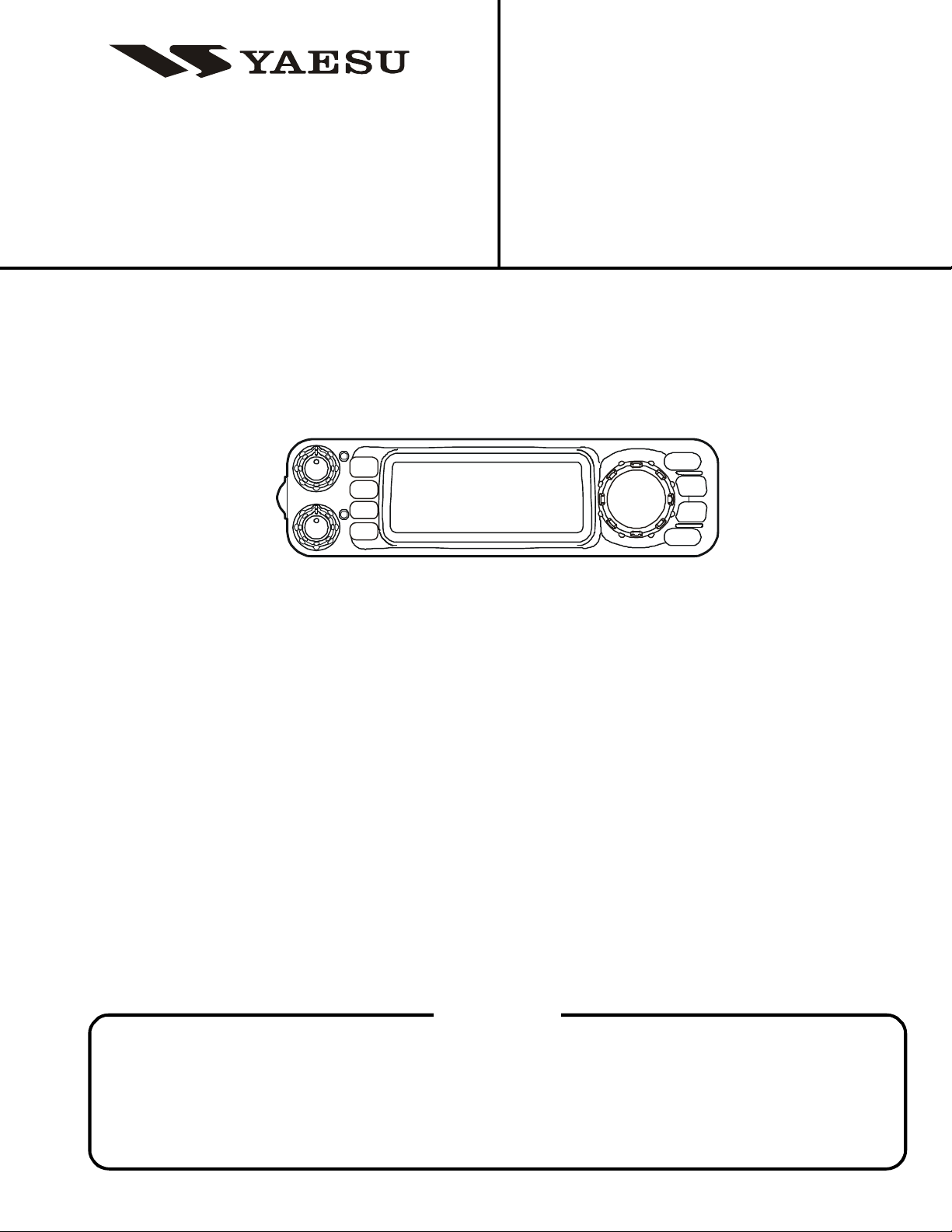
VHF/UHF Dual Band
POWER
TONE
FM Transceiver
FT-7100M
Technical Supplement
©2002 VERTEX STANDARD CO., LTD. Printed in Japan.
EH003M90A
BAND
V/M
HOME
MHz
VERTEX STANDARD CO., LTD.
4-8-8 Nakameguro, Meguro-Ku, Tokyo 153-8644, Japan
VERTEX STANDARD
US Headquarters
10900 Walker Street, Cypress, CA 90630, U.S.A.
International Division
8350 N.W. 52nd Terrace, Suite 201, Miami, FL 33166, U.S.A.
YAESU EUROPE B.V.
P.O. Box 75525, 1118 ZN Schiphol, The Netherlands
YAESU UK LTD.
Unit 12, Sun Valley Business Park, Winnall Close
Winchester, Hampshire, SO23 0LB, U.K.
VERTEX STANDARD HK LTD.
Unit 5, 20/F., Seaview Centre, 139-141 Hoi Bun Road,
Kwun Tong, Kowloon, Hong Kong
LOW
REV
Introduction
This manual provides technical information necessary for servicing the FT-7100M FM Transceiver.
Servicing this equipment requires expertise in handling surface-mount chip components. Attempts by non-qualified
persons to service this equipment may result in permanent damage not covered by the warranty, and may be illegal in
some countries.
Two PCB layout diagrams are provided for each double-sided circuit board in the repeater. Each side of is referred to
by the type of the majority of components installed on that side (“leaded” or “chip-only”). In most cases one side has only
chip components, and the other has either a mixture of both chip and leaded components (trimmers, coils, electrolytic
capacitors, ICs, etc.), or leaded components only.
While we believe the technical information in this manual to be correct, VERTEX STANDARD assumes no liability
for damage that may occur as a result of typographical or other errors that may be present. Your cooperation in pointing
out any inconsistencies in the technical information would be appreciated.
Contents
Specifications................................................. 2
Exploded View & Miscellaneous Parts......3
Block Diagram...............................................4
Circuit Description .................................. 5
Alignment.................................................. 9
Board Unit (
Schematics, Layouts & Parts
MAIN Unit .............................................................17
PANEL Unit ...........................................................53
VR Unit ..................................................................65
)
1

Specifications
GENERAL
Frequency Range: RX: 108.00 – 180.00 MHz
320 – 480 MHz
810 – 999.990 MHz (Cellular Blocked)
TX: 144 – 146 MHz or 144 – 148 MHz
430 – 440 MHz or 430 – 450 MHz
Channel Steps: 5/10/12.5/15/20/25/50 kHz
Mode of Emission: F3, F2, F1
Antenna Impedance: 50 Ω, unbalanced (Antenna Duplexer built-in)
Frequency Stability: ±5 ppm @ 14°F ~ +140°F (–10°C ~ +60°C)
Operating Temperature Range: –4°F ~ +140°F (–20°C ~ +60°C)
Supply Voltage: 13.8 VDC (±15%), negative ground
Current Consumption (Approx.):RX: 0.5 A (Squelched)
TX: 11.5 A (VHF), 10.0 A (UHF)
Case Size (WxHxD): 5.8 x 1.9 x 6.9 inches (140 x 38 x 166 mm)
(w/o knobs & connectors)
Weight (Approx.): 2.2 lb (1 kg)
TRANSMITTER
Output Power: 50/20/10/5 W (VHF), 35/20/10/5 W (UHF)
Modulation Type: Variable Reactance
Maximum Deviation: ±5 kHz
Spurious Radiation: Better than –60 dB
Modulation Distortion: Less than 3%
Microphone Impedance: 2 kΩ
DATA Jack Impedance: 10 kΩ
RECEIVER
Circuit Type: Double-conversion superheterodyne
Intermediate Frequencies: 21.7 MHz/450 kHz (VHF), 45.05 MHz/455 kHz (UHF)
Sensitivity (for 12dB SINAD): Better than 0.16 µV
Squelch Sensitivity: 0.1 µV
Image Rejection: 70 dB
Selectivity (–6dB/–60dB): 12 kHz/24 kHz
Maximum AF Output: 2 W @ 8 Ω for 10% THD
AF Output Impedance: 4 – 16 Ω
Specifications are subject to change without notice, and are guaranteed within the 144 and 430 MHz amateur bands only.
Frequency ranges will vary according to transceiver version; check witj your dealer.
2
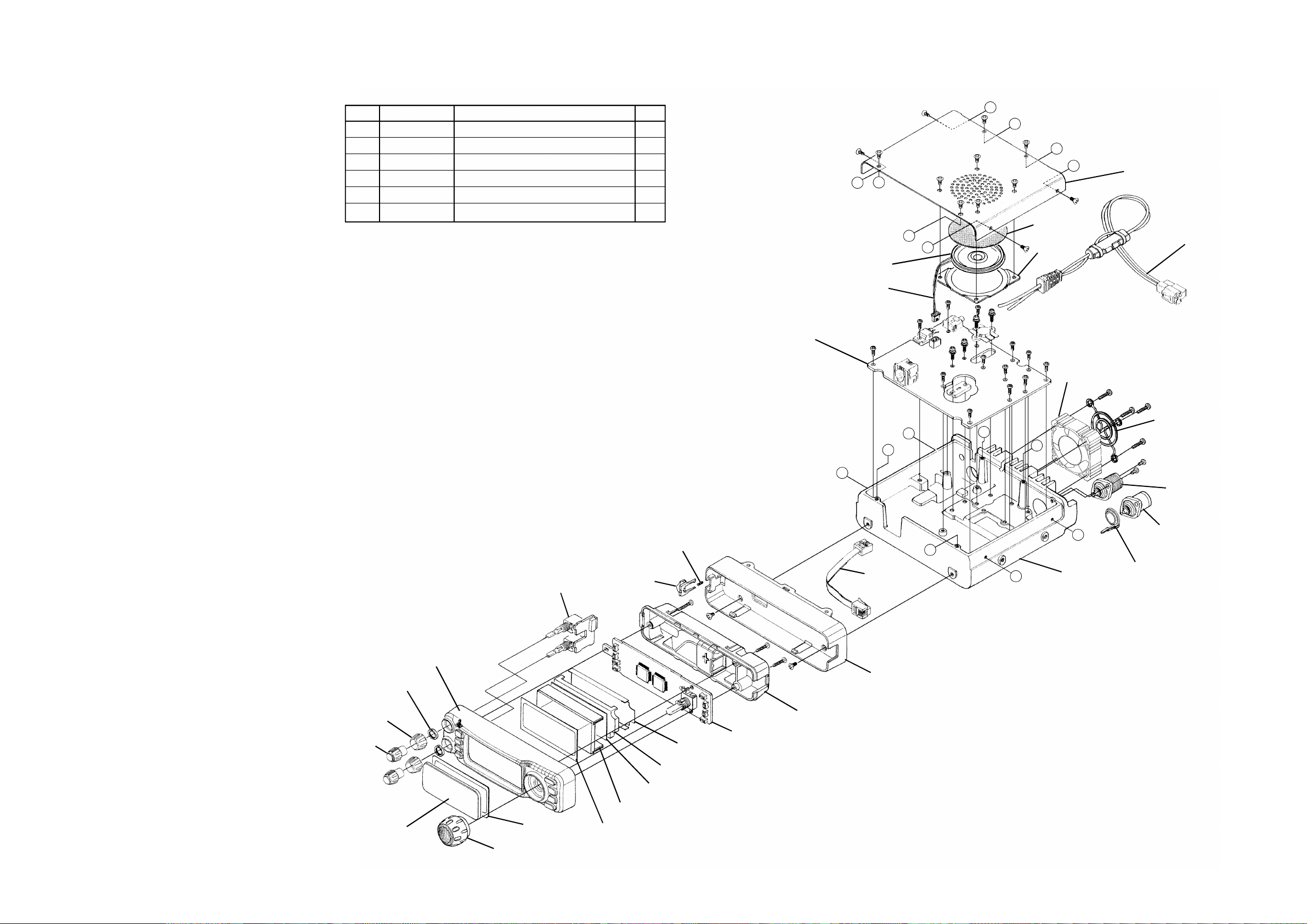
Exploded View & Miscellaneous Parts
REF. VXSTD P/N Description Qty.
1 U31206007 OVAL HEAD SCREW M2.6x6B 14
2 U44308002 TAPTITE SCREW M3x8NI 13
3 U03310002 SEMS SCREW ASM3x10NI 4
4 U43212007 TAPTITE SCREW M2.6x12B 3
5 U20308002 BINDING HEAD SCREW M3x8NI 2
6 U20318007 BINDING HEAD SCREW M3x18B 4
MAIN Unit
À
H
M4090149
SPEAKER
T9206082
CW ASSY
H
Á
À
À
A
À
B
À
À
À
G
À
F
E
À
À
C
RA02132A0
NYLON MESH
R0150630
À
HOLDER
D
CS1739001
CASE ASSY
À
T9206761
WIRE ASSY
Á
Á
Â
Â
Â
Á
Á
Â
Á
Á
Á
C
Á
M2090034
FAN
Å
Å
Å
Å
S5000206
FAN GUARD
Á
Á
Á
B
Ä
Ä
P1090984
CONNECTOR (USA, AUS)
Á
A
G
RA027330A
SPECIAL NUT (x2 pcs)
RA027330A
KNOB (SQL) (x2 pcs)
RA027340A
KNOB (AF) (x2 pcs)
RA0292900
FRONT PANEL ASSY
RA0268900
WINDOW
VR Unit
RA0274100
DOUBLE FACE
RA027320A
ENCODER KNOB
R0137551
COIL SPRING
RA026900A
RELEASE KNOB
RA0276000
RUBBER CONNECTOR (x2 pcs)
RA0274000
SHEET
Ã
À
RA0273900
REFLECTOR SHEET
RA0268700
LIGHT GUIDE
RA0273800
DIFFUSER SHEET
Ã
Ã
PANEL Unit
À
RA026850A
REAR PANEL
T9101509
CT CABLE
RA026860A
SUB PANEL
D
P1090547
CONNECTOR (EXP)
F
E
RA026680A
CHASSIS
S5000236
LUG WASHER (EXP)
3
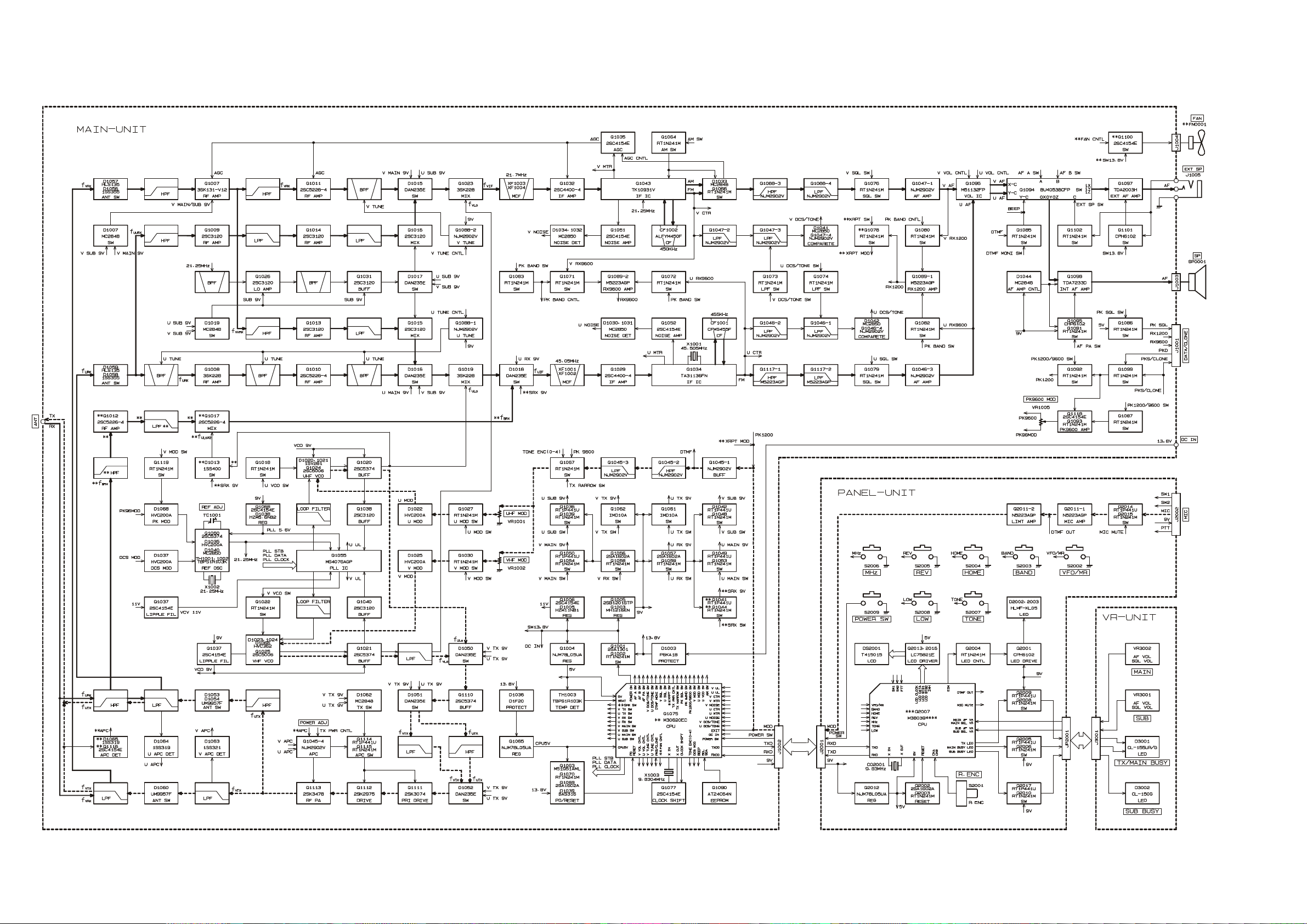
Block Diagram
4

Circuit Description
VHF Reception
Incoming VHF signals are passed through a low-pass
filter network, antenna switching diodes D1056 (1SS355)
and D1057 (RLS135), and a high-pass filter network, and
on to the RF amplifier Q1007 (3SK131). The amplified
RF signal is passed through another RF amplifier Q1011
(2SC5226) and band-pass filtered again by varactor-tuned
resonators L1022, L1029, L1034 and D1009, D1012, D1014
(all HVU359), then applied to the 1st mixer Q1023
(3SK228) along with the first local signal from the PLL
circuit.
The first local signal is generated between 122.3 MHz
and 126.3 MHz by the VHF VCO, which consists of Q1025
(2SC5006) and varactor diodes D1023, D1024, and D1066
(all HSV362) according to the receiving frequency.
The 21.7 MHz first IF signal is applied to monolithic
crystal filters XF1003 and XF1004 (both 21R12B5) which
strip away unwanted mixer products, and the IF signal is
applied to the first IF amplifier Q1032 (2SC4400). The
amplified first IF signal is then delivered to the FM IF subsystem IC Q1043 (TK10931V), which contains the second
mixer, limiter amplifier, noise amplifier, and FM detector.
The second local signal is generated by 21.25 MHz crystal X1002 and Q1060 (2SC5374), producing the 450 kHz
second IF signal when mixed with the first IF signal within Q1043.
The 450 kHz second IF signal is applied to the ceramic
filter CF1002 (ALFYM450F) which strips away all but the
desired signal, and then passes through the limiter amplifier within Q1043 to the ceramic discriminator CD1002
(CDBM450C7), which removes any amplitude variations
in the 450 kHz IF signal before detection of speech.
The detected audio passes through the de-emphasis
network, a high-pass filter consisting of Q1088
(NJM2902V-3) and associated circuitry, and a low-pass
filter consisting of Q1088 (NJM2902V-4) and associated
circuitry. The filtered audio signal is amplified by Q1047
(NJM2902V-1), then passes through the audio volume
control IC Q1096 (M511312FP) which adjusts the audio
sensitivity to compensate for audio level variations, and
then is delivered to audio switch Q1094 (BU4053BCFV).
When the internal speaker is selected, the audio signal
is amplified by Q1098 (TDA7233D), then applied to the
internal loudspeaker. When the external speaker is selected, the audio signal is amplified by Q1097 (TDA2003H),
then it passes through the EXT SP jack to the external loudspeaker.
UHF Reception
Incoming UHF signals are passed through a low-pass
filter network, high-pass filter network, antenna switching diodes D1058 (1SS355) and D1059 (RLS135), and
on to the band-pass filter network consisting of varactor
diode D1004 (HVU359) and L1001.
The filtered UHF signal is amplified by RF amplifier
Q1008 (3SK228) and fed to another band-pass filter consisting of varactor diode D1006 (HVU359) and L1008, and
then is passed through another RF amplifier Q1010
(2SC5226) to another band-pass filter consisting of varactor diodes D1010 and D1011 (both HVU359) and L1027/
L1030.
The amplified and filtered UHF signal is applied to
the 1st mixer Q1019 (3SK228) along with the first local
signal from the PLL circuit.
The first local signal is generated between 384.95 MHz
and 404.95 MHz by the UHF VCO, which consists of
Q1024 (2SC5006) and varactor diodes D1020 (1SV281)
and D1021 (1SV280), according to the receiving frequency.
The 45.05 MHz first IF signal is applied to monolithic
crystal filters XF1001 and XF1002 (both 45M15B5H)
which strip away unwanted mixer products, and the IF
signal is applied to the first IF amplifier Q1029 (2SC4400).
The amplified first IF signal is then delivered to the FM IF
subsystem IC Q1034 (TA31136FN), which contains the
second mixer, limiter amplifier, noise amplifier, and FM
detector.
The second local signal is generated by 45.505 MHz
crystal X1001, producing the 455 kHz second IF signal
when mixed with the first IF signal within Q1034.
The 455 kHz second IF signal is applied to the ceramic
filter CF1001 (CFW455F) which strips away all but the
desired signal, and then passes through the limiter amplifier within Q1034 to the ceramic discriminator CD1001
(CDBM455C7), which removes any amplitude variations
in the 455 kHz IF signal before detection of speech.
5

Circuit Description
The detected audio passes through the de-emphasis
network, a high-pass filter consisting of Q1117
(M5223AGP-1) and associated circuitry, and a low-pass
filter consisting of Q1117 (M5223AGP-2) and associated
circuitry. The filtered audio signal is amplified by Q1046
(NJM2902V-3), then passes through the audio volume
control IC Q1096 (M511312FP), which adjusts the audio
sensitivity to compensate for audio level variations, and
then is delivered to audio switch Q1094 (BU4053BCFV).
When the internal speaker is selected, the audio signal
is amplified by Q1098 (TDA7233D) then applied to the
internal loudspeaker. When the external speaker is selected, the audio signal is amplified by Q1097 (TDA2003H),
then it passes through the EXT SP jack to the external
loudspeaker.
V/V (VHF-VHF) Dual Reception
During V&V operation, the incoming VHF "sub" band
signal is passed through a low-pass filter network, antenna switching diode D1056 (1SS355), D1057 (RLS135) and
a high-pass filter network to the RF amplifier Q1007
(3SK131). The amplified RF signal is passed through a
high-pass filter network, VHF "sub" RF amplifier Q1013
(2SC3120), and a low-pass filter network, then is applied
to the VHF "sub" first mixer Q1015 (2SC3120) along with
the 255 MHz VHF "sub" first local signal from the PLL
circuit.
The 399 ~ 403 MHz VHF "sub" first IF signal is applied
to the VHF "sub" second IF mixer Q1019 (3SK228) along
with the VHF "sub" second local signal from the PLL circuit. The VHF "sub" second local signal is generated between 444.05 MHz and 448.05 MHz by the UHF VCO
Q1023.
The 45.05 MHz VHF "sub" second IF signal is applied
to the UHF receiving circuit. The VHF "sub" signal is amplified, filtered, and demodulated, etc., by the UHF "main"
receiving circuit, described previously.
U/U (UHF-UHF) Dual Reception
During U/U operation, the incoming UHF "sub" band
signal is passed through high-pass and low-pass filter
networks, antenna switching diodes D1058 (1SS355) and
D1059 (RLS135), and another high-pass filter network to
the RF amplifier Q1009 (2SC3120). The amplified RF signal is passed through a low-pass filter network, UHF "sub"
RF amplifier Q1014 (2SC3120), and low-pass filter network, then is applied to the UHF "sub" first mixer Q1016
(2SC3120) along with the 255 MHz UHF "sub" first local
signal from the PLL circuit.
The 175 ~ 195 MHz UHF "sub" first IF signal is applied
to the UHF "sub" second IF mixer Q1023 (3SK228) along
with the UHF "sub" second local signal from the PLL circuit. The UHF "sub" second local signal is generated between 153.30 MHz and 173.30 MHz by the VHF VCO
Q1025.
The 21.7 MHz UHF "sub" second IF signal applied to
VHF receiving circuit. The UHF "sub" signal is amplified,
filtered, and demodulated, etc., by the VHF receiving circuit, described previously.
VHF Squelch Control
When no VHF carrier is being received, noise at the
output of the detector stage in Q1043 is amplified and
band-pass filtered by the noise amp section of Q1043, then
passes through the noise amplifier Q1051 (2SC4154E) to
noise detector D1034 (MC2850). The resulting DC voltage is applied to pin 93 of main CPU Q1075
(M30620ECGP), which compares the squelch threshold
level to that which set by the front panel VHF SQL knob.
While no carrier is received, pin 76 of Q1075 remains
"high," turning on the squelch switch Q1076 (RT1N241M)
to disable audio output from the speaker.
UHF Squelch Control
When no UHF carrier is being received, noise at the
output of the detector stage in Q1034 is amplified and
band-pass filtered by the noise amp section of Q1034, then
passes through the noise amplifier Q1052 (2SC4154E) to
noise detector D1030 (MC2850). The resulting DC voltage is applied to pin 89 of main CPU Q1075, which compares the squelch threshold level to that which set by the
front panel UHF SQL knob.
6

Circuit Description
While no carrier is received, pin 75 of Q1075 remains
"high," turning on the squelch switch Q1079 (RT1N241M)
to disable audio output from the speaker.
Transmit Signal Path
The speech signal from the microphone passes through
the MIC jack J2002 to AF amplifier Q2011 (M5223AGP)
on the PANEL UNT. The amplified speech signal is subjected to amplitude limiting by Q2011 (M5223AGP), then
passes through the panel interface jacks J2001 and J1002
to MAIN Unit. On the MAIN UNIT, the speech signal
passes through buffer amplifier Q1045 (NJM2902V-1/-2)
and a low-pass filter network at Q1045 (NJM2902V-3) to
deviation control VR1001 (for UHF Tx audio) or VR1002
(for VHF Tx audio).
VHF Transmit Signal Path
The adjusted speech signal from VR1002 is delivered
to VHF VCO Q1025, which frequency modulates the
transmitting VCO D1025 (HVC200A).
The 35-Watt RF signal passes through a high-pass fil-
ter network, antenna switch D1053 and D1054
(UM9957F), low-pass filter and high-pass filter networks,
and then is delivered to the ANT jack.
VHF Tx APC Circuit
A portion of the power amplifier output is rectified by
D1063 (1SS321), D1065 (1SS319) and Q1116
(2SC4154E), then delivered to APC Q1045 (NJM2902V)
as a DC voltage which is proportional to the output level
of the power amplifier.
The APC Q1045 compares the rectified DC voltage
from the power amplifier and the reference voltage from
the main CPU Q1075, producing a control voltage for the
Automatic Power Controller Q1114 (RT1P441U) and
Q1115 (RT1N241M) which regulates supply voltage to
the Pre-Drive amplifier Q1111, Drive amplifier Q1112,
and Power amplifier Q1113, so as to maintain stable output power under varying antenna loading conditions.
The modulated transmit signal passes through buffer
amplifier Q1021 (2SC5374), a low-pass filter network, and
another buffer amplifier Q1110 (2SC5374) to another lowpass filter network.
The filtered transmit signal is applied to the Pre-Drive
amplifier Q1111 (2SK3074) and Drive amplifier Q1112
(2SK2975), then finally is amplified by Power amplifier
Q1113 (2SK3478) up to 50 Watts. This three stage power
amplifier’s gain is controlled by the APC circuit.
The 50-Watt RF signal passes through a low-pass filter
network, antenna switch D1060 (UM9957F), and another
low-pass filter network, and then is delivered to the ANT
jack.
UHF Transmit Signal Path
The adjusted speech signal from VR1001 is delivered
to UHF VCO Q1024 which frequency modulates the transmitting VCO D1022 (HVC200A).
The modulated transmit signal passes through buffer
amplifiers Q1020 and Q1110 (both 2SC5374) to a highpass filter network.
The filtered transmit signal is applied to the Pre-Drive
amplifier Q1111 (2SK3074) and Drive amplifier Q1112
(2SK2975), then finally is amplified by Power amplifier
Q1113 (2SK3478) up to 35 Watts. This three stage power
amplifier’s gain is controlled by the APC circuit.
UHF Tx APC Circuit
A portion of the power amplifier output is rectified by
D1064 (1SS319), D1065 (1SS319) and Q1116
(2SC4154E), then delivered to APC Q1045 (NJM2902V)
as a DC voltage which is proportional to the output level
of the power amplifier.
The APC Q1045 compares the rectified DC voltage
from the power amplifier and the reference voltage from
the main CPU Q1075, producing a control voltage for the
Automatic Power Controller Q1114 (RT1P441U) and
Q1115 (RT1N241M) which regulates supply voltage to
the Pre-Drive amplifier Q1111, Drive amplifier Q1112,
and Power amplifier Q1113, so as to maintain stable output power under varying antenna loading conditions.
VHF PTT Circuit
When the PTT switch is pressed, pin 46 of sub CPU
Q2007 (M38039FFFP) goes “1V,” which sends the “PTT”
command to the main CPU, Q1075. When it receives the
“PTT” command, pin85 of Q1075 goes “high” to control
local switch D1050 (DAN235E), filter switch D1051,
D1052, TX switch D1062 (MC2848), and APC switch
Q1114/Q1115, which activates the VHF Tx circuit. Mean-
while, pin 86 of Q1075 goes “low,” which disables the
VHF Rx circuit.
7

Circuit Description
UHF PTT Circuit
When the PTT switch is pressed, pin 46 of sub CPU
Q2007 (M38039FFFP) goes “1V,” which sends the “PTT”
command to the main CPU, Q1075. When it receives the
“PTT” command, pin81 of Q1075 goes “high” to controls
local switch D1050, filter switch D1051, D1052, TX switch
D1062 and APC switch Q1114/Q1115, which activates the
UHF Tx circuit. Meanwhile, pin 82 of Q1075 goes “low,”
which disables the UHF Rx circuit.
VHF PLL
A portion of the output from the VHF VCO Q1025
(2SC5006) passes through buffer amplifiers Q1021
(2SC5374) and Q1040 (2SC3120) to the programmable
divider section of the PLL IC Q1055 (M64076AGP), which
divides the frequency according to the frequency dividing data from the main CPU, Q1075. It is then sent to the
phase comparator.
The 21.25 MHz frequency of the reference oscillator
circuit, made up of X1002 and Q1060 (2SC5374), is divided by the reference frequency divider section of Q1055
into 4250 or 3400 parts to become 5 kHz or 6.25 kHz comparative reference frequencies, which are utilized by the
phase comparator.
The phase comparator section of Q1055 compares the
phase between the frequency-divided oscillation frequency of the VCO circuit and comparative frequency, and its
output is a pulse corresponding to the phase difference.
This pulse is integrated by the charge pump and loop filter of Q1055 into a control voltage (VCV) to control the
oscillation frequency of the VHF VCO Q1025.
UHF PLL
A portion of the output from the UHF VCO Q1024
(2SC5006) passes through buffer amplifier Q1020
(2SC5374) and Q1038 (2SC3120) to the programmable
divider section of the PLL IC Q1055 (M64076AGP), which
divides the frequency according to the frequency dividing data from the main CPU Q1075. It is then sent to the
phase comparator.
The 21.25 MHz frequency of the reference oscillator
circuit, made up of X1002 and Q1060 (2SC5374), is divided by the reference frequency divider section of Q1055
into 4250 or 3400 parts to become 5 kHz or 6.25 kHz comparative reference frequencies, which are utilized by the
phase comparator.
The phase comparator section of Q1055 compares the
phase between the frequency-divided oscillation frequency of the VCO circuit and comparative frequency, and its
output is a pulse corresponding to the phase difference.
This pulse is integrated by the charge pump and loop filter of Q1055 into a control voltage (VCV) to control the
oscillation frequency of the UHF VCO Q1024.
V/V, U/U Local Oscillator
When the V/V or U/U feature is activated, a portion of
the 21.25 MHz reference is amplified and multiplied by
twelve by Q1026 (2SC3120), then passes through bandpass filter network to buffer amplifier Q1031 (2SC3120),
which provides the first local signal for V/V or U/U operation.
Power-on Circuit
When the POWER switch is turned on, pin 16 of main
CPU Q1075 goes “low.” When pin 16 of Q1075 goes
“low,” pin 61 of Q1075 goes “high” to activate the power
switches Q1001 (2SA1301) and Q1002 (RT1N241M),
which supply the DC power to the radio.
8

Alignment
Introduction and Precautions
The FT-7100M has been carefully aligned at the factory for the specified performance across the 144 MHz and
430 MHz amateur bands. Realignment should therefore
not be necessary except in the event of a component failure. All component replacement and service should be
performed only by an authorized VERTEX STANDARD
representative, or the warranty policy may be voided.
The following procedures cover the sometimes critical and tedious adjustments that are not normally required
once the transceiver has left the factory. However, if damage occurs and some parts are replaced, realignment may
be required. If a sudden problem occurs during normal
operation, it is likely due to component failure; realignment should not be done until after the faulty component
has been replaced.
We recommend that servicing be performed only by
authorized VERTEX STANDARD service technicians, who
are experienced with the circuitry and fully equipped for
repair and alignment. Therefore, if a fault is suspected,
contact the dealer from whom the transceiver was purchased for instructions regarding repair. Authorized VERTEX STANDARD service technicians realign all circuits
and make complete performance checks to ensure compliance with factory specifications after replacing any
faulty components.
Those who do undertake any of the following alignments are cautioned to proceed at their own risk. Problems caused by unauthorized attempts at realignment are
not covered by the warranty policy. Also, VERTEX STANDARD must reserve the right to change circuits and alignment procedures in the interest of improved performance,
without notifying owners.
Under no circumstances should any alignment be attempted unless the normal function and operation of the
transceiver are clearly understood, the cause of the malfunction has been clearly pinpointed and any faulty components replaced, and the need for realignment determined to be absolutely necessary.
Required Test Equipment
The following test equipment (and thorough familiarity with its correct use) is necessary for complete realignment. Correction of problems caused by misalignment
resulting from use of improper test equipment is not covered under the warranty policy. While most steps do not
require all of the equipment listed, the interactions of some
adjustments may require that more complex adjustments
be performed afterwards. Do not attempt to perform only
a single step unless it is clearly isolated electrically from
all other steps. Have all test equipment ready before beginning, and follow all of the steps in a section in the order presented.
r Regulated DC Power Supply: adjustable from 10 to 17
VDC, 15 A
r RF Signal Generator with calibrated output level at 500
MHz
r Frequency Counter: ±0.1 ppm accuracy at 500 MHz
r AF Signal Generator
r SINAD Meter
r Oscilloscope
r Spectrum Analyzer
r Deviation Meter (linear detector)
r AF Milivoltmetr
r AF Dummy Load: 4 Ohms, 5 W
r DC Voltmeter: high impedance
r Inline Wattmeter with 5% accuracy at 500 MHz
r 50-Ohm non-reactive Dummy Load: 100 watts at 500
MHz
r VHF/UHF Sampling Coupler
9
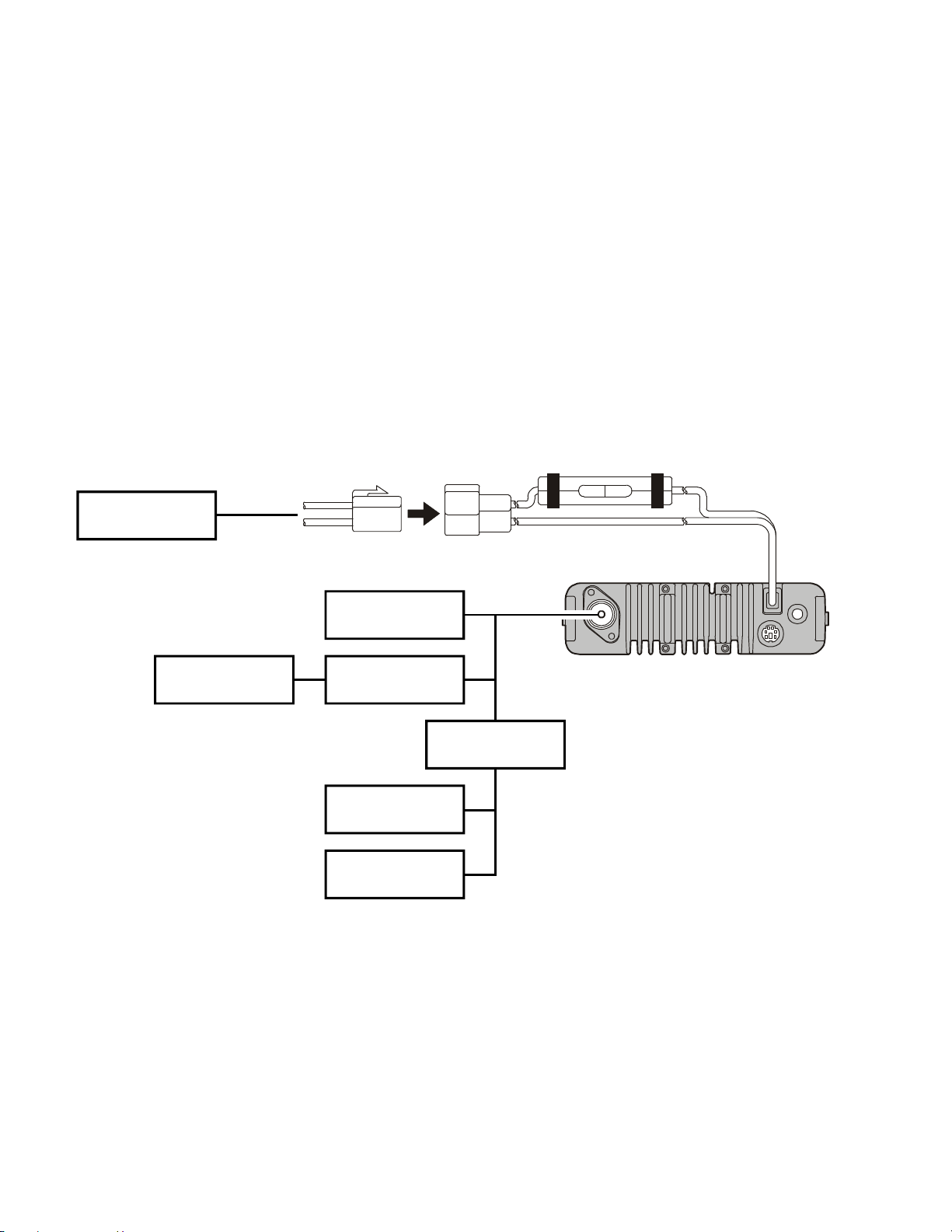
DATA
EXT SP
13.8VDC
Alignment
Alignment Preparation & Precautions
A dummy load and inline wattmeter must be connected to the main antenna jack in all procedures that call for
transmission, except where specified otherwise. Correct
alignment is not possible with an antenna. After completing one step, read the following step to determine whether the same test equipment will be required. If not, remove the test equipment (except dummy load and wattmeter, if connected) before proceeding.
Correct alignment requires that the ambient temperature in the repair shop be the same as that of the trans-
Power Supply
10 ~17 V DC, 15A
ceiver and test equipment, and that this temperature be
held constant between 68 °F and 86 °F (20 °C ~ 30 °C).
When the transceiver is brought into the shop from hot or
cold air it should be allowed some time for thermal equalization with the environment before alignment. If possible, alignments should be made with oscillator shields and
circuit boards firmly affixed in place. Also, the test equipment must be thoroughly warmed up before beginning.
Note: Signal levels in dB referred to in alignment are based on
0 dBµ = 0.5 µV. (closed circuit).
Dummy Load
ANT
RF Signal
Generator
Inline Wattmeter
ATT
Deviation
Meter
Frequency
Counter
10
Alignment
PLL Reference Frequency
r Connect the wattmeter, dummy load, and fre-
quency counter to the antenna jack.
r Tune the transceiver to 439.900 MHz, and set the
TX power level to “MID 2.”
r Key the transceiver, and adjust TC1001 on the
MAIN UNIT, if necessary, so the counter frequency is within 100 Hz of 439.900 MHz.
VHF Transmitter Deviation
r Connect the wattmeter, dummy load, and devia-
tion meter to the antenna jack.
r Inject a 1 kHz audio signal at a level of 50 mV to
pin 5 of the MIC jack (pin 4 is Ground).
r Key the transmitter on 146.000 MHz. Adjust
VR1002 for 4.0 ±0.5 kHz (for USA version; other
versions: 4.5 ± 0.5 kHz) deviation on the deviation meter.
UHF Transmitter Deviation
r Leave the wattmeter, dummy load, and deviation
meter connected to the antenna jack.
r Inject a 1 kHz audio signal as a level of 50 mV to
pin 5 of the MIC jack (pin 4 is Ground).
r Key the transmitter on 440.000 MHz. Adjust
VR1001 for 4.0 ±0.5 kHz (for USA version; other
versions: 4.5 ± 0.5 kHz) deviation on the deviation meter.
VR1001 TC1001VR1002
11
Alignment
Internal System Alignment Routine
This uses a programmed routine in the transceiver
which simplifies many complex discrete component settings and adjustments using digitally-controlled settings
via the front panel’s buttons and LCD indications.
The examples below assume that the transceiver is to
be used in a 4-MHz-wide band (144-148 MHz). The factory-default settings for the FT-7100M assume a wider transmit frequency range, so a "trick" must be used to set up
the frequencies correctly.
m In the Alignment mode, a special memory table
(see below) is temporarily established, providing
pre-set frequencies to be used in the alignment
process.
CH VHF UHF
1 108.000 MHz 360.000 MHz
2 137.000 MHz 390.000 MHz
3 144.000 MHz 430.000 MHz
4 146.000 MHz 440.000 MHz
5 148.000 MHz 450.000 MHz
6 165.000 MHz 460.000 MHz
7 180.000 MHz 480.000 MHz
Note: For transceivers operating on 144-146 MHz,
use more appropriate frequencies, like
145.000/435.000 MHz (CH 4), 146.000/
440.000 MHz (CH 5).
m To enter the Alignment mode, turn the transceiver
off.
Now, short pins 1 and 6 of the MIC jack to Ground
(pin 4). While these two pins are shorted to
ground, press and hold in the HOME key while
turning the transceiver on.
m Disconnect the shorting of pins 1 and 6 of the MIC
jack to Ground; the transceiver is now in the
Alignment mode.
m In the Alignment mode, each Alignment Menu is
selected by the LOW (increase) and REV (de-
crease) keys; band change (VHF or UHF) is ac-
complished by the BAND key; and adjustment of
the setting is accomplished by rotating the Dial
knob.
m Once you have completed adjustment of each re-
quired Alignment Menu item, pressing the TONE
key will lock in that setting.
m If the alignment step requires that you “key the
transmitter,” this may be accomplished by short-
ing pin 6 of the MIC jack to Ground.
m To save all settings and exit to normal operation,
press the V/M key.
UHF Transmitter Output
r Connect the wattmeter and dummy load to the
antenna jack.
r Enter the Alignment mode, then press the LOW
and/or REV keys on the panel to select “POMAX.”
r Press the BAND key to select “U4 xxx ,” if neces-
sary (xxx = parameter).
r Key the transmitter, and confirm that the output
power is more than 38 Watts.
r Press the LOW and/or REV keys on the panel to
select “PO HI.” Press the BAND key to select “U3
xxx,” if necessary (xxx = parameter).
r Key the transmitter, and rotate the Dial knob so
as to achieve 35 watts (±0.5 W) on the wattmeter.
r Press the LOW key to select “U4 xxx,” if neces-
sary (xxx = parameter).
r Key the transmitter, and rotate the Dial knob so
as to achieve 35 watts (±0.5 W) on the wattmeter.
r Press the LOW key to select “U5 xxx,” if neces-
sary (xxx = parameter).
r Key the transmitter, and rotate the Dial knob so
as to achieve 35 watts (±0.5 W) on the wattmeter.
r Press the LOW and/or REV keys on the panel to
select “PO M1.” Press the BAND key to select “U3
xxx,” if necessary (xxx = parameter).
r Key the transmitter, and rotate the Dial knob so
as to achieve 20 watts (±0.5 W) on the wattmeter.
r Press the LOW key to select “U4 xxx,” if neces-
sary (xxx = parameter).
r Key the transmitter, and rotate the Dial knob so
as to achieve 20 watts (±0.5 W) on the wattmeter.
r Press the LOW key to select “U5 xxx,” if neces-
sary (xxx = parameter).
r Key the transmitter, and rotate the Dial knob so
as to achieve 20 watts (±0.5 W) on the wattmeter.
r Press the LOW and/or REV keys on the panel to
select “PO M2.” Press the BAND key to select “U3
xxx,” if necessary (xxx = parameter).
r Key the transmitter, and rotate the Dial knob so
as to achieve 10 watts (±0.5 W) on the wattmeter.
r Press the LOW key to select “U4 xxx,” if neces-
sary (xxx = parameter).
r Key the transmitter, and rotate the Dial knob so
as to achieve 10 watts (±0.5 W) on the wattmeter.
r Press the LOW key to select “U5 xxx,” if neces-
sary (xxx = parameter).
r Key the transmitter, and rotate the Dial knob so
as to achieve 10 watts (±0.5 W) on the wattmeter.
r Press the LOW and/or REV keys on the panel to
select “PO LO.” Press the BAND key to select “U3
xxx,” if necessary (xxx = parameter).
12

Alignment
r Key the transmitter, and rotate the Dial knob so
as to achieve 5 watt (±0.5 W) on the wattmeter.
r Press the LOW key to select “U4 xxx,” if neces-
sary (xxx = parameter).
r Key the transmitter, and rotate the Dial knob so
as to achieve 5 watt (±0.5 W) on the wattmeter.
r Press the LOW key to select “U5 xxx,” if neces-
sary (xxx = parameter).
r Key the transmitter, and rotate the Dial knob so
as to achieve 5 watt (±0.5 W) on the wattmeter.
r Press the V/M key to save the new settings and
exit.
UHF DCS Deviation
r Connect the wattmeter, dummy load and devia-
tion meter to the antenna jack.
r Enter the Alignment mode, then press the LOW
and/or REV keys on the panel to select “DCS M.”
r Press the BAND key to select “U4 xxx,” if neces-
sary (xxx = parameter).
r Key the transmitter, and rotate the Dial knob so
as to achieve 0.6 kHz (±0.2 kHz) on the deviation
meter.
r Press the V/M key to save the new setting and
exit.
UHF Receiver
r Connect the RF signal generator to the antenna
jack, and inject an RF signal from the signal generator at 10 dBµ on the "Memory Channel 1" frequency with ±3.5 kHz deviation of a 1 kHz tone.
r Enter the Alignment mode, then press the LOW
and/or REV keys on the panel to select “TUNE 1.”
r Rotate the Dial knob so as to obtain the maximum
numerical value in the memory channel area on
the transceiver’s display.
r Inject an RF signal from the signal generator at
10 dBµ on the "Memory Channel 2" frequency
with ±3.5 kHz deviation of a 1 kHz tone.
r Press the LOW and/or REV keys on the panel to
select “TUNE 2.”
r Rotate the Dial knob so as to obtain the maximum
numerical value in the memory channel area on
the transceiver’s display.
r Inject an RF signal from the signal generator at
10 dBµ on the "Memory Channel 3" frequency
with ±3.5 kHz deviation of a 1 kHz tone.
r Press the LOW and/or REV keys on the panel to
select “TUNE 3.”
r Rotate the Dial knob so as to obtain the maximum
numerical value in the memory channel area on
the transceiver’s display.
r Inject an RF signal from the signal generator at
10 dBµ on the "Memory Channel 4" frequency
with ±3.5 kHz deviation of a 1 kHz tone.
r Press the LOW and/or REV keys on the panel to
select “TUNE 4.”
r Rotate the Dial knob so as to obtain the maximum
numerical value in the memory channel area on
the transceiver’s display.
r Inject an RF signal from the signal generator at
10 dBµ on the "Memory Channel 5" frequency
with ±3.5 kHz deviation of a 1 kHz tone.
r Press the LOW and/or REV keys on the panel to
select “TUNE 5.”
r Rotate the Dial knob so as to obtain the maximum
indication in the memory channel area on the
transceiver’s display.
r Inject an RF signal from the signal generator at
10 dBµ on the "Memory Channel 6" frequency
with ±3.5 kHz deviation of a 1 kHz tone.
r Press the LOW and/or REV keys on the panel to
select “TUNE 6.”
r Rotate the Dial knob so as to obtain the maximum
numerical value inthe memory channel area on
the transceiver’s display.
r Inject an RF signal from the signal generator at
10 dBµ on the "Memory Channel 7" frequency
with ±3.5 kHz deviation of a 1 kHz tone.
r Press the LOW and/or REV keys on the panel to
select “TUNE 7.”
r Rotate the Dial knob so as to obtain the maximum
numerical value in the memory channel area on
the transceiver’s display.
r Press the V/M key to save the new settings and
exit.
UHF Discriminator Center Meter Calibration
r Connect the RF signal generator to the antenna
jack, and inject an RF signal from the signal generator at 20 dBµ on 439.9975 MHz (2.5 kHz below Memory Channel 4) with ±3.5 kHz deviation
of a 1 kHz tone.
r Enter the Alignment mode, then press the LOW
and REV keys on the panel to select “CTR –.”
r Press the BAND key to select “U4 xxx ,” if neces-
sary (xxx = parameter).
r Press the TONE key.
r Inject an RF signal from the signal generator at
20 dBµ on 440.0025 MHz (2.5 kHz above Memory
Channel 4) with ±3.5 kHz deviation of a 1kHz
tone.
r Press the LOW and/or REV keys on the panel to
select “CTR +.”
r Press the TONE key.
r Press the V/M key to save the new setting and exit.
13

Alignment
UHF Squelch Threshold Calibration
r Connect the RF signal generator to the antenna
jack, and inject an RF signal from the signal gen-
erator at –13 dBµ on the "Memory Channel 4" fre-
quency with ±3.5 kHz deviation of a 1 kHz tone.
r Enter the Alignment mode, then press the LOW
and/or REV keys on the panel to select “SQL S.”
r Press the BAND key to select “U4 xxx ,” if neces-
sary (xxx = parameter).
r Press the TONE key.
r Press the V/M key to save the new setting and
exit.
UHF Tight Squelch Calibration
r Connect the RF signal generator to the antenna
jack, and inject an RF signal from the signal gen-
erator at 5 dBµ on the "Memory Channel 4" fre-
quency with ±3.5 kHz deviation of a 1 kHz tone.
r Enter the Alignment mode, then press the LOW
and/or REV keys on the panel to select “SQL T.”
r Press the BAND key to select “U4 xxx ,” if neces-
sary (xxx = parameter).
r Press the TONE key.
r Press the V/M key to save the new setting and
exit.
UHF S-Meter (S-1 Level) Calibration
r Connect the RF signal generator to the antenna
jack, and inject an RF signal from the signal gen-
erator at –8 dBµ on "Memory Channel 4" fre-
quency with ±3.5 kHz deviation of a 1 kHz tone.
r Enter the Alignment mode, then press the LOW
and/or REV keys on the panel to select “SMT 1.”
r Press the BAND key to select “U4 xxx ,” if neces-
sary (xxx = parameter).
r Press the TONE key.
r Press the V/M key to save the new setting and
exit.
UHF S-Meter (Full Scale) Calibration
r Connect the RF signal generator to the antenna
jack, and inject an RF signal from the signal gen-
erator at 25 dBµ on "Memory Channel 4" fre-
quency with ±3.5 kHz deviation of a 1 kHz tone.
r Enter the Alignment mode, then press the LOW
and/or REV keys on the panel to select “SMT F.”
r Press the BAND key to select “U4 xxx ,” if neces-
sary (xxx = parameter).
r Press the TONE key.
r Press the V/M key to save the new setting and
exit.
VHF Transmitter Output
r Connect the wattmeter and dummy load to the
antenna jack.
r Enter the Alignment mode, then press the LOW
and/or REV keys on the panel to select “POMAX.”
r Key the transmitter, and confirm that the output
power is more than 53 Watts.
r Press the LOW and/or REV keys on the panel to
select “PO HI.” Press the BAND key to select “V3
xxx,” if necessary (xxx = parameter).
r Key the transmitter, and rotate the Dial knob so
as to achieve 50 watts (±0.5 W) on the wattmeter.
r Press the BAND key to select “V4 xxx,” if neces-
sary (xxx = parameter).
r Key the transmitter, and rotate the Dial knob so
as to achieve 50 watts (±0.5 W) on the wattmeter.
r Press the BAND key to select “V5 xxx,” if neces-
sary (xxx = parameter).
r Key the transmitter, and rotate the Dial knob so
as to achieve 50 watts (±0.5 W) on the wattmeter.
r Press the LOW and/or REV keys on the panel to
select “PO M1.” Press the BAND key to select “V3
xxx,” if necessary (xxx = parameter).
r Key the transmitter, and rotate the Dial knob so
as to achieve 20 watts (±0.5 W) on the wattmeter.
r Press the BAND key to select “V4 xxx,” if neces-
sary (xxx = parameter).
r Key the transmitter, and rotate the Dial knob so
as to achieve 20 watts (±0.5 W) on the wattmeter.
r Press the BAND key to select “V5 xxx,” if neces-
sary (xxx = parameter).
r Key the transmitter, and rotate the Dial knob so
as to achieve 20 watts (±0.5 W) on the wattmeter.
r Press the LOW and/or REV keys on the panel to
select “PO M2.” Press the BAND key to select “V3
xxx,” if necessary (xxx = parameter).
r Key the transmitter, and rotate the Dial knob so
as to achieve 10 watts (±0.5 W) on the wattmeter.
r Press the BAND key to select “V4 xxx,” if neces-
sary (xxx = parameter).
r Key the transmitter, and rotate the Dial knob so
as to achieve 10 watts (±0.5 W) on the wattmeter.
r Press the BAND key to select “V5 xxx,” if neces-
sary (xxx = parameter).
r Key the transmitter, and rotate the Dial knob so
as to achieve 10 watts (±0.5 W) on the wattmeter.
r Press the LOW and/or REV keys on the panel to
select “PO LO.” Press the BAND key to select “V3
xxx,” if necessary (xxx = parameter).
14

Alignment
r Key the transmitter, and rotate the Dial knob so
as to achieve 5 watt (±0.5 W) on the wattmeter.
r Press the BAND key to select “V4 xxx,” if neces-
sary (xxx = parameter).
r Key the transmitter, and rotate the Dial knob so
as to achieve 5 watt (±0.5 W) on the wattmeter.
r Press the BAND key to select “V5 xxx,” if neces-
sary (xxx = parameter).
r Key the transmitter, and rotate the Dial knob so
as to achieve 5 watt (±0.5 W) on the wattmeter.
r Press the V/M key to save the new settings and
exit.
VHF DCS Deviation
r Connect the wattmeter, dummy load and devia-
tion meter to the antenna jack.
r Enter the Alignment mode, then press the LOW
and/or REV keys on the panel to select “DCS M.”
r Press the BAND key to select “V4 xxx,” if neces-
sary (xxx = parameter).
r Key the transmitter, and rotate the Dial knob so
as to achieve 0.6 kHz (±0.2 kHz) on the deviation
meter.
r Press the V/M key to save the new setting and
exit.
VHF Receiver
r Connect the RF signal generator to the antenna
jack, and inject an RF signal from the signal generator at 10 dBµ on the "Memory Channel 1" frequency with ±3.5 kHz deviation of a 1 kHz tone.
r Enter the Alignment mode, then press the LOW
and/or REV keys on the panel to select “TUNE 1.”
r Rotate the Dial knob so as to obtain the maximum
numerical value in the memory channel area on
the transceiver’s display.
r Inject an RF signal from the signal generator at
10 dBµ on the "Memory Channel 2" frequency
with ±3.5 kHz deviation of a 1 kHz tone.
r Press the LOW and/or REV keys on the panel to
select “TUNE 2.”
r Rotate the Dial knob so as to obtain the maximum
numerical value in the memory channel area on
the transceiver’s display.
r Inject an RF signal from the signal generator at
10 dBµ on the "Memory Channel 3" frequency
with ±3.5 kHz deviation of a 1 kHz tone.
r Press the LOW and/or REV keys on the panel to
select “TUNE 3.”
r Rotate the Dial knob so as to obtain the maximum
numerical value in the memory channel area on
the transceiver’s display.
r Inject an RF signal from the signal generator at
10 dBµ on the "Memory Channel 4" frequency
with ±3.5 kHz deviation of a 1 kHz tone.
r Press the LOW and/or REV keys on the panel to
select “TUNE 4.”
r Rotate the Dial knob so as to obtain the maximum
numerical value in the memory channel area on
the transceiver’s display.
r Inject an RF signal from the signal generator at
10 dBµ on the "Memory Channel 5" frequency
with ±3.5 kHz deviation of a 1 kHz tone.
r Press the LOW and/or REV keys on the panel to
select “TUNE 5.”
r Rotate the Dial knob so as to obtain the maximum
numerical value in the memory channel area on
the transceiver’s display.
r Inject an RF signal from the signal generator at
10 dBµ on the "Memory Channel 6" frequency
with ±3.5 kHz deviation of a 1 kHz tone.
r Press the LOW and/or REV keys on the panel to
select “TUNE 6.”
r Rotate the Dial knob so as to obtain the maximum
numerical value in the memory channel area on
the transceiver’s display.
r Inject an RF signal from the signal generator at
10 dBµ on the "Memory Channel 7" frequency
with ±3.5 kHz deviation of a 1 kHz tone.
r Press the LOW and/or REV keys on the panel to
select “TUNE 7.”
r Rotate the Dial knob so as to obtain the maximum
numerical value in the memory channel area on
the transceiver’s display.
r Press the V/M key to save the new setting and
exit.
VHF Discriminator Center Meter Calibration
r Connect the RF signal generator to the antenna
jack, and inject an RF signal from the signal generator at 20 dBµ on 145.9975 MHz (2.5 kHz below Memory Channel 4) with ±3.5 kHz deviation
of a 1 kHz tone.
r Enter the Alignment mode, then press the LOW
and/or REV keys on the panel to select “CTR –.”
r Press the BAND key to select “V4 xxx,” if neces-
sary (xxx = parameter).
r Press the TONE key.
r Inject an RF signal from the signal generator at
20 dBµ on 146.0025 MHz (2.5 kHz above Memory
Channel 4) with ±3.5 kHz deviation of a 1 kHz
tone.
r Press the LOW and/or REV keys on the panel to
select “CTR +.”
r Press the TONE key.
r Press the V/M key to save the new setting and exit.
15

Alignment
VHF Squelch Threshold Calibration
r Connect the RF signal generator to the antenna
jack, and inject an RF signal from the signal gen-
erator at –13 dBµ on the "Memory Channel 4" fre-
quency with ±3.5 kHz deviation of a 1 kHz tone.
r Enter the Alignment mode, then press the LOW
and/or REV keys on the panel to select “SQL S.”
r Press the BAND key to select “V4 xxx,” if neces-
sary (xxx = parameter).
r Press the TONE key.
r Press the V/M key to save the new setting and
exit.
VHF Tight Squelch Calibration
r Connect the RF signal generator to the antenna
jack, and inject an RF signal from the signal gen-
erator at 5 dBµ on the "Memory Channel 4" fre-
quency with ±3.5 kHz deviation of a 1 kHz tone.
r Enter the Alignment mode, then press the LOW
and/or REV keys on the panel to select “SQL T.”
r Press the BAND key to select “V4 xxx,” if neces-
sary (xxx = parameter).
r Press the TONE key.
r Press the V/M key to save the new setting and
exit.
VHF S-Meter (Full Scale) Calibration
r Connect the RF signal generator to the antenna
jack, and inject an RF signal from the signal generator at 25 dBµ on the "Memory Channel 4" frequency with ±3.5 kHz deviation of a 1 kHz tone.
r Enter the Alignment mode, then press the LOW
and/or REV keys on the panel to select “SMT F.”
r Press the BAND key to select “V4 xxx,” if neces-
sary (xxx = parameter).
r Press the TONE key.
r Press the V/M key to save the new setting and
exit.
DC Voltage Display
r Adjust the DC power supply voltage to 13.8 V.
r Enter the Alignment mode, then press the LOW
and/or REV keys on the panel to select “DC IN,”
and rotate the Dial knob so as to set the display
to 13.8 V
r Press the TONE key.
r Press the V/M key to save the new setting and
exit to normal operation.
VHF S-Meter (S-1 Level) Calibration
r Connect the RF signal generator to the antenna
jack, and inject an RF signal from the signal gen-
erator at –8 dBµ on the "Memory Channel 4" fre-
quency with ±3.5 kHz deviation of a 1 kHz tone.
r Enter the Alignment mode, then press the LOW
and/or REV keys on the panel to select “SMT 1.”
r Press the BAND key to select “V4 xxx,” if neces-
sary (xxx = parameter).
r Press the TONE key.
r Press the V/M key to save the new setting and
exit.
16
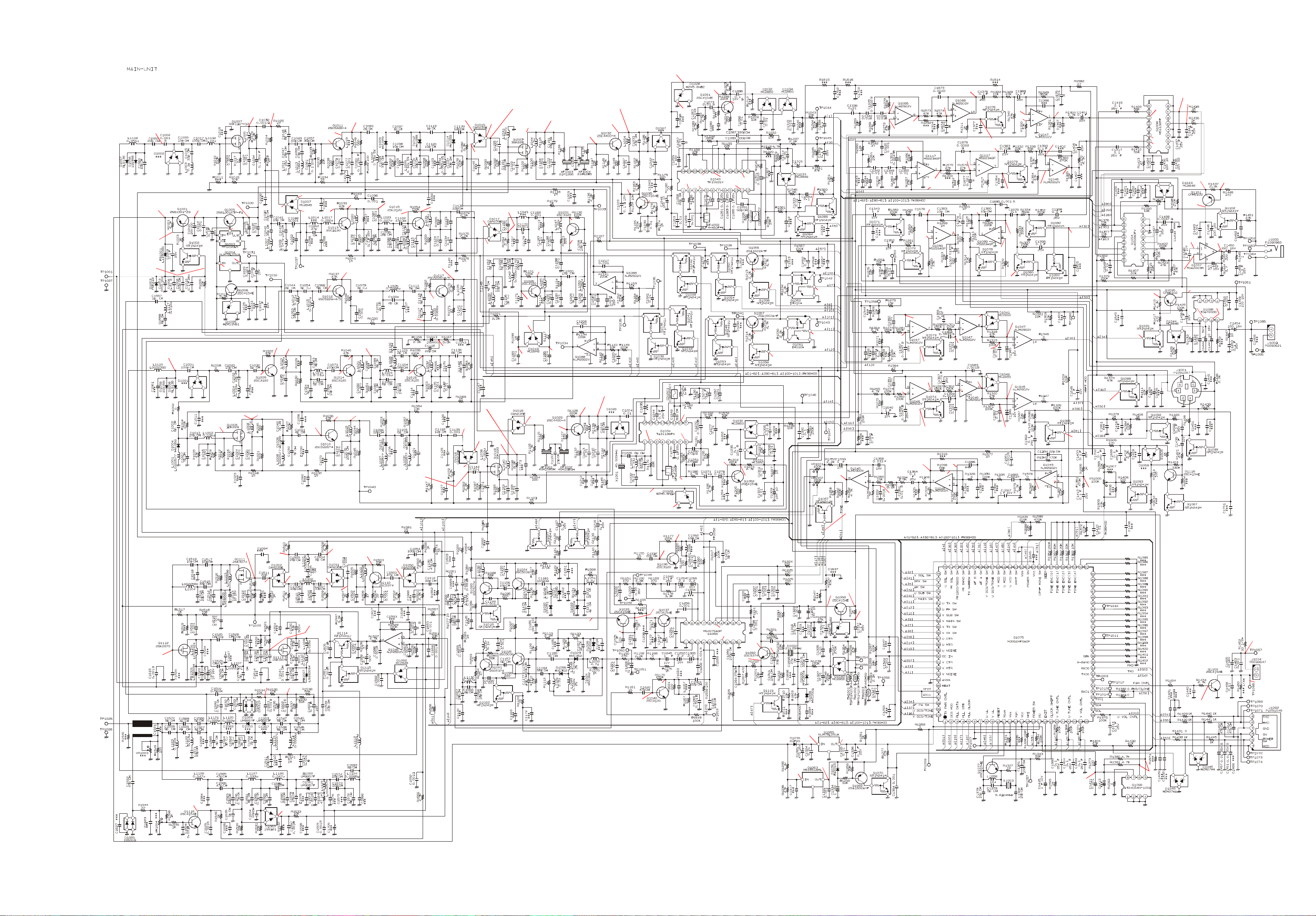
Circuit Diagram
MAIN Unit (Lot. 1~)
5.57V
(-9.3dBµ)
[-8.9dBµ]
13.8V
Power
ON:13.0V
OFF:13.8V
Power
ON:3.46V
OFF:0V
<-9.2dBµ>
{-6.4dBµ}
13.7V
3.93V
8.9V
4.87V
5.0V
(-3.7dBµ)
[-2.7dBµ]
7.44V
7.47V
1.69V
V Main 8.34V
V RX
7.7V
9.0V
5.85V
0.77V 0.51V
7.18V
<+9.4dBµ>
V Sub
0.76V
7.96V
SUB(U/U)
435.1MHz:+4.8dBµ
0.76V
4.85V
0.78V
(U/U)
435.1MHz:+21.0dBµ
7.3V
0.76V
5.95V
(+16.4dBµ)
5.87V
<+28.5dBµ>
SUB(V/V)
145.1MHz:+17.2dBµ
0.72V
4.01V
7.3V
6.78V
8.52V
0.67V
4.62V
V Main
4.56V
U Main
4.37V
(45.05MHZ):+16.0dBµ>
(U/U)435.1MHz(180.1MHz):+28.0dBµ
3.81V
U Sub
4.45V
Sub RX
U Sub
3.62V
4.48V
V Sub
4.38V
(V/V)145.1MHz(45.05MHz):+19.6dBµ
V Sub
4.34V
7.95V
(21.7MHZ):+16.0dBµ>
(U/U)435.1MHz(21.7MHz):+16.3dBµ
8.27V
6.23V
0.76V
Sub RX
7.4V
V Sub
8.08V
<45.05MHZ:+19.6dBµ>
7.19V
1.12V
(21.7MHZ):+18.4dBµ>
(U/U)435.1MHz(21.7MHz):+22.8dBµ
2.37V
1.22V
6.15V
0.72V
U Sub
8.09V
<45.05MHZ:+21.4dBµ>
(V/V)145.1MHz(45.05MHz):+21.0dBµ
3.39V
3.9V
4.94V
0.2V
5.5V
0.65V
5.6V
4.54V
5.49V
2.76V
5.32V
0.77V
2.72V
5.33V
1.5V
3.33V
(AM)
VHF RX:0V
VHF RX ON
“H”
UHF RX
0V
3.32V (AM)
0V (0)
UHF RX ON “H”
VHF TX
UHF TX
“H”
“H”
4.07V
4.04V
4.07V
2.14V
1.07V
4.06V
4.01V
4.06V
4.03V
1.94V
1.92V
2.22V
VHF DCS ON “H”
1.10V
UHF DCS ON “H”
1.93V
4.06V
4.01V
2.12V
1.06V
1.94V
2.23V
1.11V
4.06V
2.19V
SQL ON “H”
SQL ON “H”
1.94V
1.92V
VHF “L”, UHF “H”
1.10V
1.09V
1.93V
1.91V
2.21V
1.89V
1.91V
1.91V
1.89V
VHF “H”
UHF “L”
DTMF
TX “L”
PK SQL ON “H”
4.85V
8.92V
3.53V
8.36V
3.53V
VHF AFVR 0~4.73V
UHF AFVR 0~4.73V
13.75V
0V
1.34V
0.81V
6.36V
8.91V
0.49V 1.23V
13.33V
VHF TX(50W):2.35V
UHF TX(35W):2.50V
VHF TX(50W):2.10V
UHF TX(35W):3.00V
UHF TX(35W):4.00V UHF TX(35W):1.10V
1.95V
1.30V
2.10V
VHF TX(50W):2.1V
2.10V
UHF TX(35W):
2.55V
2.10V
1.35V
<45.05MHZ:+23.8dBµ>
(V/V)145.1MHz
(400.1MHz):+31.3dBµ
4.77V
3.27V
3.61V
7.33V
8.02V
0.47V
5.57V
8.86V
3.48V
5.6V
0.28V
3.72V
4.37V
0.71V
4.69V
4.83V
1.78V
2.78V
3.38V
2.28V
4.09V
4.95V
8.86V
TX NARROW ON “H”
5.95V
3.4V
4.06V
4.07V
3.92V
3.92V
4.01V
4.07V
FAN ON:0.77V
OFF:0V
FAN ON:11.93V
OFF:13.8V
FAN ON:0V
OFF:13.45V
VHF TX(50W):3.50V
UHF TX(35W):3.40V
VHF TX(50W):3.9V
(XX) = MAIN 145.1 MHz
[XX] = SUB 145.1 MHz
<XX> = MAIN 435.1 MHz
{XX} = SUB 435.1 MHz
8.45V
13.11V
5.22V
4.88V
4.88V
4.87V
17

MAIN Unit (Lot. 1~)
Note:
18
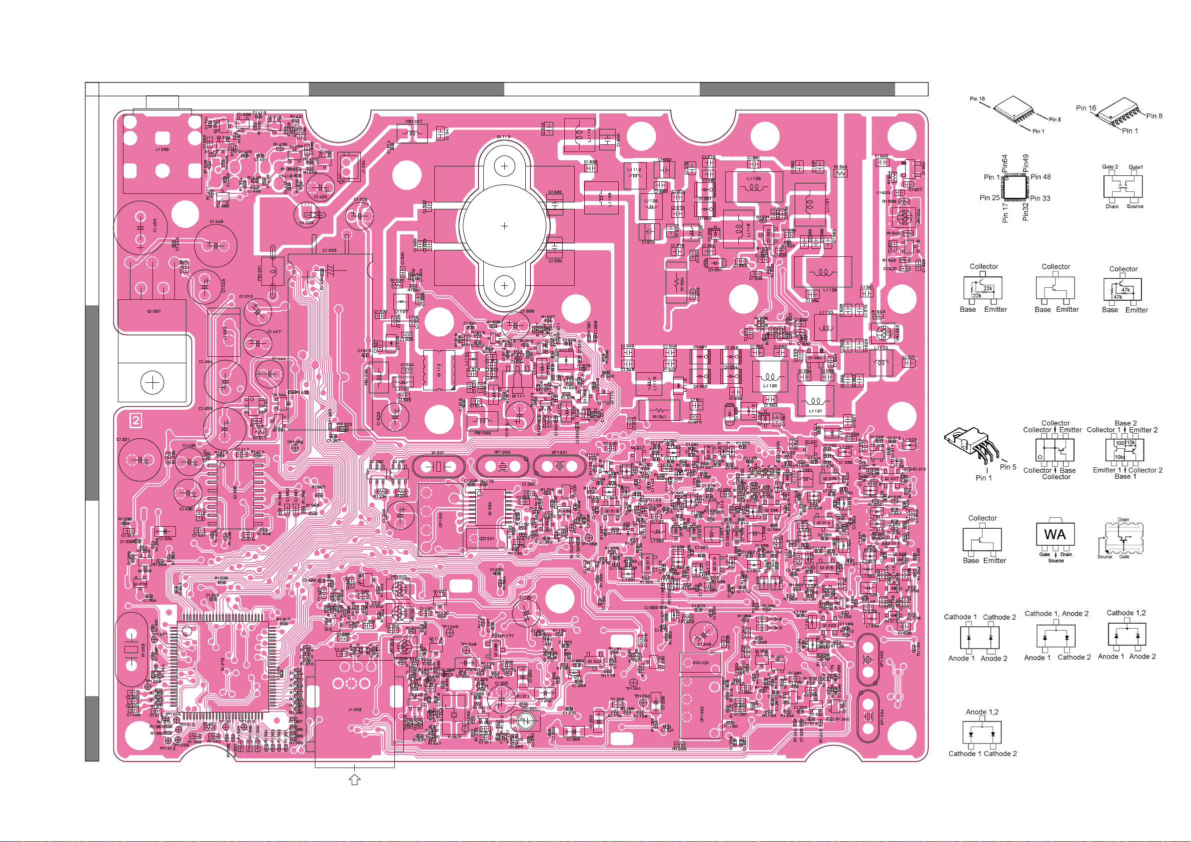
Parts Layout
MAIN Unit (Lot. 1~)
B
DCA
E
TA31136FN
(Q1034)
M51132FP
(Q1096)
1
3SK131 (V12)
M30620ECGP
(Q1075)
RT1N241M (N2)
(Q1027, 1030,
1064, 1066,
1067, 1070,
1085, 1086,
1087, 1091,
1092, 1093,
1099, 1115,
1119)
2
2SC3120 (HB)
(Q1009, 1013, 1014,
1015, 1016, 1038,
1040)
2SC5226 (R22)
(Q1012, 1017)
2SC4154E (LE)
(Q1051, 1052, 1116,
1118)
2SC5374 (NA)
(Q1060, 1110)
2SC5226-4
(Q1010, 1011)
(Q1007)
3SK228 (XR-)
(Q1008, 1019,
1023)
RT1P441U (P3)
(Q1042, 1114)
TDA2003H
(Q1097)
2SA1602A (MF)
(Q1069)
CPH6102 (AB)
(Q1095)
2SK3074 (WA)
(Q1111)
IMD10A (D10)
(Q1061, 1062)
2SK2975
(Q1112)
3
1SS319 (A4)
(D1064, 1065)
MC2850 (A7)
(D1030, 1031, 1032,
1034, 1040)
DAN235E
(D1015, 1016, 1018,
1051, 1052)
MC2848 (A6)
(D1062)
1SS321 (F9)
(D1063)
4
MC2846
(D1044)
Side A
19
MAIN Unit (Lot. 1~)
b
1
dca
e
BU4053BCFV
TK10931VT1
(Q1043)
M64076AGP
(Q1055)
NJM2902V
(Q1045, 1046, 1047, 1088)
2SB1201STP
(Q1005)
2SA1602A (MF)
(Q1056, 1057)
(Q1094)
BU4053BCFV-E2
(Q1094)
M5223AGP
(Q1089)
M5223AGP
(Q1117)
AT24C64N-10SI-1.8-SL722A
(Q1090)
TDA7233D
(Q1098)
2SB1301 (ZQ)
(Q1001)
2
RT1N241M (N2)
(Q1002, 1018, 1022,
1039, 1044, 1048,
1053, 1054, 1058,
1059, 1071, 1072,
1073, 1074, 1076,
1078, 1079, 1080,
1082, 1083, 1102)
2SC5374 (NA)
(Q1020, 1021)
2SC4154E (LE)
(Q1006, 1033,
1035, 1037, 1068,
1077, 1100)
2SC5006 (24)
(Q1024, 1025)
2SC3120 (HB)
(Q1026, 1031)
2SC4400 (RT4)
(Q1029, 1032)
M51951AML-600C (51)
(Q1063)
CNJM78L05UA (51)
(Q1004, 1065)
3
MM1216ENRE (1A)
(Q1003)
RT1P441U (P3)
(Q1036, 1041,
1049, 1050 )
CPH6102 (AB)
(Q1101)
20
MC2850 (A7)
(D1041, 1042)
4
Side B
HZM27WA (27A)
(D1045, 1046)
DAN235E
(D1017, 1050)
MC2848 (A6)
(D1007, 1019,
1033, 1043)
HZM11N
(D1005)
HZM5.6NB2 (562)
(D1028, 1029,
1038)
Circuit Diagram
MAIN Unit (Lot. 5~)
5.57V
(-9.3dBµ)
[-8.9dBµ]
13.8V
Power
ON:13.0V
OFF:13.8V
Power
ON:3.46V
OFF:0V
<-9.2dBµ>
{-6.4dBµ}
13.7V
3.93V
8.9V
4.87V
5.0V
9.0V
7.18V
7.44V
0.77V
(-3.7dBµ)
[-2.7dBµ]
V RX
7.7V
5.85V
<+9.4dBµ>
7.47V
1.69V
V Main 8.34V
V Sub
0.76V
7.96V
SUB(U/U)
435.1MHz:+4.8dBµ
0.76V
(+16.4dBµ)
5.87V
4.85V
0.78V
(U/U)
435.1MHz:+21.0dBµ
0.76V
5.95V
7.3V
<+28.5dBµ>
SUB(V/V)
145.1MHz:+17.2dBµ
0.72V
7.3V
0.51V
6.78V
8.52V
0.67V
4.01V
4.62V
V Main
4.56V
U Main
4.37V
(45.05MHZ):+16.0dBµ>
(U/U)435.1MHz(180.1MHz):+28.0dBµ
3.81V
U Sub
4.45V
Sub RX
U Sub
3.62V
4.48V
V Sub
4.38V
V Sub
4.34V
(21.7MHZ):+16.0dBµ>
(U/U)435.1MHz(21.7MHz):+16.3dBµ
8.27V
0.76V
Sub RX
7.4V
V Sub
8.08V
7.19V
7.95V
(21.7MHZ):+18.4dBµ>
(U/U)435.1MHz(21.7MHz):+22.8dBµ
1.22V
6.15V
0.72V
6.23V
U Sub
8.09V
<45.05MHZ:+21.4dBµ>
(V/V)145.1MHz(45.05MHz):+21.0dBµ
3.39V
1.12V
2.37V
3.9V
4.94V
0.2V
5.5V
0.65V
5.6V
4.54V
5.49V
2.76V
5.32V
0.77V
2.72V
5.33V
1.5V
3.33V
(AM)
VHF RX:0V
VHF RX ON
“H”
UHF RX
0V
3.32V (AM)
0V (0)
UHF RX ON “H”
VHF TX
UHF TX
“H”
“H”
4.07V
4.04V
2.14V
1.07V
4.07V
4.06V
4.01V
4.06V
1.94V
1.92V
2.22V
VHF DCS ON “H”
1.10V
UHF DCS ON “H”
4.03V
1.93V
4.06V
4.01V
2.12V
1.06V
1.94V
2.23V
1.11V
4.06V
2.19V
SQL ON “H”
SQL ON “H”
1.94V
1.92V
VHF “L”, UHF “H”
1.10V
1.09V
1.93V
1.91V
2.21V
1.89V
1.91V
1.91V
1.89V
VHF “H”
UHF “L”
DTMF
TX “L”
PK SQL ON “H”
4.85V
8.92V
3.53V
8.36V
3.53V
VHF AFVR 0~4.73V
UHF AFVR 0~4.73V
13.75V
0V
1.34V
0.81V
6.36V
8.91V
0.49V 1.23V
13.33V
VHF TX(50W):2.35V
UHF TX(35W):2.50V
VHF TX(50W):2.10V
UHF TX(35W):3.00V
UHF TX(35W):4.00V UHF TX(35W):1.10V
1.95V
1.30V
2.10V
VHF TX(50W):2.1V
2.10V
UHF TX(35W):
2.55V
2.10V
1.35V
<45.05MHZ:+23.8dBµ>
(V/V)145.1MHz
(400.1MHz):+31.3dBµ
4.77V
3.27V
3.61V
(V/V)145.1MHz(45.05MHz):+19.6dBµ
<45.05MHZ:+19.6dBµ>
7.33V
8.02V
0.47V
5.57V
8.86V
3.48V
5.6V
0.28V
3.72V
4.37V
0.71V
4.69V
4.83V
1.78V
2.78V
3.38V
2.28V
4.09V
TX NARROW ON “H”
8.86V
4.95V
5.95V
3.4V
4.06V
4.07V
3.92V
3.92V
4.01V
4.07V
FAN ON:0.77V
OFF:0V
FAN ON:11.93V
OFF:13.8V
FAN ON:0V
OFF:13.45V
VHF TX(50W):3.50V
UHF TX(35W):3.40V
VHF TX(50W):3.9V
(XX) = MAIN 145.1 MHz
[XX] = SUB 145.1 MHz
<XX> = MAIN 435.1 MHz
{XX} = SUB 435.1 MHz
8.45V
13.11V
5.22V
4.88V
4.88V
4.87V
21
 Loading...