

Page 1

LogiCORE™ IP
SPI-4.2 Lite v4.3
User Guide
UG181 June 27, 2008
R
Page 2
R
Xilinx is disclosing this Document and Intellectual Property (hereinafter “the Design”) to you for use in the development of designs to operate
on, or interface with Xilinx FPGAs. Except as stated herein, none of the Design may be copied, reproduced, distributed, republished,
downloaded, displayed, posted, or transmitted in any form or by any means including, but not limited to, electronic, mechanical,
photocopying, recording, or otherwise, without the prior written consent of Xilinx. Any unauthorized use of the Design may violate copyright
laws, trademark laws, the laws of privacy and publicity, and communications regulations and statutes.
Xilinx does not assume any liability arising out of the application or use of the Design; nor does Xilinx convey any license under its patents,
copyrights, or any rights of others. You are responsible for obtaining any rights you may require for your use or implementation of the Design.
Xilinx reserves the right to make changes, at any time, to the Design as deemed desirable in the sole discretion of Xilinx. Xilinx assumes no
obligation to correct any errors contained herein or to advise you of any correction if such be made. Xilinx will not assume any liability for the
accuracy or correctness of any engineering or technical support or assistance provided to you in connection with the Design.
THE DESIGN IS PROVIDED “AS IS” WITH ALL FAULTS, AND THE ENTIRE RISK AS TO ITS FUNCTION AND IMPLEMENTATION IS
WITH YOU. YOU ACKNOWLEDGE AND AGREE THAT YOU HAVE NOT RELIED ON ANY ORAL OR WRITTEN INFORMATION OR
ADVICE, WHETHER GIVEN BY XILINX, OR ITS AGENTS OR EMPLOYEES. XILINX MAKES NO OTHER WARRANTIES, WHETHER
EXPRESS, IMPLIED, OR STATUTORY, REGARDING THE DESIGN, INCLUDING ANY WARRANTIES OF MERCHANTABILITY, FITNESS
FOR A PARTICULAR PURPOSE, TITLE, AND NONINFRINGEMENT OF THIRD-PARTY RIGHTS.
IN NO EVENT WILL XILINX BE LIABLE FOR ANY CONSEQUENTIAL, INDIRECT, EXEMPLARY, SPECIAL, OR INCIDENTAL DAMAGES,
INCLUDING ANY LOST DATA AND LOST PROFITS, ARISING FROM OR RELATING TO YOUR USE OF THE DESIGN, EVEN IF YOU
HAVE BEEN ADVISED OF THE POSSIBILITY OF SUCH DAMAGES. THE TOTAL CUMULATIVE LIABILITY OF XILINX IN CONNECTION
WITH YOUR USE OF THE DESIGN, WHETHER IN CONTRACT OR TORT OR OTHERWISE, WILL IN NO EVENT EXCEED THE
AMOUNT OF FEES PAID BY YOU TO XILINX HEREUNDER FOR USE OF THE DESIGN. YOU ACKNOWLEDGE THAT THE FEES, IF
ANY, REFLECT THE ALLOCATION OF RISK SET FORTH IN THIS AGREEMENT AND THAT XILINX WOULD NOT MAKE AVAILABLE
THE DESIGN TO YOU WITHOUT THESE LIMITATIONS OF LIABILITY.
The Design is not designed or intended for use in the development of on-line control equipment in hazardous environments requiring failsafe controls, such as in the operation of nuclear facilities, aircraft navigation or communications systems, air traffic control, life support, or
weapons systems (“High-Risk Applications”). Xilinx specifically disclaims any express or implied warranties of fitness for such High-Risk
Applications. You represent that use of the Design in such High-Risk Applications is fully at your risk.
© 2005-2008 Xilinx, Inc. All rights reserved. XILINX, the Xilinx logo, and other designated brands included herein are trademarks of Xilinx,
Inc. All other trademarks are the property of their respective owners.
SPI-4.2 Lite v4.3 User Guide
UG181 June 27, 2008
The following table shows the revision history for this document.
Date Version Revision
8/31/05 1.1 Initial Xilinx release.
1/18/06 1.2 Updated release version, tool version, and release date.
7/13/06 2.0 Updated version to 4.1, release date, ISE to v8.2i.
2/15/07 3.0 Updated version to 4.2, ISE to v9.1i, added Virtex-3E support.
4/02/07 3.1 Added support for Spartan-3A DSP devices.
4/16/08 4.0 Updated for ISE v10.1.
6/27/08 4.5 Updated the ISE v10.1 SP1 release.
SPI-4.2 Lite v4.3 User Guide www.xilinx.com
UG181 June 27, 2008
Page 3

Table of Contents
Preface: About This Guide
Contents . . . . . . . . . . . . . . . . . . . . . . . . . . . . . . . . . . . . . . . . . . . . . . . . . . . . . . . . . . . . . . . . . . . . 11
Conventions . . . . . . . . . . . . . . . . . . . . . . . . . . . . . . . . . . . . . . . . . . . . . . . . . . . . . . . . . . . . . . . . 12
Typographical. . . . . . . . . . . . . . . . . . . . . . . . . . . . . . . . . . . . . . . . . . . . . . . . . . . . . . . . . . . . 12
Online Document . . . . . . . . . . . . . . . . . . . . . . . . . . . . . . . . . . . . . . . . . . . . . . . . . . . . . . . . . 13
Chapter 1: Introduction
About the Core. . . . . . . . . . . . . . . . . . . . . . . . . . . . . . . . . . . . . . . . . . . . . . . . . . . . . . . . . . . . . . 15
Recommended Design Experience. . . . . . . . . . . . . . . . . . . . . . . . . . . . . . . . . . . . . . . . . . . 15
Additional Core Resources . . . . . . . . . . . . . . . . . . . . . . . . . . . . . . . . . . . . . . . . . . . . . . . . . . 15
Technical Support. . . . . . . . . . . . . . . . . . . . . . . . . . . . . . . . . . . . . . . . . . . . . . . . . . . . . . . . . . . 16
Feedback. . . . . . . . . . . . . . . . . . . . . . . . . . . . . . . . . . . . . . . . . . . . . . . . . . . . . . . . . . . . . . . . . . . . 16
SPI-4.2 Lite Core . . . . . . . . . . . . . . . . . . . . . . . . . . . . . . . . . . . . . . . . . . . . . . . . . . . . . . . . . . 16
Document . . . . . . . . . . . . . . . . . . . . . . . . . . . . . . . . . . . . . . . . . . . . . . . . . . . . . . . . . . . . . . . 16
Chapter 2: Core Architecture
System Overview . . . . . . . . . . . . . . . . . . . . . . . . . . . . . . . . . . . . . . . . . . . . . . . . . . . . . . . . . . . 17
Sink Core . . . . . . . . . . . . . . . . . . . . . . . . . . . . . . . . . . . . . . . . . . . . . . . . . . . . . . . . . . . . . . . . 18
Source Core . . . . . . . . . . . . . . . . . . . . . . . . . . . . . . . . . . . . . . . . . . . . . . . . . . . . . . . . . . . . . . 18
Sink Core Interfaces. . . . . . . . . . . . . . . . . . . . . . . . . . . . . . . . . . . . . . . . . . . . . . . . . . . . . . . . . 19
Sink SPI-4.2 Interface . . . . . . . . . . . . . . . . . . . . . . . . . . . . . . . . . . . . . . . . . . . . . . . . . . . . . . 21
Sink User Interface . . . . . . . . . . . . . . . . . . . . . . . . . . . . . . . . . . . . . . . . . . . . . . . . . . . . . . . . 22
Source Core Interfaces . . . . . . . . . . . . . . . . . . . . . . . . . . . . . . . . . . . . . . . . . . . . . . . . . . . . . . 30
Source SPI-4.2 Interface . . . . . . . . . . . . . . . . . . . . . . . . . . . . . . . . . . . . . . . . . . . . . . . . . . . . 31
Source User Interface. . . . . . . . . . . . . . . . . . . . . . . . . . . . . . . . . . . . . . . . . . . . . . . . . . . . . . 32
Chapter 3: Generating the Core
CORE Generator Graphical User Interface . . . . . . . . . . . . . . . . . . . . . . . . . . . . . . . . . . . 43
Main Screen . . . . . . . . . . . . . . . . . . . . . . . . . . . . . . . . . . . . . . . . . . . . . . . . . . . . . . . . . . . . . . . . 44
Sink Status Options Screen. . . . . . . . . . . . . . . . . . . . . . . . . . . . . . . . . . . . . . . . . . . . . . . . . . 44
Calendar . . . . . . . . . . . . . . . . . . . . . . . . . . . . . . . . . . . . . . . . . . . . . . . . . . . . . . . . . . . . . . . . 45
Flow Control . . . . . . . . . . . . . . . . . . . . . . . . . . . . . . . . . . . . . . . . . . . . . . . . . . . . . . . . . . . . . 45
Status Interface . . . . . . . . . . . . . . . . . . . . . . . . . . . . . . . . . . . . . . . . . . . . . . . . . . . . . . . . . . . 45
Sink Other Options Screen . . . . . . . . . . . . . . . . . . . . . . . . . . . . . . . . . . . . . . . . . . . . . . . . . . 46
Synchronization . . . . . . . . . . . . . . . . . . . . . . . . . . . . . . . . . . . . . . . . . . . . . . . . . . . . . . . . . . 46
FIFO Threshold. . . . . . . . . . . . . . . . . . . . . . . . . . . . . . . . . . . . . . . . . . . . . . . . . . . . . . . . . . . 46
Clocking. . . . . . . . . . . . . . . . . . . . . . . . . . . . . . . . . . . . . . . . . . . . . . . . . . . . . . . . . . . . . . . . . 47
Source Status Options Screen . . . . . . . . . . . . . . . . . . . . . . . . . . . . . . . . . . . . . . . . . . . . . . . 47
Calendar . . . . . . . . . . . . . . . . . . . . . . . . . . . . . . . . . . . . . . . . . . . . . . . . . . . . . . . . . . . . . . . . 47
Status Interface . . . . . . . . . . . . . . . . . . . . . . . . . . . . . . . . . . . . . . . . . . . . . . . . . . . . . . . . . . . 48
Synchronization . . . . . . . . . . . . . . . . . . . . . . . . . . . . . . . . . . . . . . . . . . . . . . . . . . . . . . . . . . 48
Source Other Options Screen . . . . . . . . . . . . . . . . . . . . . . . . . . . . . . . . . . . . . . . . . . . . . . . . 48
SPI-4.2 Lite v4.3 User Guide www.xilinx.com
UG181 June 27, 2008
Page 4

Bursting . . . . . . . . . . . . . . . . . . . . . . . . . . . . . . . . . . . . . . . . . . . . . . . . . . . . . . . . . . . . . . . . . 48
FIFO Threshold. . . . . . . . . . . . . . . . . . . . . . . . . . . . . . . . . . . . . . . . . . . . . . . . . . . . . . . . . . . 49
Clocking. . . . . . . . . . . . . . . . . . . . . . . . . . . . . . . . . . . . . . . . . . . . . . . . . . . . . . . . . . . . . . . . . 49
Calendar COE File Format. . . . . . . . . . . . . . . . . . . . . . . . . . . . . . . . . . . . . . . . . . . . . . . . . . . 50
Chapter 4: Designing with the Core
General Design Guidelines . . . . . . . . . . . . . . . . . . . . . . . . . . . . . . . . . . . . . . . . . . . . . . . . . 51
Know the Degree of Difficulty . . . . . . . . . . . . . . . . . . . . . . . . . . . . . . . . . . . . . . . . . . . . . . 51
Understand Signal Pipelining . . . . . . . . . . . . . . . . . . . . . . . . . . . . . . . . . . . . . . . . . . . . . . 51
Keep it Registered . . . . . . . . . . . . . . . . . . . . . . . . . . . . . . . . . . . . . . . . . . . . . . . . . . . . . . . . 52
Recognize Timing Critical Signals . . . . . . . . . . . . . . . . . . . . . . . . . . . . . . . . . . . . . . . . . . . 52
Use Supported Design Flows . . . . . . . . . . . . . . . . . . . . . . . . . . . . . . . . . . . . . . . . . . . . . . . 52
Make Only Allowed Modifications . . . . . . . . . . . . . . . . . . . . . . . . . . . . . . . . . . . . . . . . . . 52
Initializing the SPI-4.2 Lite Core. . . . . . . . . . . . . . . . . . . . . . . . . . . . . . . . . . . . . . . . . . . . . 52
Sink Core . . . . . . . . . . . . . . . . . . . . . . . . . . . . . . . . . . . . . . . . . . . . . . . . . . . . . . . . . . . . . . . . . . . 53
Basic Operation . . . . . . . . . . . . . . . . . . . . . . . . . . . . . . . . . . . . . . . . . . . . . . . . . . . . . . . . . . 53
SPI-4.2 Interface . . . . . . . . . . . . . . . . . . . . . . . . . . . . . . . . . . . . . . . . . . . . . . . . . . . . . . . . . . 53
Sink User Interface . . . . . . . . . . . . . . . . . . . . . . . . . . . . . . . . . . . . . . . . . . . . . . . . . . . . . . . . 58
Sink Static Configuration Signals . . . . . . . . . . . . . . . . . . . . . . . . . . . . . . . . . . . . . . . . . . . 67
Sink Data Capture Implementation . . . . . . . . . . . . . . . . . . . . . . . . . . . . . . . . . . . . . . . . . 69
Synchronization and Start-up . . . . . . . . . . . . . . . . . . . . . . . . . . . . . . . . . . . . . . . . . . . . . . 70
Error Handling . . . . . . . . . . . . . . . . . . . . . . . . . . . . . . . . . . . . . . . . . . . . . . . . . . . . . . . . . . . 72
Source Core . . . . . . . . . . . . . . . . . . . . . . . . . . . . . . . . . . . . . . . . . . . . . . . . . . . . . . . . . . . . . . . . . 76
Basic Operation . . . . . . . . . . . . . . . . . . . . . . . . . . . . . . . . . . . . . . . . . . . . . . . . . . . . . . . . . . 76
Source SPI-4.2 Interface . . . . . . . . . . . . . . . . . . . . . . . . . . . . . . . . . . . . . . . . . . . . . . . . . . . . 76
Source User Interface. . . . . . . . . . . . . . . . . . . . . . . . . . . . . . . . . . . . . . . . . . . . . . . . . . . . . . 82
Source Static Configuration Signals . . . . . . . . . . . . . . . . . . . . . . . . . . . . . . . . . . . . . . . . . 93
Synchronization and Start-up . . . . . . . . . . . . . . . . . . . . . . . . . . . . . . . . . . . . . . . . . . . . . . 94
Error Handling . . . . . . . . . . . . . . . . . . . . . . . . . . . . . . . . . . . . . . . . . . . . . . . . . . . . . . . . . . . 96
Chapter 5: Constraining the Core
Overview . . . . . . . . . . . . . . . . . . . . . . . . . . . . . . . . . . . . . . . . . . . . . . . . . . . . . . . . . . . . . . . . . . . 99
Sink Core Required Constraints . . . . . . . . . . . . . . . . . . . . . . . . . . . . . . . . . . . . . . . . . . . . . 99
Timing Constraints . . . . . . . . . . . . . . . . . . . . . . . . . . . . . . . . . . . . . . . . . . . . . . . . . . . . . . . 99
DCM and Static Alignment Constraints . . . . . . . . . . . . . . . . . . . . . . . . . . . . . . . . . . . . . 101
Placement Constraints . . . . . . . . . . . . . . . . . . . . . . . . . . . . . . . . . . . . . . . . . . . . . . . . . . . . 102
Sink Core Optional Constraints . . . . . . . . . . . . . . . . . . . . . . . . . . . . . . . . . . . . . . . . . . . . 103
IDelayCtrl . . . . . . . . . . . . . . . . . . . . . . . . . . . . . . . . . . . . . . . . . . . . . . . . . . . . . . . . . . . . . . 103
I/O Standards Constraints . . . . . . . . . . . . . . . . . . . . . . . . . . . . . . . . . . . . . . . . . . . . . . . . 103
Area Group Constraints . . . . . . . . . . . . . . . . . . . . . . . . . . . . . . . . . . . . . . . . . . . . . . . . . . 104
Timing Ignore Constraints . . . . . . . . . . . . . . . . . . . . . . . . . . . . . . . . . . . . . . . . . . . . . . . . 104
Source Core Required Constraints . . . . . . . . . . . . . . . . . . . . . . . . . . . . . . . . . . . . . . . . . . 104
Timing Constraints . . . . . . . . . . . . . . . . . . . . . . . . . . . . . . . . . . . . . . . . . . . . . . . . . . . . . . 104
Placement Constraints . . . . . . . . . . . . . . . . . . . . . . . . . . . . . . . . . . . . . . . . . . . . . . . . . . . . 105
Source Core Optional Constraints . . . . . . . . . . . . . . . . . . . . . . . . . . . . . . . . . . . . . . . . . . 107
I/O Standards Constraints . . . . . . . . . . . . . . . . . . . . . . . . . . . . . . . . . . . . . . . . . . . . . . . . 107
Area Group Constraints . . . . . . . . . . . . . . . . . . . . . . . . . . . . . . . . . . . . . . . . . . . . . . . . . . 107
Timing Ignore Constraints . . . . . . . . . . . . . . . . . . . . . . . . . . . . . . . . . . . . . . . . . . . . . . . . 108
User Constraints . . . . . . . . . . . . . . . . . . . . . . . . . . . . . . . . . . . . . . . . . . . . . . . . . . . . . . . . . . . 108
www.xilinx.com SPI-4.2 Lite v4.3 User Guide
UG181 June 27, 2008
Page 5

Constraints Migration . . . . . . . . . . . . . . . . . . . . . . . . . . . . . . . . . . . . . . . . . . . . . . . . . . . . . . 108
New Target Region or Device Package. . . . . . . . . . . . . . . . . . . . . . . . . . . . . . . . . . . . . . 108
Modifying the UCF File. . . . . . . . . . . . . . . . . . . . . . . . . . . . . . . . . . . . . . . . . . . . . . . . . . . 109
Chapter 6: Special Design Considerations
Sink Clocking Options . . . . . . . . . . . . . . . . . . . . . . . . . . . . . . . . . . . . . . . . . . . . . . . . . . . . . 111
Embedded Clocking . . . . . . . . . . . . . . . . . . . . . . . . . . . . . . . . . . . . . . . . . . . . . . . . . . . . . 111
User Clocking . . . . . . . . . . . . . . . . . . . . . . . . . . . . . . . . . . . . . . . . . . . . . . . . . . . . . . . . . . . 112
Source Clocking Options . . . . . . . . . . . . . . . . . . . . . . . . . . . . . . . . . . . . . . . . . . . . . . . . . . . 115
Master Clocking . . . . . . . . . . . . . . . . . . . . . . . . . . . . . . . . . . . . . . . . . . . . . . . . . . . . . . . . . 116
Slave Clocking . . . . . . . . . . . . . . . . . . . . . . . . . . . . . . . . . . . . . . . . . . . . . . . . . . . . . . . . . . 119
Multiple Core Implementations . . . . . . . . . . . . . . . . . . . . . . . . . . . . . . . . . . . . . . . . . . . . 120
Instantiating Multiple Cores. . . . . . . . . . . . . . . . . . . . . . . . . . . . . . . . . . . . . . . . . . . . . . . 120
Generating the Cores . . . . . . . . . . . . . . . . . . . . . . . . . . . . . . . . . . . . . . . . . . . . . . . . . . . . . 121
Creating Top-Level UCF File . . . . . . . . . . . . . . . . . . . . . . . . . . . . . . . . . . . . . . . . . . . . . . 121
Clocking Considerations . . . . . . . . . . . . . . . . . . . . . . . . . . . . . . . . . . . . . . . . . . . . . . . . . . 122
Chapter 7: Simulating and Implementing the Core
Functional Simulation. . . . . . . . . . . . . . . . . . . . . . . . . . . . . . . . . . . . . . . . . . . . . . . . . . . . . . 125
Generating a Simulation Model . . . . . . . . . . . . . . . . . . . . . . . . . . . . . . . . . . . . . . . . . . . . 125
Timing Simulation . . . . . . . . . . . . . . . . . . . . . . . . . . . . . . . . . . . . . . . . . . . . . . . . . . . . . . . 126
Synthesis . . . . . . . . . . . . . . . . . . . . . . . . . . . . . . . . . . . . . . . . . . . . . . . . . . . . . . . . . . . . . . . . . . 127
Synthesis of Example Design . . . . . . . . . . . . . . . . . . . . . . . . . . . . . . . . . . . . . . . . . . . . . . 127
Xilinx Tool Flow . . . . . . . . . . . . . . . . . . . . . . . . . . . . . . . . . . . . . . . . . . . . . . . . . . . . . . . . . . . 128
Example Design Script . . . . . . . . . . . . . . . . . . . . . . . . . . . . . . . . . . . . . . . . . . . . . . . . . . . 128
NGDBuild . . . . . . . . . . . . . . . . . . . . . . . . . . . . . . . . . . . . . . . . . . . . . . . . . . . . . . . . . . . . . . 128
Mapping the Design . . . . . . . . . . . . . . . . . . . . . . . . . . . . . . . . . . . . . . . . . . . . . . . . . . . . . 128
Place and Route . . . . . . . . . . . . . . . . . . . . . . . . . . . . . . . . . . . . . . . . . . . . . . . . . . . . . . . . . 128
Static Timing Analysis. . . . . . . . . . . . . . . . . . . . . . . . . . . . . . . . . . . . . . . . . . . . . . . . . . . . 129
Timing Simulation . . . . . . . . . . . . . . . . . . . . . . . . . . . . . . . . . . . . . . . . . . . . . . . . . . . . . . . 129
Generating a Bitstream . . . . . . . . . . . . . . . . . . . . . . . . . . . . . . . . . . . . . . . . . . . . . . . . . . . 129
Appendix A: SPI-4.2 Lite Control Word
Appendix B: SPI-4.2 Lite Calendar Programming
Overview . . . . . . . . . . . . . . . . . . . . . . . . . . . . . . . . . . . . . . . . . . . . . . . . . . . . . . . . . . . . . . . . . . 133
Example 1 . . . . . . . . . . . . . . . . . . . . . . . . . . . . . . . . . . . . . . . . . . . . . . . . . . . . . . . . . . . . . . . . . . 133
Example 2 . . . . . . . . . . . . . . . . . . . . . . . . . . . . . . . . . . . . . . . . . . . . . . . . . . . . . . . . . . . . . . . . . . 133
Example 3 . . . . . . . . . . . . . . . . . . . . . . . . . . . . . . . . . . . . . . . . . . . . . . . . . . . . . . . . . . . . . . . . . . 134
Appendix C: SPI-4.2 Lite Core Verification
SPI-4.2 Lite v4.3 User Guide www.xilinx.com
UG181 June 27, 2008
Page 6

www.xilinx.com SPI-4.2 Lite v4.3 User Guide
UG181 June 27, 2008
Page 7

Schedule of Figures
Chapter 2: Core Architecture
Figure 2-1: SPI-4.2 Lite Core in a Typical Link Layer Application. . . . . . . . . . . . . . . . . . . 18
Figure 2-2: Sink Core Block Diagram. . . . . . . . . . . . . . . . . . . . . . . . . . . . . . . . . . . . . . . . . . . . 20
Figure 2-3: Source Core Block Diagram and I/O Interface Signals . . . . . . . . . . . . . . . . . . 31
Chapter 3: Generating the Core
Figure 3-1: SPI-4.2 Lite Sink and Source Main Customization Screen . . . . . . . . . . . . . . . 44
Chapter 4: Designing with the Core
Figure 4-1: SPI-4.2 Interface to the 64-Bit User Interface . . . . . . . . . . . . . . . . . . . . . . . . . . . 54
Figure 4-2: Sink Data Path - Short Packet Transfers with Minimum SOP Spacing
Enforced. . . . . . . . . . . . . . . . . . . . . . . . . . . . . . . . . . . . . . . . . . . . . . . . . . . . . . . . . . . . . . . . . . . 55
Figure 4-3: Sink Training Valid Status . . . . . . . . . . . . . . . . . . . . . . . . . . . . . . . . . . . . . . . . . . 59
Figure 4-4: Sink FIFO Almost Empty . . . . . . . . . . . . . . . . . . . . . . . . . . . . . . . . . . . . . . . . . . . . 60
Figure 4-5: Sink FIFO Empty . . . . . . . . . . . . . . . . . . . . . . . . . . . . . . . . . . . . . . . . . . . . . . . . . . . 60
Figure 4-6: Status FIFO Calendar and Status Memory Block Diagram. . . . . . . . . . . . . . . 62
Figure 4-7: Sink Calendar Initialization . . . . . . . . . . . . . . . . . . . . . . . . . . . . . . . . . . . . . . . . . 63
Figure 4-8: Typical Flow Control Implementation for 4-Channel System . . . . . . . . . . . . 64
Figure 4-9: Sink Status FIFO Interface Example 1: 10-channel Configuration. . . . . . . . . 65
Figure 4-10: Sink Status FIFO Interface Example: 64-channel Configuration . . . . . . . . . 66
Figure 4-11: Sink Status Path - User Interface to SPI-4.2 Interface. . . . . . . . . . . . . . . . . . . 67
Figure 4-12: FIFO Almost Full Mode “00” . . . . . . . . . . . . . . . . . . . . . . . . . . . . . . . . . . . . . . . . 68
Figure 4-13: FIFO Almost Full Mode “01” . . . . . . . . . . . . . . . . . . . . . . . . . . . . . . . . . . . . . . . . 68
Figure 4-14: FIFO Almost Full Mode “10” or “11” . . . . . . . . . . . . . . . . . . . . . . . . . . . . . . . . . 69
Figure 4-15: Sink Startup Sequence State Machine. . . . . . . . . . . . . . . . . . . . . . . . . . . . . . . . 71
Figure 4-16: Short Packet Support. . . . . . . . . . . . . . . . . . . . . . . . . . . . . . . . . . . . . . . . . . . . . . . 73
Figure 4-17: Sequential Payload Control Word Example . . . . . . . . . . . . . . . . . . . . . . . . . . . 74
Figure 4-18: Example of Error Flag SnkFFDIP4Err . . . . . . . . . . . . . . . . . . . . . . . . . . . . . . . . 75
Figure 4-19: Example of Error Flag SnkFFDIP4Err and SnkFFPayloadDIP4 . . . . . . . . . . 75
Figure 4-20: Example of Error Flag SnkFFPayloadErr. . . . . . . . . . . . . . . . . . . . . . . . . . . . . . 76
Figure 4-21: Source Data Path: User Interface to SPI-4.2 Interface. . . . . . . . . . . . . . . . . . . 77
Figure 4-22: Source Data Path - Minimum SOP Spacing Enforced . . . . . . . . . . . . . . . . . . 78
Figure 4-23: Source Data Path - Short Packet Transfers . . . . . . . . . . . . . . . . . . . . . . . . . . . . 78
Figure 4-24: Source FIFO Almost-full Condition. . . . . . . . . . . . . . . . . . . . . . . . . . . . . . . . . . 84
Figure 4-25: Source FIFO Overflow Condition. . . . . . . . . . . . . . . . . . . . . . . . . . . . . . . . . . . . 84
Figure 4-26: Writing to the Source FIFO . . . . . . . . . . . . . . . . . . . . . . . . . . . . . . . . . . . . . . . . . 85
Figure 4-27: Typical User Design Example . . . . . . . . . . . . . . . . . . . . . . . . . . . . . . . . . . . . . . . 86
Figure 4-28: Source Calendar Initialization. . . . . . . . . . . . . . . . . . . . . . . . . . . . . . . . . . . . . . . 87
Figure 4-29: Addressable Status FIFO Interface. . . . . . . . . . . . . . . . . . . . . . . . . . . . . . . . . . . 88
Page 8

Figure 4-30: Addressable Status FIFO Interface: 4-Channel Configuration . . . . . . . . . . . 89
Figure 4-31: Addressable Status FIFO Interface: 256-channel configuration . . . . . . . . . . 90
Figure 4-32: Addressable Status FIFO Interface - SPI-4.2 Interface to User Interface . . 91
Figure 4-33: Transparent Status FIFO Interface Block Diagram . . . . . . . . . . . . . . . . . . . . . 92
Figure 4-34: Transparent Source Status FIFO Interface: 256-channel Configuration . . . 93
Figure 4-35: Example Of Source Burst Mode = 0 . . . . . . . . . . . . . . . . . . . . . . . . . . . . . . . . . . 94
Figure 4-36: Example Of Source Burst Mode = 1 . . . . . . . . . . . . . . . . . . . . . . . . . . . . . . . . . . 94
Figure 4-37: Source Startup Sequence State Machine. . . . . . . . . . . . . . . . . . . . . . . . . . . . . . 95
Chapter 6: Special Design Considerations
Figure 6-1: Embedded Clocking Option . . . . . . . . . . . . . . . . . . . . . . . . . . . . . . . . . . . . . . . . 112
Figure 6-2: Example: Sink User Clocking Inputs . . . . . . . . . . . . . . . . . . . . . . . . . . . . . . . . . 113
Figure 6-3: Sink User Clocking: Global Clocking . . . . . . . . . . . . . . . . . . . . . . . . . . . . . . . . 114
Figure 6-4: Sink User Clocking: Regional Clocking . . . . . . . . . . . . . . . . . . . . . . . . . . . . . . 115
Figure 6-5: Source Clocking: Master and Slave Implementation . . . . . . . . . . . . . . . . . . . 116
Figure 6-6: Source Clocking: Global Clocking for SysClk. . . . . . . . . . . . . . . . . . . . . . . . . 117
Figure 6-7: Source Clocking: Global Clocking for TSClk . . . . . . . . . . . . . . . . . . . . . . . . . 117
Figure 6-8: Source Clocking: Regional Clocking for SysClk. . . . . . . . . . . . . . . . . . . . . . . 118
Figure 6-9: Source Clocking: Regional Clocking for TSClk . . . . . . . . . . . . . . . . . . . . . . . 118
Figure 6-10: Slave Clocking Inputs. . . . . . . . . . . . . . . . . . . . . . . . . . . . . . . . . . . . . . . . . . . . . 119
www.xilinx.com SPI-4.2 Lite v4.3 User Guide
UG181 June 27, 2008
Page 9

Schedule of Tables
Chapter 2: Core Architecture
Table 2-1: Sink SPI-4.2 Interface Signals . . . . . . . . . . . . . . . . . . . . . . . . . . . . . . . . . . . . . . . . . 21
Table 2-2: Sink Control and Status Signals . . . . . . . . . . . . . . . . . . . . . . . . . . . . . . . . . . . . . . . 22
Table 2-3: Sink FIFO Signals . . . . . . . . . . . . . . . . . . . . . . . . . . . . . . . . . . . . . . . . . . . . . . . . . . . 23
Table 2-4: Sink Calendar Control Signals . . . . . . . . . . . . . . . . . . . . . . . . . . . . . . . . . . . . . . . . 25
Table 2-5: Sink Status FIFO Signals . . . . . . . . . . . . . . . . . . . . . . . . . . . . . . . . . . . . . . . . . . . . . 25
Table 2-6: Sink Static Configuration Signals . . . . . . . . . . . . . . . . . . . . . . . . . . . . . . . . . . . . . 27
Table 2-7: Sink Core Clocks: Embedded Clocking . . . . . . . . . . . . . . . . . . . . . . . . . . . . . . . . 29
Table 2-8: Sink Core Clocks: Status Signals . . . . . . . . . . . . . . . . . . . . . . . . . . . . . . . . . . . . . . 29
Table 2-9: Sink Core Clocks: User Clocking . . . . . . . . . . . . . . . . . . . . . . . . . . . . . . . . . . . . . . 30
Table 2-10: Source SPI-4.2 Interface Signals . . . . . . . . . . . . . . . . . . . . . . . . . . . . . . . . . . . . . . 32
Table 2-11: Source Control and Status Signals . . . . . . . . . . . . . . . . . . . . . . . . . . . . . . . . . . . . 33
Table 2-12: Source FIFO Signals . . . . . . . . . . . . . . . . . . . . . . . . . . . . . . . . . . . . . . . . . . . . . . . . 35
Table 2-13: Source Calendar Control Signals . . . . . . . . . . . . . . . . . . . . . . . . . . . . . . . . . . . . . 36
Table 2-14: Source Status FIFO Signals . . . . . . . . . . . . . . . . . . . . . . . . . . . . . . . . . . . . . . . . . . 36
Table 2-15: Source Static Configuration Signals . . . . . . . . . . . . . . . . . . . . . . . . . . . . . . . . . . 38
Table 2-16: Source Core Clocks: Master Configuration . . . . . . . . . . . . . . . . . . . . . . . . . . . . 40
Table 2-17: Source Core Clock Status Signals: Master Configuration . . . . . . . . . . . . . . . . 40
Table 2-18: Source Core Clocks: Slave Configuration. . . . . . . . . . . . . . . . . . . . . . . . . . . . . . 41
Chapter 3: Generating the Core
Chapter 4: Designing with the Core
Table 4-1: Formatting SPI-4.2 Interface Data (RDat) 64-bit User Interface (Example) . . 56
Table 4-2: SPI-4.2 Control Word Mapping to 64-bit User Interface . . . . . . . . . . . . . . . . . . 57
Table 4-3: SPI-4.2 Control Word Mapping to 32-bit User Interface . . . . . . . . . . . . . . . . . . 57
Table 4-4: Status Written into SnkStat per Channel per Write Cycle. . . . . . . . . . . . . . . . . 65
Table 4-5: Status Written to Status FIFO Interface. . . . . . . . . . . . . . . . . . . . . . . . . . . . . . . . . 66
Table 4-6: Example of Formatting Source FIFO Data for a 64-bit User Interface. . . . . . . 79
Table 4-7: SPI-4.2 Control Word Mapping to 32-bit Interface . . . . . . . . . . . . . . . . . . . . . . . 80
Table 4-8: SPI-4.2 Control Word Mapping to 64-bit User Interface . . . . . . . . . . . . . . . . . . 81
Table 4-9: Status Written into SrcStat per Channel per Clock Cycle . . . . . . . . . . . . . . . . . 89
Table 4-10: Status Read Summary . . . . . . . . . . . . . . . . . . . . . . . . . . . . . . . . . . . . . . . . . . . . . . . 90
Table 4-11: Status for the 256-channel Source Calendar Initialization System . . . . . . . . 92
Chapter 6: Special Design Considerations
Table 6-1: Sink Core Embedded Clocking Resources . . . . . . . . . . . . . . . . . . . . . . . . . . . . . 111
Table 6-2: Sink Core User Clocking Resources. . . . . . . . . . . . . . . . . . . . . . . . . . . . . . . . . . . 113
SPI-4.2 Lite v4.3 User Guide www.xilinx.com
UG181 June 27, 2008
Page 10

R
Table 6-3: SysClk Clocking Resources . . . . . . . . . . . . . . . . . . . . . . . . . . . . . . . . . . . . . . . . . . 119
Table 6-4: TSClk Clocking Resources . . . . . . . . . . . . . . . . . . . . . . . . . . . . . . . . . . . . . . . . . . 119
Appendix A: SPI-4.2 Lite Control Word
Table A-1: SPI-4.2 Lite Control Word Format . . . . . . . . . . . . . . . . . . . . . . . . . . . . . . . . . . . . 131
www.xilinx.com SPI-4.2 Lite v4.3 User Guide
UG181 June 27, 2008
Page 11

R
About This Guide
This user guide describes the function and operation of the Xilinx LogiCORE™ IP SPI-4.2
(PL4) Lite core, and provides information about designing, customizing, and
implementing the core.
Contents
This guide contains the following chapters:
• Preface, “About this Guide” describes the organization and purpose of the user guide
and the conventions used in this document.
• Chapter 1, “Introduction” introduces the SPI-4.2 Lite core and provides related
information, including recommended design experience, additional resources,
technical support, and submitting feedback to Xilinx.
• Chapter 2, “Core Architecture” describes the SPI-4.2 Lite core architecture and
interface signals.
• Chapter 3, “Generating the Core” describes how to generate the SPI-4.2 Lite core
using the Xilinx CORE Generator™.
• Chapter 4, “Designing with the Core” describes how to use the Xilinx SPI-4.2 Lite core
in a user application.
• Chapter 5, “Constraining the Core” describes how to constrain the core.
• Chapter 6, “Special Design Considerations” describes how to instantiate multiple SPI-
4.2 Lite cores in a design.
• Chapter 7, “Simulating and Implementing the Core” instructs you how to simulate
and implement the SPI-4.2 Lite core in their design.
• Appendix A, “SPI-4.2 Lite Control Word” defines the SPI-4.2 control word format.
• Appendix B, “SPI-4.2 Lite Calendar Programming” contains examples that describe
how to program calendars for the Source Status FIFO and Sink Status FIFO of the SPI-
4.2 Lite core.
• Appendix C, “SPI-4.2 Lite Core Verification” describes the software verification of the
SPI-4.2 Lite core.
Preface
SPI-4.2 Lite v4.3 User Guide www.xilinx.com 11
UG181 June 27, 2008
Page 12

R
Conventions
Typographical
Preface: About This Guide
This document uses the following conventions. An example illustrates each convention.
The following typographical conventions are used in this document:
Convention Meaning or Use Example
Messages, prompts, and
Courier font
program files that the system
displays
speed grade: - 100
Courier bold
Helvetica bold
Italic font
Square brackets [ ]
Braces { }
Literal commands that you
enter in a syntactical statement
Commands that you select
from a menu
Keyboard shortcuts Ctrl+C
Variables in a syntax
statement for which you must
supply values
References to other manuals
Emphasis in text
An optional entry or
parameter. However, in bus
specifications, such as
bus[7:0], they are required.
A list of items from which you
must choose one or more
ngdbuild design_name
File → Open
ngdbuild design_name
See the Development System
Reference Guide for more
information.
If a wire is drawn so that it
overlaps the pin of a symbol,
the two nets are not connected.
ngdbuild [ option_name]
design_name
lowpwr ={on|off}
Vertical bar |
Vertical ellipsis
.
.
.
Horizontal ellipsis . . .
12 www.xilinx.com SPI-4.2 Lite v4.3 User Guide
Separates items in a list of
choices
Repetitive material that has
been omitted
Repetitive material that has
been omitted
lowpwr ={on|off}
IOB #1: Name = QOUT’
IOB #2: Name = CLKIN’
.
.
.
allow block block_name
loc1 loc2 ... locn;
UG181 June 27, 2008
Page 13
Conventions
Online Document
R
The following conventions are used in this document:
Convention Meaning or Use Example
Blue text
Blue, underlined text
Cross-reference link to a
location in the current
document
Hyperlink to a website (URL)
See the section “Additional
Resources” for details.
Refer to “Title Formats” in
Chapter 1 for details.
Go to www.xilinx.com
for the
latest speed files.
SPI-4.2 Lite v4.3 User Guide www.xilinx.com 13
UG181 June 27, 2008
Page 14

R
Preface: About This Guide
14 www.xilinx.com SPI-4.2 Lite v4.3 User Guide
UG181 June 27, 2008
Page 15

R
Introduction
The SPI-4.2 (PL4) Lite core implements and is functionally compliant to the OIF-SPI-4-02.1
System Packet Interface Phase 2 specification and supports both VHDL and Verilog design
environments.
This chapter introduces the SPI-4.2 Lite core and provides related information, including
recommended design experience, additional resources, technical support, and how to
submit feedback to Xilinx.
About the Core
The SPI-4.2 Lite core is a Xilinx CORE Generator IP core, included in the latest IP Update
on the Xilinx IP Center.
Chapter 1
For detailed information about the core, see
www.xilinx.com/products/ipcenter/DO-DI-POSL4MC.htm
For information about system requirements, installation, and licensing options, see the
SPI-4.2 Lite Getting Started Guide.
Recommended Design Experience
Although the SPI-4.2 Lite core is a fully verified solution, the challenge associated with
implementing a complete design varies depending on the configuration and functionality
of the application. For best results, previous experience building high performance,
pipelined FPGA designs using Xilinx implementation software and user constraints files
(UCF) is recommended.
Contact your local Xilinx representative for a closer review and estimation for your specific
requirements.
Additional Core Resources
For detailed information and updates about the SPI-4.2 Lite core, see the following
documents, located on the SPI-4.2 product lounge page at:
www.xilinx.com/ipcenter/posphyl4/spi42_core.htm
• SPI-4.2 Lite Data Sheet
• SPI-4.2 Lite Release Notes
• SPI-4.2 Lite Getting Started Guide
.
SPI-4.2 Lite v4.3 User Guide www.xilinx.com 15
UG181 June 27, 2008
Page 16

R
Technical Support
To obtain technical support specific to the SPI-4.2 Lite core, visit www.xilinx.com/support.
Questions are routed to a team of engineers with expertise using the SPI-4.2 Lite core.
Xilinx will provide technical support for use of this product as described in the SPI-4.2 Lite
User Guide and the SPI-4.2 Lite Getting Started Guide. Xilinx cannot guarantee timing,
functionality, or support of this product for designs that do not follow these guidelines.
Feedback
Xilinx welcomes comments and suggestions about the SPI-4.2 Lite core and the
documentation provided with the core.
SPI-4.2 Lite Core
For comments or suggestions about the SPI-4.2 Lite core, please submit a webcase from
www.xilinx.com/support/clearexpress/websupport.htm
following information:
• Product name
• Core version number
• Explanation of your comments
Chapter 1: Introduction
. Be sure to include the
Document
For comments or suggestions about this document, please submit a WebCase from
www.xilinx.com/support/clearexpress/websupport.htm
following information:
• Document title
• Document number
• Page number(s) to which your comments refer
• Explanation of your comments
. Be sure to include the
16 www.xilinx.com SPI-4.2 Lite v4.3 User Guide
UG181 June 27, 2008
Page 17

R
Core Architecture
This chapter describes the SPI-4.2 Lite core architecture and interface signals.
System Overview
The SPI-4.2 Lite core is comprised of two separate cores that enable the transmission
(Source core) and reception (Sink core) of data.
• Sink Core. Receives data from the SPI-4.2 interface. It takes the 16-bit interface and
maps it to a 32-bit or 64-bit interface enabling the internal logic to run at a quarter of
the line rate.
• Source Core. Transmits data on the SPI-4.2 interface. Payload data written into the
core as 32-bit or 64-bit words (two or four 16-bit SPI-4.2 Lite words, respectively) is
mapped onto the 16-bit SPI-4.2 interface.
Chapter 2
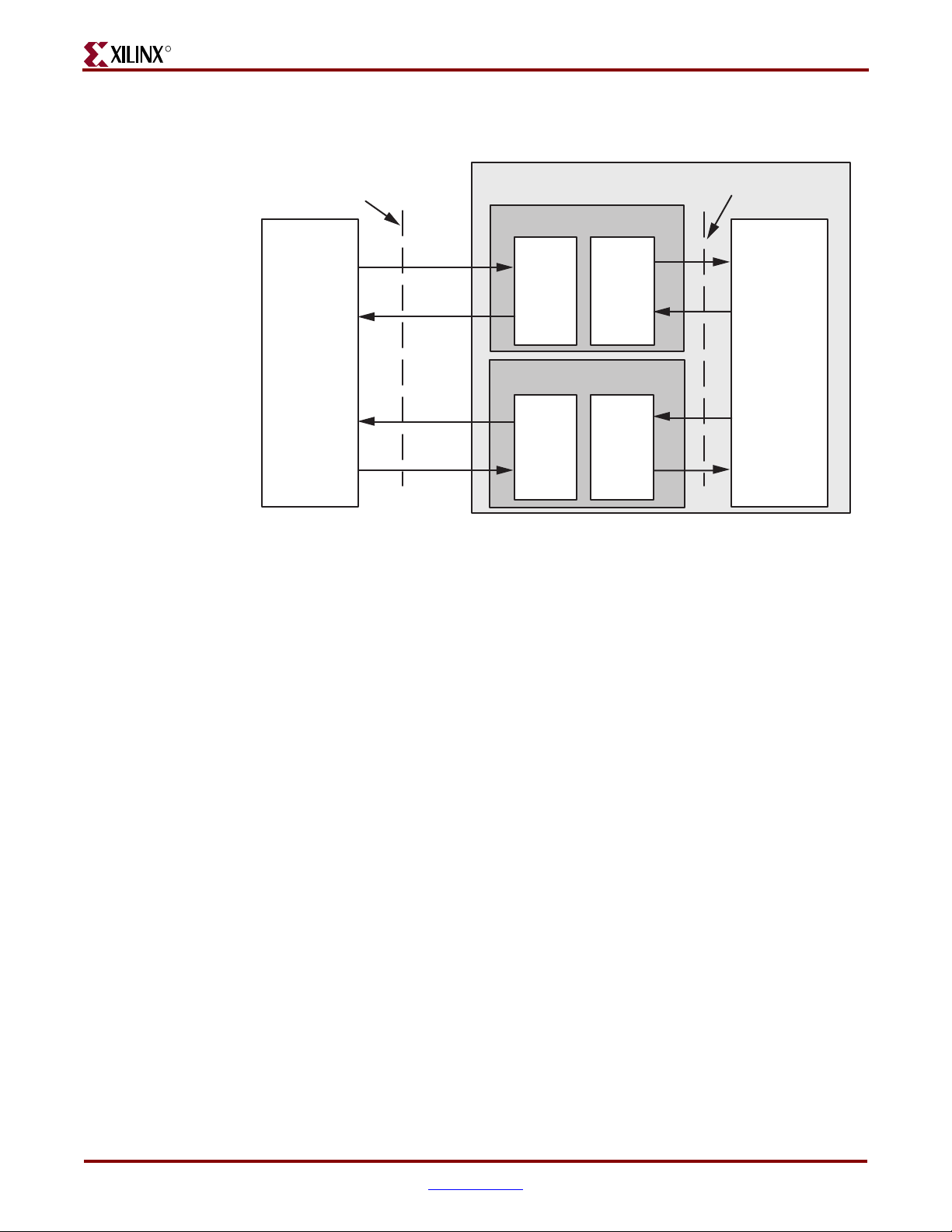
Figure 2-1 illustrates the interfaces of the SPI-4.2 Lite core and shows it in a typical link-
layer application.
In the link layer example, the SPI-4.2 interface connects an external physical-layer device to
a link-layer implemented in a Virtex™-4 FPGA. The user logic reads data from the Sink
core and writes data into the Source core. A standard FIFO interface is provided for this
SPI-4.2 Lite v4.3 User Guide www.xilinx.com 17
UG181 June 27, 2008
Page 18
R
Chapter 2: Core Architecture
data access and facilitates integration within a system. Dedicated signals are used to
configure the Sink and Source cores in circuit and monitor a suite of status registers.
Sink Core
SPI-4.2
Interface
SPI-4.2 Lite
PHY Layer Device
(Xilinx FPGA
or
ASSP)
Figure 2-1: SPI-4.2 Lite Core in a Typical Link Layer Application
Rx Data Path
Rx Status Path
Tx Data Path
Tx Status Path
Virtex-4 or Spartan-3 Device
SPI-4.2 Lite Sink Core
SPI-4.2
Sink
Interface
SPI-4.2 Lite Source Core
SPI-4.2
Source
Interface
User
Sink
Interface
User
Source
Interface
User
Interface
User’s Logic
(Link Layer
Processor)
The Sink core receives data from the SPI-4.2 interface. It takes the 16-bit interface and maps
it to a 32-bit or 64-bit interface enabling the internal logic to run at a half (for 32-bit) or an
quarter (for 64-bit) of the line rate. The user data and the corresponding control signals are
accessed with a standard FIFO interface. The FIFO read and write operations are
performed in independent clock domains.
The Sink core implements the following features:
• Supports 32-bit or 64-bit user data width
• Dedicated output signal indicating loss of valid RDClk
• Provides a FIFO reset signal for clearing contents of the data pipe during operation
• Provides support for forcing the insertion of DIP-2 errors for system testing
• Regional clocking option (for Virtex-4 and Virtex-5 devices only, saves global clocking
• Provides both embedded and user clocking options
For more information on core features, see Chapter 4, “Designing with the Core.”
Source Core
The Source core transmits data on the SPI-4.2 interface. Payload data written into the core
as 32-bit or 64-bit words (two or four 16-bit SPI-4.2 Lite words, respectively) are mapped
onto the 16-bit SPI-4.2 interface. While packet data written into the core may not be 32-bit
or 64-bit aligned, the core optimally maps the data to 16-bit words such that no filler idle
cycles are inserted. The data along with the control signals are written into the core via a
resources)
18 www.xilinx.com SPI-4.2 Lite v4.3 User Guide
UG181 June 27, 2008
Page 19

Sink Core Interfaces
standard FIFO interface, and the FIFO read and write operations are performed in
independent clock domains.
The Source core implements the following features:
• Supports 32-bit or 64-bit user data width.
• Optionally transmits only complete data bursts.
• Provides both master and slave clocking to facilitate multiple core implementations.
• Enables addressable or transparent access to SPI-4.2 flow control data.
• Provides a FIFO reset signal for clearing contents of the data pipe during operation.
• Provides support for forcing the insertion of DIP-4 errors for system testing.
For more information on core features, see Chapter 4, “Designing with the Core.”
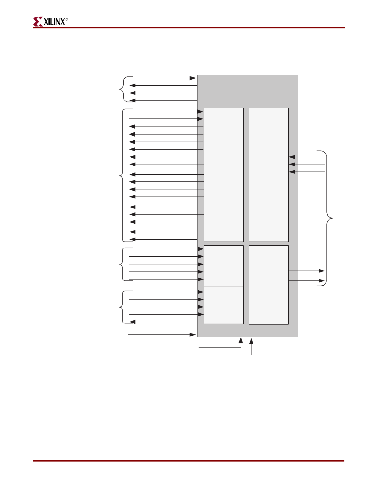
Sink Core Interfaces
The Sink core has five functional modules:
• Sink Data FIFO
• Sink Data Receive
• Sink Status Registers
• Sink Calendar
• Sink Status Transmit
R
The Sink core has the following interfaces:
• Sink SPI-4.2 Interface
• Sink User Interface
♦ Sink Control and Status Interface
♦ Sink FIFO Interface
♦ Sink Status and Flow Control Interface
- Calendar Control Interface
- Status FIFO Interface
♦ Sink Configuration Interface
♦ Sink Clocking Interface
SPI-4.2 Lite v4.3 User Guide www.xilinx.com 19
UG181 June 27, 2008
Page 20
R
4
a
Chapter 2: Core Architecture
The functional modules and signals which comprise the different interfaces are shown in
Figure 2-2 and defined in tables in the following sections.
Control
and
Status
nterface
FIFO
nterface
FIFO
Status
nterface
alendar
Control
nterface
SnkEn
SnkOof
SnkBusErr
SnkTrainValid
SnkFFClk
SnkFFRdEn_n
SnkFFAddr[7:0]
SnkFFData[63:0] or [31:0]
SnkFFMod[2:0] or [1:0]
SnkFFSOP
SnkFFEOP
SnkFFErr
SnkFFPayloadErr
SnkFFDIP4Err
SnkFFPa
yloadDIP4
SnkFFBurstErr
SnkFFAlmostEmpty_n
SnkFFEmpty_n
SnkFFValid
SnkAlmostFull_n
SnkOverflow_n
SnkStatClk
SnkStatAddr[3:0]
SnkStat[31:0]
SnkStatWrEn_n
SnkStatMask[15:0]
SnkCalClk
SnkCalWrEn_n
SnkCalAddr[8:0]
SnkCalData[7:0]
SnkCalDataOut[7:0]
SPI-4.2 Lite Sink Core
Sink Data
FIFO
Sink Status
Registers
Sink
Calendar
Sink Data
Receive
Sink Status
Transmit
RDClk
RDat[15:0]
RCtl
SPI-
Sin
Interf
RSClk
RStat[1:0]
Static Configuration Signals
Reset_n
SnkFifoReset_n
Figure 2-2: Sink Core Block Diagram
20 www.xilinx.com SPI-4.2 Lite v4.3 User Guide
UG181 June 27, 2008
Page 21

Sink Core Interfaces
Sink SPI-4.2 Interface
R
The SPI-4.2 interface uses LVDS I/O buffers to receive 16-bit data words. The 16-bit data
words received on the SPI-4.2 interface are combined into 32-bit or 64-bit data words by the
SPI-4.2 Lite core, which allows the user interface to run at a half (32-bit interface) or quarter
(64-bit interface) of the data rate. For example, for a 200 Mbps data rate and a 32-bit
interface, you can read data from the Sink core at 100 MHz, and if a 64-bit interface is used,
you can read data from the Sink core at 50 MHz and maintain the same data rate.
The resulting data words are written into an asynchronous FIFO. The received 16-bit
control words are stored out of band in the FIFO, along with the corresponding data word.
The received control words that are not idle or training words can contain the information
listed below:
• Start or continuation of the following packet
• Link address of the following packet
• End of the preceding packet
• Number of valid bytes in the last word of the preceding packet
• Error conditions in the preceding packet
In addition to receiving 16-bit data words, the SPI-4.2 interface also sends flow control data
at 1/4 rate (or 1/8 rate) of its data interface. The 32-bit status (2-bit status for each channel)
from the user interface is processed and formatted by the SPI-4.2 Lite core to be transmitted
on RStat. Tab le 2 -1 defines the Sink SPI-4.2 interface signals.
Table 2-1: Sink SPI-4.2 Interface Signals
Name Direction
RDClk_P
RDClk_N
RDat_P[15:0]
RDat_N[15:0]
RCtl_P
Input n/a SPI-4.2 Receive Data Clock (LVDS): Source synchronous clock received with
Input RDClk SPI-4.2 Receive Data Bus (LVDS): The 16-bit data bus used to receive SPI-4.2
Input RDClk SPI-4.2 Receive Control (LVDS): Signal that indicates whether data or control
RCtl_N
RSClk Output n/a SPI-4.2 Receive Status Clock: Source synchronous clock transmitted with
RStat[1:0] Output RSClk SPI-4.2 Receive FIFO Status: FlFO Status Channel flow control interface. You
Clock
Domain
Description
RDat and RCtl. The rising and falling edges of this clock (DDR) are used to
clock RDat and RCtl.
data and control information.
information is present on the RDat bus. When
present on RDat. When RCtl is asserted, control information is present on
RDat.
RStat at 1/2 or 1/4 rate of the RDClk. The rate of the status clock is controlled
by the static configuration signal RSClkDiv. You can select this signal to be
transmitted as LVTTL or LVDS.
can select this bus to be transmitted as LVTTL or LVDS.
RCtl is deasserted, data is
SPI-4.2 Lite v4.3 User Guide www.xilinx.com 21
UG181 June 27, 2008
Page 22

R
Sink User Interface
The Sink User Interface includes all signals other than those on the SPI-4.2 Interface. The
high-performance logic on the Sink back-end enables the user interface to run at higher
frequencies than the SPI-4.2 Interface. This is sometimes required if a large percentage of
the traffic consists of small packets.
The User Interface is subdivided into five smaller interfaces. Each of these interfaces are
presented in detail below:
• Control and Status Interface: The signals of this interface apply to the operation of
the Sink core.
• FIFO Interface: The signals of this interface allow you to access data received on the
SPI-4.2 Interface.
• Status and Flow Control Interface: The signals of this interface send flow control
information on the SPI-4.2 Interface.
• Static Configuration Interface: The signals of this interface allow you to configure the
core.
• Clocking Interface: The signals of this interface report the status of the clocks and
include the general purpose clocks.
Chapter 2: Core Architecture
Sink Control and Status Interface
The Sink core control and status signals either control the operation of the entire Sink core
or provide status information that is not associated with a particular channel (port) or
packet. Tab le 2 -2 defines the Sink control and status signals.
Table 2-2: Sink Control and Status Signals
Name Direction
Reset_n Input n/a Reset: Active Low signal that asynchronously initializes internal flip-flops,
SnkFifoReset_n Input SnkFFClk Sink FIFO Reset: Active low signal enables you to reset the Sink FIFO and
SnkEn Input SnkStatClk Sink Enable: Active high signal that enables the Sink core. When SnkEn is
Clock
Domain
Description
registers, and counters. When Reset_n is asserted, the Sink core will go out
of frame and the entire data path is cleared (including the FIFO). The Sink
core will also assert SnkOof, and deassert SnkBusErr and SnkTrainValid.
When Reset_n is asserted, the Sink core will transmit framing "11" on RStat
and continue to drive RSClk.
Following the deassertion of Reset_n, the sink calendar should be
programmed if the calendar is initialized in-circuit.
the associated data path logic. This enables the FIFO to be cleared while
remaining in frame.
Coming out of SnkFifoReset_n, the Sink core will discard all data on the SPI-
4.2 interface until a valid SOP control word is received.
deasserted, the Sink core will go out of frame and will not store any
additional data in the FIFO. The current contents of the FIFO remain intact.
The Sink core will also assert SnkOof, and deassert SnkBusErr and
SnkTrainValid. When SnkEn is deasserted, the Sink core will transmit
framing "11" on RStat and continue to drive RSClk.
22 www.xilinx.com SPI-4.2 Lite v4.3 User Guide
UG181 June 27, 2008
Page 23

Sink Core Interfaces
Table 2-2: Sink Control and Status Signals (Continued)
R
Name Direction
SnkOof Output SnkFFClk Sink Out-of-Frame: Active high signal that indicates that the SPI-4.2 Lite
SnkBusErr Output SnkFFClk Sink Bus Error: Active high signal that indicates SPI-4.2 protocol violations
SnkBusErrStat[7:0] Output SnkFFClk Sink Bus Error Status: Each bit of this bus corresponds to a specific Sink Bus
Clock
Domain
Description
Sink block is not in frame. This signal is asserted when SnkEn is deasserted
or the Sink block loses synchronization with the data received on the SPI-4.2
Interface. This signal is deasserted once the Sink block reacquires
synchronization with the received SPI-4.2 data.
or bus errors that are not associated with a particular packet. Information on
the specific error condition that caused the SnkBusErr assertion is provided
on SnkBusErrStat
Error condition and is asserted concurrently with SnkBusErr. The error
conditions detected are reported as follows:
SnkBusErrStat [0]: Minimum SOP spacing violation
SnkBusErrStat [1]: Control word with EOP not preceded by a data word
SnkBusErrStat [2]: Payload control word not followed by a data word
SnkBusErrStat [3]: DIP4 error received during training or on idles
SnkBusErrStat [4]: Reserved control words received
SnkBusErrStat [5]: Non-zero address bits on control words received (except
on payload and training control words)
SnkBusErrStat [6:7]: Reserved bits (tied low)
SnkTrainValid Output SnkFFClk Sink Training Valid: Active high signal that indicates that a valid training
pattern has been received. This signal is asserted for the duration of the
training pattern (20 SPI-4.2 bus clock cycles or 5 RDClk0_GP clock cycles), if
the training pattern received is successfully decoded.
Sink FIFO Interface
The Sink FIFO Interface signals allow you to access the data (received on the SPI-4.2
Interface) that is stored in the FIFO. The signals on this interface is defined in Ta bl e 2- 3.
Table 2-3: Sink FIFO Signals
Name
SnkFFClk Input Sink FIFO Clock: All Sink FIFO Interface signals are synchronous to the rising edge of
SnkFFRdEn_n Input Sink FIFO Read-Enable: When detected low at the rising edge of SnkFFClk, data and
SnkFFAddr[7:0] Output Sink FIFO Channel Address: Channel number associated with the data on SnkFFData.
SnkFFData[31:0]
or
SnkFFData[63:0]
SnkFFMod[1:0]
or
SnkFFMod[2:0]
Direction
this clock.
status information is available from the FIFO on the next rising edge of SnkFFClk.
Output Sink FIFO Data Out: The Sink FIFO data bus. Bit 0 is the LSB.
The core can be configured to have a 32- or 64-bit Interface. The 64-bit interface enables
running at half the clock rate required for a 32-bit interface.
Output Sink FIFO Modulo: This signal indicates which bytes on the SnkFFData bus are valid
when the SnkFFEOP signal is asserted.
SnkFFMod[1:0] is used with a 32-bit interface.
SnkFFMod[2:0] is used with a 64-bit interface.
Description
SPI-4.2 Lite v4.3 User Guide www.xilinx.com 23
UG181 June 27, 2008
Page 24

R
Table 2-3: Sink FIFO Signals (Continued)
Chapter 2: Core Architecture
Name
Direction
Description
SnkFFSOP Output Sink FIFO Start of Packet: When asserted (active high), this signal indicates the start of
a packet is being read out of the Sink FIFO.
SnkFFEOP Output Sink FIFO End of Packet: When asserted (active high), this signal indicates that the end
of a packet is being read out of the Sink FIFO.
SnkFFErr Output Sink FIFO Error: When asserted (active high), this signal indicates that the current
packet is terminated with an EOP abort condition. This signal is only asserted when
SnkFFEOP is asserted.
SnkFFEmpty_n Output Sink FIFO Empty: When asserted (active low), this signal indicates that the Sink FIFO
is empty. No data can be read until this signal is deasserted. This signal is asserted with
the last data word read out of the FIFO.
SnkFFAlmostEmpty_n Output Sink FIFO Almost Empty: When this signal is asserted (active low), it indicates that one
word remains in the FIFO, and you should deassert the read enable signal on the next
clock cycle. The user ’s read logic should evaluate the SnkFFEmpty_n signal to verify
that there is no data in the FIFO in case an additional word was simultaneously written
into the FIFO. An example of the behavior of this interface signal is provided with the
SPI-4.2 Lite core in the Design Example (see the pl4_lite_fifo_loopback_read.v/vhd file.)
SnkFFValid Output Sink FIFO Read Valid: When asserted (active high), this signal indicates that the
information on SnkFFData, SnkFFAddr, SnkFFSOP, SnkFFEOP, SnkFFBurstErr,
SnkFFMod, SnkFFErr, SnkFFDIP4Err, and SnkFFPayloadErr is valid.
SnkFFDIP4Err Output Sink FIFO DIP-4 Error: When asserted (active high), this signal indicates that a DIP-4
parity error was detected with the SPI-4.2 control word ending a packet or burst of data.
This signal is asserted at the end of that packet or burst of data.
SnkFFPayloadDIP4 Output Sink FIFO Payload DIP4 Error: When asserted (active high), this signal indicates that a
DIP-4 parity error was detected with the SPI-4.2 control word starting a packet or burst
of data. This signal is asserted at the end of that packet or burst of data.
SnkFFBurstErr Output Sink FIFO Burst Error: When asserted (active high), this signal indicates that the Sink
core has received data that was terminated on a non-credit boundary without an EOP.
SnkFFBurstErr may be used by the user’s logic to indicate missing EOPs, or incorrectly
terminated bursts. In this case the Sink core does not assert SnkFFEOP or SnkFFErr.
SnkFFPayloadErr Output Sink FIFO Payload Error: When asserted (active high), this signal indicates that the
received data was not preceded by a valid payload control word. Since it is not clear
what the packet Address and SOP should be, it is flagged as an error. This is asserted
with each data word coming out of the FIFO, and will remain asserted until a valid
payload control word is followed by data.
SnkAlmostFull_n Output Sink Almost Full: When asserted (active low), this signal indicates that the Sink core is
approaching full (as defined by the parameter SnkAFThresAssert), and that immediate
action should be taken to prevent overflow.
SnkOverflow_n Output Sink Overflow: When asserted (active low), this signal indicates that the Sink core has
overflowed and is in an error condition. Data will be lost if SnkOverflow_n is asserted,
since no data is written into the FIFO when the overflow signal is asserted.
24 www.xilinx.com SPI-4.2 Lite v4.3 User Guide
UG181 June 27, 2008
Page 25

Sink Core Interfaces
Sink Status and Flow Control Interface (Calendar Control and Status FIFO)
The Sink Status and Flow Control interface enables you to send flow control data on the
SPI-4.2 Interface. The status information is sent based on the channel order and channel
frequency defined in the programmable calendar. Ta bl e 2- 4 and Ta bl e 2- 5 define the
calendar interface and status FIFO interface signals.
Table 2-4: Sink Calendar Control Signals
R
Name Direction
SnkCalClk Input n/a Sink Calendar Clock: All Sink calendar signals are synchronous to
SnkCalWrEn_n Input SnkCalClk Sink Calendar Write Enable: When this signal is asserted (active
SnkCalAddr[8:0] Input SnkCalClk Sink Calendar Address: When SnkCalWrEn_n is asserted, this bus
SnkCalData[7:0] Input SnkCalClk Sink Calendar Data: This bus contains the channel number to write
SnkCalDataOut[7:0] Output SnkCalClk Sink Calendar Data Output: This bus contains the channel number
Clock
Domain
Description
this clock.
low), the Sink Calendar is written with the data on the SnkCalData
bus on the rising edge of SnkCalClk. When the signal is deasserted,
the Sink Calendar data can be read on SnkCalDataOut.
indicates the calendar address to which the data on SnkCalData is
written. When SnkCalWrEn_n is deasserted, this bus indicates the
calendar address from which the channel number on SnkCalDataOut
is driven.
into the calendar buffer when SnkCalWrEn_n is enabled. The channel
numbers written into the calendar indicate the order that status is
sent on RStat.
that is read from the calendar buffer when SnkCalWrEn_n is disabled.
The channel numbers read from the calendar indicate the order that
status is sent on RStat.
Table 2-5: Sink Status FIFO Signals
Name Direction
SnkStatClk Input n/s Sink Status Clock: All Sink Status write signals are synchronous to
SnkStat[31:0] Input SnkStatClk Sink Status Bus: This 32-bit bus is used to write status information
SnkDIP2ErrRequest Input SnkStatClk Sink DIP2 Error Request: This is an active high signal that requests
SPI-4.2 Lite v4.3 User Guide www.xilinx.com 25
UG181 June 27, 2008
Clock
Domain
Description
this clock.
into the Status FIFO. You can write the status for 16 channels each
clock cycle.
The 16-channel status that are accessed simultaneously are grouped
in the following manner: channels 15 to 0, channels 31 to 16, channels
47 to 32, . . . , channels 255 to 239.
an incorrect DIP-2 to be sent out of the RStat bus. When this signal is
asserted, Sink Status FIFO responds by inverting the next DIP2 value
that it transmits.
Page 26

R
Table 2-5: Sink Status FIFO Signals (Continued)
Chapter 2: Core Architecture
Name Direction
SnkStatAddr[3:0] Input SnkStatClk Sink Status Address bus: The Sink Status Address determines the
SnkStatWr_n Input SnkStatClk Sink Status Write: The Sink Status Write (active low) qualifies the
SnkStatMask[15:0] Input SnkStatClk Sink Status Mask Bus: The Sink Status Mask determines if the 2-bit
Clock
Domain
Description
group of 16-channel status that SnkStat will be updating.
Bank 0: SnkStatAddr=0, channels 15 to 0
Bank 1: SnkStatAddr=1, channels 31 to 16
Bank 2: SnkStatAddr=2, channels 47 to 32
. . .
Bank 15: SnkStatAddr=15, channels 255 to 239
SnkStatMask signal. When SnkStatWr_n is asserted (active low),
status for the different channels is updated. When SnkStatWr_n is
deasserted (active high), SnkStat input is ignored.
status among the corresponding group of 16 channels of status on
SnkStat (being addressed by SnkStatAddr) will be updated when
SnkStatWr_n is asserted (active low):
SnkStatMask[x] = 1, status for channel (x+(SnkStatAddr*16)) will be
updated.
SnkStatMask[y] = 0, status for channel (y+(SnkStatAddr*16)) will not
be updated.
For example, if SnkStatMask[15] = 1 and SnkStatAddr = 1, then
SnkStat[31:30] = 00 will overwrite the current status on channel 31. If
SnkStatMask is all zeros, none of the sixteen 2-bit status values will
be updated. If SnkStatMask is all ones, all sixteen of the 2-bit status
values will be updated.
Sink Static Configuration Interface
These signals are inputs to the core that are statically driven by setting them to a constant
value in the top-level wrapper file. The SPI-4.2 Lite release includes a wrapper file that has
the static configuration signals connected to the values selected in the CORE Generator
GUI. Customization of these signals can be done using the GUI.
Two of the Sink Static Configuration signals can be changed in circuit. There are static
registers for
To change these parameters while the core is operational,
If you sets the configuration signal to an illegal number, the core is automatically set to the
minimum value. Ta bl e 2 -6 defines the Sink Static Configuration signals.
SnkCalendar_M and SnkCalendar_Len that are synchronous to SnkStatClk.
SnkEn must first be deasserted.
26 www.xilinx.com SPI-4.2 Lite v4.3 User Guide
UG181 June 27, 2008
Page 27

Sink Core Interfaces
Table 2-6: Sink Static Configuration Signals
Name Direction Range Description
R
NumDip4Errors[3:0] Static
Input
NumTrainSequences[3:0] Static
Input
1-15
Value of 0 is set to 1
1-15
Value of 0 is set to 1
SnkCalendar_M[7:0] Input 0-255
(effective range 1-256)
SnkCalendar_Len[8:0] Input 0-511
(effective range 1-512)
Number of DIP-4 Errors: The Sink Interface will go
out-of-frame (assert SnkOof) and stop accepting data
from the SPI-4.2 bus after receiving NumDip4Errors
consecutive DIP-4 errors.
Number of Complete Training Sequences: A
complete training pattern consists of 10 training
control words and 10 training data words. The Sink
interface requires NumTrainSequences consecutive
training patterns before going in frame (deasserting
SnkOof) and accepting data from the SPI-4.2 bus.
Sink Calendar Period: The SnkCalendar_M parameter
sets the number of repetitions of the calendar sequence
before the DIP-2 parity and framing words are
inserted.
The core implements this parameter as a static register
synchronous to SnkStatClk, and it can be updated in
circuit by first deasserting SnkEn.
Note that the Sink Calendar Period equals
SnkCalendar_M + 1. For example, if
SnkCalendar_M=22, the Sink Calendar Period will be
equal to 23.
Sink Calendar Length: The SnkCalendar_Len
parameter sets the length of the calendar sequence.
The core implements this parameter as a static register
synchronous to SnkStatClk, and it can be updated in
circuit by first deasserting SnkEn.
Note that the Sink Calendar Length equals
SnkCalendar_Len + 1. For example, if
SnkCalendar_Len=15, the Sink Calendar Length will
be equal to 16.
SnkAFThresAssert[8:0] Static
Input
1–508
Values less than1 are
set to 1.
Values greater than
508 are set to 508.
Sink Almost Full Threshold Assert: The
SnkAFThresAssert parameter defines the minimum
number of empty FIFO locations that exist when
SnkAlmostFull_n is asserted. Note that the assert
threshold must be less than or equal to the negate
threshold (SnkAFThresNegate).
When SnkAlmostFull_n is asserted, the core initiates
the flow control mechanism selected by the parameter
FifoAFMode. The FifoAFMode defines when the
interface stops sending valid FIFO status levels and
begins sending flow control information on RStat. This
indicates to the transmitting device that the core is
almost full and additional data cannot be sent.
SPI-4.2 Lite v4.3 User Guide www.xilinx.com 27
UG181 June 27, 2008
Page 28

R
Table 2-6: Sink Static Configuration Signals (Continued)
Name Direction Range Description
Chapter 2: Core Architecture
SnkAFThresNegate[8:0] Static
Input
RSClkDiv Static
Input
RSClkPhase Static
Input
FifoAFMode[1:0] Static
Input
SnkAFThresAssert to
508
Values less than
SnkAFThresAssert are
set to
SnkAFThresAsset.
Values greater than
508 are set to 508.
Sink Almost Full Threshold Negate: The
SnkAFThresNegate parameter defines the minimum
number of empty FIFO locations that exist when
SnkAlmostFull_n is deasserted. Note that the negate
threshold must be greater or equal to the assert
threshold (SnkAFThresAssert).
When SnkAlmostFull_n is deasserted, the core stops
sending flow control (deasserts SnkAlmostFull_n) and
resumes transmission of valid FIFO status levels. This
indicates to the transmitting device that additional
data can be sent.
n/a Sink Status Clock Divide: This static input is used to
determine if the RSClk is 1/4 of the data rate, which is
compliant with the OIF specification, or 1/8 of the data
rate, which is required by some PHY ASSPs:
0: RSClkDiv = 1/4 rate (default value)
1: RSClkDiv = 1/8 rate
n/a Sink Status Clock Phase: This static input determines
whether the FIFO Status Channel data (RStat[1:0])
changes on the rising edge of RSClk or the falling edge
of RSClk:
0: RSClkPhase = rising edge of RSClk (default value)
1: RSClkPhase = falling edge of RSClk
n/a Sink Almost Full Mode: Selects the mode of operation
for the Sink interface when the Sink core reaches the
Almost Full threshold (SnkAFThresAssert).
If FifoAFMode is set to “00,” the Sink interface goes
out-of-frame when the core is almost full, and the Sink
Status logic sends the framing sequence “11” until Sink
core is not almost full.
If FifoAFMode is set to “01,” the Sink interface remains
in frame (SnkOof deasserted), and the Sink Status logic
sends satisfied “10” on all channels until
SnkAlmostFull_n is deasserted.
If FifoAFMode is set to “10” or “11,” the Sink interface
will remain in frame (SnkOof deasserted), and the Sink
Status logic continues to drive out the user’s status
information (i.e., continues in normal operation). In
this case, you should take immediate action to prevent
overflow and loss of data.
28 www.xilinx.com SPI-4.2 Lite v4.3 User Guide
UG181 June 27, 2008
Page 29
Sink Core Interfaces
Sink Clocking Interface
R
The Sink core supports two clocking implementations: embedded clocking and user
clocking. The embedded clocking configuration provides a complete solution with the
clock circuitry embedded within the Sink core. The user clocking configuration allows the
clocking scheme to be implemented external to the Sink core.
A list of the Sink clocks for embedded clocking and their description is provided in
Tab le 2 -7. Ta bl e 2-8 defines the DCM reset and clock status signals, and Tab le 2 -9 defines
the user clocking signals. The minimum frequency for all clocks is dependent on the
minimum frequency of the DCM.
Table 2-7: Sink Core Clocks: Embedded Clocking
Clock Pins Direction Description Max. Frequency
RDClk0_GP Output
(User Interface)
RDClk180_GP Output
(User Interface)
RDClk0 General Purpose:
This clock is the full Rate
Receive Data Clock. It is
used for clocking the
internal logic of the core and
is routed to the User
Interface for use by the
user’s logic.
RDClk180 General
Purpose: This clock is the
inverted equivalent of
RDClk0_GP. It is used for
clocking the internal logic of
the core and is routed to the
User Interface for use by the
user’s logic.
Table 2-8: Sink Core Clocks: Status Signals
Name Direction
Clock
Domain
Virtex-5: 275 MHz
Virtex-4: 190 MHz
Virtex-II Pro: 160 MHz
Virtex-II: 160 MHz
Spartan-3: 115 MHz
Spartan-3E: 90 MHz
Spartan-3A/3AN/3A DSP:
105 MHz
Virtex-5: 275 MHz
Virtex-4: 190 MHz
Virtex-II Pro: 160 MHz
Virtex-II: 160 MHz
Spartan-3: 115 MHz
Spartan-3E: 90 MHz
Spartan-3A/3AN/3A DSP:
105 MHz
Description
DCMReset_RDClk Input N/A Reset of RDClk’s DCM
Locked_RDClk Output N/A Locked status of RDClk’s DCM
DCMLost_RDClk Output N/A Indicates RDClk input has stopped (status bit
one of RDClk DCM)
SnkClksRdy Output N/A Indicates all Sink core clocks are ready for use
SPI-4.2 Lite v4.3 User Guide www.xilinx.com 29
UG181 June 27, 2008
Page 30

R
Chapter 2: Core Architecture
Table 2-9: Sink Core Clocks: User Clocking
Clock Pins Direction Description Max. Frequency
RDClk0_USER Input
RDClk180_USERInput
Source Core Interfaces
The Source core includes five functional modules:
• Source Data FIFO
• Source Data Transmit
• Source Status Registers
• Source Calendar
• Source Status Receive
(User Interface)
(User Interface)
RDClk0_USER: This clock
is used for clocking the
internal logic of the core.
RDClk180_USER: This
clock is the inverted
equivalent of
RDClk0_USER. It is used
for clocking the internal
logic of the core.
Virtex-5: 275 MHz
Virtex-4: 190 MHz
Virtex-II Pro: 160 MHz
Virtex-II: 160 MHz
Spartan-3: 115 MHz
Spartan-3E: 90 MHz
Spartan-3A/3AN/3A DSP:
105 MHz
Virtex-5: 275 MHz
Virtex-4: 190 MHz
Virtex-II Pro: 160 MHz
Virtex-II: 160 MHz
Spartan-3: 115 MHz
Spartan-3E: 90 MHz
Spartan-3A/3AN/3A DSP:
105 MHz
The Source core is comprised of the following interfaces:
• Source SPI-4.2 Interface
• Source User Interface
♦ Source Control and Status Interface
♦ Source FIFO Interface
♦ Source Status and Flow Control Interface
- Calendar Control Interface
- Status FIFO Interface
♦ Source Configuration Signals Interface
♦ Source Clocking Interface
30 www.xilinx.com SPI-4.2 Lite v4.3 User Guide
UG181 June 27, 2008
Page 31

Source Core Interfaces
Figure 2-3 illustrates the functional modules and signals in each interface—all signals are
defined in sections following this illustration.
SysClk
Control
and Status
Interface
FIFO
Interface
FIFO
Status
Interface
Calendar
Control
Interface
SrcEn
SrcOof
SrcDIP2Err
SrcPatternErr
IdleRequest
TrainingRequest
SrcFFClk
SrcFFWrEn_n
SrcFFAddr[7:0]
SrcFFData[63:0] or [31:0]
SrcFFMod[2:0] or [1:0]
SrcFFSOP
SrcFFEOP
SrcFFErr
SrcFFOverflow_n
SrcFFAlmostFull_n
SrcStatClk
SrcStatAddr[3:0]
SrcStat[31:0]
SrcStatCh[7:0]
SrcStatChValid
SrcCalClk
SrcCalWrEn_n
SrcCalAddr[8:0]
SrcCalData[7:0]
SrcCalDataOut[7:0]
SPI-4.2 Lite Source Core
Source Data
FIFO
Source Status
Registers
Source
Calendar
TDClk
TDat[15:0]
TCtl
Source Data
Transmit
SPI4.2
Source
Interface
TSClk
TStat[1:0]
Source Status
Receive
R
Static Configuration Signals
Reset_n
SrcFifoReset_n
SrcTriStateEn
Figure 2-3: Source Core Block Diagram and I/O Interface Signals
Source SPI-4.2 Interface
The SPI-4.2 interface uses LVDS I/O buffers to transmit 16-bit data words. The data words
received on the User Interface and the out-of-band control words are multiplexed onto the
SPI-4.2 Lite 16-bit databus. The source core supports a 32-bit and 64-bit user interface,
which allows it to run at a half (32-bit interface) or quarter (64-bit interface) of the data rate.
For example, for a 200 Mbps SPI-4.2 data rate and a 32-bit interface, you can write data into
the Source core at 100 MHz. If a 64-bit interface is used, you can write data into the Source
core at 50 MHz and maintain the same data rate.
SPI-4.2 Lite v4.3 User Guide www.xilinx.com 31
UG181 June 27, 2008
Page 32

R
Chapter 2: Core Architecture
In addition to transmitting 16-bit data words, the SPI-4.2 interface also receives flow
control data at 1/4 rate of its data interface. The 2-bit status received can be presented to
you in 2 interfaces: transparent and addressable.
Tab le 2 -10 defines the Source SPI-4.2 interface signals.
Table 2-10: Source SPI-4.2 Interface Signals
Name Direction
TDClk_P
TDClk_N
TDat_P[15:0]
TDat_N[15:0]
TCtl_P
TCtl_N
TSClk
TStat[1:0] Input
Output n/a SPI-4.2 Transmit Data Clock (LVDS): Source
Output TDClk SPI-4.2 Transmit Data Bus (LVDS): The 16-bit data
Output TDClk SPI-4.2 Transmit Control (LVDS): SPI-4.2 Interface
Input n/a SPI-4.2 Transmit Status Clock: Source
Clock
Domain
TSClk
Description
synchronous clock transmitted with TDat. The
rising and falling edges of this clock (DDR) are
used to clock TDat and TCtl.
bus is used to transmit SPI-4.2 data and control
information.
signal that defines whether data or control
information is present on the TDat bus. When TCtl
is Low, data is present on TDat. When TCtl is High,
control information is present on TDat.
synchronous clock that is received by the Source
core with TStat at 1/4 rate (or 1/8 rate) of TDClk.
You can select this signal to be transmitted as
LVTTL o r LVD S .
SPI-4.2 Transmit FIFO Status: FlFO-StatusChannel flow control interface. You can select this
bus to be transmitted as LVTTL or LVDS.
Source User Interface
The Source User Interface includes all signals other than those on the SPI-4.2 interface. The
high performance logic on the Source back-end enables the user interface to run at higher
frequencies than the SPI-4.2 interface. This is sometimes required if a large percentage of
the traffic consists of small packets.
The Source User Interface is subdivided into 5 smaller interfaces. Each of these signal types
are presented in detail below:
• Control and Status Interface. The signals of this interface apply to the operation of
the Sink core.
• FIFO Interface. The signals of this interface allow you to access data received on the
SPI-4.2 Interface.
• Status and Flow Control Interface. The signals of this interface send flow control
information on the SPI-4.2 Interface.
• Static Configuration Interface.The signals of this interface allow you to configure the
core.
• Clocking Interface. The signals of this interface report the status of the clocks and
include the general purpose clocks.
32 www.xilinx.com SPI-4.2 Lite v4.3 User Guide
UG181 June 27, 2008
Page 33

Source Core Interfaces
Source Control and Status Interface
The Source Control and Status signals either control the operation of the entire Source core
or provide status information that is not associated with a particular channel (port) or
packet. Tab le 2 -11 defines the source control and status signals.
Table 2-11: Source Control and Status Signals
R
Name Direction
Reset_n Input n/a Reset_n: This active low, asynchronous control signal enables you to restart the
SrcFifoReset_n Input SrcFFClk SrcFifoReset_n: This active low control signal enables you to reset the Source
SrcEn Input SrcStatClk Source Enable: Active high signal that enables the Source core. When SrcEn is
SrcOof Output SrcFFClk Source Out-of-Frame: When this signal is asserted (active high), it indicates
Clock
Domain
Description
entire Source core. This means that the core will go out-of-frame. While Reset_n
is asserted, the Source core transmits idles cycles on TDat. Coming out of
Reset_n, the Source core transmits training patterns.
Following the release of Reset_n, the Source Calendar should be programmed
if the calendar is to be initialized in-circuit.
FIFO and the associated data path logic. This enables the FIFO to be cleared
while remaining in frame.
Upon Source FIFO Reset, the Source core sends idle cycles until you writes data
into the FIFO.
deasserted, the Source core will not store or verify received status information.
The Source core will also assert SrcOof, and deassert SrcDIP2Err and
SrcPatternErr. When SrcEn is deasserted, the Source core will transmit training
patterns on TDat.
that the SPI-4.2 Lite Source core is not in frame. This signal is asserted when the
Source core has lost synchronization on the transmit FIFO status interface. This
is caused by the receipt of consecutive DIP-2 parity errors (determined by the
parameter NumDip2Errors), invalid received status frame sequence (of four
consecutive frame words "11"), or when SrcEn is deasserted.
This signal is deasserted once the Source core reacquires synchronization with
the SPI-4.2 transmit Status Channel. Synchronization occurs when consecutive
valid DIP2 words (determined by the Static Configuration signal
NumDip2Matches) are received and SrcEn is asserted.
SrcOofOverride Input SrcFFClk Source Out-of-Frame Override: When this signal is asserted, the source core
behaves like it is in frame and sends data on TDat, regardless of the status
received on TStat. This signal is used for system testing and debugging.
SrcDIP2Err Output SrcFFClk Source DIP-2 Parity Error: When this signal is asserted (active high), it
indicates that a DIP-2 parity error was detected on TStat. This signal is asserted
for one clock cycle each time a parity error is detected.
SrcStatFrameErr Output SrcFFClk Source Status Frame Error: When this signal is asserted (active high), it
indicates that a non “11” frame word was received after DIP2 on TStat. This
signal is asserted for one clock cycle each time an error frame word is detected.
SPI-4.2 Lite v4.3 User Guide www.xilinx.com 33
UG181 June 27, 2008
Page 34

R
Table 2-11: Source Control and Status Signals (Continued)
Chapter 2: Core Architecture
Name Direction
SrcPatternErr Output SrcFFClk Source Data Pattern Error: When this signal is asserted (active high), it
Clock
Domain
Description
indicates that the data pattern written into the Source FIFO is illegal. Illegal
patterns include the following:
• Burst of data terminating on a non-credit boundary (not a multiple
of 16 bytes) with no EOP
• Non-zero value on SrcFFMod when SrcFFEOP is deasserted
This signal is asserted for one clock cycle each time an illegal data pattern is
written into the Source FIFO.
IdleRequest Input SrcFFClk Idle Request: This is an active high signal that requests idle control words be
sent out of the Source SPI-4.2 interface. The Source core responds by sending
out idle control words at the next burst boundary. This signal overrides normal
SPI-4.2 data transfer requests, but it does not override training sequence
requests (TrainingRequest).
Activating the request for idle cycles does not affect the Source FIFO contents
or the user side operation.
TrainingRequest Input SrcFFClk Training Pattern Request: This is an active high signal that requests training
patterns be sent out of the Source SPI-4.2 interface. The Source core responds
by sending out training patterns at the next burst boundary. This signal
overrides idle requests (IdleRequest) and normal SPI-4.2 data transfers.
Activating the request for training cycles does not affect the Source FIFO
contents or the user side operation.
SrcTriStateEn Input SrcFFClk SrcTriStateEn: This is an active high control signal that enables you to tri-state
the IOB drivers for the following Source core outputs: TDClk, TDat[15:0], and
TCtl.
When SrcTriStateEn=0 the outputs are not tri-stated.
When SrcTriStateEn=1 the outputs are tri-stated.
Default setting for this signal is disabled (SrcTriStateEn=0.)
34 www.xilinx.com SPI-4.2 Lite v4.3 User Guide
UG181 June 27, 2008
Page 35

Source Core Interfaces
Source FIFO Interface
R
The Source FIFO Interface signals allow you to write data into the FIFO to be transmitted
on the SPI-4.2 Interface. Ta bl e 2- 12 defines the Source FIFO signals.
Table 2-12: S
SrcFFClk Input n/a Source FIFO Clock: All Source FIFO Interface signals are
SrcFFWrEn_n Input SrcFFClk Source FIFO Write-Enable: When asserted (active low) at the rising
SrcFFAddr[7:0] Input SrcFFClk Source FIFO Channel Address: Channel number associated with
SrcFFData[31:0]
or
SrcFFData[63:0]
SrcFFMod[1:0]
or
SrcFFMod[2:0]
SrcFFSOP Input SrcFFClk Source FIFO Start of Packet: When asserted (active high), this
ource FIFO Signals
Name Direction
Input SrcFFClk Source FIFO Data: The Source FIFO data bus. Bit 0 is the LSB. The
Input SrcFFClk Source FIFO Modulo: This signal indicates which bytes on the
Clock
Domain
Description
synchronous to the rising edge of this clock.
edge of SrcFFClk, data and packet information is written into the
FIFO.
the data on SrcFFData.
core can be configured to have a 32-bit or a 64-bit interface. The 64bit interface enables you to run at half the clock rate required for a
32-bit interface.
SrcFFData bus are valid when the SrcFFEOP or SrcFFErr signal is
asserted. When SrcFFEOP is deasserted, SrcFFMod should always
be zero.
SrcFFMod[1:0] is used with a 32-bit interface.
SrcFFMod[2:0] is used with a 64-bit interface.
signal indicates that the start of a packet is being written into the
Source FIFO.
SrcFFEOP Input SrcFFClk Source FIFO End of Packet: When asserted (active high), this signal
indicates that the end of a packet is being written into the Source
FIFO. May be concurrent with SrcFFSOP.
SrcFFErr Input SrcFFClk Source FIFO Error: When asserted (active high) simultaneously
with the SrcFFEOP flag, the current packet written into the FIFO
contains an error. This causes an EOP abort to be sent on the SPI-4.2
Interface.
SrcFFErr can be used in combination with SrcFFEOP to insert
erroneous DIP-4 values for testing purposes. When SrcFFErr is
asserted and SrcFFEOP is not asserted, the core inserts an EOP (1 or
2 bytes depending on the SrcFFMod value) with an erroneous DIP4 value. The erroneous DIP4 value is an inversion of the correctly
calculated value.
SrcFFAlmostFull_n Output SrcFFClk Source FIFO Almost Full: When asserted (active low), this signal
indicates that the FIFO is approaching full, and no more data
should be written.
SrcFFOverflow_n Output SrcFFClk Source FIFO Overflow: When asserted (active low), this signal
indicates that the FIFO has overflowed and is in an error condition.
No more data can be written until it is deasserted. SrcFFWrEn_n is
ignored if SrcFFOverflow_n is asserted.
SPI-4.2 Lite v4.3 User Guide www.xilinx.com 35
UG181 June 27, 2008
Page 36

R
Source Status and Flow Control Interface (Calendar Control and Status
FIFO)
The Source Status and Flow Control Interface enables you to receive flow control data from
the SPI-4.2 interface. The status information is received based on the channel order and
frequency defined in the programmable calendar. The Source Calendar Control signals are
defined in Tab le 2 -1 3. The Source Status FIFO Signals are defined in Tabl e 2- 14 . Tab le 2 -1 5
defines Source Static Configuration signals.
Table 2-13: Source Calendar Control Signals
Chapter 2: Core Architecture
Name Direction
SrcCalClk Input n/a Source Calendar Clock: All Source calendar signals are synchronous
SrcCalWrEn_n Input SrcCalClk Source Calendar Write Enable: When this signal is asserted (Active
SrcCalAddr[8:0] Input SrcCalClk Source Calendar Address: When SrcCalWrEn_n is asserted, this bus
SrcCalData[7:0] Input SrcCalClk Source Calendar Data: This bus contains the channel number to
SrcCalDataOut[7:0] Output SrcCalClk Source Calendar Data Output: This Source Calendar Data Output
Clock
Domain
Description
to this clock.
Low), the Source Calendar is loaded with the data on the SrcCalData
bus on the rising edge of SrcCalClk.
indicates the calendar address to which the data on SrcCalData is
written. When SrcCalWrEn_n is deasserted, this bus indicates the
calendar address from which the data on SrcCalDataOut is driven.
write into the calendar buffer when SrcCalWrEn_n is enabled. The
channel numbers written into the calendar indicate the order that
status is updated on the SrcStat bus.
bus contains the channel number that is read from the calendar buffer
when SrcCalWrEn_n is disabled. The channel numbers read from the
calendar indicates the order that status is updated on SrcStat bus.
Table 2-14: Source Status FIFO Signals
Name Direction
SrcStatClk
(Addressable I/F
Only)
SrcStat[31:0]
(Addressable I/F
Only)
SrcStat[1:0]
(Transparent I/F Only)
36 www.xilinx.com SPI-4.2 Lite v4.3 User Guide
Input n/a Source Status Clock: For the Addressable Interface, all Source Status
Output SrcStatClk
Clock
Domain
(Addressabl
e I/F only)
TSClk_GP
(Transparent
I/F only)
Description
read signals are synchronous to this clock.
For the Transparent Interface, this clock signal is not present. For this
interface, all signals are synchronous to TSClk_GP.
Source Status: For the Addressable Interface, the 32-bit Source Status
bus is the dedicated 16-channel interface. You can read the status for
16-channels each clock cycle. The 16-channel status that are accessed
simultaneously are grouped in the following manner: channel 15 to
0, channel 31 to 16, channel 47 to 32, ..., channel 255 to 240.
For the Transparent Interface, this Source Status bus is two bits wide
and represents the last status received.
UG181 June 27, 2008
Page 37

Source Core Interfaces
Table 2-14: Source Status FIFO Signals (Continued)
R
Name Direction
SrcStatAddr[3:0]
(Addressable I/F
Only)
SrcStatCh[7:0] Output TSClk_GP Source Status Channel: The Source Status Channel is an 8-bit bus
SrcStatChValid Output TSClk_GP Source Status Channel Valid: When asserted, Source Status Channel
Input SrcStatClk Source Status Address:
Clock
Domain
Description
For the Addressable Interface, the Source Status Address determines
which group of 16-channels gets its status driven onto SrcStat on the
following clock cycle. The address bus is associated with banks of
channels as follows:
Bank 0: SrcStatAddr=0 channel 15-0
Bank 1: SrcStatAddr=1, channel 31-16
Bank 2: SrcStatAddr=2, channel 47-32
...
Bank 15: SrcStatAddr=15 channel 255-240
For the Transparent Interface, this signal is not present.
containing the channel address that is being updated on the
SrcStatAddr bus in the current clock cycle.
Valid indicates that the value on SrcStatCh is valid. When the core is
processing DIP-2 or frame words, SrcStatChValid is deasserted. Note
that a transition of the SrcStatChValid from 0 to 1 indicates that the
core has started a new calendar sequence.
Source Static Configuration Interface
These signals are inputs to the core that are statically driven by setting them to a constant
value in the top-level wrapper file. The SPI-4.2 Lite release includes a wrapper file that has
the static configuration signals connected to the values selected in the CORE Generator
GUI. Customization of these signals is done using the GUI.
Three of the Source Static Configuration signals can be changed in-circuit. There are static
registers for
SrcCalendar_Len (synchronous to SrcStatClk.) To change these parameters while the
core is operational, you must first deassert
SrcBurstLen (synchronous to SrcFFClk), and SrcCalendar_M and
SrcEn.
SPI-4.2 Lite v4.3 User Guide www.xilinx.com 37
UG181 June 27, 2008
Page 38

R
Chapter 2: Core Architecture
Note that there are legal values for each of the signals. If the configuration signal is set to an
illegal number, the core automatically sets it to the minimum value. Ta bl e 2- 15 defines the
Source Static Configuration signals.
Table 2-15: Source Static Configuration Signals
Name Direction Range Description
SrcBurstMode Static Input 0 or 1 Source Burst Mode: When SrcBurstMode is set to zero,
the Source core transmits data in the FIFO if the data in
the FIFO is terminated by an EOP or if there is a
complete credit of data.
When SrcBurstMode is set to1, the Source core only
transmits data that is terminated by an EOP or when
there is data in the FIFO equal to the maximum burst
length defined by SrcBurstLen.
SrcBurstLen[5:0] Input 1-63
Values equal to 0 are set
to 1.
SrcAFThresAssert[8:0] Static Input If SrcBurstMode = 0
1 to 508
Values less than 1 are set
to 1.
Values greater than 508
are set to 508.
If SrcBurstMode = 1
SrcBurstLen to 508.
Values less than
SrcBurstLen are set to
SrcBurstLen.
Values greater than 508
are set to 508.
SrcAFThresNegate[8:0] Static Input SrcAFThresAssert to
508
Values less than
SrcAFThresAssert are
set to
SrcAFThresAssert.
Values greater than 508
are set to 508.
Source Burst Length: The Source core automatically
segments packets larger than this parameter into
multiple bursts, which are each SrcBurstLen in length.
This parameter is defined in credits (16 bytes).
The core implements this parameter as a static register
synchronous to SrcFFClk, and it can be updated in
circuit by first deasserting SrcEn.
Source Almost Full Threshold Assert: The
SrcAFThresAssert parameter specifies the minimum
number of empty FIFO locations that exist in the Source
FIFO before the Almost Full signal (SrcFFAlmostFull_n)
is asserted.
If SrcBurstMode=0, then SrcAFThresNegate is greater
than or equal to SrcAFThresAssert.
If SrcBurstMode=1, then:
(1) SrcAFThresNegate is greater than or equal to
SrcAFThresAssert
(2) SrcAFThresNegate and SrcAFThresAssert are
greater than or equal to SrcBurstLen
Source Almost Full Threshold Negate: The
SrcAFThresNegate parameter specifies the minimum
number of empty FIFO locations that exist in the Source
FIFO before the Almost Full signal (SrcFFAlmostFull_n)
is deasserted.
If SrcBurstMode=0, then:
SrcAFThresNegate is greater than or equal to
SrcAFThresAssert.
If SrcBurstMode=1, then:
(1) SrcAFThresNegate is greater than or equal to
SrcAFThresAssert
(2) SrcAFThresNegate and SrcAFThresAssert are
greater than or equal to SrcBurstLen
38 www.xilinx.com SPI-4.2 Lite v4.3 User Guide
UG181 June 27, 2008
Page 39

Source Core Interfaces
Table 2-15: Source Static Configuration Signals (Continued)
Name Direction Range Description
R
SrcCalendar_M[7:0] Input 0-255
(effective range 1-256)
SrcCalendar_Len[8:0] Input 0-511
(effective range 1-512)
DataMaxT[15:0] Static Input 0, 16-65535 Maximum Data-Training Interval: Maximum interval
Source Calendar Period: The SrcCalendar_M
parameter sets the number of repetitions of the calendar
sequence before the DIP-2 parity and framing words are
received.
The Source core implements this parameter as a static
register synchronous to SrcStatClk, and it can be
updated in circuit by first deasserting SrcEn.
Note that the Source Calendar Period equals
SrcCalendar_M + 1. For example, if SrcCalendar_M=22,
the Source Calendar Period will be equal to 23.
Source Calendar Length: The SrcCalendar_Len
parameter sets the length of the calendar sequence.
The Source core implements this parameter as a static
register synchronous to SrcStatClk, and it can be
updated in circuit by first deasserting SrcEn.
Note that the Source Calendar Length equals
SrcCalendar_Len + 1. For example, if
SrcCalendar_Len=15, the Source Calendar Length will
be equal to 16.
between scheduling of training sequences on the SPI-
4.2 data path (in SPI-4.2 bus cycles). Note that setting
DataMaxT to zero configures the core to never send
periodic training.
AlphaData[7:0] Static Input 0-255 Data Training Pattern Repetitions: Number of
repetitions of the 20-word data training pattern. Note
that setting AlphaData to zero configures the core to not
periodically send training patterns. In this case, you can
manually send training patterns by asserting the
TrainingRequest command.
NumDip2Errors[3:0] Static Input 1-15
Value equal to 0 gets set
to 1
NumDip2Matches[3:0] Static Input 1-15
Value equal to 0 gets set
to 1
Number of DIP-2 Errors: The Source Interface will go
out-of-frame (SrcOof asserted) and stop transmitting
SPI-4.2 data across the data bus after receiving
NumDip2Errors consecutive DIP-2 errors.
Number of DIP-2 Matches: The Source Interface
requires NumDip2Matches consecutive DIP-2 matches
before going in-frame and beginning to transfer SPI-4.2
data across the SPI-4.2 data bus.
Source Clocking Interface
The Source core supports two clocking implementations: master clocking and slave
clocking. The master clocking configuration provides a complete solution with the clock
circuitry embedded within the Source core. The slave clocking configuration allows the
clocking scheme to be implemented external to the Source core.
A list of the Source clocks for master clocking and their description is provided in
Tab le 2 -16 . Tab le 2 -1 7 defines the Source Core clock status signals, and Tab le 2 -18 defines
SPI-4.2 Lite v4.3 User Guide www.xilinx.com 39
UG181 June 27, 2008
Page 40

R
Chapter 2: Core Architecture
the slave clocking signals. The minimum frequency for all clocks is dependent on the
minimum frequency of the DCM.
Table 2-16: Source Core Clocks: Master Configuration
Clock Pins Direction Description Max Freq.
SysClk_P
SysClk_N
SysClk0_GP Output
SysClk180_GP Output
Input
(differential)
(user interface)
(user interface)
SysClk: A The frequency of
TDClk is the same as SysClk.
It is recommended that
SysClk should be a low jitter
(<50ps) reference clock, as
any jitter present on the
SysClk input will appear on
the TDClk output.
SysClk0 General Purpose:
This clock is generated from
SysClk. It is used to clock the
Internal Source core logic.
SysClk180 General
Purpose: This clock is
generated from SysClk and
the inverted equivalent of
SysClk0_GP. It is used to
clock the internal Source
core’s logic.
Virtex-5: 275 MHz
Virtex-4: 190 MHz
Virtex-II Pro: 160 MHz
Virtex-II: 160 MHz
Spartan-3: 115 MHz
Spartan-3E: 90 MHz
Spartan-3A/3AN/3A DSP:
105 MHz
Virtex-5: 275 MHz
Virtex-4: 190 MHz
Virtex-II Pro: 160 MHz
Virtex-II: 160 MHz
Spartan-3: 115 MHz
Spartan-3E: 90 MHz
Spartan-3A/3AN/3A DSP:
105 MHz
Virtex-5: 275 MHz
Virtex-4: 190 MHz
Virtex-II Pro: 160 MHz
Virtex-II: 160 MHz
Spartan-3: 115 MHz
Spartan-3E: 90 MHz
Spartan-3A/3AN/3A DSP:
105 MHz
TSClk_GP Output
(user interface)
TSClk General Purpose:
This clock is generated from
TSClk. It is a quarter the
frequency of TDClk.
Virtex-5: 275 MHz
Virtex-4: 190 MHz
Virtex-II Pro: 160 MHz
Virtex-II: 160 MHz
Spartan-3: 115 MHz
Spartan-3E: 90 MHz
Spartan-3A/3AN/3A DSP:
105 MHz
Table 2-17: Source Core Clock Status Signals: Master Configuration
Signal Name Direction
DCMReset_TDClk Input N/A Reset of TDClk DCM
Locked_TDClk Output N/A Locked status of TDClk DCM
40 www.xilinx.com SPI-4.2 Lite v4.3 User Guide
Clock
Domain
Description
UG181 June 27, 2008
Page 41

Source Core Interfaces
R
Table 2-17: Source Core Clock Status Signals: Master Configuration (Continued)
Signal Name Direction
DCMLost_TDClk Output N/A Indicates TDClk input has stopped (status
SrcClksRdy Output N/A Indicates all Source core clocks are ready
Clock
Domain
Description
bit one of TDClk DCM)
for use.
Table 2-18: Source Core Clocks: Slave Configuration
Clock Pins Direction Description Max Freq.
SysClk0_GBSLV Input
(user interface)
SysClk180_GBSL
V
Input
(user interface)
SysClk0: This clock is
used to clock the internal
source core logic.
SysClk180: This clock is
the inverted equivalent of
SysClk0_GBSLV. It is used
to clock the internal
Source core logic.
Virtex-5: 275 MHz
Virtex-4: 190 MHz
Virtex-II Pro: 160 MHz
Virtex-II: 160 MHz
Spartan-3: 115 MHz
Spartan-3E: 90 MHz
Spartan-3A/3AN/3A DSP:
105 MHz
Virtex-5: 275 MHz
Virtex-4: 190 MHz
Virtex-II Pro: 160 MHz
Virtex-II: 160 MHz
Spartan-3: 115 MHz
Spartan-3E: 90 MHz
Spartan-3A/3AN/3A DSP:
105 MHz
TSClk_GBSLV Input
(user interface)
TSClk: This clock is onefourth the frequency of
TDClk.
Virtex-5: 69 MHz
Virtex-4: 47.5 MHz
Virtex-II Pro: 40 MHz
Virtex-II: 40 MHz
Spartan-3: 28.75 MHz
Spartan-3E: 22.5 MHz
Spartan-3A/3AN/3A DSP:
105 MHz
SPI-4.2 Lite v4.3 User Guide www.xilinx.com 41
UG181 June 27, 2008
Page 42

R
Chapter 2: Core Architecture
42 www.xilinx.com SPI-4.2 Lite v4.3 User Guide
UG181 June 27, 2008
Page 43

R
Generating the Core
The SPI-4.2 Lite core is a fully configurable implementation of the OIF-SPI4-02.1
Specification. Using the CORE Generator GUI, you can configure the core and customize
the delivered files including the example wrapper and UCF files.
Chapter 3
Note:
changing the input values. If other modifications are required, you must regenerate the core with new
options.
After the core is generated, only static configuration signals options can be modified by
CORE Generator Graphical User Interface
The SPI-4.2 Lite CORE Generator GUI consists of five windows:
• Main window. Enables you to generate specific hardware components (using
dedicated logic resources) and select options that apply to both the Sink and Source
cores.
• Sink core options. Two windows are provided for configuring the Sink core.
• Source core options. Two windows are provided for configuring the Source core.
SPI-4.2 Lite v4.3 User Guide www.xilinx.com 43
UG181 June 27, 2008
Page 44

R
Main Screen
Chapter 3: Generating the Core
The main SPI-4.2 Lite screen defines the component name, core options, and UCF File
options.
Figure 3-1: SPI-4.2 Lite Sink and Source Main Customization Screen
Component Name
The Component Name is the base name of the output files generated for the core. The
name must begin with a letter and be composed of the following characters: a to z, 0 to 9,
and “_”.
Core Options
Number of Channels
The SPI-4.2 Lite core supports between 1 and 256 channels.
User Data Interface
The SPI-4.2 Lite core supports either 32-bit or 64-bit user data interface.
UCF Information
This section displays a summary of the contents of the example UCF file that will be
generated.
Sink Status Options Screen
This screen contains options for the static configuration parameters of the Sink core. The
static configuration parameters below determine the behavior of the status interface.
44 www.xilinx.com SPI-4.2 Lite v4.3 User Guide
UG181 June 27, 2008
Page 45

Sink Status Options Screen
Calendar
Options in this section affect the behavior of the Sink core with respect to its calendar and
status interfaces.
Iterations of Calendar Sequence Before DIP2
This is the value of static configuration signal SnkCalendar_M; it is the number of times
the Sink core will repeat the calendar sequence before sending a DIP2 value and frame
word on RStat. The valid range is 1 to 256.
Length of Calendar Sequence
This is the value of static configuration signal SnkCalendar_Len; it is the number of
entries in the calendar sequence. The valid range is 1 to 512.
Load Init File
If this option is selected, the Sink core calendar block RAM will be initialized at startup
with a sequence loaded from a COE file. The sequence can be overwritten at runtime via
the calendar interface.
R
Load Coefficients
For this option, select the name of the COE file with the calendar programming
information. For more information see “Calendar COE File Format,” page 50.
Show Coefficients
This shows the contents of the loaded COE file.
Flow Control
This option selects the value of static configuration signal FifoAFMode; it determines the
behavior of the Sink core status interface when the internal FIFO is almost full. See
“FifoAFMode and Sink Almost Full,” page 67.
Send Satisfied on All Channels
This causes the Sink core to send the satisfied (“10”) status on RStat for each channel.
Send Framing
This causes the Sink core to send framing (“11”) on RStat and go out-of-frame.
Send Current Status
This causes the Sink core to continue sending the stored status value on RStat for each
channel.
Status Interface
This option selects the default static configuration parameters for Sink core status channel
clocking and I/O type.
SPI-4.2 Lite v4.3 User Guide www.xilinx.com 45
UG181 June 27, 2008
Page 46

R
Rate
This is the value of static configuration signal RSClkDiv; it selects the frequency of RSClk
with respect to RDClk.
Alignment
This is the value of static configuration signal RSClkPhase; it determines whether RStat
transitions on the rising or falling edge of RSClk.
Status I/O
This controls whether RStat and RSClk I/O in the generated wrapper file use LVDS or
LVTTL I/O.
Sink Other Options Screen
This window contains options that affect the FIFO flags, clocking implementation, status
channel behavior, and I/O type.
Chapter 3: Generating the Core
Synchronization
These options select the default static configuration parameters for core synchronization.
Number of Training Sequences
This is the value of static configuration signal NumTrainSequences; it is the number of
training sequences the Sink core must receive on RDat before going in-frame and transiting
from framing to status on RStat. The valid range is 1 to 15.
Number of DIP4 Errors
This is the value of static configuration signal NumDIP4Errors; it is the number of
consecutive control words with invalid DIP4 values the Sink core must receive on RDat
before going out-of-frame and sending framing on RStat. The valid range is 1 to 15.
FIFO Threshold
These options select the default static configuration parameters for Sink core FIFO
Threshold behavior.
Almost Full Assert
This is the value of static configuration signal SnkAFThresAssert; it is the internal FIFO
level at which the Sink core will assert SnkFFAlmostFull_n and take the specified flow
control action. The valid range is 1–508 and is measured from the full level. For example, if
the value chosen is 10, SnkFFAlmostFull_n will be asserted when there are 10 FIFO
locations empty.
Almost Full Negate
This is the value of static configuration signal SnkAFThresNegate; it is the internal FIFO
level at which the Sink core will deassert SnkFFAlmostFull_n and return RStat behavior
46 www.xilinx.com SPI-4.2 Lite v4.3 User Guide
UG181 June 27, 2008
Page 47

Source Status Options Screen
to normal. The valid range is the Almost Full Assert value to 508 and is also measured from
the full level.
Clocking
Clock Mode
The Sink core netlist will contain a complete clocking solution if Embedded Clocking is
selected. If User Clocking is selected, you must provide a clock generation method
external to the Source core. For more information, see “Sink Clocking Options,” page 111.
Clock Distribution
If User Clocking is selected for the Virtex-4 and Virtex-5 device architectures, the RDClk
clocking implementation can use either global or regional clock buffers. For more
information, see “Sink Clocking Options,” page 111.
Source Status Options Screen
This screen contains options for the static configuration parameters of the Source core. The
static configuration parameters below determine the behavior of the status interface.
R
Calendar
Iterations of Calendar Sequence Before DIP2
Length of Calendar Sequence
Load Init File
Load Coefficients
Show Coefficients
This describes the status pattern that the Source core expects on its status interface.
This is the value of static configuration signal SrcCalendar_M; it is the number of times
the Source core will expect the calendar sequence to repeat before seeing a DIP2 value and
framing on TStat. The valid range is 1 to 256.
This is the value of static configuration signal SrcCalendar_Len; it is the number of
entries in the calendar sequence. The valid range is 1 to 512.
If this option is selected, the Source core calendar block RAM will be initialized at startup
with a sequence loaded from a COE file.
This option lets you select the name of the COE file with calendar programming
information. For more information see “Calendar COE File Format,” page 50.
This option lets you view the contents of the loaded COE file.
SPI-4.2 Lite v4.3 User Guide www.xilinx.com 47
UG181 June 27, 2008
Page 48

R
Status Interface
Status FIFO Interface
This option selects whether the Source core netlist is generated with an addressable or
transparent user status interface. For more information, see the “Source Status and Flow
Control Signals,” page 85.
Status I/O
This option controls whether the Source core status I/O in the generated wrapper file uses
LVDS or LVTTL I/O.
Synchronization
These options select the default static configuration parameters for core synchronization.
Number of DIP2 Matches
This is the value of static configuration signal NumDIP2Matches; it is the number of
consecutive valid DIP2 words the Source core must observe on TStat before it goes in
frame, deasserts SrcOof, and begins to transmit data on TDat. The valid range is 1 to 15.
Chapter 3: Generating the Core
Number of DIP2 Errors
This is the value of static configuration signal NumDip2Errors; it is the number of
consecutive invalid DIP2 words the Source core must observe on TStat before going outof-frame. The valid range is 1 to 15.
Source Other Options Screen
This window contains options that affect data burst behavior, FIFO flag behavior, and
clocking implementation.
Bursting
This selects the static configuration parameters that determine Source core transmit
behavior.
Number of Data Cycles Before Training
This is the value of static configuration signal DataMaxT; it is the approximate number of
cycles of data the Source core will transmit on TDat between periodic training sequences.
The valid values are 0 and 16 to 65535. A value of 0 indicates that the core will not send
periodic training.
Number of Training Patterns During Training
This is the value of static configuration signal AlphaData; it is the number of training
patterns the Source core will transmit on TDat each time periodic training is sent. The valid
range is from 0 to 255. A value of 0 indicates that the core will not send periodic training.
48 www.xilinx.com SPI-4.2 Lite v4.3 User Guide
UG181 June 27, 2008
Page 49

Source Other Options Screen
Burst Size in Credits
This is the value of static configuration signal SrcBurstLen; it is the maximum burst length
in credits. The valid range is from 1 to 63.
Burst Mode
This is the value of static configuration signal SrcBurstMode. It specifies how the Source
core transmits data. Complete Bursts Only causes the core to send only data bursts that
are of Burst Size (as defined above) or terminated by an EOP. Segmentation of Bursts at
Credit Boundary causes the core to send data bursts that terminate at any credit boundary
or with an EOP. See“Source Burst Mode,” page 93.
FIFO Threshold
This option lets you select the default static configuration parameters for Source core FIFO
Threshold behavior.
Almost Full Assert
This is the value of static configuration signal SrcAFThresAssert; it is the internal FIFO
level at which the Source core will assert SrcFFAlmostFull_n. When the burst mode is
selected to be complete burst only, the valid range of SrcAFThresAssert is from
SrcBurstLen to 508, otherwise the valid range is from 6 to 508. The Almost Full Assert value
is measured from the full level. For example, if the value chosen is 40,
SrcFFAlmostFull_n will be asserted when there are 40 FIFO locations empty.
R
Almost Full Negate
Clocking
Clock Mode
SysClk Distribution
TSClk Distribution
This is the value of static configuration signal SrcAFThresNegate; it is the internal FIFO
level at which the Source core will deassert SrcFFAlmostFull_n. The valid range is the
Almost Full Assert value to 508 and is also measured from the full level.
The Source core netlist will contain a complete clocking solution if Master Clocking is
selected. If Slave Clocking is selected, you must provide a clock generation method
external to the Source core. For more information, see “Source Clocking Options,” page
115.
For Virtex-4 and Virtex-5 FPGA designs, the SysClk internal clocking implementation uses
either the global clock buffers or the regional clock buffers. For more information, see
“Source Clocking Options,” page 115.
For Virtex-4 FPGA designs, the TSClk internal clocking implementation uses either the
global clock buffers or the regional clock buffers. For more information, see “Source
Clocking Options,” page 115.
SPI-4.2 Lite v4.3 User Guide www.xilinx.com 49
UG181 June 27, 2008
Page 50

R
Calendar COE File Format
The initial contents of the calendar can be assigned by specifying the desired information
in a separate text file called a COE file. To select and load a COE file, first create the desired
coe file, select Load Coefficients on the parameterization window, and choose the desired
file from the file dialog box. An example COE file for a 12-channel SPI-4.2 Lite core with a
round-robin calendar and a calendar length of 12 (SnkCalendar_Len = "11" or
SrcCalendar_Len = "11") follows:
MEMORY_INITIALIZATION_RADIX=16;
MEMORY_INITIALIZATION_VECTOR=00,01,02,03,04,05,06,07,08,09,0A,0B;
When specifying the initial contents for the calendar in a coe file, the keywords
MEMORY_INITIALIZATION_RADIX and MEMORY_INITIALIZATION_VECTOR are used.
The MEMORY_INITIALIZATION_VECTOR takes the form of a sequence of commaseparated values, one value per calendar entry, terminated by a semicolon. These values
are listed in ascending order, where the first entry in the
MEMORY_INITIALIZATION_VECTOR is the first entry in the calendar. Any amount of
white space, including new lines, can be included in the vector to enhance readability. The
format of an individual value in the vector depends on the
MEMORY_INITIALIZATION_RADIX value, which can be 2, 10, or 16 (the default value is
10). The vector must be consistent with the MEMORY_INITIALIZATION_RADIX value and
each value must fall within the range of 0 to 255 (base 10).
Chapter 3: Generating the Core
Note that the number of entries in the coe file is not required to be the same as calendar
length specified in the GUI. If the calendar length is smaller than the number of entries, the
calendar sequence used in the core will be a subset of the calendar sequence specified in
the coe file. This subset will contain calendar entries 0 to Calendar Length-1 from the COE
file. If the calendar length is larger than the number of entries, the calendar sequence
specified in the coe file will be padded with zeros to match the calendar length.
50 www.xilinx.com SPI-4.2 Lite v4.3 User Guide
UG181 June 27, 2008
Page 51

R
Designing with the Core
This chapter contains general design guidelines, detailed descriptions about the behavior
of each interface, example waveforms, and implementation considerations. To design an
application using the SPI-4.2 Lite core, follow the guidelines provided in this chapter.
General Design Guidelines
This section describes the steps required to implement each feature of the SPI-4.2 Lite core
into a fully-functioning design integrated with user application logic. Remember that not
all designs will require all steps listed in this chapter.
We recommend you to follow the guidelines below for optimum results.
Chapter 4
Know the Degree of Difficulty
A fully compliant SPI-4.2 Lite core is challenging to implement in any technology.
The degree of difficulty is significantly influenced by the following:
• Maximum system clock frequency
• Targeted device architecture
• Specific user application
All implementations require careful attention to system performance requirements.
Pipelining, placement constraints, and logic duplication are all methods you can use to
improve system performance.
Understand Signal Pipelining
Due to the nature of packet protocols, it is important to understand that the SPI-4.2 Lite
Sink and Source cores have been pipelined to maximize performance. The 32- or 64-bit
data written into the Source core user interface takes several clock cycles before appearing
on the SPI-4.2 interface. This is due to the pipelining required to format the packet, create
control words, calculate DIP4, etc.
Similarly, SPI-4.2 packets that are received by the Sink core take several clock cycles before
appearing on the user interface. This is due to the pipelining required to convert the
streaming input bus to an aligned output with packet information, error signals, and so on.
The exact latency of the Sink and Source cores will vary based upon core configuration,
and is best determined through simulation.
SPI-4.2 Lite v4.3 User Guide www.xilinx.com 51
UG181 June 27, 2008
Page 52

R
Keep it Registered
The best method to simplify timing and increase system performance in an FPGA design is
to keep everything registered. That is, all inputs and outputs from the user application
should come from, or connect to, a flip-flop. While registering signals may not be possible
for all paths, it simplifies timing analysis and helps you achieve timing closure.
Recognize Timing Critical Signals
Watch the timing and loading on the signals listed below. Some of these signals are part of
the critical timing path. The following list of signals are timing critical and may require
special attention when used in the user application:
• SnkFFRdEn_n
• SrcFFWrEn_n
Use Supported Design Flows
The SPI-4.2 Lite core has been tested with a variety of design flows. While other design
tools can be used to simulate and synthesize your design with the core, their functionality
cannot be guaranteed. See Chapter 7, “Simulating and Implementing the Core” for
information about supported design tools.
Chapter 4: Designing with the Core
Make Only Allowed Modifications
All modifications to the SPI-4.2 Lite core must be made using the Xilinx CORE Generator.
Do not make other modifications as they may have adverse effects on system timing and
SPI-4.2 protocol compliance.
Initializing the SPI-4.2 Lite Core
The SPI-4.2 Lite Sink and Source cores require initialization before receiving and
transmitting data. The initialization steps are:
• Reset core
To reset the cores, the signal Reset_n must be asserted. The reset signal for each core
must remain asserted until the clocks are ready for use.
• Reset DCMs
This step is only applicable if TDClk or RDClk is distributed using global clocking. The
DCMs are only used when the global clocking option is selected. If regional clocking is
selected for all clocks, this step can be skipped. If one or more DCMs are used, you
must reset each DCM in the core while the core is in reset. Reset the DCM by asserting
the DCM reset signal (ex: DCMReset_RDClk). Once the DCM reset is asserted, wait for
the assertion of the DCM locked signal (ex: Locked_RDClk). When the locked signal
is asserted, the clock is ready for use.
See “Sink Clocking Options,” page 111 and “Source Clocking Options,” page 115 for
more information on the regional and global clocking options
• Deassert core reset
Once all the clocks are ready for use, the SnkClksRdy and SrcClksRdy signals will
assert. The Reset_n signal can be deasserted only when these signals are asserted.
52 www.xilinx.com SPI-4.2 Lite v4.3 User Guide
UG181 June 27, 2008
Page 53

Sink Core
Sink Core
Basic Operation
R
• Initializing Status Calendar
After the core exits the reset mode, the sink and status calendars must be initialized or
programmed. There are two ways to do this:
♦ Initialize calendar with a default value: Using the CORE Generator GUI load an
initialization file with the calendar contents. See Chapter 3, “Generating the Core”
for more information.
♦ Programming calendar after reset: Using the calendar control interface to
program the calendar contents. See “Sink Calendar Initialization,” page 62 and
“Source Calendar Initialization,” page 86 sections for more information.
After initializing the core, it can be enabled for operation.
The Sink core receives data across the SPI-4.2 Lite interface and converts the 16-bit data
into 32-bit or 64-bit data words that can be accessed on the user interface. It also transmits
flow control information on the SPI-4.2 Lite interface by converting a 32-bit status bus to a
2-bit status word.
The following sections explain how the sink core interfaces operate. See “Sink Core
Interfaces,” page 19 for the signal list of each interface.
SPI-4.2 Interface
The SPI-4.2 data path combines 16-bit data words received on the SPI-4.2 Interface into 32or 64-bit data words. This allows you interface to run at half (32-bit interface), or a quarter
(64-bit interface) of the data rate. For example, for a 200 Mbps SPI-4.2 data rate and a 32-bit
user interface, you can read data from the Sink core at 100 MHz. If a 64-bit user interface is
used, data can be read from the Sink core at 50 MHz and maintain the same data rate.
After the data path combines the 16-bit data words received on the SPI-4.2 interface, the
data words are written into an asynchronous FIFO. The received 16-bit control words are
stored out of band in the FIFO, along with the corresponding data word. The received
control words that are not idle (training words) can contain the information listed below:
• Start or continuation of the following packet
• Link address of the following packet
• End of the preceding packet
• Number of valid bytes in the last word of the preceding packet
• Error conditions in the preceding packet
For details about the assignment of each bit in the control word, as defined by the OIF SPI-
4.2 specification, see Appendix A, “SPI-4.2 Lite Control Word.”
Sink Data Path: Example 1
Figure 4-1 is an example of data received on the SPI-4.2 Interface and read on the 64-bit
user interface. In this example, the first received control word (C1) is a payload resume
(with no SOP) for channel 1, followed by two 16-bit words (channel 1, packet A and packet
B). The second control word (C2) is an EOP for channel 1 and a payload resume for channel
2 (with no SOP), followed by two 16-bit words. The third control word (C3) is an EOP for
SPI-4.2 Lite v4.3 User Guide www.xilinx.com 53
UG181 June 27, 2008
Page 54

R
Chapter 4: Designing with the Core
channel 2 and an SOP for channel 1, followed by three 16-bit words. The last control word
(C4) is an EOP for channel 1.
The data received on the SPI-4.2 Interface is processed and stored in the Sink FIFO.
Figure 4-1 also shows the data being read out of the FIFO and uses forward slashes to
indicate that there is latency in processing and storing the SPI-4.2 data. The first 64-bit
word on the FIFO interface contains the two 16-bit words received for channel 1 with an
EOP. The second 64-bit word contains the two words received for channel 2 with an EOP.
The last 64-bit word on the FIFO interface contains the three words written for channel 1.
When the last word is read out of the FIFO, both the SnkFFSOP and SnkFFEOP for channel
1 are asserted.
RDClk_P
RDat_P
RCtl_P
SnkFFClk
SnkFFRdEn_n
SnkFFAddr
SnkFFData
SnkFFMod
SnkFFSOP
SnkFFEOP
SnkFFValid
1A 1B 2A 2B 1CC1 C3 C4C2 1A 1B
CH1
CH2
2A 2B -- --1A 1B -- --
100100
CH1
1A 1B 1C --
110
Figure 4-1: SPI-4.2 Interface to the 64-Bit User Interface
Sink Data Path: Example 2
The Sink core automatically and optimally handles any size packet including short packets
(less than eight cycles apart), which have multiple SOPs or payload control words.
There are two scenarios in which short packets can be received:
• Received SOPs that are less than eight cycles apart. Data is passed through the core
as received and a SnkBusErr is flagged, indicating a protocol violation.
• Received Payload Control words that are less than eight cycles apart. Though the
SPI-4.2 specification requires that successive SOPs must occur not less than eight
cycles apart, there is no restriction on payload control words, which are not SOPs. The
Sink core can process single payload control words followed by single data words
(CTL-DATA-CTL-DATA-CTL, etc.). Because this is not a protocol violation, no
SnkBusErr is asserted.
Figure 4-2 shows the transfer of short packets from the SPI-4.2 Interface through the Sink
FIFO to the 64-bit user interface. Because each packet contains fewer than 14 bytes, or
seven clock cycles of data, idle control word insertion is necessary to meet the start-ofpacket spacing requirement of eight cycles. The transfer on the SPI-4.2 Interface begins
with a payload control word (C1), indicating a start of packet (SOP) on channel 1. Next,
two clock cycles, of two bytes each, are used to transfer the data associated with channel 1.
The transfer concludes with an end-of-packet control word (C2). The transfer being fewer
54 www.xilinx.com SPI-4.2 Lite v4.3 User Guide
UG181 June 27, 2008
Page 55

Sink Core
than 14 bytes, four idle cycles are required to meet the SOP spacing requirement. After the
four idle cycles, the transfer begins with a start-of-packet control word (C3) for channel 2.
Next, three clock cycles (of two bytes each) are used to transfer the data associated with
channel 2. The transfer concludes with an end-of-packet control word (C4).
Figure 4-2 also shows the data being read out of the FIFO and indicates with forward
slashes that there is latency in processing and storing the SPI-4.2 data. The first 64-bit word
on the FIFO interface contains the four bytes of valid data received for channel 1. The
control signals SnkFFSOP and SnkFFEOP are active, indicating that this is the start and
end of the packet for channel 1. The second 64-bit word contains the six bytes of valid data
for channel 2, and the control signals SnkFFSOP and SnkFFEOP are both asserted.
RDClk_P
RDat_P
RCtl_P
SnkFFClk
SnkFFRdEn_n
SnkFFAddr
SnkFFData
SnkFFMod
SnkFFSOP
SnkFFEOP
1A 1B I I I 2A 2B 2CI I IC1 C3 C4C2
CH1
1A 1B -- --
100
CH2
2A 2B 2C --
110
R
Figure 4-2: Sink Data Path - Short Packet Transfers with Minimum SOP Spacing Enforced
Tab le 4 -1 provides example formatting for the data and control received on the SPI-4.2
Interface. This data is formatted and presented on the 64-bit Sink FIFO Interface. Control
words are shown in binary and payload transfers are shown as hexadecimal. After an SOP
is received, the following 16-bit word transfer is left justified when written into the FIFO
(written to the most significant 16 bits). For the 64-bit interface, the 16 bits will be in the
SnkFFData[63:48]. The table shows the receipt of an SOP for channel 2, then a series of
payload word transfers. The DIP-4 parity depends on this control word and any
proceeding transfer, and it is shown in the table as “pppp.”
Following this example, two additional tables show the mapping between SPI-4.2 Control
Words and packet status signals for a 64-bit user interface (Tabl e 4- 2) and for a 32-bit user
interface (Tab le 4 -3).
SPI-4.2 Lite v4.3 User Guide www.xilinx.com 55
UG181 June 27, 2008
Page 56

R
Chapter 4: Designing with the Core
Table 4-1: Formatting SPI-4.2 Interface Data (RDat) 64-bit User Interface (Example)
Data Received on the
SPI-4.2 Interface
(RDat [15:0])
SOP
b:[1001.0000.0010.pppp]
SPI-4.2 Lite Word 0 (P0)
F1E2
SPI-4.2 Lite Word 1 (P1)
D3C4
SPI-4.2 Lite Word 2 (P2)
B5A6
SPI-4.2 Lite Word 3 (P3)
F9E8
SPI-4.2 Lite Word 4 (P4)
1F2E
SPI-4.2 Lite Word 5 (P5)
3D4C
SPI-4.2 Lite Word 6 (P6)
5B6A
Data Read
from the Sink FIFO
(SnkFFData[63:0])
RCtl
RDClk
cycle
11N/A
02
03
04
0 5 SnkFFData[63:0] =
P0.P1.P2.P3 =
0 662
[F1E2.D3C4.B5A6.F9
E8]
07
08
SnkFFClk
cycle
n
n + 1
Control Bits Read
from
the Sink FIFO
N/A
SnkFFSOP = 1
SnkFFEOP = 0
SnkFFMod = 000
SnkFFErr = 0
SnkFFAddr =
00000010
SPI-4.2 Lite Word 7 (P7)
9F8E
SPI-4.2 Lite Word 8 (P8)
ABCD
SPI-4.2 Lite Word 9 (P9)
1200
EOP / MOD
b:[0110.aaaa.aaaa.pppp]
0 9 SnkFFData[63:0] =
P4.P5.P6.P7 =
010
[1F2E.3D4C.5B6A.9F
8E]
011
112
SnkFFData[63:0] =
P8.P9 =
[ABCD.1200.0000.00
00]
n + 2
n + 3
SnkFFSOP= 0
SnkFFEOP = 0
SnkFFMod = 000
SnkFFErr = 0
SnkFFAddr =
00000010
SnkFFSOP= 0
SnkFFEOP = 1
SnkFFMod = 011
SnkFFErr = 0
SnkFFAddr =
00000010
56 www.xilinx.com SPI-4.2 Lite v4.3 User Guide
UG181 June 27, 2008
Page 57

Sink Core
Table 4-2: SPI-4.2 Control Word Mapping to 64-bit User Interface
Associated SPI-4.2
Control Word
Control
Word bits on RDat
Associated Sink FIFO Signals
(Qualified by RCtl=1)
Start of Packet (SOP) RDat[15] = 1, RDat[12] = 1 SnkFFSOP,
SnkFFAddr[7:0] <== RDat[11:4]
R
New Burst (address
change)
End of Packet (EOP,
even bytes valid)
End of Packet (EOP,
odd bytes valid)
End of Packet
(EOP Abort, error
condition)
RDat[15] = 1, RDat[12] = 0 SnkFFAddr[7:0] <== RDat[11:4]
RDat[14:13] = 10 SnkFFEOP, SnkFFMod[2:0]
When RDat[14:13] = 10:
Mod = 000 if data bits 63–0 have valid data
Mod = 110 if data bits 63–16 have valid data
Mod = 100 if data bits 63–32 have valid data
Mod = 010 if data bits 63–48 have valid data
RDat[14:13] = 11 SnkFFEOP, SnkFFMod[2:0]
When RDat[14:13] = 11:
Mod = 111 if data bits 63–8 have valid data
Mod = 101 if data bits 63–24 have valid data
Mod = 011 if data bits 63–40 have valid data
Mod = 001 if data bits 63–56 have valid data
RDat[14:13] = 01 SnkFFErr & SnkFFEOP
Table 4-3: SPI-4.2 Control Word Mapping to 32-bit User Interface
Associated SPI-4.2
Control Word
Control
Word bits on RDat
Associated Sink FIFO Signals
(Qualified by RCtl=1)
Start of Packet (SOP) RDat[15] = 1, RDat[12] = 1 SnkFFSOP,
SnkFFAddr[7:0] <== RDat[11:4]
New Burst
(address change)
End of Packet
(EOP, even bytes
valid)
SPI-4.2 Lite v4.3 User Guide www.xilinx.com 57
UG181 June 27, 2008
RDat[15] = 1, RDat[12] = 0 SnkFFAddr[7:0] <== RDat[11:4]
RDat[14:13] = 10 SnkFFEOP, SnkFFMod[1:0]
When RDat[14:13] = 10:
MOD = 10 if data bits 31–16 have valid data
MOD = 00 if data bits 31–0 have valid data
Page 58

R
Chapter 4: Designing with the Core
Table 4-3: SPI-4.2 Control Word Mapping to 32-bit User Interface (Continued)
Associated SPI-4.2
Control Word
Control
Word bits on RDat
Associated Sink FIFO Signals
(Qualified by RCtl=1)
End of Packet
(EOP, odd bytes
valid)
End of Packet
(EOP Abort, error
condition)
Sink User Interface
The Sink User Interface includes all the signals to the core other than those on the SPI-4.2
Interface (See “SPI-4.2 Interface,” page 53). The high performance Sink back-end enables
the user interface to run at higher frequencies than the SPI-4.2 Interface. This is sometimes
required if a large percentage of traffic consists of small packets.
The user interface has three major sections:
• Control and Status Signals: These signals apply to the operation of the entire Sink
core
• FIFO Interface Signals: These signals allow you to access the data received on the
SPI-4.2 Interface
• Status and Flow Control Signals: These signals are used to send flow control
information on the SPI-4.2 Interface
RDat[14:13] = 11 SnkFFEOP, SnkFFMod[1:0]
When RDat[14:13] = 11:
MOD = 11 if data bits 31–8 have valid data
MOD = 01 if data bits 31–24 have valid data
RDat[14:13] = 01 SnkFFErr & SnkFFEOP
Sink Control and Status Signals
These signals control the operation of the entire Sink core or provide status information not
associated with a specific channel (port) or packet. The Sink control and status signals are
defined in Tab le 2 -2 .
There are six global status signals:
• Sink Out-of-Frame (SnkOof) is asserted active high whenever the core loses
synchronization with the SPI-4.2 interface.
• Sink Bus Error Status (SnkBusErrStat[7:0]) is asserted when a SPI-4.2 protocol
violation or an error not associated with a specific data packet occurs. Each bit of the
SnkBusErrStat bus corresponds to one of the following conditions:
♦ SnkBusErrStat[0]: Minimum SOP spacing was violated.
♦ SnkBusErrStat[1]: EOP control word not immediately preceded by data.
(Example: EOP followed immediately by another EOP)
♦ SnkBusErrStat[2]: Payload control word not immediately followed by data.
(Example: A payload control word is followed immediately by another payload
control word.)
♦ SnkBusErrStat[3]: DIP4 error received during idles or training patterns.
♦ SnkBusErrStat[4]: Reserved control words received.
58 www.xilinx.com SPI-4.2 Lite v4.3 User Guide
UG181 June 27, 2008
Page 59

Sink Core
R
♦ SnkBusErrStat[5]: Control word with payload bit not set and non-zero address
(excluding Training Control word).
♦ SnkBusErrStat[7:6]: Tied to zero. (reserved)
If the core receives two (or more) back-to-back payload control words, the last one
received is used and the others are discarded. If the core receives two (or more) EOPs
back-to-back, the first one is used and the others are discarded. For more information
see “Error Handling,” page 72.
• Sink Bus Error (SnkBusErr) is asserted active high when any of the error conditions
that flags the Sink Bus Error Status bus is triggered. SnkBusErr is triggered
concurrently with SnkBusErrStat.
For each SPI-4.2 protocol violation or error that triggers SnkBusErr or
SnkBurErrStat, these signals will be asserted for at least one RDClk0_GP clock cycle
translated into the SnkFFClk domain.
• Sink Training is Valid (SnkTrainValid) is asserted when valid training data is
received. The behavior of this signal is illustrated in the timing diagram in Figure 4-3.
As is shown, the SnkTrainValid signal is driven high for the duration of a complete
training pattern after it has successfully been received.
Multiple Training
Patterns
RdClk
RDat
SnkFFClk
SnkTrainValid
Training Control Training DataIdle Training Data
000F 0FFF F000 F0000FFF
Figure 4-3: Sink Training Valid Status
• SnkFifoReset_n is used when you want to clear the FIFO (and the associated data
path logic) while remaining in frame. When SnkFifoReset_n is deasserted, the Sink
data path will not write data into the FIFO until a packet with a valid SOP is received.
• Reset_n is used when you want to restart the entire Sink core. It will cause the
interface to go out-of-frame. When Reset_n is deasserted, the Sink core will initiate
the synchronization start-up sequence.
Sink FIFO Interface Signals
The Sink FIFO Interface signals allow you to access the data (received on the SPI-4.2
Interface) that is stored in the FIFO. These signals are defined in Tab le 2 -3. Waveforms
illustrating the handshaking and FIFO status signals are shown in Figure 4-4 and
Figure 4-5. The Sink FIFO Interface signals are synchronous to SnkFFClk, and the FIFO is
510 words deep. A FIFO word is 1/2 credit wide for the 64-bit interface, and 1/4 credit
wide for the 32-bit interface.
Sink FIFO Almost Empty
The behavior of the Almost Empty (SnkFFAlmostEmpty_n) status signal is illustrated in
Figure 4-4. As is shown in this waveform, the Almost Empty flag is asserted with the
second to last word read out of the FIFO. When this signal is asserted (active low), it
indicates that one word remains in the FIFO, and the read enable signal should be
SPI-4.2 Lite v4.3 User Guide www.xilinx.com 59
UG181 June 27, 2008
Page 60

R
Chapter 4: Designing with the Core
deasserted on the next clock cycle. The Sink FIFO read logic should then evaluate the
SnkFFEmpty_n signal to verify that there is no data in the FIFO in case an additional word
was simultaneously written into the FIFO. An example of this is provided with the SPI-4.2
Lite core in the Design Example (see the pl4_lite_fifo_loopback_read.v/vhd file.)
This example also illustrates the Sink FIFO Valid signal, which is asserted while there is
valid data on the data bus.
SnkFFClk
SnkFFRdEn_n
SnkFFValid
SnkFFData
SnkFFAlmostEmpty_n
SnkFFEmpty_n
Figure 4-4: Sink FIFO Almost Empty
Sink FIFO Empty
Figure 4-5. illustrates the behavior of the Empty (SnkFFEmpty_n) status signal. As shown
in the waveform, the empty flag is asserted with the last word read out of the FIFO. In this
example, the Almost Empty flag is asserted prior to a read access being initiated. In this
case, there is one data word remaining in the FIFO. To access this word, assert the Sink
FIFO Read Enable (SnkFFRdEn_n) signal for one cycle.
SnkFFClk
SnkFFRdEn_n
SnkFFValid
SnkFFData
SnkFFAlmostEmpty_n
SnkFFEmpty_n
Figure 4-5: Sink FIFO Empty
Sink Almost Full
The behavior of Sink Almost Full flag (SnkAlmostFull_n) is dependent on the static
configuration signals SnkAFThresAssert and SnkAFThresNegate. When the
SnkAlmostFull_n flag is asserted, SnkAFThresAssert specifies the number of empty
FIFO locations available. For a 64-bit user interface, each FIFO location can contain up to
1/2 of a credit (8 bytes) worth of data from a single packet. For a 32-bit user interface, each
FIFO location can contain up to 1/4 of a credit (4 bytes) worth of data from a single packet.
SnkAFThresNegate specifies when the SnkAlmostFull_n flag is deasserted.
The number of bytes that can be written into the Sink SPI-4.2 interface after the Sink
Almost Full flag is asserted depends on received packet sizes, data patterns, and
60 www.xilinx.com SPI-4.2 Lite v4.3 User Guide
UG181 June 27, 2008
Page 61

Sink Core
R
operations occurring on the sink user interface. Configure the SnkAFThresAssert value
according to your specific system requirements.
See “FifoAFMode and Sink Almost Full,” page 67 for a description of the behavior of Sink
FIFO interface when the Sink Almost Full flag is asserted.
Sink Overflow
The assertion of Sink Overflow flag (SnkOverflow_n) indicates that there is a write
operation attempted on the FIFO when there are no empty FIFO locations available. This
results in data loss since no more data will be written into the FIFO until it is not in a full
state. When the overflow condition occurs, it is recommended that you reset the FIFO since
data corruption has occurred. To avoid the overflow condition, you should use the Sink
Almost Full flag to gauge the readiness of the sink core to receive data (see “FifoAFMode
and Sink Almost Full,” page 67.)
Sink Status and Flow Control Signals
The Sink Status FIFO interface enables you to send flow control data on the SPI-4.2
Interface. The channel order and frequency that the status is sent is user-programmed in a
calendar. A two-bit register is provided for each location in the calendar to store the
channel status information (hungry=01, starving=00, satisfied=10). Figure 4-6 illustrates
how the calendar information is retrieved to determine the order and frequency that a
particular channel’s FIFO Status information is transmitted on RStat. A detailed
description of the calendar interface and the Status FIFO interface is provided in the
following section. A summary of the Sink Status Path signals and their definitions is
provided in Tab le 2 -4 and Tab le 2 -5.
SPI-4.2 Lite v4.3 User Guide www.xilinx.com 61
UG181 June 27, 2008
Page 62

R
Chapter 4: Designing with the Core
Calendar RAM
Sink
Calendar
Control
Sink FIFO
Status Interface
SnkStatClk
SnkStatAddr[3:0]
SnkStat[31:0]
SnkCalClk
SnkCalWrEn_n
SnkCalAddr[8:0]
SnkCalData[7:0]
SnkCalDataOut[7:0]
SnkCalendar_M
Status Memory
0 1 2 3 4 5 6 7
8 9 10 11 12 13 14 15
. . .
15
509
510
511
0
1
2
3
4
5
.
.
.
SnkCalendar_Len
SnkStatAddr = 0
Bank 0: Ch 0-15
SnkStatWrEn_n
SnkStatMask[15:0]
. . .
248 249 250 251 252 253 254 255
247
RSTAT[1:0]
Figure 4-6: Status FIFO Calendar and Status Memory Block Diagram
Sink Calendar Initialization
There are two ways to initialize the Sink Calendar: by loading a COE file in the CORE
Generator GUI or initializing in-circuit at startup. Using the Generator GUI loads the
Calendar contents into the UCF file. For more information, see Chapter 3, “Generating the
Core.”
Initializing the Calendar In-Circuit
At startup, the Sink Calendar buffer can be programmed by first deasserting Sink Enable
(SnkEn), then using the calendar write enable, address bus, and data bus. SnkCalAddr is
used to indicate the location in the calendar buffer, and SnkCalData is used to indicate
the channel number that should be written into that location. When outputting RStat, the
status for the channel written to SnkCalAddr=0 is output first, followed by
62 www.xilinx.com SPI-4.2 Lite v4.3 User Guide
UG181 June 27, 2008
Page 63

Sink Core
R
SnkCalAddr=1, and so forth, until the end of the Calendar is reached, as defined by
SnkCalendar_Len.
The waveform in Figure 4-7 illustrates the programming of the Sink Calendar. In this
example, SnkCalendar_Len is set to five and SnkCalendar_M is set to zero; indicating
that the calendar length is six, and should be repeated once. This means that the Sink
Calendar will be expected to drive the FIFO Status Channel data (onto the SPI-4.2 bus) in
the following sequence: status for channel 3, status for channel 0, status for channel 1,
status for channel 2, status for channel 3, and status for channel 0.
To verify what is programmed into the calendar buffer, read the contents using the Sink
Calendar Data Out bus SnkCalDataOut[7:0]. When the calendar write enable signal is
deasserted, the data stored in the location specified by the calendar address is driven onto
the SnkCalDataOut bus.
Note:
For a 1-channel system, it is not necessary to program the Calendar since, by default, all
locations are set to zero.
SnkCalendar_M
SnkCalendar_Len
SnkCalClk
SnkCalWrEn_n
SnkCalAddr[8:0]
SnkCalData[7:0]
SnkCalDataOut[7:0]
0x00 0x01 0x02 0x03
CH3 CH0 CH1 CH2
SnkCalendar_M=0 (0000.0000)
SnkCalendar_Len=5 (0.0000.0101)
0x04 0x05
CH3 CH0
0x00 0x01
Figure 4-7: Sink Calendar Initialization
Sink Flow Control
Typically, there are two ways to implement the SPI-4.2 Lite Sink flow control:
• Automatic: For a single channel system or a system that does not require flow control
on a per-channel basis, the SPI4.2 Lite Sink core can be configured to perform flow
control automatically. See “FifoAFMode and Sink Almost Full,” page 67.
• Manual: When per-channel flow control is required, the interface is fully
customizable. A typical implementation is shown in Figure 4-8. In this case, external
FIFOs are used to provide additional per-channel storage and to facilitate per-channel
flow control. A programmable full indication on the individual user FIFOs can be
used to drive the status interface of the Sink core. This provides flexibility in
implementing the optimal flow control to meet individual system requirements.
If implementing large channel solutions, the individual user FIFOs may be shared by
sets of channels or alternative approaches may be implemented that enable
minimizing the external logic required.
CH3
The Sink Status FIFO interface has a 32-bit bus for all channel configurations (e.g., whether
the core is configured for four channels or 128 channels or 256 channels). This allows you
to write the FIFO Status Channel data for 16 channels at a time. There are four address lines
for selecting which 16 channels to access. (For systems using 1-16 channels, the address
lines can be permanently set to zero.) The latency between the user interface and SPI-4.2
Interface for the Sink Status Path is seven RSClk cycles and one SnkStatClk cycle.
SPI-4.2 Lite v4.3 User Guide www.xilinx.com 63
UG181 June 27, 2008
Page 64

R
Chapter 4: Designing with the Core
Status for 16 channels each clock cycle can be written. The SnkStatAddr bus is used to
select which 16 channels are written, and the core supports configurations of 1–256
channels. The 16 channels of FIFO Status that are written are addressed as follows:
• Bank 0: SnkStatAddr[3:0]=0 for channels 15 to 0
• Bank 1: SnkStatAddr[3:0]=1 for channels 31 to 16
• Bank 2: SnkStatAddr[3:0]=2 for channels 47 to 32
• Bank 3: SnkStatAddr[3:0]=3 for channels 63 to 48
• ...
• Bank 14: SnkStatAddr[3:0]=14 for channels 239 to 224
• Bank 15: SnkStatAddr[3:0]=15 for channels 255 to 240
The status that is written is mapped to the 16-bit bus as follows:
• For Bank 0: SnkStatAddr[3:0]=0
• SnkStat[1:0] => Channel 0, where SnkStat[1] is the MSB of the 2-bit status
• SnkStat[3:2] => Channel 1
• SnkStat[5:4] => Channel 2
• ...
• SnkStat[11:10] => Channel 13
• SnkStat[13:12] => Channel 14
• SnkStat[15:14] => Channel 15
User
SPI-4.2 Sink Core
FIFO
Status I/F
Interface
Status:
MUX
Flow Control
Starving
Hungry
Satisfied
FIFO
Channel 0
FIFO
Channel 1
FIFO
Channel 2
FIFO
Channel 3
Programmable
Full
Figure 4-8: Typical Flow Control Implementation for 4-Channel System
64 www.xilinx.com SPI-4.2 Lite v4.3 User Guide
UG181 June 27, 2008
Page 65

Sink Core
R
Sink Status FIFO Interface: Example 1
This example illustrates writing to the Status FIFO Interface for a 10-channel SPI-4.2 Lite
Sink core as shown in Figure 4-9. Because there are fewer than 17 channels, the Sink Status
Address bus (SnkStatAddr[3:0]) is permanently tied to zero. In this example, the mask
functionality is used to indicate that only 10 channels have valid status. The mask can
change from clock-cycle to clock-cycle, but in this illustration it is fixed (SnkStatMask=
0x03FF).
The Sink Status Write signal (SnkStatWr_n) is used to write status values to be
transmitted on the SPI-4.2 Interface in the order specified by the calendar buffer. The status
written in this example listed below. Note that the status data on SnkStat[31:0] is
represented in hexadecimal.
Table 4-4 shows the status written into SnkStat for each channel on every write
clock cycle.
Table 4-4: Status Written into SnkStat per Channel per Write Cycle
Write Cycle Starving Status Satisfied Status
0,1,2,3 CH 0-9 none
4 CH 1-9 CH 0
5 CH 1,2, 4-9 CH 0,3
6–7 CH 4-9 CH 0,1,2,3
8 CH 0 CH 1-9
Write 0 Write 1 Write 2 Write 3 Write 4 Write 5 Write 6 Write 7 Write 8
SnkStatClk
SnkEn
SnkStatAddr[3:0]
SnkStatWr_n
SnkStatMask[15:0]
SnkStat[31:0]
BINARY
BINARY
HEX 0000.00AA0000.0000
0000
0000.0011.1111.1111
000A.AAA80000.00820000.0002
Figure 4-9: Sink Status FIFO Interface Example 1: 10-channel Configuration
Sink Status FIFO Interface: Example 2
This example illustrates writing to the Status FIFO Interface for a 64-channel SPI-4.2 Lite
Sink core as shown in Figure 4-10. To write the status for 64 channels, address the
following four banks, depending on the status of the channel being updated:
• Bank 0: SnkStatAddr[3:0]= 0000, for channels 15 to 0
• Bank 1: SnkStatAddr[3:0]= 0001, for channels 31 to 16
• Bank 2: SnkStatAddr[3:0]= 0010, for channels 47 to 32
• Bank 3: SnkStatAddr[3:0]= 0011, for channels 63 to 48
In the example shown in Figure 4-10, the mask (SnkStatMask[15:0]) is used to update
only the channels for which FIFO status has changed. The status written in this example is
shown in Tab le 4 -5.
SPI-4.2 Lite v4.3 User Guide www.xilinx.com 65
UG181 June 27, 2008
Page 66

R
Chapter 4: Designing with the Core
Table 4-5: Status Written to Status FIFO Interface
Write Cycle
Status
Address
Status Mask
Starving
Status
Satisfied Status
0-1 Bank 0 1111.1111.1111.1111 CH 0-15 none
2 Bank 0 0000.0000.0000.0001 none CH 0
3 Bank 1 1000.0000.0000.0000 none CH 31
4-5 Bank 2 1111.1111.1111.1111 CH 32-47 none
6-7 Bank 3 1111.1111.1111.1111 CH 48-63 none
8-9 Bank 0 1111.0000.0000.0000 none CH 12-15
SnkStatClk
SnkEn
SnkStatAddr[3:0]
SnkStatWr_n
SnkStatMask[15:0]
SnkStat[31:0]
BINARY
HEX 0000.0000
Write 0 Write 1 Write 2 Write 3 Write 4 Write 5 Write 6 Write 7 Write 8
0000BINARY 0001 0010 0011
0000.0000.0000.0001
1111.1111.1111.1111
0000.0000
1000.0000.0000.0000
1111.1111.1111.1111
8000.00000000.0002
1111.0000.0000.0000
AA00.0000
Figure 4-10: Sink Status FIFO Interface Example: 64-channel Configuration
0000
Sink Status FIFO Status Interface: Example 3
This example illustrates status received on the user interface and written to the SPI-4.2 bus.
Figure 4-11 shows a RStat waveform for a calendar length of four
(SnkCalendar_Len=3) and calendar repetition value of one (SnkCalendar_M=0). Note
that FIFO status information is periodic, repeating the sequence of a framing pattern (11),
a repeated set of FIFO status words (SnkCalendar_M + 1 times) in accordance with the
programmed calendar order, and a DIP-2 value. The programmed calendar sequence is
channel 0, 1, 2, 3, and the following RStat[1:0] sequence is illustrated:
• Sequence #: CH0, CH1, CH2, CH3
• Sequence 1: 10, 00, 00, 00
• Sequence 2: 10, 00, 10, 10
• Sequence 3: 10, 10, 10, 10
66 www.xilinx.com SPI-4.2 Lite v4.3 User Guide
UG181 June 27, 2008
Page 67

Sink Core
R
SnkCalendar_M
SnkCalendar_Len
SnkStatClk
SnkStatWr_n
SnkStatMask[15:0]
SnkStatAddr[3:0] 0000
SnkStat[31:0]
RSClk
RStat
0x00000002 0x000000A2
0 = 0000 0000
3 = 0 0000 0011
0000.0000.0000.1111
0x000000AA
DIP
0011 10 11 10 10 11 10
00
DIP DIP
11
Figure 4-11: Sink Status Path - User Interface to SPI-4.2 Interface
Insertion of DIP2 Errors
The sink core enables you to force the insertion of DIP2 errors for use during system testing
and debugging. This is supported by the SnkDIP2ErrRequest signal. When the
SnkDIP2ErrRequest signal is asserted, the next DIP2 value is sent on RStat is erred.
The erroneous DIP2 value is an inversion of the correctly calculated DIP2.
Sink Static Configuration Signals
The sink static configuration signals are inputs to the core that are statically driven to
determine the behavior of the core. See Tabl e 2 -6 , p ag e 2 7 for a full list of static
configuration signals.
Two of the Sink Static Configuration signals can be changed in circuit. There are static
registers for SnkCalendar_M and SnkCalendar_Len that are synchronous to
SnkStatClk. To change these parameters while the core is operational, first deassert
SnkEn.
FifoAFMode and Sink Almost Full
You can select the behavior of the Sink core when it is almost full. This is done by setting
the static configuration signal Sink FIFO in Almost Full Mode (FifoAFMode[1:0]).
Figure 4-14, Figure 4-15, and Figure 4-16 are timing diagrams illustrating the behavior of
the core for each of the three modes.
FIFO Almost Full Mode “00”
When the FIFO Almost Full Mode (FifoAFMode) is set to “00” and the Sink core becomes
Almost Full, the Sink interface will go out-of-frame, and the Sink Status logic sends the
framing sequence “11” until SnkAlmostFull_n is deasserted, and the Sink core
transitions back to in-frame. This is illustrated in Figure 4-12.
SPI-4.2 Lite v4.3 User Guide www.xilinx.com 67
UG181 June 27, 2008
Page 68

R
RDClk_P
D D
D D D D D
00 00 00 00RStat
00 00 11 11 11 11 11 11 11 11 11 11 11
SnkFFClk
SnkAlmostFull_n
SnkOof
SnkStatClk
SnkStat
RSClk
D D D D D D D DD D DRDat_P
D
00 00 00 00 00 00 00 00 00 00 00 00 00 00
Chapter 4: Designing with the Core
D D D D
11 11
00 00 000000 00 00
Figure 4-12: FIFO Almost Full Mode “00”
FIFO Almost Full Mode “01”
When the FIFO Almost Full Mode (FifoAFMode) is set to “01,” and the Sink core becomes
Almost Full, the Sink interface remains in-frame (SnkOof deasserted), and the Sink Status
logic sends satisfied (“10”) on all channels until SnkAlmostFull_n is deasserted. This is
illustrated in Figure 4-13.
RDClk_P
D D
D D D D
00 00 00 00RStat
00 10 10 10 10 10 10 10 10 10 10 10 10
10 10
D D D D
00 00 000000 00 00
SnkFFClk
SnkAlmostFull_n
SnkOof
SnkStatClk
SnkStat
RSClk
D D D D D D D DD D DRDat_P
D
00 00 00 00 00 00 00 00 00 00 00 00 00 00
Figure 4-13: FIFO Almost Full Mode “01”
68 www.xilinx.com SPI-4.2 Lite v4.3 User Guide
UG181 June 27, 2008
Page 69

Sink Core
FIFO Almost Full Mode “10” or “11”
When the FIFO Almost Full Mode (FifoAFMode) is set to “10” or “11,” and the Sink core
becomes Almost Full, the Sink Status logic will continue to drive out user status
information (that is, continue in normal operation). In this last case, take immediate action
to prevent FIFO overflow and loss of data. This is illustrated in Figure 4-14.
RDClk_P
DD D D D D DD D D DRDat_P
D D
SnkFFClk
SnkAlmostFull_n
SnkOof
SnkStatClk
SnkStat
D
00 00 00 00 10 10 10 10 10 10 10 10 00 00 00 00 00 00
D D DD D D
R
RSClk
Figure 4-14: FIFO Almost Full Mode “10” or “11”
Sink Data Capture Implementation
The SPI-4.2 Lite core supports static alignment of the RDClk to RDat[15:0] as defined by
the SPI-4.2 OIF Standard.
Static Alignment
The Sink Core performs static alignment by shifting the clock relative to the 16-bit data
such that the incoming clock edge is centered to the data eye of RDat/RCtl. For designs
using global clocking distribution, this alignment is performed by a DCM. For Virtex-4 and
Virtex-5 FPGA designs using regional clocking distribution, the IDELAY function is used
to shift the clock in relation to the data bits.
DCM Alignment Implementation Considerations
The Sink Core also supports the legacy static alignment, which uses the DCM to phaseshift the RDClk. The DCM-based static alignment is supported only for global clocking
distribution. The ability of the DCM to shift the internal clock in small increments (~50ps),
enables the RDClk to be shifted relative to the sampled data. For statically-aligned
systems, the DCM output clock phase offset is a critical part of the system. The static
alignment solution, using the DCM, assumes that the PCB is designed with precise delay
and impedance matching for all LVDS differential pairs of the data bus. This assumption is
critical as the DCM does not compensate for deviations in delay between bits.
00 00 00 00RStat
00 10 10 10 10 10 10 10 10 10 10 10 10
10 10
00 00 001010 00 00
Determine the optimal DCM setting (PHASE_SHIFT) to ensure that the target system has
the maximum system margin and performance across voltage, temperature, and process
(chip-to-chip) variations. Testing the system to determine the best DCM PHASE_SHIFT
SPI-4.2 Lite v4.3 User Guide www.xilinx.com 69
UG181 June 27, 2008
Page 70

R
Chapter 4: Designing with the Core
setting has the added advantage of providing a benchmark of the system margin, based on
the UI (unit interval or bit time).
System Margin (ps) = UI(ps) * (working phase shift range/128)
Xilinx does not recommend that a single DCM PHASE_SHIFT value will be effective
across all hardware platforms. Xilinx also does not recommend that you attempt to
determine the PHASE_SHIFT setting empirically. In addition to the clock-to-data phase
relationship, other factors such as package flight time (package skew) and clock routing
delays (internal to the device) affect the clock-data relationship at the sample point (in the
IOB) and are difficult to characterize.
The optimal PHASE_SHIFT setting should be investigated during hardware integration
and debugging. Note that the phase shift setting provided with the SPI-4.2 Lite core in the
constraints file is only a place holder. This default setting has changed over various SPI-4.2
Lite releases to account for changes to the DCM DESKEW ADJUST attribute. For further
information on how to find the ideal phase shift value for your system, see the Xilinx SPI-
4.2 solution record 16112
.
Note:
This alignment method can be used only with global clock distribution.
ISERDES Alignment Implementation Considerations (Virtex-4 and Virtex-5 only)
Static alignment can be performed using the IDELAY function of the Virtex-4 and Virtex-5
device ISERDES for regional clocking distribution. The ability of the IDELAY function to
delay its input by small increments (75ps), enables the internal RDClk to be shifted relative
to the sampled data. For statically aligned systems, the delay chain length is a critical path
of the system. The static alignment solution assumes that the PCB is designed with precise
delay and impedance matching for all LVDS differential pairs of the data bus. In this case,
the primary alignment mechanism is time shifting the internal RDClk relative to the data
bits using the IDELAY function.
you must determine the optimal delay in the ISERDES (IOBDELAY) to ensure that the
target system will have the maximum system margin and performance across voltage,
temperature, and process (chip to chip) variations. Xilinx does not recommend a single
IOBDELAY value that will be effective across all hardware platforms. Xilinx also does not
recommend that you attempt to determine the IOBDELAY setting empirically. In addition
to the clock-to-data phase relationship, other factors such as package flight time (package
skew) and clock routing delays (internal to the device) affect the clock data relationship at
the sample point (in the IOB) and are difficult to characterize. The optimal IOBDELAY
setting should be investigated during hardware integration and debugging. Note that the
IOBDELAY setting provided with the SPI-4.2 Lite core in the constraints file is only a place
holder.
An example of this implementation is available through the GUI using the Sink core in user
clocking mode with regional clocking distribution.
Synchronization and Start-up
After the sink core has been initialized, as described in the “Initializing the SPI-4.2 Lite
Core,” it has to be synchronized before data and status can be received and transmitted.
70 www.xilinx.com SPI-4.2 Lite v4.3 User Guide
UG181 June 27, 2008
Page 71

Sink Core
R
Figure 4-15 shows a state machine diagram illustrating the Sink core startup sequence and
error condition processing.
Reset
Reset De-asserted;
Sink Enabled
RESET HUNT
Reset Asserted;
Sink Disabled
Figure 4-15: Sink Startup Sequence State Machine
Consecutive DIP4
Errors Received;
Almost Full and
FifoAFMode = "00"
Consecutive Valid
Tr aining Sequences
Received
SYNC
WAIT
FIFO Reset
Asserted
SYNC
DATA
Valid SOP to Data
Tr ansition Detected;
FIFO Reset De-asserted
Data Transition Detected
SYNC
TRAIN
Training Pattern
Detected
The Sink core remains in the Reset state until the following conditions are true:
• Reset_n is deasserted
• SnkEn is asserted
In this state, the Sink core transmits framing patterns (11) on RStat[1:0]. The core is Out
of Frame in this state.
Hunt
The core remains in the hunt state until a set number of consecutive training patterns are
received as defined by the parameter NumTrainSequences
In this state, the Sink core transmits framing patterns (11) on RStat[1:0]. The core is Out
of Frame in this state.
Sync Wait
In the Sync Wait state, the Sink core has completed the start-up sequence and is waiting to
receive the first valid SOP to data transition on RDat.
The Sink core will remain in this state until the following conditions are true:
• SnkFifoReset_n is deasserted
• The first valid SOP-to-data transition is received on RDat
In this state, the Sink core continuously checks DIP-4 parity, and sends FIFO Channel
status on RStat. The core is In Frame in this state.
SPI-4.2 Lite v4.3 User Guide www.xilinx.com 71
UG181 June 27, 2008
Page 72

R
Sync Data
In the Sync Data state, normal core operation is enabled.
In this state, the Sink core continuously checks DIP-4 parity, stores data received on
RDat[15:0] into the Sink FIFO, and sends FIFO Channel status on RStat. The core is In
Frame in this state.
Sync Train
The Sink core enters the Sync Train state when a training pattern is detected on
RDat[15:0]. The Sink core stops storing data to the Sink FIFO while in this state. The core
remains in this state while training is received on RDat.
In this state, the Sink core continuously checks DIP-4 parity, and sends FIFO Channel
status on RStat. The core is In Frame in this state.
In-Frame and Out-of-Frame Behavior
There are a number of conditions that must be met before the Sink core deasserts SnkOof
and starts accepting data. Data will be written to the FIFO when the following conditions
are met:
Chapter 4: Designing with the Core
• Reset_n is deasserted
• SnkFifoReset_n is deasserted
• SnkEn is asserted
• SnkOof is deasserted (NumTrainSequences consecutive training patterns received)
• First valid SOP-to-data transition detected (after SnkOof or SnkFifoReset_n
deasserted)
Three conditions will cause the Sink core to lose synchronization and assert SnkOof. The
core stops writing data to the FIFO when any of these conditions occur.
• SnkEn is deasserted
• SnkAlmostFull_n asserted and SnkFifoAFMode = Send Framing Patterns ("00")
• NumDip4Errors consecutive DIP4 errors are detected
Error Handling
This section describes how the Sink core handles receiving non-compliant SPI-4.2 data and
subsequent error handling in a number of common scenarios. This section also provides
information on the Sink core error status signals.
Short Packet Support (less than 16-byte packet support)
Though the SPI-4.2 specification requires that successive start-of-packets must occur not
less than eight cycles apart, there is no restriction on payload control words—which are not
SOPs. The Sink core automatically handles any size packets, including multiple SOP that
are less than eight cycles apart. If SOPs are less than eight cycles apart, the data will be
passed through the core correctly, but the status output SnkBusErr will be flagged to
indicate a protocol violation.
72 www.xilinx.com SPI-4.2 Lite v4.3 User Guide
UG181 June 27, 2008
Page 73

Sink Core
R
Figure 4-16 illustrates back-to-back short packets. In this example there are four channels
that are each sending 17-byte packets with a maximum burst of 16 bytes.
1 byte w/ EOP
16 bytes
Ch 2
CTL
16 bytes
Ch 3
CTL
16 bytes
Ch 0
CTL
1 byte
Ch0 EOP
Ch1 CTL
Ch 0
CTL
16 bytes
CH 0
CH 1
CH 2
CH 3
16 bytes
Ch 1
CTL
Figure 4-16: Short Packet Support
Sink FIFO Burst Error
When data received on RDat is terminated on a non-credit boundary without an EOP, the
Sink core flags this error at the end of the burst by asserting SnkFFBurstErr.
SnkFFBurstErr may be used by the user logic to indicate missing EOPs, or incorrectly
terminated bursts. In this case the Sink core does not assert SnkFFEOP or SnkFFErr.
EOP Abort Handling
When an EOP abort is received, the Sink core asserts the output flags SnkFFEOP and
SnkFFErr when the packet is terminated. In this case, the Sink core does not assert
SnkFFBurstErr.
1 byte
Loss of RDClk
When RDClk is not driven, the status signal DCMLost_RDClk is asserted. If RDClk is
never present, then the Locked_RDClk signal will never be asserted and the Sink core will
not achieve synchronization. If RDClk is present and then lost, then Locked_RDClk will
be deasserted and DCMLost_RDClk will be asserted. If DCMLost_RDClk is asserted, it is
recommended that you reset the Sink core and re-initiate the synchronization process.
Sink SPI-4.2 Bus Error and Sink Bus Error Status[7:0]
A Sink SPI-4.2 Bus Error (SnkBusErr) is an error indication of SPI-4.2 protocol violations
or bus errors not associated with a particular data packet. Sink Bus Error Status
(SnkBusErrStat[7:0]) triggers simultaneously with SnkBusErr and clarifies which
protocol violations have occurred. Each bit of the SnkBusErrStat bus corresponds to one
of the following detected conditions.
• SnkBusErrStat[0]: Minimum SOP spacing was violated
• SnkBusErrStat[1]: EOP control word not immediately preceded by data
(Example: EOP followed immediately by another EOP)
• SnkBusErrStat[2]: Payload control word not immediately followed by data
(Example: A payload control word is followed immediately by another payload
control word.)
• SnkBusErrStat[3]: DIP4 error received during idle or training patterns
• SnkBusErrStat[4]: Reserved control words received
SPI-4.2 Lite v4.3 User Guide www.xilinx.com 73
UG181 June 27, 2008
Page 74

R
• SnkBusErrStat[5]: Control word with payload bit not set and non-zero address
(excluding Training Control word)
• SnkBusErrStat[7:6]: Unused and tied to zero (reserved)
If the core receives two (or more) back-to-back payload control words, the last one received
is used and others are discarded. If the core receives two (or more) back-to-back EOP
control words, the first one is used and the others are discarded. Any of the error
conditions that flag the Sink Bus Error Status bus also flags SnkBusErr.
Sequential Payload Control Words
If back-to-back payload control words are sent, the Sink core only uses the payload control
word that precedes a data word. All other payload control words are dropped by the Sink
core. Each time a payload control word is dropped, it is flagged on SnkBusErr. This
behavior is illustrated in Figure 4-17.
Sequential End-of-Burst Control Words
The Sink core only stores the end-of-burst control word that was preceded by data. It drops
any other end-of-burst control words that are not preceded by data and flags SnkBusErr.
Figure 4-17 illustrates this behavior.
Chapter 4: Designing with the Core
SPI-4.2 Interface
Ch 1
SOP
User Interface:
Ch 2
SOP
Dropped:
SnkBusErr
(flagged
two times)
Ch 3
SOP
Bit
Bucket
DATA
Addr3
SOP
Data
DATA DATA DATA
Good Packet
Addr3
-Data
Addr3
-Data
Addr3
EOP
Data
Addr0
SOP
Data
Ch 3
EOP
. . .
Ch 2
EOP
Dropped:
SnkBusErr
(flagged
two times)
Figure 4-17: Sequential Payload Control Word Example
Ch 1
EOP
Ch 0
SOP
Bit
Bucket
Sink DIP-4 Error Handling
When a DIP-4 error occurs at the end of a burst (for the previous packet), the Sink core
stores a SnkFFDIP4Err flag. Figure 4-18 illustrates a DIP-4 error that occurred on an end-ofpacket control word.
74 www.xilinx.com SPI-4.2 Lite v4.3 User Guide
UG181 June 27, 2008
Page 75

Sink Core
R
When a DIP-4 error occurs on a payload control word (start of burst for the next packet),
the Sink core stores a SnkFFPayloadDIP4 flag. If the payload control word was also the
end-of-burst control word for the previous packet, then SnkFFDIP4Err would also be
asserted for the previous packet. Since the OIF SPI-4.2 specification does not distinguish
between these two DIP-4 errors, the Sink core will tag each terminated packet with a DIP4 error on SnkFFDIP4Err, and each started packet with a DIP-4 error on
SnkFFPayloadDIP4.
This is illustrated in Figure 4-19 where packet 1 is flagged with a SnkFFDIP4Err and
packet 2 is flagged with SnkFFPayloadDIP4. Note that both DIP-4 errors are asserted at
the end of the burst or packet.
SPI-4.2 Interface
User Interface
SPI-4.2 Interface
SOP
CH 1
IDLE
CH 4
SOP
DATA DATA
DATA
CH4
EOP
DIP-4 Error Calculated
Addr4
SOP
Data
Addr4
-Data
Addr4
EOP
Data
SnkFFDIP4Err
---
Figure 4-18: Example of Error Flag SnkFFDIP4Err
CH 0
DATADATA DATA DATA D ATA D ATA
Packet 1 Packet 2
SnkFFDIP4Err
EOP
CH 1
SOP
DIP-4 Error
SnkFFPayloadDIP4
DATA
IDLE
EOP
CH 1
IDLEIDLE
User Interface
Addr0
SOP
Data
Addr0
-Data
Addr0
EOP
SnkFFDIP4Err
Addr1
SOP
Data
Addr1
-Data
Addr1
-Data
Addr1
EOP
SnkFFPayloadDIP4
Figure 4-19: Example of Error Flag SnkFFDIP4Err and SnkFFPayloadDIP4
SPI-4.2 Lite v4.3 User Guide www.xilinx.com 75
UG181 June 27, 2008
Page 76

R
Reserved Control Words
As defined by the OIF SPI-4.2 specification, a reserved control word contains an SOP, but
the payload control bit (RDat[15]) is not set to a one. If this occurs and is followed by
data, the Sink core asserts SnkFPayloadErr for the duration of the burst, indicating that the
burst did not have a correct payload control word. This indicates that the SOP and address
configuration will not be valid. This error will also be flagged on SnkBusErr. This
behavior is illustrated in Figure 4-20.
If this behavior occurs and is not followed by data, then the Sink core drops the control
word and asserts the output SnkBusErr.
SPI-4.2 Interface
Chapter 4: Designing with the Core
Source Core
Basic Operation
IDLE SOP DATA DATA IDLE
Reserved Ctl word detected:
RDat[15]=0
RDat[12]=1
User Interface
Addr=prev Addr
SOP=0
Data
SnkFFPayloadErr
DATA
Addr
-Data
SnkFFPayloadErr
EOP
Addr
EOP
Data
SnkFFPayloadErr
Figure 4-20: Example of Error Flag SnkFFPayloadErr
The Source core receives 32-bit or 64-bit data on the user interface and converts data to 16bit data which is transferred across the SPI-4.2 interface. It also receives flow control
information of the SPI-4.2 interface and processes it into 32-bit or 2-bit status word,
depending on the status FIFO interface— accessible through the user interface.
The following sections explain how the Source core operates. See “Source Core Interfaces,”
page 30 for the signal list of the interfaces.
Source SPI-4.2 Interface
The SPI-4.2 user interface combines data words and out-of-band control signals and
multiplexes them to the SPI-4.2 16-bit databus. This allows the user interface to run at half
(64-bit interface) or a quarter (32-bit interface) of the data rate. For example, for a 200 Mbps
SPI-4.2 data rate and a 32-bit user interface, you can write data into the Source core at
100 MHz. With a 64-bit user interface, one can write data into the Source core at 50 MHz
and maintain the same data rate.
76 www.xilinx.com SPI-4.2 Lite v4.3 User Guide
UG181 June 27, 2008
Page 77

Source Core
Source Data Path: Example 1
An example of the data received on the user interface and subsequently transmitted on the
SPI-4.2 Interface is shown in Figure 4-21. In this illustration, a 14-byte packet of data is
written into channel 1, followed by an 8-byte packet into channel 2. On the SPI-4.2 bus, the
transfer begins with a payload control word (C1) indicating the start of packet (SOP), and
address of the data to follow. Next, seven SPI-4.2 bus cycles of data, two bytes each, are
used to transfer the data associated with channel 1. The transfer on channel 1 is concluded
with an end-of-packet control word (C2). Because the next FIFO location contains the start
of a new packet on channel 2, the SOP and address of that packet are combined with the
end-of-packet information from channel 1 to form one control word (C2). The second
packet is terminated with an EOP (C3).
SrcFFClk
SrcFFWrEn_n
SrcFFAddr
SrcFFData
SrcFFMod
SrcFFSOP
SrcFFEOP
CH1
1E 1F 10 --1A 1B 1C 1D
110000 000
CH2
2A 2B 2C 2D
R
TDClk_P
TDat_P
TCtl_P
C1 1A 1B 1C 1D 1E 1F C2 2A 2B 2C 2D10 C3
Figure 4-21: Source Data Path: User Interface to SPI-4.2 Interface
Source Data Path: Example 2
Figure 4-22 shows the transfer of short packets from the Source FIFO to the SPI-4.2 bus
interface. Because each of the packets contain fewer than 14 bytes (or seven SPI-4.2 bus
cycles of data), idle word insertion is necessary to meet the start-of-packet spacing
requirement of eight cycles.
The transfer begins with a 4-byte packet of data for channel 1 written into the Source FIFO.
Next, a 6-byte packet of data is written into the FIFO for channel 2. Finally, a 4-byte packet
for channel 3 is written into the FIFO. The transfer on the SPI-4.2 bus begins with a control
word (C1) indicating a start-of-packet for channel 1. Next, the four bytes of data for
channel 1 are transferred. While the FIFO contains the start-of-packet information for
channel 2, that information cannot be combined with the end-of-packet information from
channel 1 because of the 8-cycle start-of-packet spacing requirement.
For this reason, five additional idle control words (I) are sent across the SPI-4.2 bus with the
first idle control word containing the end-of-packet information for channel 1. The next
SPI-4.2 cycle contains the start-of-packet and address information for channel 2 (C2). This
payload control word is followed by the six bytes of data for channel 2.
Again, because of the start-of-packet spacing requirement, another four cycles of idle
control words (I) must be sent across the interface with the first idle control word
SPI-4.2 Lite v4.3 User Guide www.xilinx.com 77
UG181 June 27, 2008
Page 78

R
Chapter 4: Designing with the Core
containing the end-of-packet information for channel 2. Finally, the start-of-packet and
address information for channel 3 are sent in the payload control word (C3).
If the payload control words did not contain SOP indications (such as payload resumes),
the Source core would not be required to enforce minimum SOP spacing. The Source core
will then pack the EOP and Payload Control word into a single cycle and will not insert
idle cycles. This behavior is illustrated in Figure 4-23.
SrcFFClk
SrcFFWrEn_n
SrcFFAddr
SrcFFData
SrcFFMod
SrcFFSOP
SrcFFEOP
TDClk_P
TDat_P
TCtl_P
CH1
1A 1B -- --
100 100110
CH2
CH3
3A 3B -- --2A 2B 2C --
1A 1B I I I C2 2A 2B I I I I
C1
IC1
I1A 1B I I I
2A 2B 2CI
I
C2
C3
Figure 4-22: Source Data Path - Minimum SOP Spacing Enforced
SrcFFClk
SrcFFWrEn_n
SrcFFAddr
SrcFFData
SrcFFMod
CH1
1A 1B -- --
100 100110
CH2
CH3
3A 3B -- --2A 2B 2C --
SrcFFSOP
SrcFFEOP
TDClk_P
TDat_P
C1
C1
I1A 1B
C2
2A 2B 2C
C3
1A C2 2A 2B
TCtl_P
Figure 4-23: Source Data Path - Short Packet Transfers
The Source core formats the data to be written onto the SPI-4.2 Lite bus (TDat). Tab le 4 -6
shows an example of the formatting that this block does with the data read-out of the
Source FIFO (control words are binary and payload transfers are hexadecimal). When an
SOP is read out of the FIFO, the following 16-bit word transfer sent on the SPI-4.2 data bus
is an SOP control word. This example shows the receipt of an SOP for channel 2 and two
78 www.xilinx.com SPI-4.2 Lite v4.3 User Guide
UG181 June 27, 2008
Page 79

Source Core
64-bit words from the Source FIFO are transmitted on the SPI-4.2 data bus. The DIP-4
parity depends on this control word and any proceeding transfer; therefore, it is left as
“pppp” (shown in the 13th TDClk clock cycle).
Following this example are two tables showing the mapping between the packet status
signals on the user interface and SPI-4.2 control words for a 32-bit user interface (Tab le 4 -7)
and for a 64-bit user interface (Ta bl e 4- 8).
Table 4-6: Example of Formatting Source FIFO Data for a 64-bit User Interface
R
Data Written to the
Source FIFO
(SrcFFData[63:0])
SrcFFData[63:0] =
[F1E2.D3C4.B5A6.9F8E]
SrcFFData[63:0] =
[1F2E.3D4C.5B6A.F9E8]
SrcFFData[63:0]
[ABCD.1200.0000.0000]
SrcFFClk
Cycle
1
2
3
FIFO Control Bit
SrcFFSOP = 1
SrcFFEOP = 0
SrcFFMOD = 000
SrcFFAddr = 0000.0010
SrcFFErr = 0
SrcFFSOP= 0
SrcFFEOP = 0
SrcFFMOD = 000
SrcFFAddr = 0000.0010
SrcFFErr = 0
SrcFFSOP= 0
SrcFFEOP=1
SrcFFMOD = 011
SrcFFAddr = 0000.0010
SrcFFErr = 0
Data Transmitted on the
SPI-4.2 Interface
TCtl
(TDat [15:0])
N/A N/A n
SOP
b:[1001.0000.0010.pppp]
SPI-4.2 Lite Word 0 (P0)
F1E2
SPI-4.2 Lite Word 1 (P1)
D3C4
SPI-4.2 Lite Word 2 (P2)
B5A6
SPI-4.2 Lite Word 3 (P3)
9F8E
SPI-4.2 Lite Word 4 (P4)
1F2E
SPI-4.2 Lite Word 5 (P5)
3D4C
SPI-4.2 Lite Word 6 (P6)
5B6A
SPI-4.2 Lite Word 7 (P7)
F9E8
SPI-4.2 Lite Word 8 (P8)
ABCD
1n+1
0n+2
0n+3
0n+4
0n+5
0n+6
0n+7
0n+8
0n+9
0n+10
TDClk
cycle
SPI-4.2 Lite Word 9 (P9)
1200
4
SPI-4.2 Lite v4.3 User Guide www.xilinx.com 79
UG181 June 27, 2008
EOP / MOD
b:[0110.0000.0010.pppp]
0n+11
1n+12
Page 80

R
Table 4-7: SPI-4.2 Control Word Mapping to 32-bit Interface
Associated SPI-4.2 Lite Control Word
Control Word
bits on TDat
(Qualified by TCtl=1)
Chapter 4: Designing with the Core
Associated Source FIFO Signal(s)
Start of Packet (SOP) TDat[15] =1, TDat[12]=1,
TDat[11:4] <== SrcFFAddr[7:0]
New Burst
(address change without SOP)
End of Packet
TDat[15] = 1, TDat[12] = 0,
TDat[11:4] <== SrcFFAddr[7:0]
TDat[14:13] = 10 SrcFFEOP, SrcFFMOD[1:0]
(EOP, even bytes valid)
End of Packet
TDat[14:13] = 11 SrcFFEOP & SrcFFMod[1:0]
(EOP, odd bytes valid)
End of Packet
TDat[14:13] = 01 SrcFFErr, SrcFFEOP,
(EOP, abort, error condition)
SrcFFSOP, SrcFFAddr[7:0]
SrcFFAddr[7:0]
When TDat[14:13] = 10:
MOD = 10 if data bits 31–16 have valid data
MOD =00 if data bits 31–0 have valid data
When TDat[14:13] = 11:
MOD = 11 if data bits 31–8 have valid data
MOD = 01 if data bits 31–24 have valid data
SrcFFMOD[1:0]
80 www.xilinx.com SPI-4.2 Lite v4.3 User Guide
UG181 June 27, 2008
Page 81

Source Core
Table 4-8: SPI-4.2 Control Word Mapping to 64-bit User Interface
Associated SPI-4.2 Lite Control
Control Word
Word bits on TDat (Qualified by
TCtl=1)
R
Associated Source FIFO Signal(s)
Start of Packet (SOP) TDat[15] =1, TDat[12]=1,
TDat[11:4] <== SrcFFAddr[7:0]
New Burst (address change
without SOP)
End of Packet
(EOP, even bytes valid)
End of Packet
(EOP, odd bytes valid)
End of Packet
(EOP, abort, error condition)
TDat[15] = 1, TDat[12] = 0,
TDat[11:4] <== SrcFFAddr[7:0]
TDat[14:13] = 10 SrcFFEOP, SrcFFMOD[2:0]
TDat[14:13] = 11 SrcFFWEOP & SrcFFWMod[2:0]
TDat[14:13] = 01 SrcFFErr, SrcFFEOP,
Transmitting Training Patterns
SrcFFSOP, SrcFFAddr[7:0]
SrcFFAddr[7:0]
When TDat[14:13] = 10:
MOD = 000 if data bits 63-0 have valid data
MOD =110 if data bits 63-16 have valid data
MOD =100 if data bits 63-32 have valid data
MOD = 010 if data bits 63-48 have valid data
When TDat[14:13] = 11:
MOD = 111 if data bits 63-8 have valid data
MOD = 101 if data bits 63-24 have valid data
MOD = 011 if data bits 63-40 have valid data
MOD = 001 if data bits 63-56 have valid data
SrcFFMOD[2:0]
Training patterns are transmitted at startup (after reset) until the core acquires
synchronization on the FIFO Status Channel. Subsequently, if the parameter DataMaxT or
AlphaData are not zero, the core will transmit AlphaData training patterns at least every
DataMaxT cycles.
The core continuously monitors the number of data cycles since the transmission of the last
training pattern. Once a DataMaxT interval of SPI-4.2 bus cycles has completed, the
current transfer is terminated on the next burst boundary, and training patterns will be
transmitted on the SPI-4.2 bus (AlphaData number of times). Once the training patterns
have completed, the SPI-4.2 Lite core will resume transmission of data on the data bus.
The control signal TrainingRequest (see Tab le 2 -11 ) is provided for you to request that
training patterns be sent out of the Source SPI-4.2 interface. When the TrainingRequest
signal is asserted, the transmission of data is halted on the next burst boundary and
training patterns are transmitted on the SPI-4.2 Interface.
If the static configuration signal AlphaData[7:0] (see Ta bl e 2 -1 5) is set to zero, and the
TrainingRequest signal is asserted, the Source core will transmit a complete training
pattern sequence. The core will continue to transmit training patterns until
TrainingRequest is deasserted. When it is deasserted, the core will halt transmission of
training patterns after the current sequence is complete.
If the static configuration signal AlphaData[5:0] is set to a non zero value, the Source
core sends the number of training patterns defined by AlphaData every time it detects a
rising edge on the TrainingRequest signal.
SPI-4.2 Lite v4.3 User Guide www.xilinx.com 81
UG181 June 27, 2008
Page 82

R
Transmitting Idle Cycles
Idle cycles are sent on the SPI-4.2 Interface only when there is no data in the FIFO. The core
will also insert idle cycles when the control signal IdleRequest (see Tab le 2 -11 ) is
asserted. When this signal is asserted, the transmission of data is halted on the next burst
boundary and idle cycles are forced onto the SPI-4.2 Interface. The insertion of training
patterns always takes precedence over the transmission of idle cycles.
Inserting DIP4 Errors
For system diagnostics, one can force DIP4 errors to be inserted with a specific packet. This
is supported by using the SrcFFErr signal. When SrcFFErr is asserted and SrcFFEOP is
deasserted, it signals the core to terminate the current packet with an EOP and to force the
insertion of an erroneous DIP4 value. See “Inserting DIP4 Errors,” page 82.
Source User Interface
The Source User Interface includes all the signals to the core that are not found on the SPI-
4.2 Interface (See “Source SPI-4.2 Interface”). This user interface can operate up to 190 MHz
in Virtex-4 devices and 275 MHz in Virtex-5 devices with a 64- or 32-bit data interface.
The user interface has three types of signals:
Chapter 4: Designing with the Core
• Control and Status Signals. These signals apply to the operation of the Source core
• FIFO Interface Signals. These signals allow you to write data to the FIFO to be
transmitted on the SPI-4.2 Interface
• Status and Flow Control Signals. These signals are used to receive flow control
information from the SPI-4.2 Interface
Source Control and Status Signals
The Source core control and status signals control the operation of the entire Source core
and provide status information that is not associated with a specific channel (port) or
packet. Descriptions for these signals can be found in Table 2-11, page 33.
The Source core is reset asynchronously by the signal Reset_n, and there are three global
status signals:
• Source Out-of-Frame (SrcOof) is asserted whenever the core has lost
synchronization with the SPI-4.2 status bus (TStat).
• Source DIP2 Error (SrcDIP2Err) is asserted when a DIP2 error is detected on the
SPI-4.2 status bus.
• Source Status Frame Error (SrcStatFrameErr) is asserted when a non-”11” frame
word is detected on the SPI-4.2 bus.
• Source Pattern Error (SrcPatternErr) is asserted when an illegal data pattern is
written into the Source FIFO. There are two conditions that trigger this error signal:
♦ The address was changed on a non-credit boundary, without an EOP. In this
case, the remainder of that packet will be terminated with an EOP Abort, and sent
out the SPI-4.2 bus.
♦ The SrcFFMod signal is non-zero without an EOP. In this case an EOP abort will
not be asserted. When this occurs, the Source core will ignore the SrcFFMod
value and send the data word with MOD set to zero.
82 www.xilinx.com SPI-4.2 Lite v4.3 User Guide
UG181 June 27, 2008
Page 83

Source Core
R
The control signal TrainingRequest is used to request that training patterns be sent out
of the Source SPI-4.2 interface. When this signal is asserted, data transmission is halted on
the next burst boundary and training patterns are transmitted on the SPI-4.2 Interface. For
more information on the behavior of TrainingRequest, see “Transmitting Training
Patterns”.
The control signal IdleRequest signals that idle control words are to be sent on the SPI-
4.2 bus. This request overrides payload data transfers, but not training sequence requests.
When this signal is asserted, the data transmission is halted on the next burst boundary
and idle cycles are transmitted on the SPI-4.2 Interface. Idle cycles continue to be
transmitted until the signal is deasserted. For more information, see “Transmitting Idle
Cycles”.
The control signal SrcTriStateEn allows you to set the IOB drivers to high impedance
for Source core output signals TDClk, TDat[15:0], and TCtl. The Source core has the
default setting for this signal as outputs not to be tri-stated (SrcTriStateEn=0).
The control signal SrcOofOverride removes the requirement that the Source core must
receive consecutive valid DIP2 values on TStat. This signal forces the Source core to go in-
frame, and begin transmitting data on the SPI-4.2 interface. This signal is intended for
system testing and debugging.
The control signals SrcFifoReset_n and Reset_n provide reset capability to you:
• SrcFifoReset_n is used to clear the FIFO (and the associated data path logic) while
remaining in-frame. When SrcFifoReset_n is deasserted, the Source core will send
idle cycles until you write data into the FIFO.
• Reset_n is used to restart the entire Source core, and causes the interface to go out-
of-frame. When Reset_n is deasserted, the Source core will initiate the
synchronization startup sequence.
Source FIFO Interface Signals
The Source FIFO Interface signals allow you to write data to the FIFO for transmission to
the SPI-4.2 Interface. The description of each signal is summarized in Ta bl e 2 -12 . The
Source FIFO Interface signals are synchronous to SrcFFClk, and the effective FIFO depth
is 510 words. A FIFO word is 1/2 credit wide for a 64-bit interface, and 1/4 credit wide for
a 32-bit interface.
The SPI-4.2 Source core offers 64- and 32-bit FIFO Interface options for writing data into the
FIFO. Waveforms illustrating handshaking and FIFO status signals are shown in
Figure 4-24, Figure 4-25, and Figure 4-26. The Source core also supports insertion of DIP-4
errors on a per-packet basis for system diagnostics. For more information, see “Insertion of
DIP-4 Errors,” page 85.
Source FIFO Almost Full
Figure 4-24 shows the Almost Full response of the Source FIFO. The behavior of the Source
Almost Full flag (SrcAlmostFull_n) is dependent on the static configuration signals
SrcAFThresAssert and SrcAFThresNegate. When the SrcAlmostFull_n flag is
asserted, SrcAFThresAssert specifies the number of available empty FIFO locations.
For a 64-bit user interface, each FIFO location can contain up to 1/2 credit (8 bytes) worth
of data from a single packet. For a 32-bit user interface, each FIFO location can contain up
to 1/4 credit (4 bytes) worth of data from a single packet. SrcAFThresNegate specifies
when the SrcAlmostFull_n flag is deasserted.
SPI-4.2 Lite v4.3 User Guide www.xilinx.com 83
UG181 June 27, 2008
Page 84

R
SrcFFClk
SrcFFWrEn_n
SrcFFAddr
SrcFFData
SrcFFMod
SrcFFSOP
SrcFFEOP
SrcFFErr
SrcFFAlmostFull_n
SrcFFOverflow_n
CH1 CH2
000 000
Chapter 4: Designing with the Core
CH1
Figure 4-24: Source FIFO Almost-full Condition
Source FIFO Overflow
Figure 4-25 shows the overflow response of the Source FIFO. The assertion of
SrcFFAlmostFull_n indicates that the FIFO is almost full, and that data should no
longer be written into the FIFO. If data continues to be written into the FIFO, it may
overflow and result in data loss. The assertion of SrcFFOverflow_n indicates that an
overflow has occurred and that the current data (along with any subsequent data written
to the FIFO) will be lost. You may resume writing data to the FIFO once
SrcFFAlmostFull_n is deasserted
SrcFFClk
SrcFFWrEn_n
SrcFFAddr
SrcFFData
SrcFFMod
SrcFFSOP
SrcFFEOP
SrcFFErr
SrcFFAlmostFull_n
SrcFFOverflow_n
CH1
000 000
CH2
Figure 4-25: Source FIFO Overflow Condition
84 www.xilinx.com SPI-4.2 Lite v4.3 User Guide
UG181 June 27, 2008
Page 85

Source Core
Writing to the Source FIFO
A pause to a transfer on a credit (16 bytes) boundary is illustrated in Figure 4-26. In the
example shown, two packets for unique channels are transferred into the FIFO. You write
32 bytes of data for channel 1, followed by 32 bytes of data for channel 2. Next, the final
eight bytes of data and associated EOP for channel 1 is written to the FIFO. Finally, the
remaining 16 bytes of data and associated EOP is written into the FIFO for channel 2. The
data will be transferred across the SPI-4.2 bus in the same order it is written into the FIFO
SrcFFClk
SrcFFWrEn_n
SrcFFAddr
SrcFFData
SrcFFMod
SrcFFSOP
SrcFFEOP
SrcFFErr
SrcFFAlmostFull_n
SrcFFOverflow_n
CH1
000 000
CH2 CH1 CH2
000
R
Figure 4-26: Writing to the Source FIFO
Insertion of DIP-4 Errors
The Source core enables you to force the insertion of DIP4 error for use during system
testing and debugging. This is supported by the SrcFFErr signal. When a SrcFFEOP flag
is asserted, SrcFFErr is used to indicate that the current packet contains an error and
causes the core to transmit an EOP abort with the packet. When SrcFFEOP is not asserted,
the assertion of SrcFFErr causes the core to force the insertion of an EOP (1 byte or 2 bytes
depending on SrcFFMod) with an erroneous DIP4 value when this data is transmitted on
the TDat bus. The erroneous DIP4 value is an inversion of the correctly calculated DIP4
value. Note that the DIP-4 error insertions are independent of
SrcFFSOP.
Source Status and Flow Control Signals
The Source core transmits data in the order that it was written to the FIFO. You can pause
data transmission by sending idle cycles (using IdleRequest) or training
(TrainingRequest), but unless the FIFO is cleared (Reset_n or SrcFifoReset_n), the
data written into the FIFO will be transmitted in order. Ensure that proper data scheduling
is implemented to prevent a channel from going hungry or overflowing. This can be
accomplished using the status information from the Source core to determine which
channel data should be written next. A typical user flow-control design is shown in
Figure 4-27. This is an illustration of a two-channel system. The diagram shows an arbiter
that is used to poll the FIFO Status for each channel. It then uses this information to
determine which data is written to the Source core FIFO.
SPI-4.2 Lite v4.3 User Guide www.xilinx.com 85
UG181 June 27, 2008
Page 86

R
User
Source Core
Interface
Chapter 4: Designing with the Core
FIFO
Channel 0
FIFO
POLLING
Status I/F
MUX
FIFO
Channel 1
Arbiter
Figure 4-27: Typical User Design Example
To enable designing back-end user logic, the Source core prese nts s tatus info rmati on in two
ways:
• Addressable Status Interface. This interface allows polling the status of 16 channels
at a time. This polling is synchronous to a user-defined clock (SrcStatClk).
Additionally, the last channel receiving a status update on TStat[1:0] is presented
(synchronous to TSClk).
• Transparent Status Interface. This interface presents status information as it is
received on TStat[1:0] with minimal latency. It also provides the ideal interface to
customize how to process the FIFO status information as it is received.
A user-programmable calendar is also provided. This calendar stores the order and
frequency that each channel status that is received on TStat, which is identical to the
sequence defined by the device that is receiving data from the Source interface. This is the
mechanism that enables the interfaces to determine which channel status is being received
on TStat. As defined by the SPI-4.2 specification, there are two bits provided for each
channel, indicating the channel status (hungry=01, starving=00, satisfied=10).
These interfaces are described in greater detail in the following sections. Descriptions of
the Source Status Path signals are provided in Tab le 2 -13 and Table 2-14, page 36.
Source Calendar Initialization
There are two ways to initialize the Source calendar. The calendar can be initialized by
loading the COE file in the CORE Generator GUI. This loads the calendar contents into the
UCF file. For more information, see Chapter 3, “Generating the Core.” If this method is not
used, the calendar must be initialized in-circuit at startup.
86 www.xilinx.com SPI-4.2 Lite v4.3 User Guide
UG181 June 27, 2008
Page 87

Source Core
R
Initializing the Calendar In-Circuit
At start-up, you can program the Source calendar buffer by first deasserting Source Enable
(SrcEn), then using the calendar write enable, address bus, and data bus. SrcCalAddr is
used to indicate the location in the calendar buffer, and SrcCalData is used to indicate
the channel number that should be written into that location. This programming defines
the sequence that the status for each channel will be received. It is programed identically to
the device that the Source core has transmitted data.
The waveform in Figure 4-28 illustrates the programming of the Source calendar. In this
example, SrcCalendar_Len is set to five and SrcCalendar_M is set to zero (indicating
that the calendar length is six, and should be repeated once). In this example, TStat[1:0]
will receive status for each channel in the following sequence: status for channel 3, status
for channel 0, status for channel 1, status for channel 2, status for channel 3, and status for
channel 0.
To verify what has been programmed into the calendar buffer, you can read the contents
using Source Calendar Data Out (SrcCalDataOut[7:0]). When the calendar write
enable signal is deasserted, the data stored in the location specified by the calendar address
is driven on the SrcCalDataOut bus. It is not necessary to program the calendar on a onechannel system, since by default all locations are set to zero.
SrcCalendar_M
SrcCalendar_Len
SrcCalClk
SrcCalWrEn_n
SrcCalAddr[8:0]
SrcCalData[7:0]
SrcCalDataOut[7:0]
0x00 0x01 0x02 0x03
CH3 CH0 CH1 CH2
SrcCalendar_M=0 (0000.0000)
SrcCalendar_Len=5 (0.0000.0101)
0x04 0x05
CH3 CH0
0x00 0x01 0x02
CH3 CH0
Figure 4-28: Source Calendar Initialization
Source Flow Control: Addressable Status Interface
The Addressable Status Interface is 32 bits for all channel configurations. This allows you
to read the FIFO Status Channel data for 16 channels at a time. There are four address lines
(SrcStatAddr) for selecting which 16 channels you are accessing. (Note that for systems
using 1-16 channels, the address lines can be permanently set to zero.) A block diagram of
how the Addressable Interface processes the received SPI-4.2 Status is shown in
Figure 4-29. The minimum latency between the user interface and SPI-4.2 Interface for this
Status Path interface is 9 TSClk cycles.
Status for 16 channels in each clock cycle can be read. Use the SrcStatAddr bus to select
which 16 channels are read. The core supports configurations of 1–256 channels.
The accessible 16-channel status banks are addressed as follows:
• Bank 0: SrcStatAddr[3:0]=0 for channels 15 to 0
• Bank 1: SrcStatAddr[3:0]=1 for channels 31 to 16
• Bank 2: SrcStatAddr[3:0]=2 for channels 47 to 32
• Bank 3: SrcStatAddr[3:0]=3 for channels 63 to 48
SPI-4.2 Lite v4.3 User Guide www.xilinx.com 87
UG181 June 27, 2008
Page 88

R
Chapter 4: Designing with the Core
• ...
• Bank 14: SrcStatAddr[3:0]=14 for channels 239 to 224
• Bank 15: SrcStatAddr[3:0]=15 for channels 255 to 240
The status that is accessed is mapped to the 16-bit bus as follows (assuming SrcStatAddr
[3:0] = 0):
• SrcStat[1:0] => Channel 0, where SrcStat[1] is the MSB of the 2-bit status
• SrcStat[3:2] => Channel 1
• SrcStat[5:4] => Channel 2
• ...
• SrcStat[11:10] => Channel 13
• SrcStat[13:12] => Channel 14
• SrcStat[15:14] => Channel 15
The operation of the Addressable Status FIFO interface is explained using three examples
described below and illustrated in Figure 4-30, Figure 4-31, and Figure 4-32.
FIFO Status Cyclic Buffer
(Dual Port LUT RAM)
SrcStat[31:0]
SrcStatChValid
SrcStatCh
SrcStatClk SrcStatClk
Q D
Q D
Q D
SrcStatAddr
SrcStatClk
TSClk_GP
TSClk_GP
32
Write_En
FifoWrAddress
SrcStatAddr
1
FifoWrAddress is the channel address
retrieved from the Calendar.
Figure 4-29: Addressable Status FIFO Interface
Addressable Status FIFO Interface: Example 1
RData
RAddr
WData
WAddr
WEN
WCLK
TStat_Delayed[1:0]
FifoWrAddress
Write_En
TSClk_GP
1
This example illustrates reading the Status FIFO Interface for a 4-channel Source core, as
shown in Figure 4-30. As there are fewer than 17 channels, the Source Status Address bus
(SrcStatAddr[3:0]) is permanently tied to zero. The Source Status address
(SrcStatAddr[3:0]) causes the Source Status data bus (SrcStat[31:0]) to be
updated on the next clock cycle. Both buses use the user-selected clock domain
(SrcStatClk), which can be tied to the SPI-4.2 Interface clock domain (TSClk_GP).
88 www.xilinx.com SPI-4.2 Lite v4.3 User Guide
UG181 June 27, 2008
Page 89

Source Core
The Source Status Channel (SrcStatCh[7:0]) indicates which channel status was last
updated on the SPI-4.2 Interface and is qualified by the Source Status Channel Valid signal
(SrcStatChValid=1). SrcStatChValid enables SrcStatCh[7:0] to be encoded,
and the valid signal is disabled when the core processes a received DIP-2 or framing word.
Note that the SrcStatusCh[7:0] and SrcStatChValid use the SPI-4.2 Interface clock
domain (TSClk_GP).
In this illustration, status is read for the 4-channel system. The calendar length is set to six
and programmed to round-robin this sequence: Ch0, Ch1, Ch2, Ch3, Ch0, Ch1.
shows the status written into the SrcStat for each channel on every write clock cycle.
Table 4-9
Table 4-9: Status Written into SrcStat per Channel per Clock Cycle
Read Cycle Starving Status Satisfied Status
0CH 0-3none
1CH 0-3none
2CH 0-3none
3CH 0-3none
4CH 0-3none
5CH 0-3none
R
TSClk_GP
SrcStatValid
SrcStatCh[7:0] DEC
SrcStatAddr[3:0
SrcStat[31:0] HEX
Independent
Clock
Domains
6CH 0-3none
7 CH 1-3 CH 0
8 CH 2-3 CH 0-1
9 CH 3 CH 0-2
0 1 2 3 0 1 20 1
Read 0 Read 1 Read 2 Read 3 Read 4 Read 5 Read 6 Read 7 Read 8 Read 9
SrcStatClk
SrcEn
BIN
]
0x00000000
0000
0x00000002
0x0000002A
0x0000000A
Figure 4-30: Addressable Status FIFO Interface: 4-Channel Configuration
Addressable Status FIFO Interface: Example 2
This example illustrates reading the Status FIFO Interface for a 256-channel Source core,
shown in Figure 4-31. To read the status for 256 channels, address the following sixteen
banks—depending on the channel status is being read.
• Bank 0: SrcStatAddr[3:0]= 0000, for channels 15 to 0
SPI-4.2 Lite v4.3 User Guide www.xilinx.com 89
UG181 June 27, 2008
Page 90

R
Chapter 4: Designing with the Core
• Bank 1: SrcStatAddr[3:0]= 0001, for channels 31 to 16
• Bank 2: SrcStatAddr[3:0]= 0010, for channels 47 to 32
• Bank 3: SrcStatAddr[3:0]= 0011, for channels 63 to 48
• ...
• Bank 15: SrcStatAddr[3:0]= 1111, for channels 255 to 240
The status read in the example shown in Figure 4-31 is summarized in Tab le 4 - 10 .
Table 4-10: Status Read Summary
Read Cycle Status Address Starving Status Satisfied Status
0 Bank 15 CH 240–255 None
1 Bank 15 CH 240–255 None
2 Bank 15 CH 240–255 None
3 Bank 0 CH 0–15 None
4 Bank 0 CH 0–15 None
5 Bank 0 CH 1–15 CH 0
TSClk
SrcStatValid
SrcStatCh[7:0]
SrcStatAddr[3:0]
SrcStat[31:0]
Independent
Clock
Domains
6 Bank 15 CH 242–255 CH 240–241
7 Bank 15 CH 243–255 CH 240–242
8 Bank 15 CH 241–254 CH 255
9 Bank 0 CH 0–13 CH 14–15
10 Bank 0 CH 0–12 CH 13–15
CH240 CH241 CH242 CH15 CH14 CH13 CH240 CH241 CH242 CH15 CH14 CH13
SrcStatClk
Read 0 Read 1 Read 2 Read 3 Read 4 Read 5 Read 6
SrcEn
1111 0000 1111
0x00000000
0x0000000A
0x00000002
Read 7
0x0000002A
Read 8 Read 9 Read 10
0000
0x80000000
0xA0000000
0xA8000000
Figure 4-31: Addressable Status FIFO Interface: 256-channel configuration
Addressable Status FIFO Interface: Example 3
This example illustrates status received on the SPI-4.2 bus and written to the user interface
(Figure 4-32). The calendar length is seventeen (SrcCalendar_Len=16) and calendar
repetition value is one (SrcCalendar_M=0). This illustrates a system in which the
90 www.xilinx.com SPI-4.2 Lite v4.3 User Guide
UG181 June 27, 2008
Page 91

Source Core
R
internal status path clock (SrcStatClk) is synchronous to the external status path clock
(TSClk). In other words, SrcStatClk is tied to TSClk_GP. This enables one to always be
accessing the last updated status information, which is achieved by connecting
SrcStatAddr directly to the most significant four bits of the SrcStatCh bus.
In this example, the status for each channel alternates between starving and satisfied. To
read the status for the full sequence, first set the SrcStatAddr to zero for channels 0-15,
and then to one to address channel 16. Notice that during the DIP-2 and framing cycles, the
SrcStatValid is deasserted. During this time, the output on the bus is not defined.
SrcCalendar_M
SrcCalendar_Len
TSClk = SrcStatClk
TStat
SrcStatValid
SrcStatCh[7:0]
SrcStatAddr[3:0] =
SrcStatCh[7:4]
SrcStat[31:0]
11 00 10 00 10 00 10 00 10 00 10 00 10 00 10 00 10 dip 1100 10 00 10 00 10 00
0 1 2 3 4 5 6 7 8 9 10 11 12 13 14 15 16 0 1 2
HEX
0x8 0x8 0x00x0
0 = 0000 0000
16 = 0 0001 0000
0
0x888 0x8888 0x88888 0x888888
0x88 0x8888888A0x88888888
1
0x8888888
0
Figure 4-32: Addressable Status FIFO Interface - SPI-4.2 Interface to User Interface
FIFO status information is periodic, repeating the sequence of a frame word (11), a
repeated set of FIFO status words (SrcCalendar_M + 1 times) in accordance with the
programmed calendar order, and a DIP-2 value. Figure 4-32 shows the receipt of one
complete calendar sequence followed by the beginning of a second sequence. At startup,
the circuitry initializes the Calendar buffer as described (See “Source Calendar
Initialization,” page 86) and asserts the Source Enable signal (SrcEn). After reset is
deasserted, the Source Interface sends training patterns on the data path (TDat[15:0]),
and looks for non-framing data on the status path (TStat[1:0]). When
NumDip2Matches valid DIP2 values are received on the status path, valid data can be sent
on the SPI-4.2 data path. If there is no data in the Source FIFO to be sent, the core sends idle
cycles.
Source Flow Control: Transparent Status Interface
The Transparent Status Interface is 2 bits for all channel configurations. For the Transparent
Interface, you are presented with the current status received on the SPI-4.2 Interface. The 2bit status is presented to you by a corresponding channel address (SrcStatCh[7:0]
qualified with the valid signal SrcStatChValid. Unlike the Addressable Interface, the
transparent interface does not store the received status in a cyclic buffer. This means you
can not access the status of a specific channel, but receives the status in real time as it is
received by the Source core. A block diagram of how the Transparent Interface processes
the received SPI-4.2 FIFO Status is shown in Figure 4-33. The minimum latency between
the user interface and SPI-4.2 Interface for this Status Path interface is 4 TSClk_GP cycles.
Figure 4-34 illustrates the output of the Transparent Status FIFO Interface for a 256-channel
configuration. On each clock cycle, the status (SrcStat[1:0]) and its corresponding
channel (SrcStatCh[7:0]) is presented. The Source Status and channel address are only
valid when SrcStatChValid is asserted (equal to one). When SrcStatChValid is
SPI-4.2 Lite v4.3 User Guide www.xilinx.com 91
UG181 June 27, 2008
) and is
Page 92

R
Chapter 4: Designing with the Core
deasserted (equal to zero), the interface is receiving DIP-2 or framing and the data on
SrcStat[1:0] is not valid. For the Transparent Interface, all outputs use the SPI-4.2
Interface clock domain (TSClk_GP).
SrcStat[1:0]
SrcStatChValid
SrcStatCh[7:0]
Q D
TSClk_GP
Q D
TSClk_GP
Q D
1
FifoWrAddress is the channel address
retrieved from the Calendar.
TStat_Delayed[1:0]
2
Write_En
FifoWrAddress
TSClk_GP
Figure 4-33: Transparent Status FIFO Interface Block Diagram
Tab le 4 -11 presents status for the 256-channel Source Calendar Initialization system:
1
Table 4-11: Status for the 256-channel Source Calendar Initialization System
Read Cycle Channel Status
00Hungry
12Satisfied
2 128 Starving
3 129 Hungry
49Hungry
51Satisfied
6 Invalid Invalid (DIP-2)
7InvalidInvalid (Frame word)
810Starving
979Hungry
10 16 Satisfied
92 www.xilinx.com SPI-4.2 Lite v4.3 User Guide
UG181 June 27, 2008
Page 93

Source Core
R
Read 0 Read 1 Read 2 Read 3 Read 4 Read 5 Read 6 Read 7 Read 8 Read 9 Rd 10
TSClk_GP
SrcEn
SrcStatValid
SrcStatCh[7:0]
SrcStat[1:0] BIN
DEC
0 2 128 129 10 79 169 1
01 10 00 01 01 10 01 11 00 01 10
Figure 4-34: Transparent Source Status FIFO Interface: 256-channel Configuration
Source Static Configuration Signals
The source static configuration signals are inputs to the core, statically driven to determine
the behavior of the core. See Table 2-1 5, pa g e 3 8 for a full list of static configuration signals.
Three of the Source Static Configuration signals can be changed in-circuit. There are static
registers for SrcBurstLen (synchronous to SrcFFClk), and SrcCalendar_M and
SrcCalendar_Len (synchronous to SrcStatClk.) To change these parameters while the
core is operational, first deassert SrcEn.
Source Burst Mode
Source Burst Mode (SrcBurstMode) is a static configuration signal that allows one to
define how data is transmitted by the Source core. If this signal is set to zero, the Source
core transmits data in the FIFO whenever there is a complete credit of data, or when there
is an end-of-packet flag (SrcFFEOP.) This is compliant with the transmit operation as
defined by the SPI-4.2 OIF specification. If a partial credit is written into the FIFO and then
paused, the data in the FIFO will be transmitted up to the last credit boundary.
When SrcBurstMode is set to 1, the Source core only transmits data that is terminated by
an EOP or when there is data in the FIFO equal to the maximum burst length defined by
the static configuration signal SrcBurstLen. If an incomplete burst is written into the
FIFO and paused, then data in the FIFO will be transmitted up to the last burst boundary.
When SrcBurstMode is set to 1, the Source FIFO thresholds (SrcAFThresAssert and
SrcAFThresNegate) must be greater than or equal to the burst length (SrcBurstLen).
If the FIFO thresholds are set to less than the burst length, the core will force the threshold
values to the burst length. This ensures that the FIFO will not report Almost Full before a
burst of data has been written into the core.
SPI-4.2 Lite v4.3 User Guide www.xilinx.com 93
UG181 June 27, 2008
Page 94

R
Chapter 4: Designing with the Core
Source Burst Mode Example
SrcBurstLen equals 2 credits and 1.5 credits are written into the FIFO followed by 0.5
credits. Figure 4-35 illustrates the behavior of the Source core when SrcBurstMode=0.
Figure 4-36 illustrates the behavior of the Source core when SrcBurstMode=1.
SrcFFClk
SrcFFWrEn_n
SrcFFAddr
SrcFFData
SrcFFMod
SrcFFSOP
SrcFFEOP
TDClk_P
TDat_P
TCtl_P
CH1
04 05 06 0700 01 02 03 10 11 12 13
000000 000
00 01 02 03 04 05 0706 10 11 12 13 14 15 1716
C1
IDLE
C2
14 15 16 17
IDLE IDLE IDLE
CH1
000
C3
C4
Figure 4-35: Example Of Source Burst Mode = 0
SrcFFClk
SrcFFWrEn_n
SrcFFAddr
SrcFFData
SrcFFMod
SrcFFSOP
SrcFFEOP
TDClk_P
TDat_P
TCtl_P
CH1
04 05 06 0700 01 02 03 10 11 12 13
000000 000
Figure 4-36: Example Of Source Burst Mode = 1
Synchronization and Start-up
CH1
14 15 16 17
000
00 01 02 03 04 05 0706 10 11 12 13 14 15 1716
C1
C2
After the Source core has been initialized, as described in “Initializing the SPI-4.2 Lite
Core,” page 52, the source core has to be synchronized before data and status can be
received and transmitted. Figure 4-37 is a state machine diagram illustrating the Source
core startup and error condition processing.
94 www.xilinx.com SPI-4.2 Lite v4.3 User Guide
UG181 June 27, 2008
Page 95

Source Core
R
RESET
The Source core remains in the RESET state until the Reset_n signal is deasserted. When
in the RESET state, the Source core transmits idle patterns on TDat[15:0] and the Status
FIFO is driven to be satisfied (“10”) for all channels.
HUNT
When Reset_n is deasserted, the state machine goes to the HUNT state and sends
continuous training patterns on the SPI-4.2 Interface. Once the Source core is enabled
(SrcEn=1), the Source Status Interface attempts to acquire synchronization on the FIFO
Status Channel. When the Source Status Interface has found the “11” framing pattern, the
Source core and monitors for the programmed number of consecutive DIP-2 correct
matches (NumDip2Matches). When in the HUNT state, the Status FIFO is driven to be
satisfied (“10”) for all channels.
SYNC
If the number of correct DIP-2 matches are received (NumDip2Matches), the Source core
goes into the SYNC state. In this state, the core transmits the flow control data received on
the status path (TStat[1:0]) onto the user interface. It also transmits the data that has
been written into the FIFO on the SPI-4.2 Lite data bus (TDat[15:0]). If an incorrect
framing pattern (of four consecutive "11") is received, a set number of consecutive DIP-2
errors (defined by NumDip2Errors) are received, or if SrcEn is deasserted, the state
machine returns to the HUNT State.
Reset Asserted
RESET
The Source core remains in the reset state
until the following condition is true:
Reset_n is deasserted
The source core transmits idle patterns
on TDat[15:0] while in the reset state.
Figure 4-37: Source Startup Sequence State Machine
Reset Asserted
HUNT SYNC
The Source core remains in the hunt state
until the following conditions are:
-- The PHY device is no longer sending
framing (TSTAT /= "11")
-- Once framing is not being received, a
consecutive number of DIP2 matches
(defined by the parameter
<NumDip2Matches> is received.
-- Source is enabled
Each "11" to non "11" transition is
translated as a start of a status sequence.
The source core transmits training patterns
on TDat[15:0] while in the hunt state.
<NumDip2Errors> Consecutive
Incorrect DIP-2 Calculations Deleted
or Source Disabled
In the sync state, the Source core has
completed the start-up sequence and
normal core operation is enabled.
In normal operation, the Source core
transmits data bursts that have been
written into the Source FIFO. It also
sends periodic training patterns on TDat
and continuously checks DIP-2 parity
on TStat.
SPI-4.2 Lite v4.3 User Guide www.xilinx.com 95
UG181 June 27, 2008
Page 96

R
Error Handling
This section describes how the Source core handles the receipt of non-compliant SPI-4.2
data and subsequent error handling in a number of common scenarios. This section also
provides additional information on the Source core error status signals.
Source Behavior Before Synchronization
• To go into frame, the Source core must receive the number of complete status
sequences defined by NumDip2Matches.
♦ Each received status sequence must contain the correct number of entries (defined
• When the core is out of sync, it will resychronize to the first "11-to-non-11" transition.
Once it receives this transition, it will go in-frame once it receives the expected
number of correct consecutive DIP-2 words.
• If there is a calendar mismatch with the receiving device, the core may not go into
frame. If the mismatch causes DIP-2 errors, then SrcDIP2Err will be asserted.
• When the core is out of frame, every "11-to-non-11" transition is considered as a start
of status sequence.
• The core checks if a "11" is received after an expected DIP-2 value is received. If a non
”11” frame word is received the SrcStatFrameErr signal will assert.
Chapter 4: Designing with the Core
by SrcCalendar_Len* SrcCalendar_M) followed by the DIP-2 calculation and
a frame word "11."
Source Behavior After Synchronization
• If the core receives an incorrect DIP-2 word, SrcDIP2Err flag will be asserted.
• If the core receives an incorrect frame word (not “11”), the SrcStatFrameErr flag
will assert. This is another indication that the calendar is mismatched.
• After a specified number of consecutive DIP-2 Errors (defined by NumDip2Errors),
the Source core will go out-of-frame.
• If the Source core receives four consecutive frame words ("11"), it will go out-of-frame.
• Once in frame, the core does not realign to the beginning of a status sequence. The
assertion of DIP-2 errors would indicate a possible mismatch with the calendar of the
receive device.
• A mismatch with the calendar of the receive device can be detected by polling that
you have received a "11" as status on SrcStat.
EOP Abort Insertion
An EOP Abort will be inserted when a burst termination on a non-credit boundary without
an EOP is followed by an SOP or an address change.
If a burst is paused on a non-credit boundary and then resumed with data (without an
SOP) from the same channel, an EOP abort will not be inserted.
Source Out of Frame
Source Out of Frame (SrcOof) is asserted when the Source core is out-of-frame. The
following cases can cause the Source core to go out-of-frame:
• Case 1: You reset the core by asserting Reset_n.
96 www.xilinx.com SPI-4.2 Lite v4.3 User Guide
UG181 June 27, 2008
Page 97

Source Core
R
♦ Action: The Source core will transmit idle cycles when Reset_n is asserted.
When Reset_n is deasserted, the core will initiate the synchronization start-up
sequence.
• Case 2: If the core receives a number of consecutive DIP-2 errors as defined by
NumDip2Errors.
♦ Action: The Source core terminates the current packet at the next burst boundary,
and begins transmitting training patterns on TDat[15:0].
• Case 3: If the core receives four framing sequences "11" in a row on TStat.
♦ Action: The Source core terminates the current packet at the next burst boundary,
and begins transmitting training patterns on TDat[15:0].
After the Source core is in frame, it will resume transmitting the remaining data stored in
the FIFO. (Note that if SrcFifoReset_n is asserted, the Source core will remain in frame
(SrcOof will be deasserted).
Source DIP-2 Error Handling
The Source core asserts the DIP-2 error flag (SrcDIP2Err) when a DIP-2 error is received
on TStat.
Source Status Frame Word Handling
The Source core asserts the frame error flag (SrcStartFrameErr) when an incorrect
frame word (non-”11”) is received on TStat at the end of the status sequence.
Source Pattern Error Handling
Source Pattern Error (SrcPatternErr) is asserted when an illegal data pattern is written
into the Source FIFO. The two conditions that will trigger this error signal are:
• Case 1: The address was changed on a non-credit boundary, without an EOP: In this
case, the remainder of that packet will be terminated with an EOP Abort, and sent out
the SPI-4.2 bus.
• Case 2: The SrcFFMod signal is non-zero without an EOP: In this case, an EOP abort
will not be asserted. When this occurs, the Source core will ignore the SrcFFMod
value and send the data word with MOD set to zero.
Incorrect Burst Termination
When a burst (that has an odd number of bytes), terminated with an EOP, is not padded
with zeros, the Source core sets unused bytes to zero (as required by the SPI4 specification).
The Source core will also assert SrcPatternErr, but the core will not assert an EOP abort.
SPI-4.2 Lite v4.3 User Guide www.xilinx.com 97
UG181 June 27, 2008
Page 98

R
Chapter 4: Designing with the Core
98 www.xilinx.com SPI-4.2 Lite v4.3 User Guide
UG181 June 27, 2008
Page 99

R
Constraining the Core
This chapter describes the timing and placement constraints required by the SPI-4.2 Lite
core to meet the performance requirements, including a set of optional constraints. These
constraints are provided in an example user constraints file (UCF).
In this chapter, <snk_instance_name> and <src_instance_name> are used to
indicate the instance name used to instantiate the Sink and Source cores in HDL
respectively. Depending on where the cores are instantiated in the user design hierarchy,
<*instance_name> will change to include the design hierarchy.
For example, in the example UCF file, the cores are instantiated in a top-level wrapper file
as “<component_name>_pl4_lite_snk_top0” and
“<component_name>_pl4_lite_src_top_master_addr0.” Therefore, the
<snk_instance_name> used for the Sink core is
“<component_name>_pl4_lite_snk_top0” and the <src_instance_name> used
for the Source core is “<component_name>_pl4_lite_src_top_master_addr0”. In
this context, <component_name> is the name given by the user in the CORE Generator
SPI-4.2 Lite GUI.
Chapter 5
Overview
The SPI-4.2 Lite core provides flexibility to the user to drive constraints with user-specific
design requirements. The large number of possible core implementations makes it
impossible to include constraints for all of them. Even if such constraints were generated,
they would tend to be less than optimal for any particular FPGA design. In many cases,
only the timing constraints are required to ensure correct implementation of the core. Any
configuration that achieves static timing closure (for example, meets the timing constraints
of the operating clock frequency) is valid and will operate correctly.
The following sections describe how each set of constraints provided in the example UCF
file interacts with the implementation tool flow. In many cases, the placement constraints
are not required. However, when used, they must be appropriately modified for the
chosen device and consistent with other constraints. For example, I/O bank locations and
Sink and Source clock region constraints need to be compatible if used together. For more
information about the definition and use of a UCF file or specific constraints, see the Xilinx
Libraries Guide and/or Development System Reference Guide.
Sink Core Required Constraints
Timing Constraints
Timing constraints are crucial for proper operation. The following constraints are provided
with the SPI-4.2 Lite core, but can be modified to meet individual system requirements. In
SPI-4.2 Lite v4.3 User Guide www.xilinx.com 99
UG181 June 27, 2008
Page 100

R
the following examples, the target performance is 340 Mbps. Please ensure that
modifications to these constraints do not create paths that are unconstrained.
Time Names for Clocks
The following Sink core clock constraints are required:
• NET “RDClk_P” TNM_NET = “RDClk_P”;
• NET "<snk_instance_name>/U0/cal0/EnRSClk_int*" TNM = FFS
snk_cal_flops;
The following Sink core user-interface-clock constraints are required when the example
design is used, and the user interface signals are looped back to the source core interface.
• NET "CalClk" TNM_NET = "CalClk";
• NET "LoopbackClk" TNM_NET = "LoopbackClk";
The following Sink core user interface clock constraints are only required when the
respective clocks are used.
• NET "SnkCalClk" TNM_NET = "SnkCalClk";
• NET "SnkFFClk" TNM_NET = "SnkFFClk";
• NET "SnkStatClk" TNM_NET = "SnkStatClk";
Chapter 5: Constraining the Core
Timespecs for Clocks
These constraints specify the frequency and duty cycle of the clock signal. For high
frequency clocks, clock jitter is also specified. These values can be modified according to
user design.
The following Sink core clock constraints are always required. The generated SPI-4.2 Lite
core may have different timing constraints than the examples provided.
• TIMESPEC "TS_RDClk_P" = PERIOD "RDClk_P" 170MHz HIGH 50%
INPUT_JITTER 300ps;
• TIMESPEC "TS_SnkCalFlops" = FROM "snk_cal_flops" TO
"snk_cal_flops" "TS_RDClk_P"/ 4;
The following Sink core user interface clock constraints are required when the example
design is used, and the user interface signals are looped back to the source core interface.
• TIMESPEC "TS_CalClk" = PERIOD "CalClk" 43MHz HIGH 50%;
• TIMESPEC "TS_LoopbackClk" = PERIOD "LoopbackClk" 170MHz HIGH
50% INPUT_JITTER 300ps;
The following Sink core user interface clocks constraints are only required when the
respective clocks are used.
• TIMESPEC "TS_SnkCalClk" = PERIOD "SnkCalClk" 43MHz HIGH 50%;
• TIMESPEC "TS_SnkFFClk" = PERIOD "SnkFFClk" 170MHz HIGH 50%
INPUT_JITTER 111ps;
• TIMESPEC "TS_SnkStatClk" = PERIOD "SnkStatClk" 43MHz HIGH 50%;
Maxdelay for Reset
The following Sink core reset signal constraints are always required. Once generated, the
SPI-4.2 Lite core may have different timing constraints than the examples provided below.
100 www.xilinx.com SPI-4.2 Lite v4.3 User Guide
UG181 June 27, 2008
 Loading...