

Page 1

I2S Transmier and I2S
Receiver v1.0
LogiCORE IP Product Guide
Vivado Design Suite
PG308 (v1.0) April 4, 2018
Page 2

Table of Contents
Send Feedback
Chapter 1: IP Facts......................................................................................................... 4
Features........................................................................................................................................4
IP Facts..........................................................................................................................................4
Chapter 2: Overview......................................................................................................6
Applications..................................................................................................................................6
Unsupported Features................................................................................................................6
Licensing and Ordering.............................................................................................................. 6
Chapter 3: Product Specification........................................................................... 8
Performance................................................................................................................................ 9
Resource Use............................................................................................................................... 9
Port Descriptions.......................................................................................................................10
I2S Transmitter Register Space............................................................................................... 11
I2S Receiver Register Space..................................................................................................... 16
Chapter 4: Designing with the Core................................................................... 22
General Design Guidelines.......................................................................................................23
Clocking...................................................................................................................................... 24
Resets..........................................................................................................................................24
Programmimg Sequence......................................................................................................... 24
Interrupts................................................................................................................................... 25
Audio AXIS Interface................................................................................................................. 25
Chapter 5: Design Flow Steps.................................................................................27
Customizing and Generating the Core...................................................................................27
Constraining the Core...............................................................................................................30
Simulation.................................................................................................................................. 31
Synthesis and Implementation................................................................................................31
Chapter 6: Example Design..................................................................................... 32
Implementing the Example Design........................................................................................ 33
PG308 (v1.0) April 4, 2018 www.xilinx.com [placeholder text]
I2S Transmitter and I2S Receiver 2
Page 3

Simulating the Example Design.............................................................................................. 33
Send Feedback
Test Bench for Example Design...............................................................................................34
Appendix A: Debugging............................................................................................ 35
Finding Help on Xilinx.com...................................................................................................... 35
Hardware Debug.......................................................................................................................37
Appendix B: Additional Resources and Legal Notices............................. 38
Xilinx Resources.........................................................................................................................38
Documentation Navigator and Design Hubs.........................................................................38
References..................................................................................................................................39
Training Resources....................................................................................................................39
Revision History.........................................................................................................................39
Please Read: Important Legal Notices................................................................................... 40
PG308 (v1.0) April 4, 2018 www.xilinx.com [placeholder text]
I2S Transmitter and I2S Receiver 3
Page 4

IP Facts
Send Feedback
The Xilinx® LogiCORE™ IP I2S Transmier and LogiCORE™ Receiver cores are so Xilinx IP cores
for use with the Xilinx Vivado® Design Suite, which makes it easy to implement inter-IC-sound
(I2S) interface used to connect audio devices for transming and receiving PCM audio.
Features
• AXI4-Stream compliant
Chapter 1: IP Facts
Chapter 1
• Supports up to four I2S channels (upto eight Audio channels)
• 16/24 bit data
• Supports Master I2S mode
• Congurable FIFO depth
• Supports the AES channel status extracon/inseron
IP Facts
LogiCORE IP Facts Table
Core Specifics
Supported Device Family
Supported User Interfaces AXI4-Lite, AXI4-Stream, AXI4
Resources Performance and Resource Use web page for transmitter
Design Files System Verilog
Example Design System Verilog
Test Bench System Verilog
Constraints File Delivered at the time of IP generation
Simulation Model Source HDL
Supported S/W Driver
1
Provided with Core
2
UltraScale+™, UltraScale™, Zynq®-7000 SoC, 7 series, Zynq
UltraScale+™ MPSoC.
and Performance and Resource Use web page for receiver.
Standalone
®
PG308 (v1.0) April 4, 2018 www.xilinx.com [placeholder text]
I2S Transmitter and I2S Receiver 4
Page 5

Chapter 1: IP Facts
Send Feedback
LogiCORE IP Facts Table
Tested Design Flows
Design Entry Vivado® Design Suite Vivado IP Integrator
Simulation For supported simulators, see the Xilinx Design Tools:
Release Notes Guide.
Synthesis Vivado Synthesis
Support
Provided by Xilinx® at the Xilinx Support web page
Notes:
1. For a complete list of supported devices, see the Vivado IP catalog.
2. Standalone driver details can be found in the software development kit (SDK) directory (<install_directory>/SDK/
<release>/data/embeddedsw/doc/xilinx_drivers.htm). Linux OS and driver support information is available from the
Xilinx Wiki page.
3. For the supported versions of the tools, see the Xilinx Design Tools: Release Notes Guide.
3
PG308 (v1.0) April 4, 2018 www.xilinx.com [placeholder text]
I2S Transmitter and I2S Receiver 5
Page 6

Overview
Send Feedback
The I2S Tramsmier and I2S Receiver cores provide an easy way to interface the I2S based audio
DAC/ADC. These IPs require minimal register programming and also support any audio sampling
rates. These IPs can be used along side HDMI, DisplayPort, and SDI for complete audio video
soluon.
Applications
Chapter 2: Overview
Chapter 2
Typical applicaons for I2S interfaces could be audio and video conferencing equipment,
consumer mul-media devices, professional audio sources, and sinks. The I2S Tramsmier and
I2S Receiver IPs can be used to develop audio soluon using I2S ADC/DACs. These IPs are
typically used with video connecvity IPs such as HDMI and Display Port to play or insert the
audio.
Unsupported Features
The following features of the standard are not supported in the core:
• Le and right jused I2S
• Data width of 20
• Slave mode
• Decode/encode user informaon bits
Licensing and Ordering
This Xilinx® LogiCORE™ IP module is provided at no addional cost with the Xilinx® Vivado
under the terms of the Xilinx End User License.
PG308 (v1.0) April 4, 2018 www.xilinx.com [placeholder text]
I2S Transmitter and I2S Receiver 6
®
Page 7

Chapter 2: Overview
Send Feedback
Note: To verify that you need a license, check the License column of the IP Catalog. Included means that a
license is included with the Vivado® Design Suite; Purchase means that you have to purchase a license to
use the core.
For more informaon about this core, visit the I2S Tramsmier and I2S Receiver product web
page
Informaon about other Xilinx® LogiCORE™ IP modules is available at the Xilinx Intellectual
Property page. For informaon about pricing and availability of other Xilinx LogiCORE IP modules
and tools, contact your local Xilinx sales representave.
License Checkers
If the IP requires a license key, the key must be veried. The Vivado® design tools have several
license checkpoints for gang licensed IP through the ow. If the license check succeeds, the IP
can connue generaon. Otherwise, generaon halts with error. License checkpoints are
enforced by the following tools:
• Vivado Synthesis
• Vivado Implementaon
• write_bitstream (Tcl command)
Note: IP license level is ignored at checkpoints. The test conrms a valid license exists. It does not check IP
license level.
PG308 (v1.0) April 4, 2018 www.xilinx.com [placeholder text]
I2S Transmitter and I2S Receiver 7
Page 8
Product Specification
Send Feedback
The I2S Tramsmier and I2S Receiver IPs can be used to develop audio soluon using I2S ADC/
DACs. These IPs support any sampling rate and are very easy to congure with minimal register
programming.
Figure 1: TX Audio Sampling
Chapter 3: Product Specification
Chapter 3
AXIS Audio (AES3)
s_axis_aud_aclk
aud_mclk
AXI4Lite
s_axi_ctrl_aclk
AES3 Audio
Decoder
Register
Interface
FIFO
I2S TX
I2S Timing
Gen
Sdata[3:0]
SCK
LRCLK
X20717-042318
PG308 (v1.0) April 4, 2018 www.xilinx.com [placeholder text]
I2S Transmitter and I2S Receiver 8
Page 9

Figure 2: RX Audio Sampling
Send Feedback
Chapter 3: Product Specification
AXIS Audio (AES3)
m_axis_aud_aclk
s_axi_ctrl_aclk
AXI4Lite
aud_mclk
AES3 Audio
Encoder
Register
Interface
FIFO
I2S RX
I2S Timing
Gen
SData[3:0]
SCK
LRCLK
X20720-042318
Performance
For full details about performance and resource use, visit the Performance and Resource Use web
page for transmier and Performance and Resource Use web page for receiver.
Resource Use
For full details about performance and resource use, visit the Performance and Resource Use web
page for transmier and Performance and Resource Use web page for receiver.
PG308 (v1.0) April 4, 2018 www.xilinx.com [placeholder text]
I2S Transmitter and I2S Receiver 9
Page 10
Chapter 3: Product Specification
Send Feedback
Port Descriptions
Port Names
Table 1: Port Names
Port Name I/O Clock Description
Transmitter Ports
s_axi_ctrl_aclk I Clock Input clock for AXI4-Lite Interface
s_axi_ctrl_aresetn I Reset Active-Low reset for AXI4-Lite Interface
s_axi_ctrl_* s_axi_ctrl AXI4-Lite Interface
aud_mclk I Clock Input audio clock. Typically a multiple of Fs
aud_mrst I Reset Active-High reset for audio interface
s_axis_aud_aclk I Clock AXIS Audio streaming clock
s_axis_aud_resetn I Reset Active-Low AXIS audio reset
s_axis_aud_* Audio AXIS
Interface
Irq O Interrupt Active-High interrupt
lrclk_out O LRClk Output LR Clock. Available when core is configured
sclk_out O SCLK Output SCK Clock. Available when core is
lrclk_in I LRClk Input LR Clock. Available when core is configured
Sclk_in I SCLK Input SCK Clock. Available when core is configured
sdata_0_out O SDATA0 I2S Serial Data out
sdata_1_out O SDATA1 I2S Serial Data out. Available when number of
sdata_2_out O SDATA2 I2S Serial Data out. Available when number of
sdata_3_out O SDATA3 I2S Serial Data out. Available when number of
Receiver Ports
s_axi_ctrl_aclk I Clock Input clock for AXI4-Lite Interface
s_axi_ctrl_aresetn I Reset Active-Low reset for AXI4Lite Interface
s_axi_ctrl_* s_axi_ctrl AXI4Lite Interface
aud_mclk I Clock Input audio clock. Typically a multiple of Fs
aud_mrst I Reset Active-High reset for audio interface
m_axis_aud_aclk I Clock AXIS Audio streaming clock
m_axis_aud_resetn I Reset Active-Low AXIS audio reset
m_axis_aud_* Audio AXIS
Interface
AXIS Audio Interface
as Master
configured as Master
as Slave
as Slave
audio channels is > 2
audio channels is > 4
audio channels is > 6
AXIS Audio Interface
PG308 (v1.0) April 4, 2018 www.xilinx.com [placeholder text]
I2S Transmitter and I2S Receiver 10
Page 11

Chapter 3: Product Specification
Send Feedback
Table 1: Port Names (cont'd)
Port Name I/O Clock Description
Irq O Interrupt Active-High interrupt
lrclk_out O LRClk Output LR Clock. Available when core is configured
sclk_out O SCLK Output SCK Clock. Available when core is
lrclk_in I LRClk Input LR Clock. Available when core is configured
Sclk_in I SCLK Input SCK Clock. Available when core is configured
sdata_0_in I SDATA0 I2S Serial Data In
sdata_1_in I SDATA1 I2S Serial Data In. Available when number of audio
sdata_2_in I SDATA2 I2S Serial Data In. Available when number of audio
sdata_3_in I SDATA3 I2S Serial Data In. Available when number of audio
Notes:
as Master
configured as Master
as Slave
as Slave
channels is > 2
channels is > 4
channels is > 6
1. For more details on Audio AXIS interface, see Audio AXIS Interface.
I2S Transmitter Register Space
Note: The AXI4-Lite write access register is updated by the 32-bit AXI Write Data (*_wdata) signal, and is
not impacted by the AXI Write Data Strobe (*_wstrb) signal. For a Write, both the AXI Write Address
Valid (*_awvalid) and AXI Write Data Valid (*_wvalid) signals should be asserted together.
Table 2: Register Address Space
Address (hex) Register Name
0x00 Core Version: Returns the core Major and Minor version
0x04 Core Configuration: Returns the core configuration details
0x08 Core Control: Register to enable/disable the core
0x10 Interrupt Control: Interrupt enable/disable register
0x14 Interrupt Status: Interrupt Status register
0x20 I2S Timing Control: Register to program the SCK divider
0x30 Channel 0/1 Control: Channel 0/1 control register
0x34 Channel 2/3 Control: Channel 2/3 control register
0x38 Channel 4/5 Control: Channel 4/5 control register
0x3C Channel 6/7 Control: Channel 6/7 control register
value
PG308 (v1.0) April 4, 2018 www.xilinx.com [placeholder text]
I2S Transmitter and I2S Receiver 11
Page 12
Table 2: Register Address Space (cont'd)
Send Feedback
Address (hex) Register Name
0x50 AES Channel Status 0: Register that returns the LSB 32 bit of
0x54 AES Channel Status 1: Register that returns the next LSB 32
0x58 AES Channel Status 2: Register that returns the 32 bit of the
0x5C AES Channel Status 3: Register that returns the 32 bit of the
0x60 AES Channel Status 4: Register that returns the 32 bit of the
0x64 AES Channel Status 5: Register that returns the MSB 32 bit
Core Version (0x00)
Chapter 3: Product Specification
the AES Channel Status
bit of the AES Channel Status
AES Channel Status
AES Channel Status
AES Channel Status
of the AES Channel Status
This register returns the major and minor versions of the IP core.
Table 3: Transmitter Core Version (0x00)
Bit
31:16 0x1 RO Major Revision: This is the IP major revision value. For example if the IP version is
15:0 0x0 RO Minor Revision: This is the IP minor revision value. For example if the IP version
Default
Value
Access
Type
Description
1.2, then this will return a value of 1.
is 1.2, then this will return a value of 2.
Core Configuration (0x04)
This register returns the IP Conguraon.
Table 4: Transmitter Core Configuration (0x04)
Bit
31:17 0x1 Reserved
16 RO I2S Data Width: Indicates the I2S Data width of the core
15:12 Reserved
11:8 RO Number of Audio Channels: Indicates the number of audio channels supported.
7:1 Reserved
0 RO Is I2S Master: Indicates if the core has been generated as an I2S Master or Slave.
Default
Value
Access
Type
Description
1 = 24 bit
0 = 16 bit
Valid values are 2, 4, 6 and 8
1 = I2S Master
PG308 (v1.0) April 4, 2018 www.xilinx.com [placeholder text]
I2S Transmitter and I2S Receiver 12
Page 13

Control Register (0x08)
Send Feedback
This register provides capability to enable/disable the core.
Table 5: Transmitter Control Register (0×08)
Chapter 3: Product Specification
Bit
31:1 0 RO Reserved
0 0x0 R/W Enable: Setting this bit to ‘1’ will enable the core operations. Setting this bit to ‘0’
Default
Value
Access
Type
Description
disables the core operations
Interrupt Control Register (0x10)
This registers determines the interrupts sources in the Interrupt Status register that are allowed
to generate an interrupt. Wring a ‘1’ to a bit will enable the corresponding interrupt.
Table 6: Transmitter Interrupt Control Register (0×10)
Bit
31 0 R/W Global Interrupt Enable: Enable Global Interrupt
30:4 Reserved
3 0 R/W Underflow Interrupt Enable: Enable Underflow Interrupt
2 0 R/W AES Channel Status Updated Interrupt enable: Enable AES Channel Status
1 0 R/W AES Block Sync Error Interrupt enable: Enable AES block sync interrupt
0 0 R/W AES Block Completed Interrupt enable: Enable AES Block Completed interrupt
Default
Value
Access
Type
Description
Updated Interrupt
Interrupt Status (0x14)
This register returns the status of the Interrupt bits.
Table 7: Transmitter Interrupt Status (0×14)
Bit
31:4 Reserved
3 0 R/W Underflow Interrupt: This bit is set when the core did not receive the samples for
2 0 R/W AES Channel Status Updated: This bit is set when a change in captured AES
1 0 R/W AES Block Sync Error: This bit is set when synchronization with the start of an AES
Default
Value
PG308 (v1.0) April 4, 2018 www.xilinx.com [placeholder text]
I2S Transmitter and I2S Receiver 13
Access
Type
Description
all channels in time. This scenario can lead to distortions in the audio that is
being played. Write a ‘1’ to clear this bit.
channel status has been detected. Write a ‘1’ to clear this flag.
block has been lost. This occurs if the incoming audio our AXIS does violates the
guidelines. Write a ‘1’ to clear this flag.
Page 14

Table 7: Transmitter Interrupt Status (0×14) (cont'd)
Send Feedback
Chapter 3: Product Specification
Bit
0 0 R/W AES Block Completed: This bit is set when a complete AES block has been
Default
Value
Access
Type
Description
received (192 AES frames). This bit is set every time the IP receives one block of
Audio. Write a ‘1’ to clear this flag.
I2S Timing Control (0x20)
This registers is used to set the divider value to generate the SCLK. Typically SCLK = 2*24*Fs.
Where 24 is I2S data width (this could be 16 also) and Fs is the audio sampling rate.
Table 8: Transmitter I2S Timing Control (0x20)
Bit
31:8 Reserved
7:0 0 R/W SCLK Out Divider value: Set a divider value for generation of SCLK. The value of
Default
Value
Access
Type
Description
the divider should be such that the following criteria is satisfied.MCLK/SCLK =
Divider_value *2.
Channel 0/1 Control (0x30)
The IP provides a mechanism to route the audio channels onto any I2S output. For example,
audio received on channels 2/3 can be routed to output on any of the four I2S ports. Similarly
audio received on channels 0/1 can be routed to all of the four I2S ports.
Table 9: Transmitter Channel 0/1 Control (0x30)
Bit
31:3 Reserved
2:0 0x1 RW Channel Mux value: Specify a value to Multiplex the audio channel output.
Default
Value
Access
Type
Description
0x0 : Output on I2S channel 0 is disabled
0x1 : I2S channel 0 outputs the audio received on channel 0 /1
0x2 : I2S channel 0 outputs the audio received on channel 2 /3
0x3 : I2S channel 0 outputs the audio received on channel 4 /5
0x4: I2S channel 0 outputs the audio received on channel 6 /7
Any other value are reserved
Channel 2/3 Control (0x34)
The IP provides a mechanism to route the audio channels onto any I2S output. For example,
audio received on channels 2/3 can be routed to output on any of the four I2S ports. Similarly
audio received on channels 0/1 can be routed to all of the four I2S ports.
PG308 (v1.0) April 4, 2018 www.xilinx.com [placeholder text]
I2S Transmitter and I2S Receiver 14
Page 15

Table 10: Transmitter Channel 2/3 Control (0x34)
Send Feedback
Chapter 3: Product Specification
Bit
31:3 Reserved
2:0 0x2 R/W Channel Mux Value: Specify a value to Multiplex the audio channel output.
Default
Value
Access
Type
Description
0x0 : Output on I2S channel 1 is disabled
0x1 : I2S channel 1 outputs the audio received on channel 0 /1
0x2 : I2S channel 1 outputs the audio received on channel 2 /3
0x3 : I2S channel 1 outputs the audio received on channel 4 /5
0x4: I2S channel 1 outputs the audio received on channel 6 /7
Any other value are reserved
Channel 4/5 Control (0x38)
The IP provides a mechanism to route the audio channels onto any I2S output. For example,
audio received on channels 2/3 can be routed to output on any of the four I2S ports. Similarly
audio received on channels 0/1 can be routed to all of the four I2S ports.
Table 11: Transmitter Channel 4/5 Control (0x38)
Bit
31:3 Reserved
2:0 0x3 R/W Channel Mux Value: Specify a value to Multiplex the audio channel output.
Default
Value
Access
Type
Description
0x0 : Output on I2S channel 2 is disabled
0x1 : I2S channel 2 outputs the audio received on channel 0 /1
0x2 : I2S channel 2 outputs the audio received on channel 2 /3
0x3 : I2S channel 2 outputs the audio received on channel 4 /5
0x4: I2S channel 2 outputs the audio received on channel 6 /7
Any other value are reserved
.
Channel 6/7 Control (0x3C)
The IP provides a mechanism to route the audio channels onto any I2S output. For example,
audio received on channels 2/3 can be routed to output on any of the four I2S ports. Similarly
audio received on channels 0/1 can be routed to any of the four I2S ports.
Table 12: Transmitter Channel 6/7 Control (0x3C)
Bit
31:3 Reserved
Default
Value
PG308 (v1.0) April 4, 2018 www.xilinx.com [placeholder text]
I2S Transmitter and I2S Receiver 15
Access
Type
Description
Page 16

Table 12: Transmitter Channel 6/7 Control (0x3C) (cont'd)
Send Feedback
Chapter 3: Product Specification
Bit
2:0 0x4 R/W Channel Mux Value: Specify a value to Multiplex the audio channel output.
Notes:
1. Ensure that the value programmed in the above four registers should be unique and different. The IP may not
behave as expected if the same value is programmed in all the registers.
Default
Value
Access
Type
Description
0x0 : Output on I2S channel 3 is disabled
0x1 : I2S channel 3 outputs the audio received on channel 0 /1
0x2 : I2S channel 3 outputs the audio received on channel 2 /3
0x3 : I2S channel 3 outputs the audio received on channel 4 /5
0x4: I2S channel 3 outputs the audio received on channel 6 /7
Any other value are reserved
AES Channel Status (0x50-0x64)
These 6 registers together give the 192 bit Channel Status Informaon that is received over the
Audio block. A Write to any of the six registers would restart the process of accumulang the
channel status and would result in the AES Channel Status Updated interrupt. The 6 registers
give the value in order of LSB to MSB. The register 0x50 returns bits [31:0] of 192 bit channel
status, while the register 0x64 returns bits [191:160].
Table 13: Transmitter AES Channel Status (0x50-0x64)
Bit
31:0 0 R/WC 32bit AES value: 32 bit AES Channel Status value.
Default
Value
Access
Type
Description
I2S Receiver Register Space
Table 14: Register Address Space
Address (hex) Register Name
0x00 Core Version: Returns the core Major and Minor version
0x04 Core Configuration: Returns the core configuration details
0x08 Core Control: Register to enable/disable the core
0x10 Interrupt Control: Interrupt enable/disable register
0x14 Interrupt Status: Interrupt Status register
0x20 I2S Timing Control: Register to program the SCK divider
0x30 Channel 0/1 Control: Channel 0/1 control register
value
PG308 (v1.0) April 4, 2018 www.xilinx.com [placeholder text]
I2S Transmitter and I2S Receiver 16
Page 17

Table 14: Register Address Space (cont'd)
Send Feedback
Address (hex) Register Name
0x34 Channel 2/3 Control: Channel 2/3 control register
0x38 Channel 4/5 Control: Channel 4/5 control register
0x3C Channel 6/7 Control: Channel 6/7 control register
0x50 AES Channel Status 0: Register to specify the LSB 32 bit of
0x54 AES Channel Status 1: Register to specify the next LSB 32 bit
0x58 AES Channel Status 2: Register to specify the 32 bit of the
0x5C AES Channel Status 3: Register to specify the 32 bit of the
0x60 AES Channel Status 4: Register to specify the 32 bit of the
0x64 AES Channel Status 5: Register to specify the MSB 32 bit of
Chapter 3: Product Specification
the AES Channel Status
of the AES Channel Status
AES Channel Status
AES Channel Status
AES Channel Status
the AES Channel Status
Core Version (0x00)
This register returns the major and minor versions of the IP core.
Table 15: Receiver Core Version (0x00)
Bit
31:16 0x1 RO Major Revision: This is the IP major revision value. For example if the IP version is
15:0 0x0 RO Minor Revision: This is the IP minor revision value. For example if the IP version
Default
Value
Access
Type
Description
1.2, then this will return a value of 1.
is 1.2, then this will return a value of 2.
Core Configuration (0x04)
This register returns the IP Conguraon.
Table 16: Receiver Core Configuration (0x04)
Bit
31:17 RSVD
16 RO I2S Data Width: Indicates the I2S Data width of the core
15:12 RSVD
11:8 RO Number of Audio Channels: Indicates the number of audio channels supported.
Default
Value
Access
Type
Description
1 = 24 bit
0 = 16 bit
Valid values are 2, 4, 6 and 8
PG308 (v1.0) April 4, 2018 www.xilinx.com [placeholder text]
I2S Transmitter and I2S Receiver 17
Page 18

Table 16: Receiver Core Configuration (0x04) (cont'd)
Send Feedback
Chapter 3: Product Specification
Bit
7:1 RSVD
0 RO Is I2S Master: Indicates if the core has been generated as an I2S Master or Slave.
Default
Value
Access
Type
Description
1 = I2S Master
Control Register (0x08)
This register provides capability to enable/disable the core.
Table 17: Receiver Control Register (0×08)
Bit
31:17 0 R Reserved
16 0 R/W Latch AES Channel Status: Program this bit to latch the AES Channel Status bits
15:1 Reserved
0 0x0 R/W Enable: Setting this bit to ‘1’ enables the core operations. Setting this bit to ‘0’
Default
Value
Access
Type
Description
from registers. This latched value is then put onto the AXIS interface. This
register is auto cleared.
disables the core operations
Interrupt Control Register (0x10)
This registers determines the interrupts sources in the Interrupt Status register that are allowed
to generate an interrupt. Wring a ‘1’ to a bit enables the corresponding interrupt.
Table 18: Receiver Interrupt Control Register (0×10)
Bit
31 0 R/W Global Interrupt Enable: Enable Global Interrupt
30:2 Reserved
1 0 R/W Overflow Interrupt Enable: Enable overflow interrupt
0 0 R/W AES Block Completed Interrupt enable: Enable AES Block Completed interrupt
Default
Value
Access
Type
Description
Interrupt Status (0x14)
This register returns the status of the Interrupt bits.
PG308 (v1.0) April 4, 2018 www.xilinx.com [placeholder text]
I2S Transmitter and I2S Receiver 18
Page 19
Table 19: Receiver Interrupt Status (0×14)
Send Feedback
Chapter 3: Product Specification
Bit
31:2 Reserved
1 0 R/W1C Overflow Interrupt: This bit is set when the IP is not able to send all enabled
0 0 R/W1C AES Block Completed: This bit is set when a complete AES block has been
Default
Value
Access
Type
Description
audio channels in time. This interrupt would indicate loss of samples. Write a ‘1’
to clear this flag.
received (192 AES frames). This bit is set every time the IP receives one block of
Audio. Write a ‘1’ to clear this flag.
I2S Timing Control (0x20)
This register is used to set the divider value to generate the SCLK. Typically SCLK = 2*24*Fs.
Where, 24 is I2S data width (this could be 16 also) and Fs is the audio sampling rate.
Table 20: Receiver I2S Timing Control (0x20)
Bit
31:8 Reserved
7:0 0 R/W SCLK Out Divider value: Set a divider value for generation of SCLK. The value of
Default
Value
Access
Type
Description
the divider should be such that the following criteria is satisfied.MCLK/SCLK =
Divider_value *2. This register has to be programmed when core is configured as
I2S Master.
Channel 0/1 Control (0x30)
The IP provides a mechanism to route the audio from any I2S input. For example, audio received
on I2S Channel 0 can be routed to any of the 8 audio channels. Similarly audio received on one
I2S channel can be routed to all of the eight audio channels.
Table 21: Receiver Channel 0/1 Control (0x30)
Bit
31:3 Reserved
2:0 0x1 R/W Channel Mux value: Specify a value to Multiplex the audio channel output.
Default
Value
Access
Type
Description
0x0 : disabled
0x1 : Audio received on I2S channel 0 is routed as audio channel 0 /1
0x2 : Audio received on I2S channel 0 is routed as audio channel 2 /3
0x3 : Audio received on I2S channel 0 is routed as audio channel 4 /5
0x4: Audio received on I2S channel 0 is routed as audio channel 6 /7
Any other value are reserved
PG308 (v1.0) April 4, 2018 www.xilinx.com [placeholder text]
I2S Transmitter and I2S Receiver 19
Page 20
Chapter 3: Product Specification
Send Feedback
Channel 2/3 Control (0x34)
The IP provides a mechanism to route the audio from any I2S input. For example, audio received
on I2S Channel 0 can be routed to any of the 8 audio channels. Similarly audio received on one
I2S channel can be routed to all of the 8 audio channels.
Table 22: Receiver Channel 2/3 Control (0x34)
Bit
31:3 Reserved
2:0 0x2 R/W Channel Mux Value: Specify a value to Multiplex the audio channel output.
Default
Value
Access
Type
Description
0x0 : disabled
0x1 : Audio received on I2S channel 1 is routed as audio channel 0 /1
0x2 : Audio received on I2S channel 1 is routed as audio channel 2 /3
0x3 : Audio received on I2S channel 1 is routed as audio channel 4 /5
0x4: Audio received on I2S channel 1 is routed as audio channel 6 /7
Any other value are reserved
Channel 4/5 Control (0x38)
The IP provides a mechanism to route the audio from any I2S input. For example, audio received
on I2S Channel 0 can be routed to any of the 8 audio channels. Similarly audio received on one
I2S channel can be routed to all of the 8 audio channels.
Table 23: Receiver Channel 4/5 Control (0x38)
Bit
31:3 Reserved
2:0 0x3 R/W Channel Mux Value: Specify a value to Multiplex the audio channel output.
Default
Value
Access
Type
Description
0x0 : disabled
0x1 : Audio received on I2S channel 2 is routed as audio channel 0 /1
0x2 : Audio received on I2S channel 2 is routed as audio channel 2 /3
0x3 : Audio received on I2S channel 2 is routed as audio channel 4 /5
0x4: Audio received on I2S channel 2 is routed as audio channel 6 /7
Any other value are reserved
Channel 6/7 Control (0x3C)
The IP provides a mechanism to route the audio from any I2S input. For example, audio received
on I2S Channel 0 can be routed to any of the 8 audio channels. Similarly audio received on one
I2S channel can be routed to all of the eight audio channels.
PG308 (v1.0) April 4, 2018 www.xilinx.com [placeholder text]
I2S Transmitter and I2S Receiver 20
Page 21
Table 24: Receiver Channel 6/7 Control (0x3C)
Send Feedback
Chapter 3: Product Specification
Bit
31:3 Reserved
2:0 0x4 R/W Channel Mux Value: Specify a value to Multiplex the audio channel output.
Notes:
1. Ensure that the value programmed in the above four registers should be unique and different. The IP may not
behave as expected if the same value is programmed in all the registers.
Default
Value
Access
Type
Description
0x0 : disabled
0x1 : Audio received on I2S channel 3 is routed as audio channel 0 /1
0x2 : Audio received on I2S channel 3 is routed as audio channel 2 /3
0x3 : Audio received on I2S channel 3 is routed as audio channel 4 /5
0x4: Audio received on I2S channel 3 is routed as audio channel 6 /7
Any other value are reserved
AES Channel Status (0x50-0x64)
These six registers together allow the user to specify the 192 bit Channel Status Informaon that
is inserted over the Audio block. These registers give the value in order of LSB to MSB. The
register 0x50 should have the bits [31:0] of 192 bit channel status, while register 0x64 should
have the bits [191:160].
Table 25: Receiver AES Channel Status (0x50-0x64)
Bit
31:0 0 R/W 32bit AES value: 32 bit AES Channel Status value.
Default
Value
Access
Type
Description
PG308 (v1.0) April 4, 2018 www.xilinx.com [placeholder text]
I2S Transmitter and I2S Receiver 21
Page 22
Designing with the Core
Send Feedback
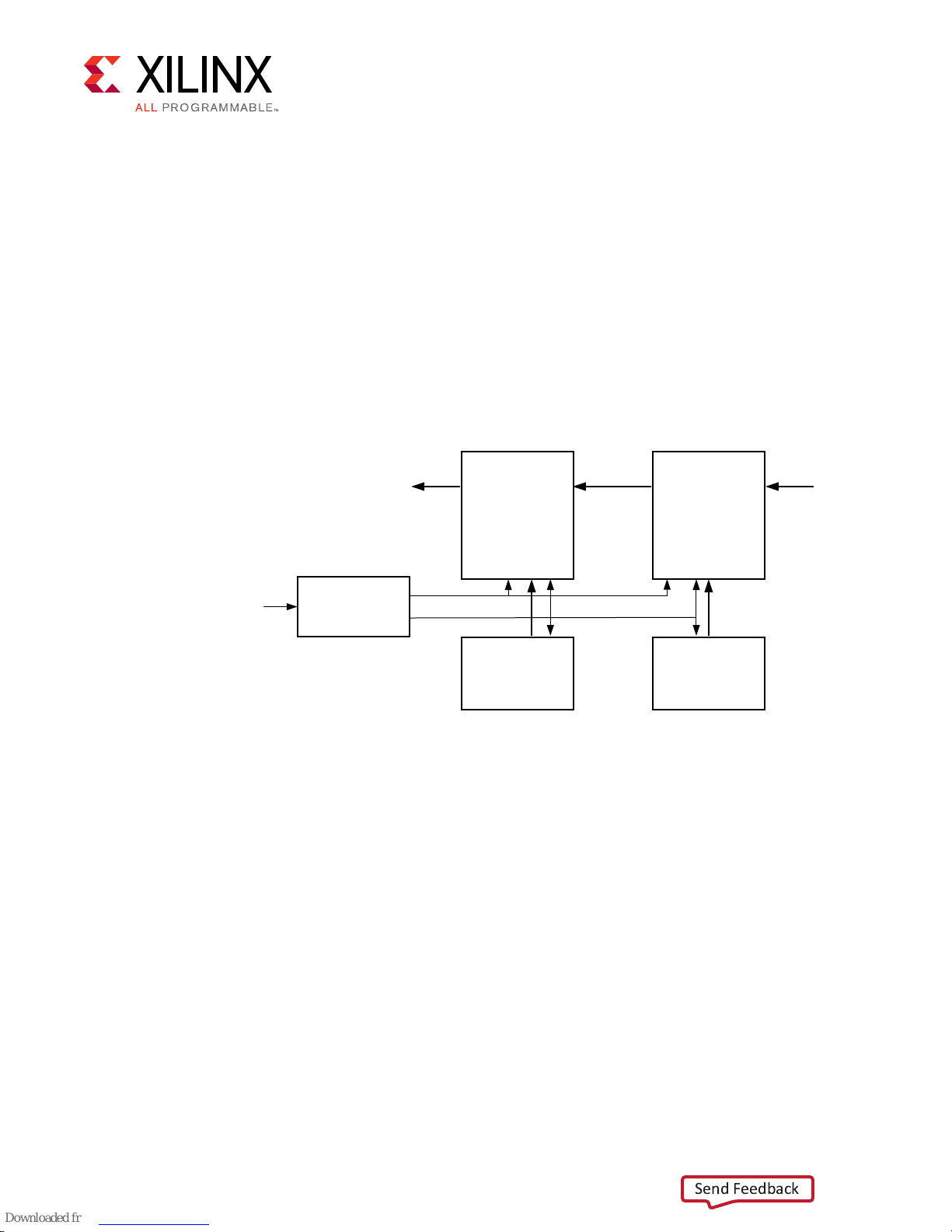
The I2S TX and RX IPs can be used in systems to send and receive I2S audio. A typical use case is
as shown below.
Figure 3: System Using TX RX
Chapter 4: Designing with the Core
Chapter 4
Audio
Source
Audio Sink I2S RX
AXIS
MCLK
AXIS
I2S TX
External
I2S DAC
External
I2S ADC
To Speakers or amp
Line in
X20719-042318
The I2S IPs typically interface with the external ADC/DAC which facilitates the playback of
audio.
PG308 (v1.0) April 4, 2018 www.xilinx.com [placeholder text]
I2S Transmitter and I2S Receiver 22
Page 23

Chapter 4: Designing with the Core
Send Feedback
General Design Guidelines
Use the Example Design
Each instance of the I2S Tramsmier and I2S Receiver core created by the Vivado design tool is
delivered with an example design that can be implemented in a device and then simulated. This
design can be used as a starng point for your own design or can be used to sanity-check your
applicaon in the event of diculty. See the Example Design content for informaon about using
and customizing the example designs for the core.
Related Informaon
Xilinx Resources
Registering Signals
To simplify ming and increase system performance in an programmable device design, keep all
inputs and outputs registered between the user applicaon and the core. This means that all
inputs and outputs from the user applicaon should come from, or connect to, a ip-op. While
registering signals might not be possible for all paths, it simplies ming analysis and makes it
easier for the Xilinx® tools to place and route the design.
Recognize Timing Critical Signals
The constraints provided with the example design idenfy the crical signals and ming
constraints that should be applied.
Related Informaon
Xilinx Resources
Make Only Allowed Modifications
You should not modify the core. Any modicaons can have adverse eects on system ming
and protocol compliance. Supported user conguraons of the core can only be made by
selecng the opons in the customizaon IP dialog box when the core is generated.
PG308 (v1.0) April 4, 2018 www.xilinx.com [placeholder text]
I2S Transmitter and I2S Receiver 23
Page 24
Chapter 4: Designing with the Core
Send Feedback
Clocking
There are three possible clock inputs available. Ensure that a proper aud_clk is supplied so that
the correct SCLK can be generated by the IP. Audio Clock is typically an interger mulple of
128×Fs and is decided by the DAC/ADC being used. It is advisable to use a very stable clock
source to generate the Audio Clock so as to minimize jier.
Table 26: Clocks
Clock Description
s_axi_ctrl_aclk Control interface clock
s_axis_aud_aclk AXIS streaming clock
m_axis_aud_aclk AXIS streaming clock
aud_aclk A reference audio clock which is an integer multiple of Fs
(typically 128×Fs, 384×Fs etc)
Resets
The s_axi_ctrl_aresetn resets the register interface and puts all the registers in their
default state.
The aud_mrst (an Acve-High reset) resets the audio domain, while the
s_axis_aud_aresetn resets the AXIS domain. Aer a reset, it is advisable to disable and
enable the IP for a clean recovery.
Programmimg Sequence
The I2S Transmier can be setup using the following programming sequence:
1. Setup the Channel Mux registers, if required.
Note: It is not recommended to change this value at runme.
Program the SCLK Divider.
2.
Note: It is not recommended to change this value at runme.
Enable the core.
3.
The I2S Receiver can be setup using the following programming sequence:
Setup the Channel Mux registers, if required.
1.
PG308 (v1.0) April 4, 2018 www.xilinx.com [placeholder text]
I2S Transmitter and I2S Receiver 24
Page 25
CLK
TDATA[31:0]
TVALID
TREADY
TID[4:0]
Pre-emble = TData[3:0]
Channel Status = TData[30]
D
0
D
1
D
2
D
3
D
N
D
0
D
1
D
2
D
3
D
N
0 1 2 3 n 0 1 2 3 n
X Y X Y Y Z Y Z Y Y
C[190] C[191] C[191] C[0] C[0]
Frame 191 (End of Block) Frame 0 (Start of Block)
Chapter 4: Designing with the Core
Send Feedback
Note: It is not recommended to change this value at runme.
2. Program the SCLK Divider.
Note: It is not recommended to change this value at runme.
3. Program the AES registers to specify the 192 bits of Channel Status value
4. Enable the core and latch the AES Channel bit.
Note: Aer asserng either aud_mrst or m_axis_aresetn, the core has to disabled and enabled again.
Interrupts
Each core has one interrupt output. The Interrupt output is level triggered and stays asserted
unl the interrupt status bits are cleared.
Audio AXIS Interface
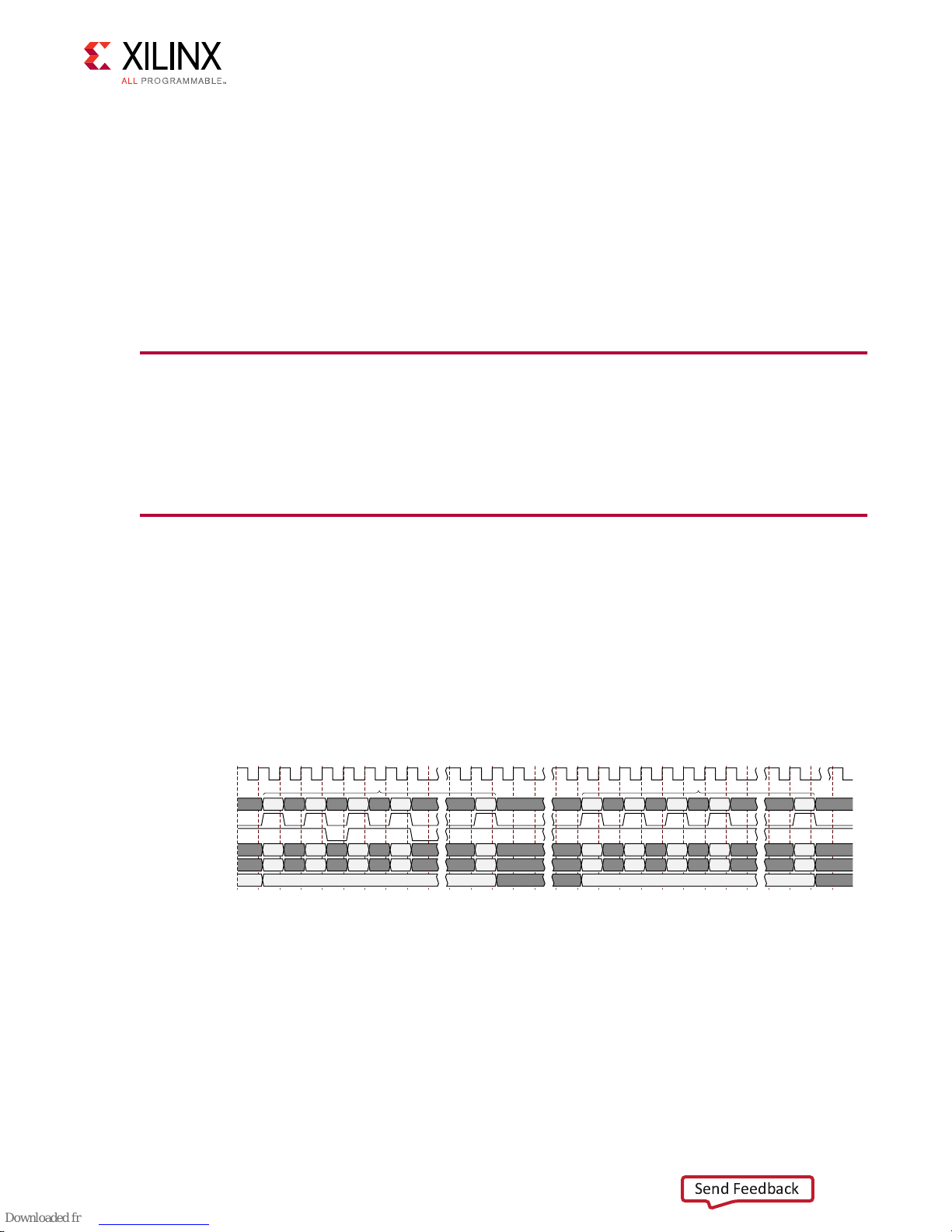
An AXI4-Stream audio cycle is illustrated in the following gure. The data is valid when both the
valid (TVLD) and ready (TRDY) signals are asserted. The I2S Receiver sends out adjacent channels
in sequenal order (CH0, CH1, etc). Usually, the I2S Transmier also expects the channels in
sequenal order. If the channel data is not in order, then the I2S Transmier would assert
underow or block sync error.
Figure 4: Audio AXIS Interface
You must ensure proper pre-emble and TIDs while sending more than two channels of Audio
data over AXIS. The data width over the AXI4-Stream interface is xed at 32-bits. All bit
posions are as per the IEC60958-3 standard except for the preamble bit format. The preamble
provides the start of the audio block and audio channel informaon. The preamble paerns for
the start of block, channelA audio data, and channelB audio data are listed as follows:
PG308 (v1.0) April 4, 2018 www.xilinx.com [placeholder text]
I2S Transmitter and I2S Receiver 25
Page 26

Table 27: Audio Axis Interface Patterns
Send Feedback
Bits [3:0] Description
0001 Start of Audio Block/Channel 0 Audio sample
0010 Channel 0/2/4/6 Audio data
0011 Channel 1/3/5/7 Audio data
Chapter 4: Designing with the Core
PG308 (v1.0) April 4, 2018 www.xilinx.com [placeholder text]
I2S Transmitter and I2S Receiver 26
Page 27

Design Flow Steps
Send Feedback
This secon describes customizing and generang the core, constraining the core, and the
simulaon, synthesis and implementaon steps that are specic to this IP core. More detailed
informaon about the standard Vivado® design ows and the IP integrator can be found in the
following Vivado Design Suite user guides:
• Vivado Design Suite User Guide: Designing IP Subsystems using IP Integrator (UG994)
• Vivado Design Suite User Guide: Designing with IP (UG896)
• Vivado Design Suite User Guide: Geng Started (UG910)
• Vivado Design Suite User Guide: Logic Simulaon (UG900)
Chapter 5
Customizing and Generating the Core
The I2S Transmier and Receiver can be found under the following Audio Connecvity and
Processing Vivado® IP catalog.
To access the I2S IPs, do the following:
1. Open an exisng project or create a new project using the Vivado design tools.
2. Open the IP catalog and navigate to the taxonomies.
3. Double-click on either I2S Receiver or Transmier to bring up the customize IP window.
For details, see the Vivado Design Suite User Guide: Designing with IP (UG896) and the Vivado
Design Suite User Guide: Geng Started (UG910).
Note: Figures in this chapter are illustraons of the Vivado Integrated Design Environment (IDE). This
layout might vary from the current version.
For more informaon on generang the core in the Vivado IP integrator, see the Vivado Design
Suite User Guide: Designing IP Subsystems using IP Integrator (UG994) for detailed informaon.
Vivado IDE might auto-compute certain conguraon values when validang or generang the
design, as noted in this secon. You can view the parameter value aer successful compleon of
the validate_bd_design command.
PG308 (v1.0) April 4, 2018 www.xilinx.com [placeholder text]
I2S Transmitter and I2S Receiver 27
Page 28

I2S Receiver Customize IP
Send Feedback
Figure 5: I2S Receiver Configuration Tab
Chapter 5: Design Flow Steps
PG308 (v1.0) April 4, 2018 www.xilinx.com [placeholder text]
I2S Transmitter and I2S Receiver 28
Page 29

Chapter 5: Design Flow Steps
Send Feedback
Figure 6: I2S Transmitter Configuration Tab
Field Descriptions
• Component Name : The base name of the output les generated for the core. Names must
begin with a leer and can be composed of any of the following characters: a- z, 0 to 9, and
"_".
• Audio Channels : Specify the number of Audio Channels. Allowed values are 2, 4, 6 and 8.
• I2S Data Width : Specify the I2S data width. Allowed values are 16 and 24.
• FIFO Depth : Specify the depth of the FIFO. Allowed values are 64, 128, 256, 512 and 1024.
In case of I2S Transmier, the data is output on I2S interface only aer the FIFO if half lled.
• Enable FIFO Data Count: Select this opon to enable the IP to output the FIFO Read data
count.
PG308 (v1.0) April 4, 2018 www.xilinx.com [placeholder text]
I2S Transmitter and I2S Receiver 29
Page 30

Chapter 5: Design Flow Steps
Send Feedback
User Parameters
The following table shows the relaonship between the elds in the Vivado IDE and the User
Parameters (which can be viewed in the tool command language (Tcl) Console).
Table 28: User Parameters
Vivado IDE Parameters Parameter Name Default Value Allowed Value
I2S Receiver
Audio Channels C_NUM_CHANNELS 2 2, 4, 6, 8
I2S Data width C_DWIDTH 24 16, 24
FIFO Depth C_DEPTH 128 64, 128, 256, 512, 1024
I2S Transmitter
Audio Channels C_NUM_CHANNELS 2 2, 4, 6, 8
I2S Data width C_DWIDTH 24 16, 24
FIFO Depth C_DEPTH 128 64, 128, 256, 512, 1024
Enable FIFO Count C_ENABLE_FIFO_COUNT False True, False
Output Generation
For details, see the Vivado Design Suite User Guide: Designing with IP (UG896).
Constraining the Core
Required Constraints
This secon is not applicable for this IP core.
Device, Package, and Speed Grade Selections
This secon is not applicable for this IP core.
Clock Frequencies
For more informaon, see Clocking.
Clock Management
It is advisable to have the Audio Clock generated from a stable source for minimal jier. If the
jier is of low importance, a MMCM can be used to generate the Audio clock.
PG308 (v1.0) April 4, 2018 www.xilinx.com [placeholder text]
I2S Transmitter and I2S Receiver 30
Page 31

Chapter 5: Design Flow Steps
Send Feedback
Clock Placement
Audio Clock, if supplied from an external source, should be connected to a clock capable IO so
that it can be used by FPGA fabric.
Banking
This secon is not applicable for this IP core.
Transceiver Placement
This secon is not applicable for this IP core.
I/O Standard and Placement
This secon is not applicable for this IP core.
Simulation
For comprehensive informaon about Vivado® simulaon components, as well as informaon
about using supported third-party tools, see the Vivado Design Suite User Guide: Logic Simulaon
(UG900).
Synthesis and Implementation
For details about synthesis and implementaon, see the Vivado Design Suite User Guide: Designing
with IP (UG896).
PG308 (v1.0) April 4, 2018 www.xilinx.com [placeholder text]
I2S Transmitter and I2S Receiver 31
Page 32
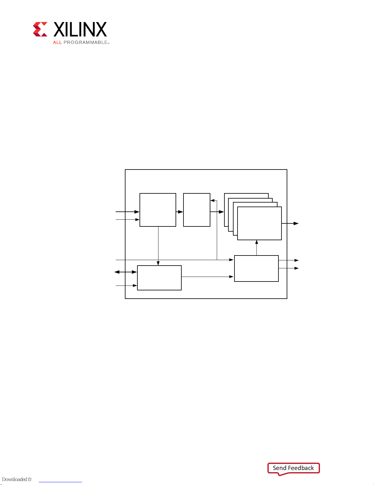
Example Design
Send Feedback
This chapter contains informaon about the example design provided in the Vivado Design Suite.
The top module instanates all components of the core and example design that are needed to
implement the design in hardware, as shown below. This includes Clocking Wizard and Register
conguraon modules.
Figure 7: Core Example Design
Chapter 6: Example Design
Chapter 6
AXIS I2S AXIS
I2S
Transmitter
AXI4 Lite
X20716-042318
Ref Clk In
Clock Gen
I2S Receiver
Aud_clk
AXI_clk
AXI4 Lite
ATG ATG
This example design demonstrates transacons on the AXI4-Lite and AXI4-Stream interfaces of
the DUT.
• Clock generator: A clocking wizard is used to generate the clocks for the example design. It
generates the aud_clk, AXI4-Lite clock, and the AXI4-Stream clock. The example design is
held in reset unl the MMCM is locked.
• Axi Trac Generator (ATG): The ATGs are used to program the I2S IPs. The ATGs start the
conguraon process as soon as the MMCM is locked.
• I2S Transmier: This module receives the Audio data and send it over to I2S bus, that is
connected to the I2S receiver.
• I2S Receiver: This module receives the I2S data and outputs it on the AXIS interface.
PG308 (v1.0) April 4, 2018 www.xilinx.com [placeholder text]
I2S Transmitter and I2S Receiver 32
Page 33

Chapter 6: Example Design
Send Feedback
Implementing the Example Design
For details about synthesis and implementaon, see the Vivado Design Suite User Guide: Designing
with IP (UG896).
Aer following the steps described in Chapter 5: Design Flow Steps, implement the example
design as follows:
1. Right-click the core in the Hierarchy window, and select Open IP Example Design.
2. A new window pops up, asking you to specify a directory for the example design. Select a
new directory, or keep the default directory. A new project is automacally created in the
selected directory and opened in a new Vivado IDE window.
3. In the Flow Navigator (le-side pane), click Run Implementaon and follow the direcons. In
the current project directory, a new project with the name _ex0 is created and the les are
delivered in that directory. This directory and its subdirectories contain all the source les
that are required to create the AXI MCDMA controller example design.
Simulating the Example Design
Using the AXI MCDMA example design (delivered as part of the AXI MCDMA), the behavior of
the AXI MCDMA can be quickly simulated and observed. The simulaon script compiles the AXI
MCDMA example design and the supporng simulaon les. It then runs the simulaon and
checks if it completed successfully.
If the test fails, the following message displays: Test Failed!!!
If the test passes, the following message displays: Test Completed Successfully
If the test hangs, the following message displays: Test Failed!! Test Timed Out
PG308 (v1.0) April 4, 2018 www.xilinx.com [placeholder text]
I2S Transmitter and I2S Receiver 33
Page 34
Chapter 6: Example Design
Send Feedback
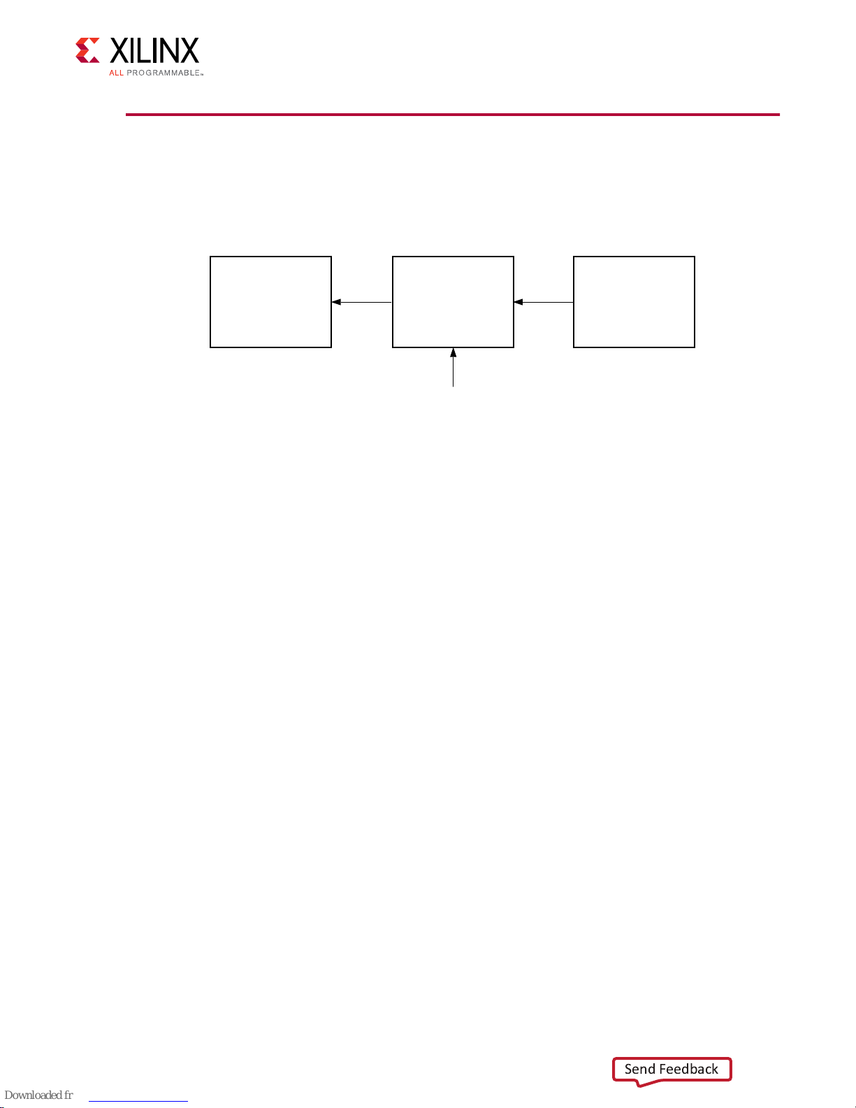
Test Bench for Example Design
This secon contains informaon about the provided test bench in the Vivado Design Suite
Figure 8: Test Bench
AXIS Data
Checker
AXIS AXIS
EXDES
Clk_in
AXIS Data
Generator
X20718-042318
The above gure shows the test bench for example design. The top-level test bench feeds a clock
input, AXIS data to the exdes. The TB also checks the received AXIS data
• AXIS Data Generator: This module generates the AXIS Audio trac and feeds the I2S
Transmier.
• AXIS Data Checker: This modules reads the AXIS data and check for data integrity.
PG308 (v1.0) April 4, 2018 www.xilinx.com [placeholder text]
I2S Transmitter and I2S Receiver 34
Page 35

Debugging
Send Feedback
This appendix includes details about resources available on the Xilinx Support website and
debugging tools.
If the IP requires a license key, the key must be veried. The Vivado® design tools have several
license checkpoints for gang licensed IP through the ow. If the license check succeeds, the IP
can connue generaon. Otherwise, generaon halts with error. License checkpoints are
enforced by the following tools:
• Vivado Synthesis
• Vivado Implementaon
• write_bitstream (Tcl command)
Note: IP license level is ignored at checkpoints. The test conrms a valid license exists. It does not check IP
license level.
Appendix A
Finding Help on Xilinx.com
To help in the design and debug process when using the core, the Xilinx Support web page
contains key resources such as product documentaon, release notes, answer records,
informaon about known issues, and links for obtaining further product support.
Documentation
This product guide is the main document associated with the core. This guide, along with
documentaon related to all products that aid in the design process, can be found on the Xilinx
Support web page or by using the Xilinx® Documentaon Navigator. Download the Xilinx
Documentaon Navigator from the Downloads page. For more informaon about this tool and
the features available, open the online help aer installaon.
PG308 (v1.0) April 4, 2018 www.xilinx.com [placeholder text]
I2S Transmitter and I2S Receiver 35
Page 36

Appendix A: Debugging
Send Feedback
Answer Records
Answer Records include informaon about commonly encountered problems, helpful informaon
on how to resolve these problems, and any known issues with a Xilinx product. Answer Records
are created and maintained daily ensuring that users have access to the most accurate
informaon available.
Answer Records for this core can be located by using the Search Support box on the main Xilinx
support web page. To maximize your search results, use keywords such as:
• Product name
• Tool message(s)
• Summary of the issue encountered
A lter search is available aer results are returned to further target the results.
Master Answer Record for the Core
For I2S Receiver, see Xilinx Answer 70288
For I2S Transmier, see Xilinx Answer 70699
Technical Support
Xilinx provides technical support in the Xilinx Support web page for this LogiCORE™ IP product
when used as described in the product documentaon. Xilinx cannot guarantee ming,
funconality, or support if you do any of the following:
• Implement the soluon in devices that are not dened in the documentaon.
• Customize the soluon beyond that allowed in the product documentaon.
• Change any secon of the design labeled DO NOT MODIFY.
To contact Xilinx Technical Support, navigate to the Xilinx Support web page.
PG308 (v1.0) April 4, 2018 www.xilinx.com [placeholder text]
I2S Transmitter and I2S Receiver 36
Page 37

Appendix A: Debugging
Send Feedback
Hardware Debug
Hardware issues can range from no audio to audio with noise. This secon provides debug steps
for common issues.
Following are some of the common problems encountered and possible soluons:
1. No audio received/played: Ensure that the ADC/DAC/CODEC is in Slave mode. The I2S IPs
operate as Masters. The I2S IPs only support 16 or 24 bit I2S mode only.
2. Audio has a lot of noise: Ensure that DAC/ADC/CODEC are congured for the same data
width as the I2S IPs. Also ensure that the MCLK supplied to the DAC/ADC/CODEC is same
as the one supplied to I2S IPs.
PG308 (v1.0) April 4, 2018 www.xilinx.com [placeholder text]
I2S Transmitter and I2S Receiver 37
Page 38

Appendix B: Additional Resources and Legal Notices
Send Feedback
Appendix B
Additional Resources and Legal
Notices
Xilinx Resources
For support resources such as Answers, Documentaon, Downloads, and Forums, see Xilinx
Support.
Documentation Navigator and Design
Hubs
Xilinx® Documentaon Navigator provides access to Xilinx documents, videos, and support
resources, which you can lter and search to nd informaon. To open the Xilinx Documentaon
Navigator (DocNav):
• From the Vivado® IDE, select Help → Documentaon and Tutorials.
• On Windows, select Start → All Programs → Xilinx Design Tools → DocNav.
• At the Linux command prompt, enter docnav.
Xilinx Design Hubs provide links to documentaon organized by design tasks and other topics,
which you can use to learn key concepts and address frequently asked quesons. To access the
Design Hubs:
• In the Xilinx Documentaon Navigator, click the Design Hubs View tab.
• On the Xilinx website, see the Design Hubs page.
Note: For more informaon on Documentaon Navigator, see the Documentaon Navigator page on the
Xilinx website.
PG308 (v1.0) April 4, 2018 www.xilinx.com [placeholder text]
I2S Transmitter and I2S Receiver 38
Page 39

Appendix B: Additional Resources and Legal Notices
Send Feedback
References
These documents provide supplemental material useful with this product guide:
1. Vivado Design Suite User Guide: Designing IP Subsystems using IP Integrator (UG994)
2. Vivado Design Suite User Guide: Designing with IP (UG896)
3. Vivado Design Suite User Guide: Geng Started (UG910)
4. Vivado Design Suite User Guide: Logic Simulaon (UG900)
5. Vivado Design Suite User Guide: Programming and Debugging (UG908)
6. ISE to Vivado Design Suite Migraon Guide (UG911)
7. Vivado Design Suite User Guide: Implementaon (UG904)
Training Resources
1. Vivado Design Suite Hands-on Introductory Workshop
2. Vivado Design Suite Tool Flow
Revision History
The following table shows the revision history for this document.
Section Revision Summary
04/04/2018 v1.0
Initial Xilinx release.
PG308 (v1.0) April 4, 2018 www.xilinx.com [placeholder text]
I2S Transmitter and I2S Receiver 39
Page 40

Appendix B: Additional Resources and Legal Notices
Send Feedback
Please Read: Important Legal Notices
The informaon disclosed to you hereunder (the "Materials") is provided solely for the selecon
and use of Xilinx products. To the maximum extent permied by applicable law: (1) Materials are
made available "AS IS" and with all faults, Xilinx hereby DISCLAIMS ALL WARRANTIES AND
CONDITIONS, EXPRESS, IMPLIED, OR STATUTORY, INCLUDING BUT NOT LIMITED TO
WARRANTIES OF MERCHANTABILITY, NON-INFRINGEMENT, OR FITNESS FOR ANY
PARTICULAR PURPOSE; and (2) Xilinx shall not be liable (whether in contract or tort, including
negligence, or under any other theory of liability) for any loss or damage of any kind or nature
related to, arising under, or in connecon with, the Materials (including your use of the
Materials), including for any direct, indirect, special, incidental, or consequenal loss or damage
(including loss of data, prots, goodwill, or any type of loss or damage suered as a result of any
acon brought by a third party) even if such damage or loss was reasonably foreseeable or Xilinx
had been advised of the possibility of the same. Xilinx assumes no obligaon to correct any
errors contained in the Materials or to nofy you of updates to the Materials or to product
specicaons. You may not reproduce, modify, distribute, or publicly display the Materials
without prior wrien consent. Certain products are subject to the terms and condions of
Xilinx's limited warranty, please refer to Xilinx's Terms of Sale which can be viewed at hps://
www.xilinx.com/legal.htm#tos; IP cores may be subject to warranty and support terms contained
in a license issued to you by Xilinx. Xilinx products are not designed or intended to be fail-safe or
for use in any applicaon requiring fail-safe performance; you assume sole risk and liability for
use of Xilinx products in such crical applicaons, please refer to Xilinx's Terms of Sale which can
be viewed at hps://www.xilinx.com/legal.htm#tos.
AUTOMOTIVE APPLICATIONS DISCLAIMER
AUTOMOTIVE PRODUCTS (IDENTIFIED AS "XA" IN THE PART NUMBER) ARE NOT
WARRANTED FOR USE IN THE DEPLOYMENT OF AIRBAGS OR FOR USE IN APPLICATIONS
THAT AFFECT CONTROL OF A VEHICLE ("SAFETY APPLICATION") UNLESS THERE IS A
SAFETY CONCEPT OR REDUNDANCY FEATURE CONSISTENT WITH THE ISO 26262
AUTOMOTIVE SAFETY STANDARD ("SAFETY DESIGN"). CUSTOMER SHALL, PRIOR TO USING
OR DISTRIBUTING ANY SYSTEMS THAT INCORPORATE PRODUCTS, THOROUGHLY TEST
SUCH SYSTEMS FOR SAFETY PURPOSES. USE OF PRODUCTS IN A SAFETY APPLICATION
WITHOUT A SAFETY DESIGN IS FULLY AT THE RISK OF CUSTOMER, SUBJECT ONLY TO
APPLICABLE LAWS AND REGULATIONS GOVERNING LIMITATIONS ON PRODUCT
LIABILITY.
Copyright
© Copyright 2018 Xilinx, Inc. Xilinx, the Xilinx logo, Arx, ISE, Kintex, Spartan, Virtex, Vivado,
Zynq, and other designated brands included herein are trademarks of Xilinx in the United States
and other countries.All other trademarks are the property of their respecve owners.
PG308 (v1.0) April 4, 2018 www.xilinx.com [placeholder text]
I2S Transmitter and I2S Receiver 40
 Loading...