10/96
BLOCK DIAGRAM
• Combined DAC/Voltage
Monitor and PWM Functions
• 4-Bit Digital-to-Analog
Converter (DAC)
• 1.0% DAC/Reference
• Low Offset X20 Current Sense
Amplifier
• 100kHz, 200kHz, 400kHz
Oscillator Frequency Options
• Foldback Current Limiting
• Overvoltage and Undervoltage
Fault Windows
• Undervoltage Lockout
• 2Ω Totem Pole Output
• Chip Disable Function
Pentium® Pro Controller
FEATURES DESCRIPTI ON
UDG-96106-1
UCC2880-4/-5/-6
UCC3880-4/-5/-6
PRELIMINARY
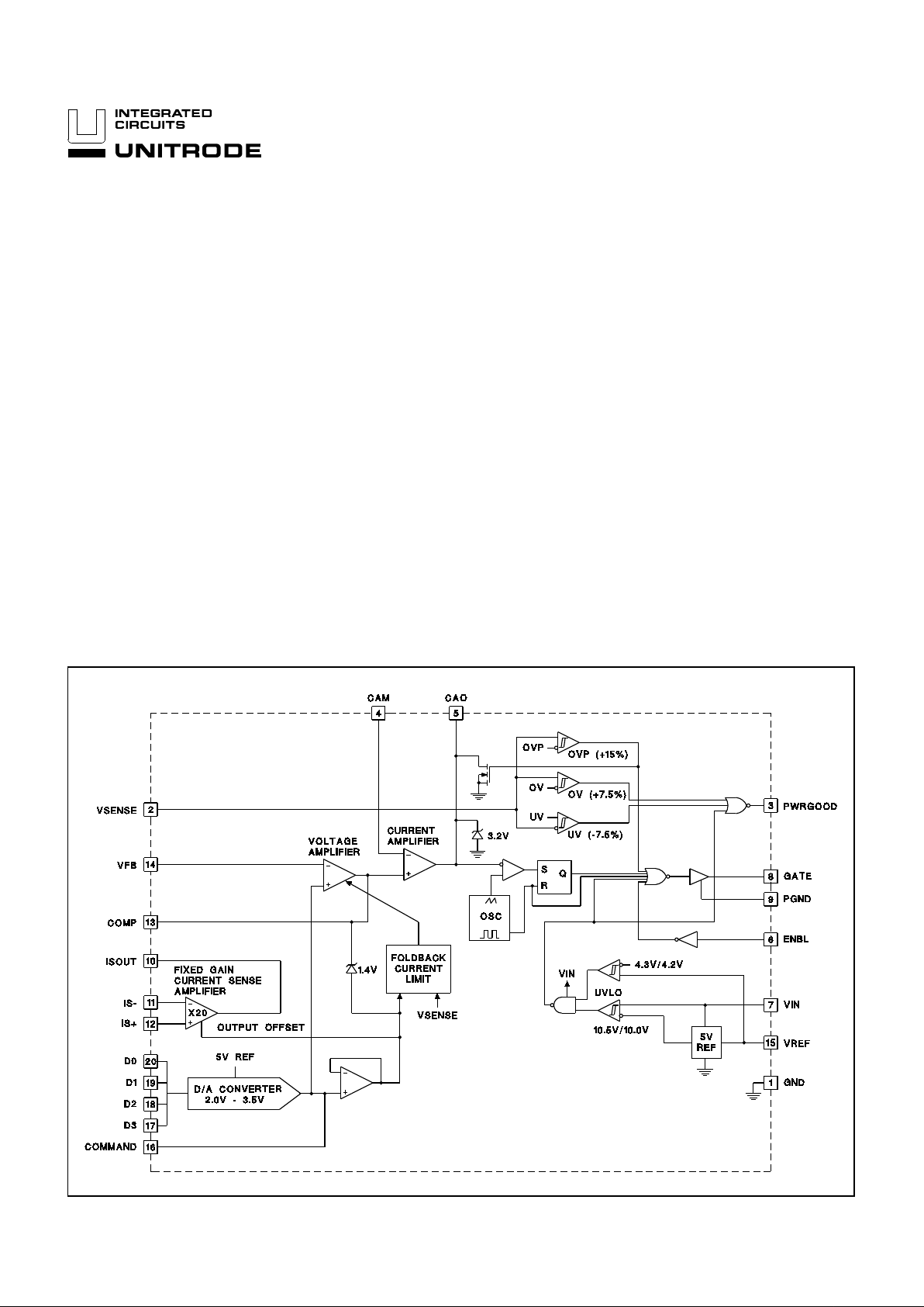
The UCC3880-4/-5/-6 combines high precision reference and voltage monitoring circuitry with average current mode PWM controller circuitry to power Intel
Pentium Pro and other high-end microprocessors with a minimum of external
components. The UCC3880-x converts 5VDC to an adjustable output, ranging
from 2.0VDC to 3.5VDC in 100mV steps with 1% DC system accuracy.
The chip incl udes a precision 5V reference which is capable of sourcing current to an external load. The output voltage of the DAC is derived from this
reference, and is programmed directly by Intel’ s VID pins (Table 1).
The accuracy of the DAC/reference combination is 1.0%. The overvoltage and
undervoltage comparators monitor the system output voltage and indicate
when it rises above or falls below its programmed value by more than 7.5%. A
second overvoltage protection comparator pulls the current amplifier output
voltage low to force zero duty cycle w hen the system output voltage exceeds
its designed value by more than 15%. This comparator also terminates the cycle. Undervoltage lockout circuitry assures the correct logic states at the outputs during powerup and powe rdown . Grounding the ENABLE pin forces the
GATE output low.
(continued)

UCC2880-4/-5/-6
UCC3880-4/-5/-6
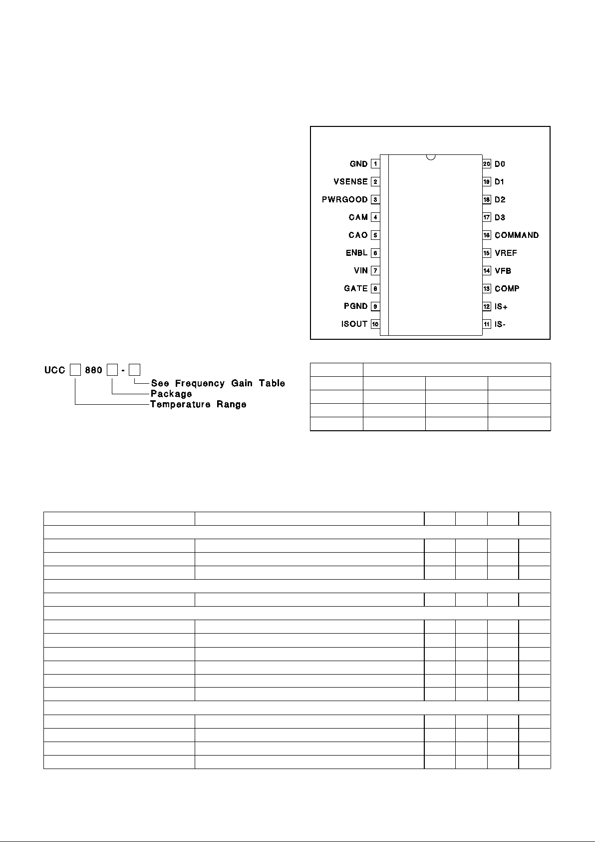
CONNECTION DIAG RAM
SOIC-20 (Top View)
DW Package
ELECTRICAL CHARACTE RIST I CS:
Unless otherwise specified, VIN = 12V, VSENSE = 3.5V, VENBL = 5V, VD0 = VD1 = VD2
= VD3 = 0V, 0°C < T
A < 70°C, TA = TJ.
PARAMETER TEST CONDITIONS MIN TYP MAX UNITS
Undervol ta ge Lockout
VIN UVLO Turn-on Thr esh old 10.5 10. 8 V
VIN UVLO Turn-off Threshold 9.5 10 V
UVLO Threshold Hysteresis 500 mV
Supply Cur ren t
l
IN 3.5 mA
DAC/Reference
COMMAND Voltage Accu rac y 10.8V < VIN < 13.2V, I
VREF = 0mA –1 1 %
D0-D3 Voltage High DX Pin Floating 5 V
D0-D3 Input Bias Curre nt DX Pin Tied to GND –70 –20 µA
VREF Output Voltage 4.975 5 5.025 V
VREF Load Regulat io n I
VREF = 0mA to 5mA –10 0 mV
VREF Sourcing Current VREF = 0V 10 mA
OVP Comparator
Trip Point % Over COMMAND Volt age 10 15 20 %
Hystere s is 20 30 mV
VSENSE Input Bias Current OV, OVP, UV Combined –0.1 µA
Propagation Delay 1 µs
The voltage and current amplifiers have a 4MHz gain
bandwidth p roduct to satisfy high performance system requirements. The internal current sense amplifier permits
the use of a low val ue current sense resistor, minimizing
power loss. The oscillator frequency is fixed internally at
100kHz, 200kHz, or 400kHz, depending upon the option
selected. The foldback circuit reduces the converter short
circuit current limit to 50% of its nominal value when the
converter is short circuited. The gate driver is a 2Ω totem
pole output stage capable of driving an external MOSFET.
This device is available in 20-pin dual i n-line and surface
mount packa ges. The UCC2880-x is specifie d for operation from –25°C to 85°C, and the UCC3880-x is specified
for operation from 0°C to 70°C.
Pentium® Pro is a registered trademark of Intel Corporation.
DESCRIPTION (cont. )
Frequency
100kHz 200kHz 400kHz
UCC3880-4 X
UCC3880-5 X
UCC3880-6 X
Frequency Gain Table
ORDERING INFORMATION
Consult factory f or temper at ure ran ge or package opt ions
not shown.
2

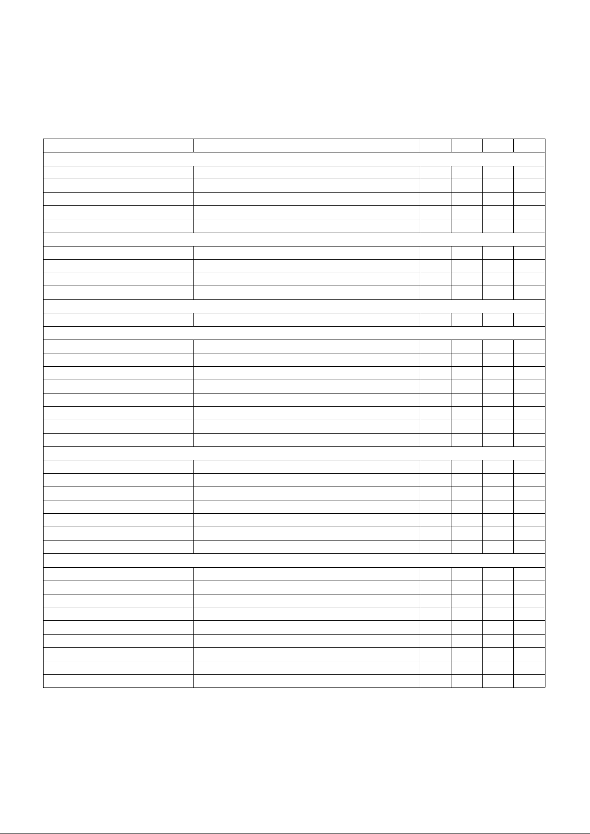
ELECTRICAL CHARACTE RISTICS (cont.): Unless otherw ise specified, VIN = 12V, VSENSE = 3.5V, VENBL = 5V, VD0 =
VD1 = VD2 = VD3 = 0V, 0°C < T
A < 70°C, TA = TJ.
PARAMETER TEST CONDIT IONS MI N TYP MAX UNIT S
OV Comparator
Trip Point % Over COMMAND Voltage ( Not e 1) 7.6 10 %
Return Point % Over COMMAND Voltage ( Not e 1) 5 7.4 %
Hystere sis 20 30 mV
PWRGOOD Equiva lent Resist ance VSENSE = 2.0V 470 Ω
Propagation Delay 1 µs
UV Comparator
Trip Point % Over COMMAND Voltage ( Not e 1) –10 –7.6 %
Return Point % Over COMMAND Voltage ( Not e 1) –7.4 – 5 %
Hystere sis 20 30 mV
Propagation Delay 1 µs
Enable Pi n
Pull-up Cur ren t V
ENBL = 2.5V –50 –20 µA
Voltage Error Amplifier
Input Offset Voltage V
COMP = 3.5V 0.0 mV
Input Bias Current V
CM = 3.0V –0.0 2 0 µA
Open Loo p Ga in 1V < V
COMP < 4V 90 dB
Common Mode Rejection Rat i o 2V < V
COMP < 3.5V 90 dB
Power Supply Reject ion Rat i o 10.8V < VIN < 15 V 85 dB
Output Sourcing Current V
VFB = 2V, VCOMMAND = VCOMP = 2.5V –0.5 mA
Output Sinking Current V
VFB = 3V, VCOMMAND = VCOMP = 2.5V 2.0 mA
Gain Bandwidth Product F = 100kHz 3 MHz
Current Sense Amplifier
Gain 20 V/V
Input Resistance 5kΩ
Common Mode Rejection Rat i o 0V < V
CM < 4.5V 60 dB
Power Supply Reject ion Rat i o 10.8V < VIN < 15 V 80 dB
Output Sourcing Current V
IS– = 2V, VISOUT = VIS+ = 2.5V –0.5 mA
Output Sinking Current V
IS– = 3V, VISOUT = VIS+ = 2.5V 6.0 mA
–3dB Freque ncy At GAIN = 20 1.75 MHz
Current Amplifier
Input Offset Voltage V
CM = 3.0V 10 mV
Input Bias Current V
CM = 3.0V 0.15 µA
Open Loo p Ga in 1V < V
CAO < 3V 90 dB
Output Voltage High VCOMP = 3V, VCAM = 2.5V 3.2 V
Common Mode Rejection Rat i o 1.5V < V
CM < 4.9V 80 dB
Power Supply Reject ion Rat i o 10.8V < VIN < 15 V 80 dB
Output Sourcing Current V
CAM = 2V, VCAO = VCOMP = 2.5V –0.5 mA
Output Sinking Current V
CAM = 3V, VCAO = VCOMP = 2.5V 2.0 mA
Gain Bandwidth Product F = 100kHz 3.5 MHz
UCC2880-4/-5/-6
UCC3880-4/-5/-6
3
 Loading...