Texas Instruments UC39431N, UC39431DTR, UC39431D, UC29431DTR, UC29431D Datasheet
...
UC19431
UC29431
UC39431
UC39431B
DESCRIPTION
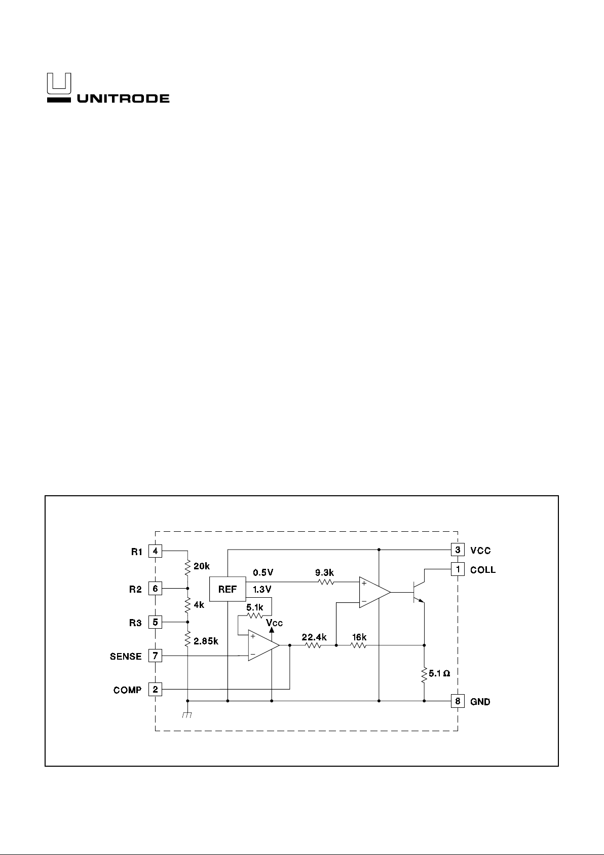
The UC39431 is an adjustable shunt voltage regulator with 100mA sink ca
pability. The architecture, comprised of an error amplifier and
transconductance amplifier, gives the user separate control of the small
signal error voltage frequency response along with a fixed linear
transconductance. A minimum 3MHz gain bandwidth product for both the
error and transconductance amplifiers assures fast response. In addition to
external programming, the IC has three internal resistors that can be con
nected in six different configurations to provide regulated voltages of 2.82V,
3.12V, 5.1V, 7.8V, 10.42V, and 12.24V. A sister device (UC39432) provides
access to the non-inverting error ampilifer input and reference, while elimi
nating the three internal resistors.
Precision Adjustable Shunt Regulator
FEATURES
•
Multiple On-Chip Programmable
Reference Voltages
•
0.4% Initial Accuracy
•
0.7% Overall Reference Tolerance
•
2.2V to 36.0V Operating Supply
Voltage and User Programmable
Reference
•
36.0V Operating Supply Voltage
•
Reference Accuracy Maintained For
Entire Range of Supply Voltage
•
Superior Accuracy and Easier
Compensation for Optoisolator
Application
• Improved Architecture Provides a
Known Linear Transconductance with
a +5% Typical Tolerance
04/99
BLOCK DIAGRAM
UDG-95087

2
UC19431
UC29431
UC39431
UC39431B
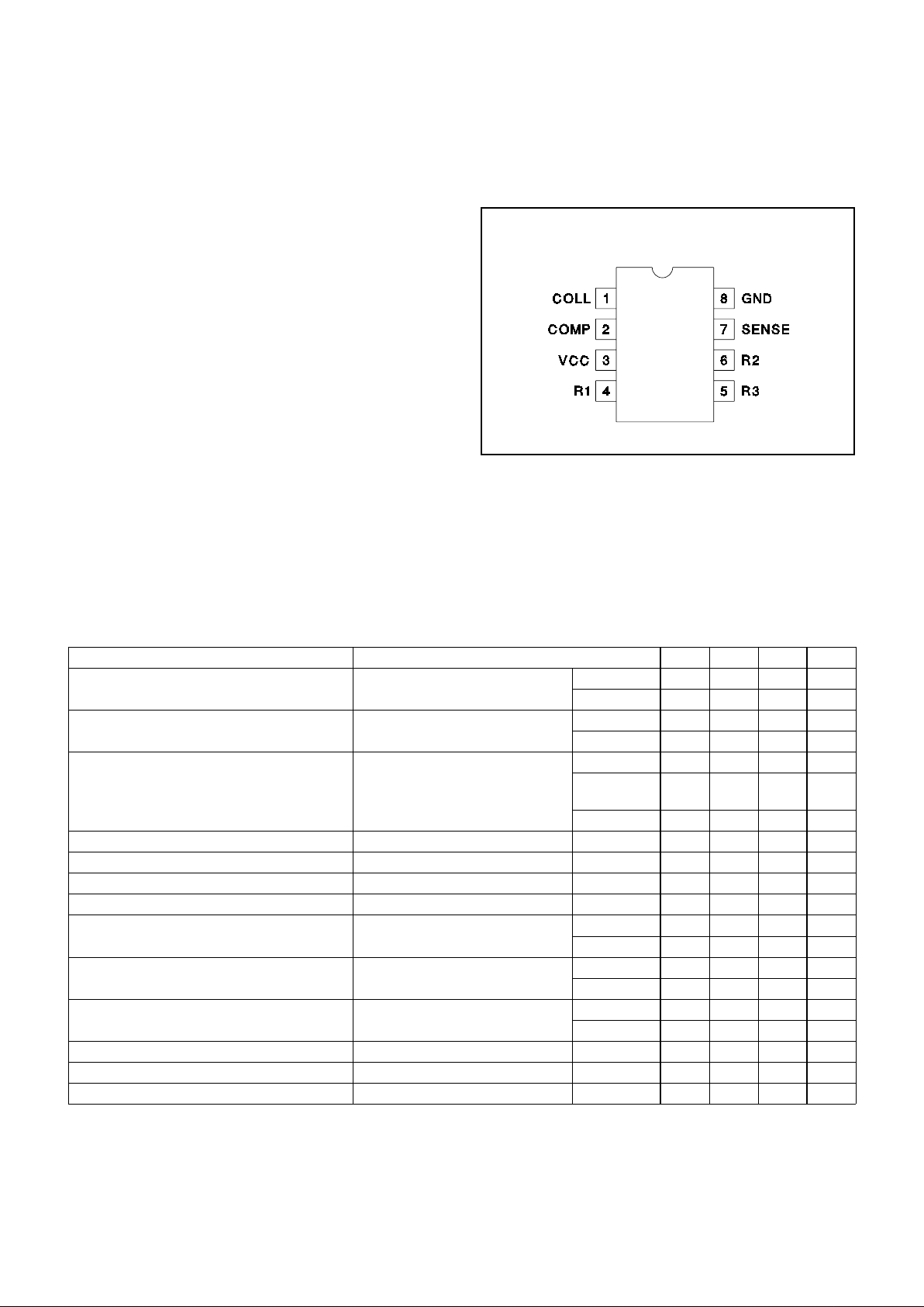
DIL-8, SOIC-8 (Top View)
N or J, D Package
ABSOLUTE MAXIMUM RATINGS
Supply Voltage: V . . . . . . . . . . . . . . . . . . . . . . . . . . . . . 36V
Regulated Output: V . . . . . . . . . . . . . . . . . . . . . . . . . . . . . . 36V
Internal Resistors: R1, R2, R3. . . . . . . . . . . . . . . . . . . . . . . 13V
E/A Input: SENSE . . . . . . . . . . . . . . . . . . . . . . . . . . . . . . . . . 6V
E/A Compensation: COMP . . . . . . . . . . . . . . . . . . . . . . . . . . 6V
Output Sink Current: I. . . . . . . . . . . . . . . . . . . . . . . . . . . 140mA
Power Dissipation at T
A
≤25°C (DIL-8). . . . . . . . . . . . . . . . . 1W
Derate 8mW/°C for T
A
> 25°C
Storage Temperature Range . . . . . . . . . . . . . –65°C to +150°C
Junction Temperature. . . . . . . . . . . . . . . . . . . –55°C to +150°C
Lead Temperature (Soldering, 10 sec.). . . . . . . . . . . . . +300°C
Currents are positive into, negative out of the specified termi
-
nal. Consult Packaging Section of Databook for thermal limita
-
tions and considerations of packages.
ELECTRICAL CHARACTERISTICS: Unless otherwise stated, these specifications apply for T
A
= –55°C to +125°C and
COLL Output = 2.4V to 36.0V for the UC19431, T
A
= –25°C to +85°C and COLL Output = 2.3V to 36.0V for the UC29431, and T
A
= 0°C to +70°C and COLL Output = 2.3V to 36.0V for the UC39431/B, VCC = 15V, I
COLL
= 10mA, TA=TJ.
PARAMETER
TEST CONDITIONS
MIN TYP MAX UNITS
Reference Voltage Tolerance T
A
= 25°C 19431* 1.295 1.3 1.305 V
39431B 1.29 1.3 1.31 V
Reference Temperature Tolerance V
COLL
= 5.0 19431* 1.291 1.3 1.309 V
39431B 1.286 1.3 1.314 V
Reference Line Regulation
Reference Load Regulation
VCC = 2.2V to 36.0V, V
COLL
= 5V
I
COLL
= 10mA to 50mA, V
COLL
= 5V
19431* 10 38 mV
39431B
19431*
10
10
5738mV
mV
39431B 10 57 mV
Sense Input Current –0.5 –0.2 µA
Minimum Operating Current VCC = 36.0V, V
COLL
= 5V 0.50 0.80 mA
Collector Current Limit V
COLL
= VCC = 36.0V, Ref = 1.35V 130 145 mA
Collector Saturation I
COLL
= 20mA 0.7 1.1 1.5 V
Transconductance (gm) VCC = 2.4V to 36.0V,
V
COLL
= 3V, I
COLL
= 20mA
19431* –170 –140 –110 mS
39431B –180 –140 –100 mS
5.1V Reference Internal Divider 19431* 5.05 5.1 5.15 V
39431B 5 5.1 5.2 V
12.24V Reference Internal Divider 19431* 12 12.24 12.5 V
39431B 12 12.24 12.5 V
Error Amplifier AVOL 60 90 dB
Error Amplifier GBW (Note 1) 3.0 5 MHz
Transconductance Amplifier GBW 3 MHz
* Also applies to the UC29431 and UC39431
Note: The internal divider can be configured to give six unique references.These references are 2.82V, 3.12V, 5.1V, 7.8V,
10.42V, 12.24V.
Note 1: Guaranteed by design.Not 100% tested in production.
CONNECTION DIAGRAM

3
UC19431
UC29431
UC39431
UC39431B
COLL: The collector of the output transistor with a maxi
mum voltage of 36V. This pin is the output of the
transconductance amplifier. The overall open loop volt
age gain of the transconductance amplifier is gm • RL,
where gm is designed to be –140mS ±30mS and RL rep
resents the output load.
COMP: The output of the error amplifier and the input to
the transconductance amplifier. This pin is available to
compensate the high frequency gain of the error ampli
fier.It is internally voltage limited to approximately 2.0V.
GND: The reference and power ground for the device.
The power ground of the output transistor is isolated on
the chip from the substrate ground used to bias the re
mainder of the device.
R1, R2, R3: Connection points to the three internal resis
tors.
SENSE: The inverting terminal of the error amplifier used
as both the voltage sense input to the error amplifier and
its other compensation point. The error amplifier uses the
SENSE input to compare against the 1.3V on-chip reference.
The SENSE pin is also used as the undervoltage lockout
(UVLO). It is intended to keep the chip from operating un
-
til the internal reference is properly biased. The thresh
old is approximately 1V. It is important that once the
UVLO is released, the error amplifier can drive the
transconductance amplifier to stabilize the loop. If a ca
pacitor is connected between the SENSE and COMP
pins to create a pole, it will limit the slew rate of the error
amplifier. To increase the bandwidth and ensure startup
at low load current, it is recommended to create a zero
along with the pole as shown in the shunt regulator appli
cation. The error amplifier must slew 2.0V to drive the
transconductance amplifier initially on.
VCC: The power connection for the device.The minimum
to maximum operating voltage is 2.2V to 36.0V. The qui
escent current is typically 0.50mA.
PIN DESCRIPTIONS (cont.)
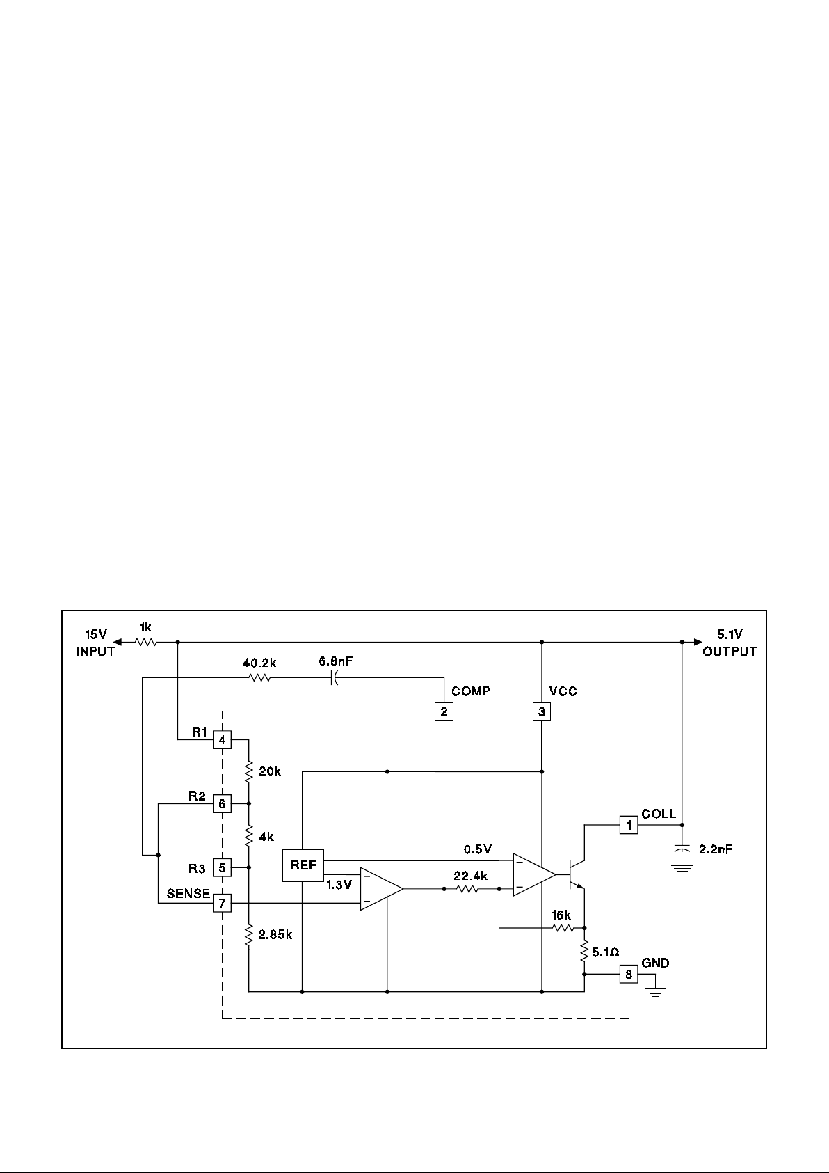
Figure 1. Typical 5.1V shunt regulator application.
UDG-95088
 Loading...