9/94
• Optimized for Off-line and DC to DC
Converters
• Low Start Up Current (<0.5mA)
• Trimmed Oscillator Discharge Current
• Automatic Feed Forward Compensation
• Pulse-by-Pulse Current Limiting
• Enhanced Load Response Characteristics
• Under-Voltage Lockout With Hysteresis
• Double Pulse Suppression
• High Current Totem Pole Output
• Internally Trimmed Bandgap Reference
• 500kHz Operation
• Low R
O Error Amp
Current Mode PWM Controller
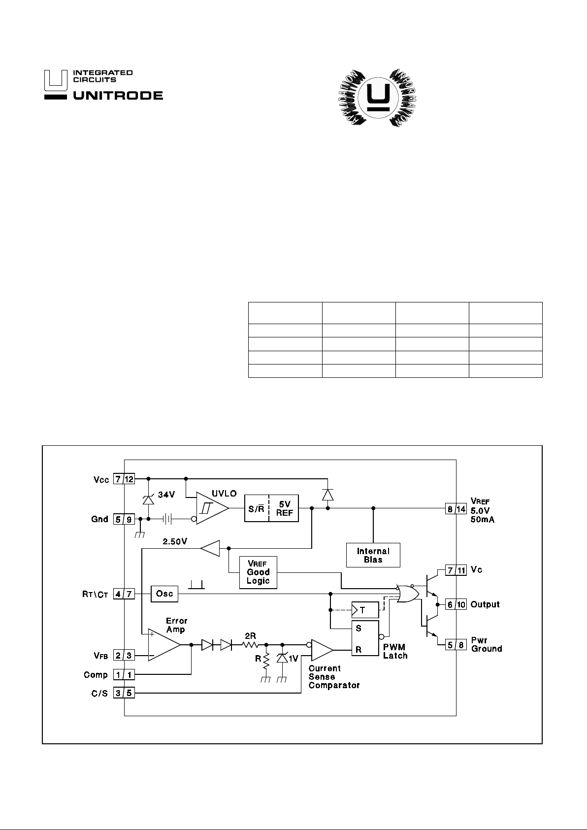
The UC1842A/3A/4A/5A family of control ICs is a pin for pin compatible improved versi on of th e UC3842 /3/4/5 family. Providing the necessary features to control current mode switched mode power
supplies, this family has the following improved features. Start up current is guaranteed to be less than 0.5mA. Oscillator discharge is
trimmed to 8.3mA. During under voltage lockout, the output stage can
sink at least 10mA at less than 1.2V for V CC over 5 V.
The difference between members of this family are shown in the table
below.
UC1842A/3A/4A/5A
UC2842A/3A/4A/5A
UC3842A/3A/4A/5A
BLOCK DIAGRAM
FEATURES DESCRIPTION
Part # UVLO On UVLO Off
Maximum Duty
Cycle
UC1842A 16.0V 10.0V <100%
UC1843A 8.5V 7.9V <100%
UC1844A 16.0V 10.0V <50%
UC1845A 8.5V 7.9V <50%
Note 1: A = DIL-8 Pin Number. B = SO-14 Pin Num be r .
Note 2: Toggle f lip flop use d only in 1844A and 1845A.
A/B

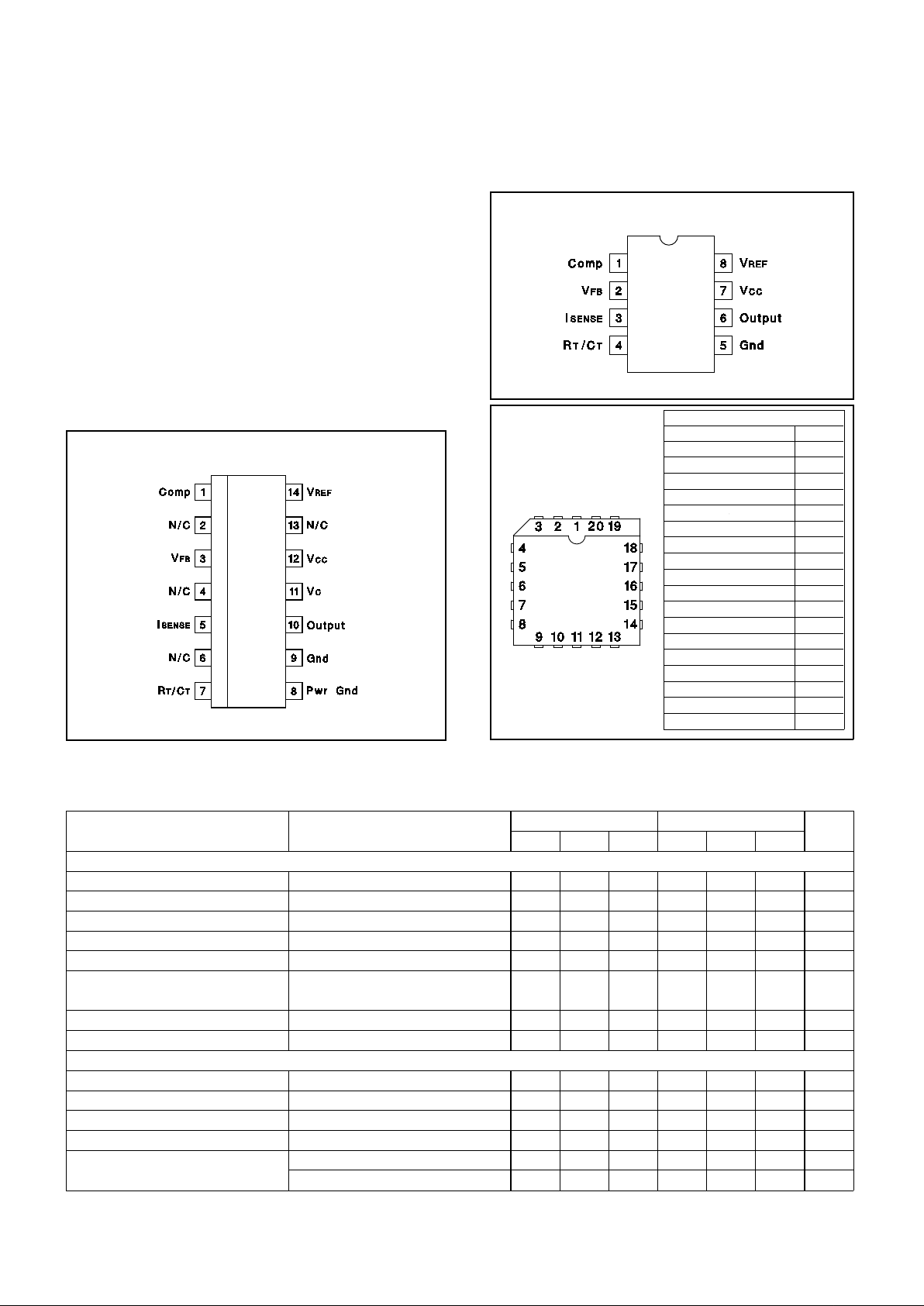
PACKAGE PIN FUNCTION
FUNCTION PIN
N/C
1
Comp 2
N/C 3-4
VFB 5
N/C 6
ISENSE 7
N/C 8-9
RT/CT 10
N/C 11
Pwr Gnd 12
Gnd 13
N/C 14
Output 15
N/C 16
VC 17
VCC 18
N/C 19
VREF 20
DIL-8, SOIC-8 (TOP VIEW)
J or N, D8 Package
CONNECTION DIAG RAMS
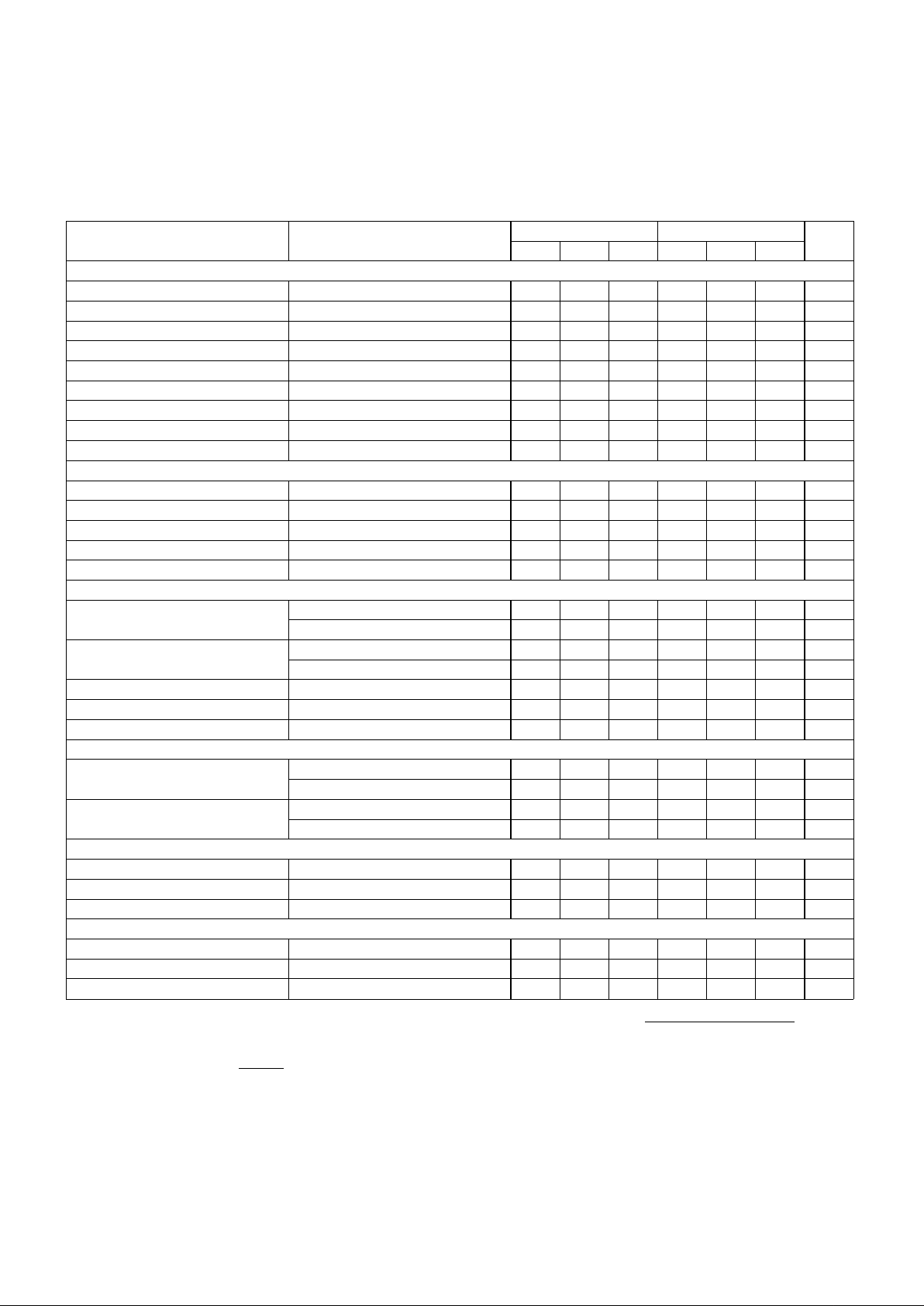
ELECTRICAL CHARACTERISTICS
Unless otherwise stated, these specifications apply for -55°C ≤ TA ≤ 125°C for t h e
UC184xA; -40°C ≤ T
A ≤ 85°C for the UC284xA; 0 ≤ TA ≤ 70°C for the UC384xA; VCC = 15V (Note 5); RT = 10k; CT = 3.3nF; TA = TJ; Pin
numbers refer to DIL-8.
PARAMETER TEST CONDITIONS
UC184xA\UC284xA UC384xA
UNITS
MIN. TYP. MAX. MIN. TYP. MAX.
Reference Sect ion
Output Voltage T
J
= 25°C, IO = 1mA 4.95 5.00 5.05 4.90 5.00 5.10 V
Line Regulation 12 ≤≤ V
IN ≤≤ 25V 6 20 6 20 mV
Load Regulat io n 1 ≤≤ I
O ≤≤ 20mA 6 25 6 25 mV
Temp. Stabilit y (Note 2, Note 7) 0.2 0.4 0.2 0.4 mV/°C
Total Output Variation Line, Load, Temp. 4.9 5.1 4.82 5.18 V
Output Noise Voltage 10Hz ≤≤ f ≤≤ 10kHz
T
J = 25°C (Note 2) 50 50 µV
Long Term Sta bi lity T
A = 125°C, 1000Hrs. (Note 2) 525 525mV
Output Short Circuit -30 -100 -180 -30 -100 -180 mA
Oscillator Section
Initial Accuracy T
J = 25°C (Note 6) 47 52 57 47 52 57 kHz
Voltage Sta b ility 12 ≤≤ V
CC ≤≤ 25V 0.2 1 0.2 1 %
Temp. Stability T
MIN ≤≤ TA ≤≤ TMAX
(Note 2) 5 5 %
Amplitude V
PIN 4 peak to peak (Note 2) 1.7 1.7 V
Discharge Current T
J = 25°C, VPIN 4 = 2V (Note 8) 7.8 8.3 8.8 7.8 8.3 8.8 mA
V
PIN 4 = 2V (Note 8) 7.5 8.8 7.6 8.8 mA
ABSOLUTE MAXIMUM RATINGS (Not e 1)
Note 1. All voltages are with respe ct to Grou nd, Pin 5. Curren ts
are positive into, negative o u t of the spe cified termin al. Co n sult
Packaging Section of Datab ook for therm al limita tion s and co nsiderations of pac kage s. Pin numb ers refer to DIL packa ge only.
PLCC-20, LCC-20
(TOP VIEW)
Q, L Packages
UC1842A/3A/4A/5A
UC2842A/3A/4A/5A
UC3842A/3A/4A/5A
Supply Voltage (Low Imped ance Source) . . . . . . . . . . . . . . 30V
Supply Voltage (I
CC mA). . . . . . . . . . . . . . . . . . . . . Self Limiting
Output Current . . . . . . . . . . . . . . . . . . . . . . . . . . . . . . . . . . . ±1A
Output Energy ( Capac itive Lo ad). . . . . . . . . . . . . . . . . . . . . 5µJ
Analog Inputs (Pins 2, 3) . . . . . . . . . . . . . . . . . . -0.3V to +6.3V
Error Amp Output Sink Curre nt . . . . . . . . . . . . . . . . . . . . 10mA
Power Dissipation at T
A ≤ 25°C (DIL-8). . . . . . . . . . . . . . . . 1W
Storage Tempe rature Rang e . . . . . . . . . . . . . -65°C to +150°C
Lead Temperat ure (Solde ring, 10 Sec onds ) . . . . . . . . . . 300°C
SOIC-14 (TOP VIEW)
D Package
2

PARAMETER TEST CONDITIONS
UC184xA\UC284xA UC384xA
UNITS
MIN. TYP. MAX. MIN. TYP. MAX.
Error Amp Sectio n
Input Voltage V
PIN 1 = 2.5V 2.45 2.50 2.55 2.42 2.50 2.58 V
Input Bias Current -0.3 -1 -0.3 -2 µA
A
VOL 2 ≤ VO ≤ 4V 65 90 65 90 dB
Unity Gain Bandwidth T
J = 25°C (Note 2) 0.7 1 0.7 1 MHz
PSRR 12 ≤ V
CC ≤ 25V 6070 6070 dB
Output Sink Current V
PIN 2 = 2.7V, VPIN 1 = 1.1V 2 6 2 6 mA
Output Source Current V
PIN 2 = 2.3V, VPIN 1 = 5V -0.5 -0.8 -0.5 -0.8 mA
V
OUT High VPIN 2 = 2.3V, RL = 15k to ground 5 6 5 6 V
V
OUT Low VPIN 2 = 2.7V, RL = 15k to Pin 8 0.7 1.1 0.7 1.1 V
Current Sense Section
Gain (Note 3, Note 4) 2.85 3 3.15 2.85 3 3.15 V/V
Maximum Input Signal V
PIN 1 = 5V (Note 3) 0.9 1 1.1 0.9 1 1.1 V
PSRR 12 ≤ V
CC ≤ 25V (Note 3) 70 70 dB
Input Bias Current -2 -10 -2 -10 µA
Dela y to Output V
PIN 3 = 0 to 2V (Note 2) 150 300 150 300 ns
Output Secti on
Output Low Level I
SINK = 20mA 0.1 0.4 0.1 0.4 V
I
SINK = 200mA 15 2.2 15 2.2 V
Output High Level I
SOURCE = 20mA 13 13.5 13 13.5 V
I
SOURCE = 200m A 12 13.5 12 13.5 V
Rise Time T
J = 25°C, CL = 1nF (Note 2) 50 150 50 150 ns
Fall Time T
J = 25°C, CL = 1nF (Note 2) 50 150 50 150 ns
UVLO Saturation V
CC = 5V, ISINK = 10mA 0.7 1.2 0.7 1.2 V
Under-Vol t age Lo ckou t Secti on
Start Threshold x842A/4A 15 16 17 14.5 16 17.5 V
x843A/5A 7.8 8.4 9.0 7.8 8.4 9.0 V
Min. Operat io n Voltage Af te r x842A/4A 9 10 11 8.5 10 11.5 V
Turn On x843A/5A 7.0 7.6 8.2 7.0 7.6 8.2 V
PWM Sectio n
Maximum Duty Cycle x842A/3A 94 96 100 94 96 100 %
x844A/5A 47 48 50 47 48 50 %
Minimum Duty Cycle 0 0 %
Total Standb y Current
Start-Up Cur rent 0.3 0.5 0.3 0.5 mA
Operating Supply Current V
PIN 2 = VPIN 3 = 0V 11 17 11 17 mA
V
CC Zener Voltage ICC = 25mA 30 34 30 34 V
UC1842A/3A/4A/5A
UC2842A/3A/4A/5A
UC3842A/3A/4A/5A
Note 2: These param et ers, alt hou gh gua ran teed, are not 100%
tested in production.
Note 3: Paramete r measu red at trip poin t of latch with V
PIN2
= 0.
Note 4: Gain defined as : A
=
∆
V
PIN 1
∆
V
PIN 3
; 0 ≤ V
PIN 3
≤ 0.8V.
Note 5: Adjust V
CC
above the start thresho ld before setting at
15V .
Note 6: Out put frequency equals oscillator frequency for the
UC1842A and UC1843A. Output frequency is one ha lf
oscillator freque ncy f or the UC1844A and UC1845A.
Note 7: "Temperatu re sta b i lit y, som etimes re fe rr ed to as a ve r ag e
temperature coeffic ient , is describe d by t he equ atio n:
Temp
Stability
=
V
REF
(
max
) −
V
REF
(
min
)
T
J
(
max
) −
T
J
(
min
)
.
V
REF
(max) and V
REF
(min) are the maximum & mini mum reference voltag e me asur ed ov er the ap propriate
temperature range. Note that the extr em es in volt age
do not necessarily occur at the extremes in tempera ture."
Note 8: This paramet er is measure d w ith R
T
= 10kΩ to V
REF
.
This contribut es approximat ely 300
µ
A of current to t h e
measurement. The total current flowing into t he R
T/CT
pin will be approximately 300µA higher than the meas-
ured value.
ELECTRICAL CHARACTERISTICS (cont.) Unless otherwise stated, these specifications apply for -55°C ≤ TA ≤ 125°C for
the UC184xA; -40°C ≤ T
A ≤ 85°C for the UC284xA; 0 ≤ TA ≤ 70°C for the UC384xA; VCC = 15V (Note 5); RT = 10k; CT = 3.3nF; TA = TJ;
Pin numbers re fe r to DIL-8.
3
 Loading...