

TEXAS INSTRUMENTS TMS320F28335, TMS320F28334, TMS320F28332, TMS320F28235, TMS320F28234 Technical data
...
TMS320F28335, TMS320F28334, TMS320F28332
TMS320F28235, TMS320F28234, TMS320F28232
Digital Signal Controllers (DSCs)
Data Manual
June 2007 – Revised February 2008
Literature Number: SPRS439C
ADVANCE INFORMATION concerns new products in the sampling
or preproduction phase of development. Characteristic data and
other specifications are subject to change without notice.

TMS320F28335, TMS320F28334, TMS320F28332
TMS320F28235, TMS320F28234, TMS320F28232
Digital Signal Controllers (DSCs)
SPRS439C – JUNE 2007 – REVISED FEBRUARY 2008
Contents
Revision History .......................................................................................................................... 11
1 TMS320F2833x, TMS320F2823x DSCs ................................................................................... 13
1.1 Features ..................................................................................................................... 13
1.2 Getting Started .............................................................................................................. 14
2 Introduction ....................................................................................................................... 15
2.1 Pin Assignments ............................................................................................................ 17
2.2 Signal Descriptions ......................................................................................................... 26
3 Functional Overview ........................................................................................................... 35
3.1 Memory Maps .............................................................................................................. 36
3.2 Brief Descriptions ........................................................................................................... 42
3.2.1 C28x CPU ....................................................................................................... 42
3.2.2 Memory Bus (Harvard Bus Architecture) .................................................................... 43
3.2.3 Peripheral Bus .................................................................................................. 43
3.2.4 Real-Time JTAG and Analysis ................................................................................ 43
3.2.5 External Interface (XINTF) ..................................................................................... 43
3.2.6 Flash .............................................................................................................. 44
3.2.7 M0, M1 SARAMs ............................................................................................... 44
3.2.8 L0, L1, L2, L3, L4, L5, L6, L7 SARAMs ..................................................................... 44
3.2.9 Boot ROM ........................................................................................................ 44
3.2.10 Security .......................................................................................................... 45
3.2.11 Peripheral Interrupt Expansion (PIE) Block .................................................................. 46
3.2.12 External Interrupts (XINT1-XINT7, XNMI) .................................................................... 47
3.2.13 Oscillator and PLL .............................................................................................. 47
3.2.14 Watchdog ........................................................................................................ 47
3.2.15 Peripheral Clocking ............................................................................................. 47
3.2.16 Low-Power Modes .............................................................................................. 47
3.2.17 Peripheral Frames 0, 1, 2, 3 (PFn) ........................................................................... 47
3.2.18 General-Purpose Input/Output (GPIO) Multiplexer ......................................................... 48
3.2.19 32-Bit CPU-Timers (0, 1, 2) ................................................................................... 48
3.2.20 Control Peripherals ............................................................................................. 48
3.2.21 Serial Port Peripherals ......................................................................................... 48
3.3 Register Map ................................................................................................................ 49
3.4 Device Emulation Registers ............................................................................................... 50
3.5 Interrupts .................................................................................................................... 52
3.5.1 External Interrupts .............................................................................................. 56
3.6 System Control ............................................................................................................. 56
3.6.1 OSC and PLL Block ............................................................................................ 58
3.6.1.1 External Reference Oscillator Clock Option ....................................................... 59
3.6.1.2 PLL-Based Clock Module ............................................................................ 59
3.6.1.3 Loss of Input Clock ................................................................................... 61
3.6.2 Watchdog Block ................................................................................................. 61
3.7 Low-Power Modes Block .................................................................................................. 62
4 Peripherals ........................................................................................................................ 63
4.1 DMA Overview .............................................................................................................. 64
4.2 32-Bit CPU-Timers 0/1/2 .................................................................................................. 65
4.3 Enhanced PWM Modules (ePWM1/2/3/4/5/6) .......................................................................... 67
4.4 High-Resolution PWM (HRPWM) ........................................................................................ 69
4.5 Enhanced CAP Modules (eCAP1/2/3/4/5/6) ............................................................................ 70
4.6 Enhanced QEP Modules (eQEP1/2) ..................................................................................... 72
4.7 Analog-to-Digital Converter (ADC) Module ............................................................................. 74
Contents 2 Submit Documentation Feedback

TMS320F28335, TMS320F28334, TMS320F28332
TMS320F28235, TMS320F28234, TMS320F28232
Digital Signal Controllers (DSCs)
SPRS439C – JUNE 2007 – REVISED FEBRUARY 2008
4.7.1 ADC Connections if the ADC Is Not Used ................................................................... 77
4.7.2 ADC Registers ................................................................................................... 77
4.7.3 ADC Calibration .................................................................................................. 78
4.8 Multichannel Buffered Serial Port (McBSP) Module ................................................................... 79
4.9 Enhanced Controller Area Network (eCAN) Modules (eCAN-A and eCAN-B) ..................................... 82
4.10 Serial Communications Interface (SCI) Modules (SCI-A, SCI-B, SCI-C) ........................................... 87
4.11 Serial Peripheral Interface (SPI) Module (SPI-A) ...................................................................... 91
4.12 Inter-Integrated Circuit (I2C) .............................................................................................. 94
4.13 GPIO MUX .................................................................................................................. 96
4.14 External Interface (XINTF) ............................................................................................... 101
5 Device Support ................................................................................................................. 104
5.1 Device and Development Support Tool Nomenclature .............................................................. 104
5.2 Documentation Support .................................................................................................. 106
6 Electrical Specifications .................................................................................................... 109
6.1 Absolute Maximum Ratings ............................................................................................. 109
6.2 Recommended Operating Conditions .................................................................................. 110
6.3 Electrical Characteristics ................................................................................................ 110
6.4 Current Consumption ..................................................................................................... 111
6.4.1 Reducing Current Consumption ............................................................................. 113
6.4.2 Current Consumption Graphs ................................................................................ 114
6.4.2.1 Thermal Design Considerations .............................................................................. 115
6.5 Emulator Connection Without Signal Buffering for the DSP ........................................................ 115
6.6 Timing Parameter Symbology ........................................................................................... 116
6.6.1 General Notes on Timing Parameters ....................................................................... 116
6.6.2 Test Load Circuit .............................................................................................. 116
6.6.3 Device Clock Table ........................................................................................... 116
6.7 Clock Requirements and Characteristics ............................................................................. 118
6.8 Power Sequencing ........................................................................................................ 119
6.8.1 Power Management and Supervisory Circuit Solutions ................................................... 119
6.9 General-Purpose Input/Output (GPIO) ................................................................................. 122
6.9.1 GPIO - Output Timing ......................................................................................... 122
6.9.2 GPIO - Input Timing ........................................................................................... 123
6.9.3 Sampling Window Width for Input Signals .................................................................. 124
6.9.4 Low-Power Mode Wakeup Timing ........................................................................... 125
6.10 Enhanced Control Peripherals .......................................................................................... 128
6.10.1 Enhanced Pulse Width Modulator (ePWM) Timing ........................................................ 128
6.10.2 Trip-Zone Input Timing ........................................................................................ 128
6.10.3 External Interrupt Timing ...................................................................................... 130
6.10.4 I2C Electrical Specification and Timing ..................................................................... 131
6.10.5 Serial Peripheral Interface (SPI) Master Mode Timing .................................................... 131
6.10.6 SPI Slave Mode Timing ....................................................................................... 135
6.10.7 External Interface (XINTF) Timing ........................................................................... 137
6.10.7.1 USEREADY = 0 .................................................................................... 138
6.10.7.2 Synchronous Mode (USEREADY = 1, READYMODE = 0) .................................. 138
6.10.7.3 Asynchronous Mode (USEREADY = 1, READYMODE = 1) ................................. 139
6.10.7.4 XINTF Signal Alignment to XCLKOUT .......................................................... 140
6.10.7.5 External Interface Read Timing .................................................................. 141
6.10.7.6 External Interface Write Timing .................................................................. 142
6.10.7.7 External Interface Ready-on-Read Timing With One External Wait State ................. 143
6.10.7.8 External Interface Ready-on-Write Timing With One External Wait State ................. 147
6.10.8 XHOLD and XHOLDA Timing ................................................................................ 149
6.10.9 On-Chip Analog-to-Digital Converter ........................................................................ 152
Contents 3

TMS320F28335, TMS320F28334, TMS320F28332
TMS320F28235, TMS320F28234, TMS320F28232
Digital Signal Controllers (DSCs)
SPRS439C – JUNE 2007 – REVISED FEBRUARY 2008
6.10.9.1 ADC Power-Up Control Bit Timing .............................................................. 153
6.10.9.2 Definitions ........................................................................................... 154
6.10.9.3 Sequential Sampling Mode (Single-Channel) (SMODE = 0) ................................. 155
6.10.9.4 Simultaneous Sampling Mode (Dual-Channel) (SMODE = 1) ............................... 156
6.10.10 Detailed Descriptions ........................................................................................ 157
6.10.11 Multichannel Buffered Serial Port (McBSP) Timing ....................................................... 158
6.10.11.0.1 McBSP Transmit and Receive Timing ...................................................... 158
6.10.11.0.2 McBSP as SPI Master or Slave Timing ..................................................... 160
6.11 Migrating From F2833x Devices to F2823x Devices ................................................................. 163
7 Thermal/Mechanical Data ................................................................................................... 164
Contents 4 Submit Documentation Feedback

TMS320F28335, TMS320F28334, TMS320F28332
TMS320F28235, TMS320F28234, TMS320F28232
Digital Signal Controllers (DSCs)
SPRS439C – JUNE 2007 – REVISED FEBRUARY 2008
List of Figures
2-1 F2833x, F2823x 176-Pin PGF LQFP (Top View) ............................................................................. 17
2-2 F2833x, F2823x 179-Ball ZHH MicroStar BGA™ (Upper Left Quadrant) (Bottom View) ............................... 18
2-3 F2833x, F2823x 179-Ball ZHH MicroStar BGA™ (Upper Right Quadrant) (Bottom View) .............................. 19
2-4 F2833x, F2823x 179-Ball ZHH MicroStar BGA™ (Lower Left Quadrant) (Bottom View) ............................... 20
2-5 F2833x, F2823x 179-Ball ZHH MicroStar BGA ™(Lower Right Quadrant) (Bottom View) .............................. 21
2-6 F2833x, F2823x 176-Ball ZJZ Plastic BGA (Upper Left Quadrant) (Bottom View) ...................................... 22
2-7 F2833x, F2823x 176-Ball ZJZ Plastic BGA (Upper Right Quadrant) (Bottom View) ..................................... 23
2-8 F2833x, F2823x 176-Ball ZJZ Plastic BGA (Lower Left Quadrant) (Bottom View) ...................................... 24
2-9 F2833x, F2823x 176-Ball ZJZ Plastic BGA (Lower Right Quadrant) (Bottom View) ..................................... 25
3-1 Functional Block Diagram ....................................................................................................... 35
3-2 F28335/F28235 Memory Map ................................................................................................... 37
3-3 F28334/F28234 Memory Map ................................................................................................... 38
3-4 F28332/F28232 Memory Map ................................................................................................... 39
3-5 External and PIE Interrupt Sources ............................................................................................. 52
3-6 External Interrupts ................................................................................................................ 53
3-7 Multiplexing of Interrupts Using the PIE Block ................................................................................ 54
3-8 Clock and Reset Domains ....................................................................................................... 57
3-9 OSC and PLL Block Diagram ................................................................................................... 58
3-10 Using a 3.3-V External Oscillator ............................................................................................... 59
3-11 Using a 1.9-V External Oscillator ............................................................................................... 59
3-12 Using the Internal Oscillator ..................................................................................................... 59
3-13 Watchdog Module ................................................................................................................. 61
4-1 DMA Functional Block Diagram ................................................................................................. 64
4-2 CPU-Timers ........................................................................................................................ 65
4-3 CPU-Timer Interrupt Signals and Output Signal .............................................................................. 65
4-4 Multiple PWM Modules in a F2833x/F2823x System ........................................................................ 67
4-5 ePWM Sub-Modules Showing Critical Internal Signal Interconnections ................................................... 69
4-6 eCAP Functional Block Diagram ................................................................................................ 70
4-7 eQEP Functional Block Diagram ................................................................................................ 72
4-8 Block Diagram of the ADC Module ............................................................................................. 75
4-9 ADC Pin Connections With Internal Reference ............................................................................... 76
4-10 ADC Pin Connections With External Reference .............................................................................. 76
4-11 McBSP Module ................................................................................................................... 80
4-12 eCAN Block Diagram and Interface Circuit .................................................................................... 83
4-13 eCAN-A Memory Map ............................................................................................................ 84
4-14 eCAN-B Memory Map ............................................................................................................ 85
4-15 Serial Communications Interface (SCI) Module Block Diagram ............................................................ 90
4-16 SPI Module Block Diagram (Slave Mode) ..................................................................................... 93
4-17 I2C Peripheral Module Interfaces ............................................................................................... 95
List of Figures 5

TMS320F28335, TMS320F28334, TMS320F28332
TMS320F28235, TMS320F28234, TMS320F28232
Digital Signal Controllers (DSCs)
SPRS439C – JUNE 2007 – REVISED FEBRUARY 2008
4-18 GPIO MUX Block Diagram ....................................................................................................... 96
4-19 Qualification Using Sampling Window ........................................................................................ 101
4-20 External Interface Block Diagram ............................................................................................. 102
4-21 Typical 16-bit Data Bus XINTF Connections ................................................................................. 102
4-22 Typical 32-bit Data Bus XINTF Connections ................................................................................. 103
5-1 Example of F2833x, F2823x Device Nomenclature ......................................................................... 105
6-1 Typical Operational Current Versus Frequency (F28335/F28235/F28334/F28234) .................................... 114
6-2 Typical Operational Power Versus Frequency (F28335/F28235/F28334/F28234) ..................................... 114
6-3 Emulator Connection Without Signal Buffering for the DSP ............................................................... 115
6-4 3.3-V Test Load Circuit ......................................................................................................... 116
6-5 Clock Timing ..................................................................................................................... 119
6-6 Power-on Reset .................................................................................................................. 120
6-7 Warm Reset ...................................................................................................................... 121
6-8 Example of Effect of Writing Into PLLCR Register .......................................................................... 122
6-9 General-Purpose Output Timing ............................................................................................... 122
6-10 Sampling Mode .................................................................................................................. 123
6-11 General-Purpose Input Timing ................................................................................................. 124
6-12 IDLE Entry and Exit Timing .................................................................................................... 125
6-13 STANDBY Entry and Exit Timing Diagram ................................................................................... 126
6-14 HALT Wake-Up Using GPIOn ................................................................................................. 127
6-15 PWM Hi-Z Characteristics ...................................................................................................... 128
6-16 ADCSOCAO or ADCSOCBO Timing ......................................................................................... 130
6-17 External Interrupt Timing ....................................................................................................... 130
6-18 SPI Master Mode External Timing (Clock Phase = 0) ...................................................................... 133
6-19 SPI Master Mode External Timing (Clock Phase = 1) ...................................................................... 135
6-20 SPI Slave Mode External Timing (Clock Phase = 0) ........................................................................ 136
6-21 SPI Slave Mode External Timing (Clock Phase = 1) ........................................................................ 137
6-22 Relationship Between XTIMCLK and SYSCLKOUT ........................................................................ 140
6-23 Example Read Access .......................................................................................................... 142
6-24 Example Write Access .......................................................................................................... 143
6-25 Example Read With Synchronous XREADY Access ....................................................................... 145
6-26 Example Read With Asynchronous XREADY Access ...................................................................... 146
6-27 Write With Synchronous XREADY Access ................................................................................... 148
6-28 Write With Asynchronous XREADY Access ................................................................................. 149
6-29 External Interface Hold Waveform ............................................................................................ 150
6-30 XHOLD/ XHOLDA Timing Requirements (XCLKOUT = 1/2 XTIMCLK) ................................................... 151
6-31 ADC Power-Up Control Bit Timing ............................................................................................ 153
6-32 ADC Analog Input Impedance Model ......................................................................................... 154
6-33 Sequential Sampling Mode (Single-Channel) Timing ....................................................................... 155
6-34 Simultaneous Sampling Mode Timing ........................................................................................ 156
6-35 McBSP Receive Timing ......................................................................................................... 159
List of Figures6 Submit Documentation Feedback

TMS320F28335, TMS320F28334, TMS320F28332
TMS320F28235, TMS320F28234, TMS320F28232
Digital Signal Controllers (DSCs)
SPRS439C – JUNE 2007 – REVISED FEBRUARY 2008
6-36 McBSP Transmit Timing ........................................................................................................ 160
6-37 McBSP Timing as SPI Master or Slave: CLKSTP = 10b, CLKXP = 0 .................................................... 161
6-38 McBSP Timing as SPI Master or Slave: CLKSTP = 11b, CLKXP = 0 .................................................... 161
6-39 McBSP Timing as SPI Master or Slave: CLKSTP = 10b, CLKXP = 1 .................................................... 162
6-40 McBSP Timing as SPI Master or Slave: CLKSTP = 11b, CLKXP = 1 .................................................... 163
List of Figures 7

TMS320F28335, TMS320F28334, TMS320F28332
TMS320F28235, TMS320F28234, TMS320F28232
Digital Signal Controllers (DSCs)
SPRS439C – JUNE 2007 – REVISED FEBRUARY 2008
List of Tables
2-1 F2833x Hardware Features ..................................................................................................... 15
2-2 F2823x Hardware Features ..................................................................................................... 16
2-3 Signal Descriptions ............................................................................................................... 26
3-1 Addresses of Flash Sectors in F28335/F28235 .............................................................................. 40
3-2 Addresses of Flash Sectors in F28334/F28234 ............................................................................... 40
3-3 Addresses of Flash Sectors in F28332/F28232 ............................................................................... 40
3-4 Handling Security Code Locations .............................................................................................. 41
3-5 Wait-states ......................................................................................................................... 42
3-6 Boot Mode Selection .............................................................................................................. 45
3-7 Peripheral Frame 0 Registers .................................................................................................. 49
3-8 Peripheral Frame 1 Registers ................................................................................................... 50
3-9 Peripheral Frame 2 Registers ................................................................................................... 50
3-10 Peripheral Frame 3 Registers ................................................................................................... 50
3-11 Device Emulation Registers ..................................................................................................... 51
3-12 PIE Peripheral Interrupts ........................................................................................................ 54
3-13 PIE Configuration and Control Registers ...................................................................................... 55
3-14 External Interrupt Registers ...................................................................................................... 56
3-15 PLL, Clocking, Watchdog, and Low-Power Mode Registers ................................................................ 58
3-16 PLLCR Bit Descriptions .......................................................................................................... 60
3-17 CLKIN Divide Options ............................................................................................................ 60
3-18 Possible PLL Configuration Modes ............................................................................................. 60
3-19 Low-Power Modes ................................................................................................................ 62
4-1 CPU-Timers 0, 1, 2 Configuration and Control Registers ................................................................... 66
4-2 ePWM Control and Status Registers ........................................................................................... 68
4-3 eCAP Control and Status Registers ............................................................................................ 71
4-4 eQEP Control and Status Registers ............................................................................................ 73
4-5 ADC Registers ..................................................................................................................... 77
4-6 McBSP Register Summary ...................................................................................................... 81
4-7 3.3-V eCAN Transceivers ....................................................................................................... 83
4-8 CAN Register Map ............................................................................................................... 86
4-9 SCI-A Registers .................................................................................................................. 88
4-10 SCI-B Registers .................................................................................................................. 88
4-11 SCI-C Registers .................................................................................................................. 89
4-12 SPI-A Registers ................................................................................................................... 92
4-13 I2C-A Registers .................................................................................................................... 95
4-14 GPIO Registers ................................................................................................................... 97
4-15 GPIO-A Mux Peripheral Selection Matrix ..................................................................................... 98
4-16 GPIO-B Mux Peripheral Selection Matrix ..................................................................................... 99
4-17 GPIO-C Mux Peripheral Selection Matrix .................................................................................... 100
List of Tables8 Submit Documentation Feedback

TMS320F28335, TMS320F28334, TMS320F28332
TMS320F28235, TMS320F28234, TMS320F28232
Digital Signal Controllers (DSCs)
SPRS439C – JUNE 2007 – REVISED FEBRUARY 2008
4-18 XINTF Configuration and Control Register Mapping ........................................................................ 103
6-1 TMS320F28335/F28235 Current Consumption by Power-Supply Pins at 150-MHz SYSCLKOUT .................. 111
6-2 TMS320F28334/F28234 Current Consumption by Power-Supply Pins at 150-MHz SYSCLKOUT .................. 112
6-3 Typical Current Consumption by Various Peripherals (at 150 MHz) ..................................................... 113
6-4 Clocking and Nomenclature (150-MHz devices) ............................................................................ 117
6-5 Clocking and Nomenclature (100-MHz devices) ............................................................................ 117
6-6 Input Clock Frequency .......................................................................................................... 118
6-7 XCLKIN Timing Requirements - PLL Enabled ............................................................................... 118
6-8 XCLKIN Timing Requirements - PLL Disabled .............................................................................. 118
6-9 XCLKOUT Switching Characteristics (PLL Bypassed or Enabled) ....................................................... 118
6-10 Power Management and Supervisory Circuit Solutions .................................................................... 119
6-11 Reset ( XRS) Timing Requirements ........................................................................................... 121
6-12 General-Purpose Output Switching Characteristics ......................................................................... 122
6-13 General-Purpose Input Timing Requirements ............................................................................... 123
6-14 IDLE Mode Timing Requirements ............................................................................................. 125
6-15 IDLE Mode Switching Characteristics ......................................................................................... 125
6-16 STANDBY Mode Timing Requirements ...................................................................................... 125
6-17 STANDBY Mode Switching Characteristics ................................................................................. 126
6-18 HALT Mode Timing Requirements ............................................................................................ 126
6-19 HALT Mode Switching Characteristics ....................................................................................... 127
6-20 ePWM Timing Requirements................................................................................................... 128
6-21 ePWM Switching Characteristics .............................................................................................. 128
6-22 Trip-Zone input Timing Requirements ........................................................................................ 128
6-23 High Resolution PWM Characteristics at SYSCLKOUT = (60 - 150 MHz) .............................................. 129
6-24 Enhanced Capture (eCAP) Timing Requirement ............................................................................ 129
6-25 eCAP Switching Characteristics ............................................................................................... 129
6-26 Enhanced Quadrature Encoder Pulse (eQEP) Timing Requirements .................................................... 129
6-27 eQEP Switching Characteristics ............................................................................................... 129
6-28 External ADC Start-of-Conversion Switching Characteristics .............................................................. 129
6-29 External Interrupt Timing Requirements ...................................................................................... 130
6-30 External Interrupt Switching Characteristics ................................................................................. 130
6-31 I2C Timing ....................................................................................................................... 131
6-32 SPI Master Mode External Timing (Clock Phase = 0) ...................................................................... 132
6-33 SPI Master Mode External Timing (Clock Phase = 1) ...................................................................... 134
6-34 SPI Slave Mode External Timing (Clock Phase = 0)........................................................................ 135
6-35 SPI Slave Mode External Timing (Clock Phase = 1)........................................................................ 136
6-36 Relationship Between Parameters Configured in XTIMING and Duration of Pulse .................................... 137
6-37 XINTF Clock Configurations .................................................................................................... 139
6-38 External Interface Read Timing Requirements .............................................................................. 141
6-39 External Interface Read Switching Characteristics .......................................................................... 141
6-40 External Interface Write Switching Characteristics .......................................................................... 142
List of Tables 9

TMS320F28335, TMS320F28334, TMS320F28332
TMS320F28235, TMS320F28234, TMS320F28232
Digital Signal Controllers (DSCs)
SPRS439C – JUNE 2007 – REVISED FEBRUARY 2008
6-41 External Interface Read Switching Characteristics (Ready-on-Read, 1 Wait State) .................................... 143
6-42 External Interface Read Timing Requirements (Ready-on-Read, 1 Wait State) ........................................ 143
6-43 Synchronous XREADY Timing Requirements (Ready-on-Read, 1 Wait State) ......................................... 144
6-44 Asynchronous XREADY Timing Requirements (Ready-on-Read, 1 Wait State) ........................................ 144
6-45 External Interface Write Switching Characteristics (Ready-on-Write, 1 Wait State) .................................... 147
6-46 Synchronous XREADY Timing Requirements (Ready-on-Write, 1 Wait State) ......................................... 147
6-47 Asynchronous XREADY Timing Requirements (Ready-on-Write, 1 Wait State) ........................................ 147
6-48 XHOLD/ XHOLDA Timing Requirements (XCLKOUT = XTIMCLK) ....................................................... 150
6-49 XHOLD/ XHOLDA Timing Requirements (XCLKOUT = 1/2 XTIMCLK) ................................................... 151
6-50 ADC Electrical Characteristics (over recommended operating conditions) .............................................. 152
6-51 ADC Power-Up Delays .......................................................................................................... 153
6-52 Current Consumption for Different ADC Configurations (at 25-MHz ADCCLK) ......................................... 153
6-53 Sequential Sampling Mode Timing ............................................................................................ 155
6-54 Simultaneous Sampling Mode Timing ........................................................................................ 156
6-55 McBSP Timing Requirements .................................................................................................. 158
6-56 McBSP Switching Characteristics ............................................................................................. 158
6-57 McBSP as SPI Master or Slave Timing Requirements (CLKSTP = 10b, CLKXP = 0) ................................. 160
6-58 McBSP as SPI Master or Slave Switching Characteristics (CLKSTP = 10b, CLKXP = 0) ............................. 160
6-59 McBSP as SPI Master or Slave Timing Requirements (CLKSTP = 11b, CLKXP = 0) ................................. 161
6-60 McBSP as SPI Master or Slave Switching Characteristics (CLKSTP = 11b, CLKXP = 0) ............................. 161
6-61 McBSP as SPI Master or Slave Timing Requirements (CLKSTP = 10b, CLKXP = 1) ................................. 162
6-62 McBSP as SPI Master or Slave Switching Characteristics (CLKSTP = 10b, CLKXP = 1) ............................. 162
6-63 McBSP as SPI Master or Slave Timing Requirements (CLKSTP = 11b, CLKXP = 1) ................................. 162
6-64 McBSP as SPI Master or Slave Switching Characteristics (CLKSTP = 11b, CLKXP = 1) ............................. 163
7-1 Thermal Model 176-pin PGF Results ......................................................................................... 164
7-2 Thermal Model 179-pin ZHH Results ......................................................................................... 164
7-3 Thermal Model 176-pin ZJZ Results ......................................................................................... 164
List of Tables10 Submit Documentation Feedback

TMS320F28335, TMS320F28334, TMS320F28332
TMS320F28235, TMS320F28234, TMS320F28232
Revision History
NOTE: Page numbers for previous revisions may differ from page numbers in the current version.
The table lists the technical changes made for this revision.
Changes Made in Revision C
Location Additions, Deletions, Modifications
Global Added TMS320F28235, TMS320F28234, and TMS320F28232 devices.
Table 2-2 Added F2823x hardware features table.
Figure 3-1 Modified the functional block diagram.
Section 3.1 Changed the fifth bullet under memory maps section.
Figure 3-2 – Figure 3-4 Modified all three memory maps.
Section 3.2.19 Deleted a sentence in section on 32-Bit CPU Timers (0, 1, 2).
Section 3.6.1.2 Added a sentence to the section on PLL-Based Clock Module.
Figure 3-8 Modified the Clock and Reset Diagram.
Figure 4-9 and
Figure 4-10
Figure 4-11 Modified the McBSP block diagram.
Figure 5-1 Modified the Device Nomenclature figure to include new devices.
Table 6-1 and Table 6-2 Modified current consumption tables by adding a seventh note.
Table 6-3 Modified Typical Current Consumption table by adding a fourth note.
Table 6-50 Modified ADC Electrical Characteristics table by deleting a row.
Section 6.11 Added section on migrating from F2833x to F2823x devices
Modified the ADC Pin Connection Figures.
Digital Signal Controllers (DSCs)
SPRS439C – JUNE 2007 – REVISED FEBRUARY 2008
Revision History 11

TMS320F28335, TMS320F28334, TMS320F28332
TMS320F28235, TMS320F28234, TMS320F28232
Digital Signal Controllers (DSCs)
SPRS439C – JUNE 2007 – REVISED FEBRUARY 2008
Revision History12 Submit Documentation Feedback

www.ti.com
ADVANCE INFORMATION
TMS320F28335, TMS320F28334, TMS320F28332
TMS320F28235, TMS320F28234, TMS320F28232
1 TMS320F2833x, TMS320F2823x DSCs
1.1 Features
• High-Performance Static CMOS Technology
– Up to 150 MHz (6.67-ns Cycle Time)
– 1.9-V Core, 3.3-V I/O Design
• High-Performance 32-Bit CPU (TMS320C28x)
– IEEE-754 Single-Precision Floating-Point
Unit (FPU) (2833x only)
– 16 x 16 and 32 x 32 MAC Operations
– 16 x 16 Dual MAC
– Harvard Bus Architecture
– Fast Interrupt Response and Processing
– Unified Memory Programming Model
– Code-Efficient (in C/C++ and Assembly)
• Six Channel DMA Controller (for ADC, McBSP,
XINTF, and SARAM) – 2 x 8 Channel Input Multiplexer
• 16-bit or 32-bit External Interface (XINTF)
– Over 2M x 16 Address Reach
• On-Chip Memory
– F28335/F28235: 256K x 16 Flash, 34K x 16
SARAM
– F28334/F28234: 128K x 16 Flash, 34K x 16
SARAM
– F28332/F28232: 64K x 16 Flash, 26K x 16
SARAM
– 1K x 16 OTP ROM
• Boot ROM (8K x 16)
– With Software Boot Modes (via SCI, SPI,
CAN, I2C, McBSP, XINTF, and Parallel I/O)
– Standard Math Tables
• Clock and System Control
– Dynamic PLL Ratio Changes Supported
– On-Chip Oscillator
– Watchdog Timer Module
• GPIO0 to GPIO63 Pins Can Be Connected to
One of the Eight External Core Interrupts
• Peripheral Interrupt Expansion (PIE) Block
That Supports All 58 Peripheral Interrupts
• 128-Bit Security Key/Lock
– Protects Flash/OTP/RAM Blocks
– Prevents Firmware Reverse Engineering
• Enhanced Control Peripherals
– Up to 18 PWM Outputs
– Up to 6 HRPWM Outputs With 150 ps MEP
Resolution
– Up to 6 Event Capture Inputs
– Up to 2 Quadrature Encoder Interfaces
– Up to 8 32-bit/Six 16-bit Timers
• Three 32-Bit CPU Timers
• Serial Port Peripherals
– Up to 2 CAN Modules
– Up to 3 SCI (UART) Modules
– Up to 2 McBSP Modules (Configurable as
SPI)
– One SPI Module
– One Inter-Integrated-Circuit (I2C) Bus
• 12-Bit ADC, 16 Channels
– 80-ns Conversion Rate
– Two Sample-and-Hold
– Single/Simultaneous Conversions
– Internal or External Reference
• Up to 88 Individually Programmable,
Multiplexed GPIO Pins With Input Filtering
• JTAG Boundary Scan Support
• Advanced Emulation Features
– Analysis and Breakpoint Functions
– Real-Time Debug via Hardware
• Development Support Includes
– ANSI C/C++ Compiler/Assembler/Linker
– Code Composer Studio™ IDE
– DSP/BIOS™
– Digital Motor Control and Digital Power
Software Libraries
• Low-Power Modes and Power Savings
– IDLE, STANDBY, HALT Modes Supported
– Disable Individual Peripheral Clocks
• Package Options
– Lead-free Green Packaging
– Thin Quad Flatpack (PGF)
– MicroStar BGA™ (ZHH)
– Plastic BGA (ZJZ)
• Temperature Options:
– A: –40 ° C to 85 ° C (PGF, ZHH, ZJZ)
– S: –40 ° C to 125 ° C (ZJZ)
(1) IEEE Standard 1149.1-1990 Standard Test Access Port and
Boundary Scan Architecture
Digital Signal Controllers (DSCs)
SPRS439C – JUNE 2007 – REVISED FEBRUARY 2008
(1)
Please be aware that an important notice concerning availability, standard warranty, and use in critical applications of Texas
Instruments semiconductor products and disclaimers thereto appears at the end of this document.
Code Composer Studio, DSP/BIOS, MicroStar BGA, TMS320C28x, TMS320C54x, TMS320C55x, C28x are trademarks of Texas
Instruments.
ADVANCE INFORMATION concerns new products in the sampling
or preproduction phase of development. Characteristic data and
other specifications are subject to change without notice.
Copyright © 2007–2008, Texas Instruments Incorporated

www.ti.com
ADVANCE INFORMATION
TMS320F28335, TMS320F28334, TMS320F28332
TMS320F28235, TMS320F28234, TMS320F28232
Digital Signal Controllers (DSCs)
SPRS439C – JUNE 2007 – REVISED FEBRUARY 2008
1.2 Getting Started
This section gives a brief overview of the steps to take when first developing for a C28x device. For more
detail on each of these steps, see the following:
• Getting Started With TMS320C28x™ Digital Signal Controllers (literature number SPRAAM0 ).
• C2000 Getting Started Website (http://www.ti.com/c2000getstarted)
14 TMS320F2833x, TMS320F2823x DSCs Submit Documentation Feedback
www.ti.com
ADVANCE INFORMATION
TMS320F28335, TMS320F28334, TMS320F28332
TMS320F28235, TMS320F28234, TMS320F28232
Digital Signal Controllers (DSCs)
SPRS439C – JUNE 2007 – REVISED FEBRUARY 2008
2 Introduction
The TMS320F28335, TMS320F28334, TMS320F28332, TMS320F28235, TMS320F28234, and
TMS320F28232 devices, members of the TMS320C28x™ DSC generation, are highly integrated,
high-performance solutions for demanding control applications.
Throughout this document, the devices are abbreviated as F28335, F28334, F28332, F28235, F28234,
and F28232, respectively. Table 2-1 and Table 2-2 provide a summary of features for each device.
Table 2-1. F2833x Hardware Features
FEATURE F28335 (150 MHz) F28334 (150 MHz) F28332 (100 MHz)
Instruction cycle 6.67 ns 6.67 ns 10 ns
Floating-point Unit Yes Yes Yes
3.3-V on-chip flash (16-bit word) 256K 128K 64K
Single-access RAM (SARAM) (16-bit word) 34K 34K 26K
One-time programmable (OTP) ROM
(16-bit word)
Code security for on-chip flash/SARAM/OTP
blocks
Boot ROM (8K X16) Yes Yes Yes
16/32-bit External Interface (XINTF) Yes Yes Yes
6-channel Direct Memory Access (DMA) Yes Yes Yes
PWM outputs ePWM1/2/3/4/5/6 ePWM1/2/3/4/5/6 ePWM1/2/3/4/5/6
HRPWM channels ePWM1A/2A/3A/4A/5A/6A ePWM1A/2A/3A/4A/5A/6A ePWM1A/2A/3A/4A
32-bit Capture inputs or auxiliary PWM outputs 6 6 4
32-bit QEP channels (four inputs/channel) 2 2 2
Watchdog timer Yes Yes Yes
No. of channels 16 16 16
12-Bit ADC MSPS 12.5 12.5 12.5
Conversion time 80 ns 80 ns 80 ns
32-Bit CPU timers 3 3 3
Multichannel Buffered Serial Port (McBSP)/SPI 2 2 1
Serial Peripheral Interface (SPI) 1 1 1
Serial Communications Interface (SCI) 3 3 2
Enhanced Controller Area Network (eCAN) 2 2 2
Inter-Integrated Circuit (I2C) 1 1 1
General Purpose I/O pins (shared) 88 88 88
External interrupts 8 8 8
176-Pin PGF Yes Yes Yes
Packaging 179-Ball ZHH Yes Yes Yes
176-Ball ZJZ Yes Yes Yes
Temperature options
Product status TMX TMX TMX
A: –40 ° C to 85 ° C (PGF, ZHH, ZJZ) (PGF, ZHH, ZJZ) (PGF, ZHH, ZJZ)
S: –40 ° C to 125 ° C (ZJZ) (ZJZ) (ZJZ)
1K 1K 1K
Yes Yes Yes
Submit Documentation Feedback Introduction 15
www.ti.com
ADVANCE INFORMATION
TMS320F28335, TMS320F28334, TMS320F28332
TMS320F28235, TMS320F28234, TMS320F28232
Digital Signal Controllers (DSCs)
SPRS439C – JUNE 2007 – REVISED FEBRUARY 2008
Table 2-2. F2823x Hardware Features
FEATURE F28235 (150 MHz) F28234 (150 MHz) F28232 (100 MHz)
Instruction cycle 6.67 ns 6.67 ns 10 ns
Floating-point Unit No No No
3.3-V on-chip flash (16-bit word) 256K 128K 64K
Single-access RAM (SARAM) (16-bit word) 34K 34K 26K
One-time programmable (OTP) ROM
(16-bit word)
Code security for on-chip flash/SARAM/OTP
blocks
Boot ROM (8K X16) Yes Yes Yes
16/32-bit External Interface (XINTF) Yes Yes Yes
6-channel Direct Memory Access (DMA) Yes Yes Yes
PWM outputs ePWM1/2/3/4/5/6 ePWM1/2/3/4/5/6 ePWM1/2/3/4/5/6
HRPWM channels ePWM1A/2A/3A/4A/5A/6A ePWM1A/2A/3A/4A/5A/6A ePWM1A/2A/3A/4A
32-bit Capture inputs or auxiliary PWM outputs 6 6 4
32-bit QEP channels (four inputs/channel) 2 2 2
Watchdog timer Yes Yes Yes
No. of channels 16 16 16
12-Bit ADC MSPS 12.5 12.5 12.5
Conversion time 80 ns 80 ns 80 ns
32-Bit CPU timers 3 3 3
Multichannel Buffered Serial Port (McBSP)/SPI 2 2 1
Serial Peripheral Interface (SPI) 1 1 1
Serial Communications Interface (SCI) 3 3 2
Enhanced Controller Area Network (eCAN) 2 2 2
Inter-Integrated Circuit (I2C) 1 1 1
General Purpose I/O pins (shared) 88 88 88
External interrupts 8 8 8
176-Pin PGF Yes Yes Yes
Packaging 179-Ball ZHH Yes Yes Yes
176-Ball ZJZ Yes Yes Yes
Temperature options
Product status
(1) See Section 5.1, Device and Development Support Nomenclature for descriptions of device stages.
(1)
A: –40 ° C to 85 ° C (PGF, ZHH, ZJZ) (PGF, ZHH, ZJZ) (PGF, ZHH, ZJZ)
S: –40 ° C to 125 ° C (ZJZ) (ZJZ) (ZJZ)
1K 1K 1K
Yes Yes Yes
TMX TMX TMX
Introduction 16 Submit Documentation Feedback
www.ti.com
ADVANCE INFORMATION
88
87
86
85
84
83
82
81
80
79
78
77
76
75
74
73
72
71
70
69
68
67
66
65
64
63
62
61
60
59
58
57
56
55
54
53
52
51
50
49
48
47
46
45
133
134
135
136
137
138
139
140
141
142
143
144
145
146
147
148
149
150
151
152
153
154
155
156
157
158
159
160
161
162
163
164
165
166
167
168
169
170
171
172
173
174
175
176
1
2
3
4
5
6
7
8
9
10
11
12
13
14
15
16
17
18
19
20
21
22
23
24
25
26
27
28
29
30
31
32
33
34
35
36
37
38
39
40
41
42
43
44
132
131
130
129
128
127
126
125
124
123
122
121
120
119
118
117
116
1
15
114
113
112
11
1
110
109
108
107
106
105
104
103
102
101
100
99
98
97
96
95
94
93
92
91
90
89
GPIO48/ECAP5/XD31
TCK
EMU1
EMU0
V
DD3VFL
V
SS
TEST2
TEST1
XRS
TMS
TRST
TDO
TDI
GPIO33/SCLA/EPWMSYNCO/ADCSOCBO
GPIO32/SDAA/EPWMSYNCI/ADCSOCAO
GPIO27/ECAP4/EQEP2S/MFSXB
GPIO26/ECAP3/EQEP2I/MCLKXB
V
DDIO
V
SS
GPIO25/ECAP2/EQEP2B/MDRB
GPIO24/ECAP1/EQEP2A/MDXB
GPIO23/EQEP1I/MFSXA/SCIRXDB
GPIO22/EQEP1S/MCLKXA/SCITXDB
GPIO21/EQEP1B/MDRA/CANRXB
GPIO20/EQEP1A/MDXA/CANTXB
GPIO19/ /SCIRXDB/CANTXASPISTEA
GPIO18/SPICLKA/SCITXDB/CANRXA
V
DD
V
SS
V
DD2A18
V
SS2AGND
ADCRESEXT
ADCREFP
ADCREFM
ADCREFIN
ADCINB7
ADCINB6
ADCINB5
ADCINB4
ADCINB3
ADCINB2
ADCINB1
ADCINB0
V
DDAIO
GPIO75/XD4
GPIO74/XD5
GPIO73/XD6
GPIO72/XD7
GPIO71/XD8
GPIO70/XD9
V
DDVSS
GPIO69/XD10
GPIO68/XD11
GPIO67/XD12
V
DDIOVSS
GPIO66/XD13
V
SSVDD
GPIO65/XD14
GPIO64/XD15
GPIO63/SCITXDC/XD16
GPIO62/SCIRXDC/XD17
GPIO61/MFSRB/XD18
GPIO60/MCLKRB/XD19
GPIO59/MFSRA/XD20
V
DDVSSVDDIOVSS
XCLKIN
X1
V
SS
X2
V
DD
GPIO58/MCLKRA/XD21
GPIO57/ /XD22SPISTEA
GPIO56/SPICLKA/XD23
GPIO55/SPISOMIA/XD24
GPIO54/SPISIMOA/XD25
GPIO53/EQEP1I/XD26
GPIO52/EQEP1S/XD27
V
DDIOVSS
GPIO51/EQEP1B/XD28
GPIO50/EQEP1A/XD29
GPIO49/ECAP6/XD30
GPIO30/CANRXA/XA18
GPIO29/SCITXDA/XA19
V
SS
V
DD
GPIO0/EPWM1A
GPIO1/EPWM1B/ECAP6/MFSRB
GPIO2/EPWM2A
V
SS
V
DDIO
GPIO3/EPWM2B/ECAP5/MCLKRB
GPIO4/EPWM3A
GPIO5/EPWM3B/MFSRA/ECAP1
GPIO6/EPWM4A/EPWMSYNCI/EPWMSYNCO
V
SS
V
DD
GPIO7/EPWM4B/MCLKRA/ECAP2
GPIO8/EPWM5A/CANTXB/
ADCSOCAO
GPIO9/EPWM5B/SCITXDB/ECAP3
GPIO10/EPWM6A/CANRXB/
ADCSOCBO
GPIO1
1/EPWM6B/SCIRXDB/ECAP4
GPIO12 /CANTXB/MDXB/TZ1
V
SS
V
DD
GPIO13/ /CANRXB/MDRBTZ2
GPIO14/ /XHOLD/ /
TZ3 SCITXDBMCLKXB
GPIO15/ /XHOLDATZ4 /SCIRXDB/MFSXB
GPIO16/SPISIMOA/CANTXB/TZ5
GPIO17/SPISOMIA/CANRXB/TZ6
V
D
D
V
SS
V
DD1A18
V
SS1AGND
V
SSA2
V
DDA2
ADCINA7
ADCINA6
ADCINA5
ADCINA4
ADCINA3
ADCINA2
ADCINA1
ADCINA0
ADCLO
V
SSAIO
GPIO76/XD3
GPIO77/XD2
GPIO78/XD1
GPIO79/XD0
GPIO38/XWE0
XCLKOUT
V
DD
V
SS
GPIO28/SCIRXDA/XZCS6
GPIO34/ECAP1/XREADY
V
DDIO
V
SS
GPIO36/SCIRXDA/XZCS0
V
DD
V
SS
GPIO35/SCITXDA/XR/W
XRD
GPIO37/ECAP2/XZCS7
GPIO40/XA0/XWE1
GPIO41/XA1
GPIO42/XA2
V
DD
V
SS
GPIO43/XA3
GPIO44/XA4
GPIO45/XA5
V
DDIO
V
SS
GPIO46/XA6
GPIO47/XA7
GPIO80/XA8
GPIO81/XA9
GPIO82/XA10
V
SS
V
DD
GPIO83/XA11
GPIO84/XA12
V
DDIO
V
SS
GPIO85/XA13
GPIO86/XA14
GPIO87/XA15
GPIO39/XA16
GPIO31/CANTXA/XA17
GPIO28/SCIRXDA/XZCS6
TMS320F28335, TMS320F28334, TMS320F28332
TMS320F28235, TMS320F28234, TMS320F28232
Digital Signal Controllers (DSCs)
SPRS439C – JUNE 2007 – REVISED FEBRUARY 2008
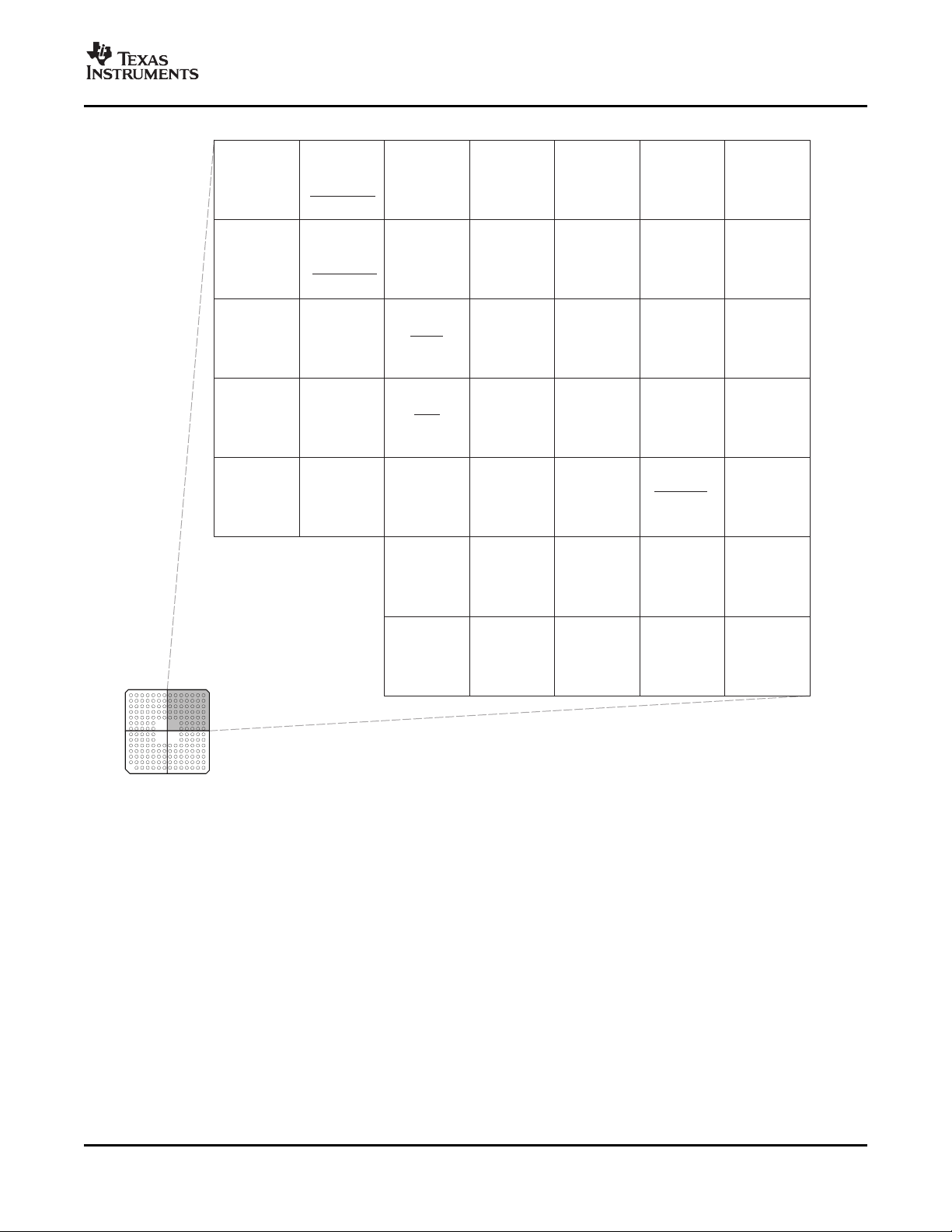
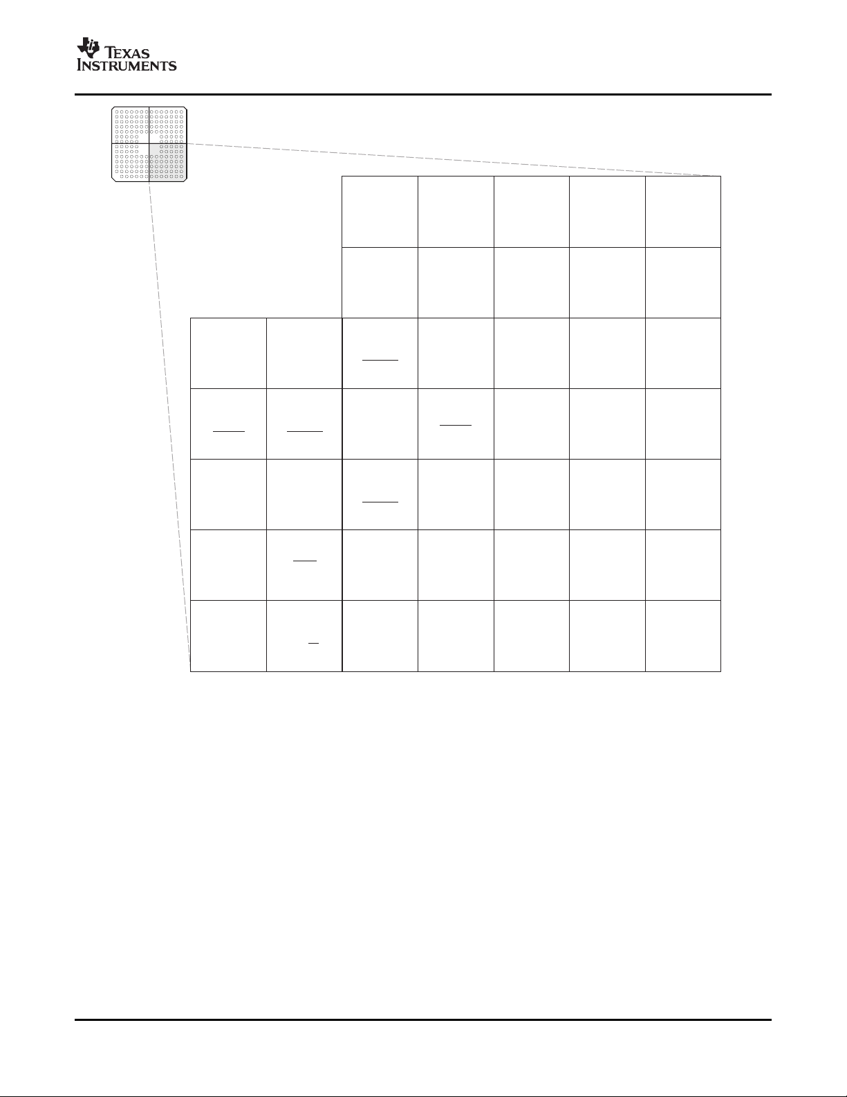
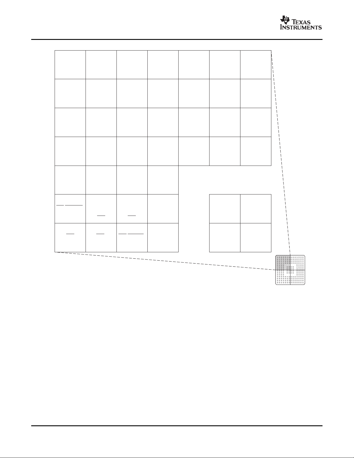
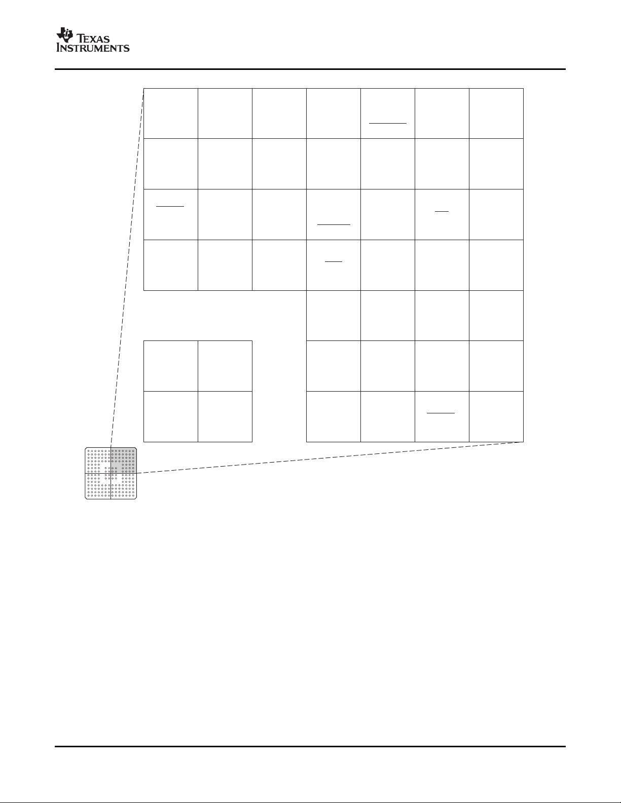
2.1 Pin Assignments
The 176-pin PZ low-profile quad flatpack (LQFP) pin assignments are shown in Figure 2-1 . The 179-ball
ZHH ball grid array (BGA) terminal assignments are shown in Figure 2-2 through Figure 2-5 . The 176-ball
ZJZ plastic ball grid array (PBGA) terminal assignments are shown in Figure 2-6 through
Figure 2-9 .Table 2-3 describes the function(s) of each pin.
Submit Documentation Feedback Introduction 17
Figure 2-1. F2833x, F2823x 176-Pin PGF LQFP (Top View)
www.ti.com
ADVANCE INFORMATION
ADCINB0 ADCINB2 ADCINB6 ADCREFP
ADCINA1
ADCRESEXTADCINA2
ADCLO
ADCINA0 ADCINB4
V
SS1AGND
ADCINA4
ADCINA3 ADCINB3
ADCREFIN
P P
N N
M M
L LADCINA5
GPIO18/
SPICLKA/
SCITXDB/
CANRXA
V
SSA2
ADCINA7 ADCINB7
GPIO17/
SPISOMIA/
CANRXB/
TZ6
V
DD1A18
V
DD
GPIO14/
/
SCITXDB/
MCLKXB
TZ3XHOLD/
GPIO13/
CANRXB/
MDRB
TZ2/
V
DDAIO
K K
J J
H H
1 2 3 4 5
6 7
GPIO20/
EQEP1A/
MDXA/
CANTXB
V
SS2AGND
GPIO21/
EQEP1B/
MDRA/
CANRXB
GPIO22/
EQEP1S/
MCLKXA/
SCITXDB
V
SS
1 2
3
4
5 6
7
V
SSAIO
V
SS
V
DD
V
DD
GPIO23/
EQEP1I/
MFSXA/
SCIRXDB
GPIO19/
SCIRXDB/
CANTXA
SPISTEA/
ADCINA6
GPIO16/
SPISIMOA/
CANTXB/
TZ5
GPIO15/
/
SCIRXDB/
MFSXB
TZ4XHOLDA/
V
DDA2
V
DD2A18
ADCREFMADCINB5ADCINB1
TMS320F28335, TMS320F28334, TMS320F28332
TMS320F28235, TMS320F28234, TMS320F28232
Digital Signal Controllers (DSCs)
SPRS439C – JUNE 2007 – REVISED FEBRUARY 2008
Figure 2-2. F2833x, F2823x 179-Ball ZHH MicroStar BGA™ (Upper Left Quadrant) (Bottom View)
Introduction 18 Submit Documentation Feedback
www.ti.com
ADVANCE INFORMATION
GPIO50/
EQEP1A/
XD29
TMS TEST2
EMU1
GPIO51/
EQEP1B/
XD28
GPIO48/
ECAP5/
XD31
TCK
GPIO52/
EQEP1S/
XD27
V
SS
GPIO27/
ECAP4/
EQEP2S/
MFSXB
XRS
EMU0
GPIO53/
EQEP1I/
XD26
V
DD
GPIO55/
SPISOMIA/
XD24
V
SS
GPIO56/
SPICLKA/
XD23
GPIO58/
MCLKRA/
XD21
GPIO33/
SCLA/
EPWMSYNCO/
ADCSOCBO
TRST
GPIO32/
SDAA/
EPWMSYNCI/
ADCSOCAO
V
DDIO
8 9
10 11 12 13 14
PP
NN
MM
LL
KK
J
J
HH
GPIO57/
/
XD22
SPISTEA
X1
XCLKIN
GPIO59/
MFSRA/
XD20
V
SS
GPIO25/
ECAP2/
EQEP2B/
MDRB
V
SS
V
DD
V
SS
8 9 10
11 12
13
14
V
SS
V
SS
TEST1
V
DD3VFL
GPIO24/
ECAP1/
EQEP2A/
MDXB
GPIO26/
ECAP3/
EQEP2I/
MCLKXB
TDO
V
DDIO
V
SS
X2
GPIO54/
SPISIMOA/
XD25
TDI
V
DDIO
GPIO49/
ECAP6/
XD30
TMS320F28335, TMS320F28334, TMS320F28332
TMS320F28235, TMS320F28234, TMS320F28232
Digital Signal Controllers (DSCs)
SPRS439C – JUNE 2007 – REVISED FEBRUARY 2008
Figure 2-3. F2833x, F2823x 179-Ball ZHH MicroStar BGA™ (Upper Right Quadrant) (Bottom View)
Submit Documentation Feedback Introduction 19

www.ti.com
ADVANCE INFORMATION
GPIO11
EPWM6B
SCIRXDB
ECAP4
/
/
/
GPIO12
CANTXB
MDXB
TZ1//
/
GPIO10
EPWM6A
CANRXB
ADCSOCBO
/
/
/
GPIO9/
EPWM5B/
SCITXDB/
ECAP3
GPIO81/
XA9
GPIO8/
EPWM5A/
CANTXB/
ADCSOCAO
GPIO7/
EPWM4B/
MCLKRA/
ECAP2
GPIO84/
XA12
GPIO6/
EPWM4A/
EPWMSYNCI/
EPWMSYNCO
GPIO4/
EPWM3A
GPIO5/
EPWM3B/
MFSRA/
ECAP1
GPIO3/
EPWM2B/
ECAP5/
MCLKRB
V
DDIO
V
DDIO
V
SS
GPIO2/
EPWM2A
GPIO1/
EPWM1B/
ECAP6/
MFSRB
GPIO86/
XA14
GPIO83/
XA11
G
F
E
D
GPIO0/
EPWM1A
GPIO29/
SCITXDA/
XA19
V
SS
GPIO85/
XA13
GPIO82/
XA10
V
DD
GPIO30/
CANRXA/
XA18
GPIO39/
XA16
V
SS
V
DD
GPIO31/
CANTXA/
XA17
GPIO87/
XA15
V
DDIO
C
B
A
1 2 3 4 5 6 7
G
F
E
D
C
B
A
V
SS
GPIO45/
XA5
V
SS
GPIO80/
XA8
GPIO46/
XA6
GPIO43/
XA3
GPIO44/
XA4
GPIO47/
XA7
V
SS
1 2 3 4 5
6 7
V
SS
V
DD
V
SS
TMS320F28335, TMS320F28334, TMS320F28332
TMS320F28235, TMS320F28234, TMS320F28232
Digital Signal Controllers (DSCs)
SPRS439C – JUNE 2007 – REVISED FEBRUARY 2008
Figure 2-4. F2833x, F2823x 179-Ball ZHH MicroStar BGA™ (Lower Left Quadrant) (Bottom View)
Introduction 20 Submit Documentation Feedback
www.ti.com
ADVANCE INFORMATION
GPIO60/
MCLKRB/
XD19
GPIO64/
XD15
GPIO63/
SCITXDC/
XD16
GPIO61/
MFSRB/
XD18
GPIO67/
XD12
GPIO65/
XD14
GPIO62/
SCIRXDC
XD17
GPIO78/
XD1
GPIO79/
XD0
GPIO66/
XD13
GPIO68/
XD11
V
SS
GPIO37/
ECAP2/
XZCS7
GPIO34/
ECAP1/
XREADY
GPIO38/
XWE0
GPIO70/
XD9
G
F
E
D
V
DD
GPIO40/
XA0/
XWE1
V
SS
XCLKOUT
GPIO73/
XD6
GPIO42/
XA2
XRD
GPIO28/
SCIRXDA/
XZCS6
V
DD
GPIO35/
SCITXDA/
XR/W
GPIO69/
XD10
V
DDIO
C
B
A
8 9 10 11 12 13 14
G
F
E
D
C
B
A
GPIO74/
XD5
GPIO76/
XD3
GPIO72/
XD7
GPIO75/
XD4
GPIO77/
XD2
V
SS
GPIO41/
XA1
V
SS
V
DD
V
SS
8 9
10 11 12 13 14
V
SS
V
DD
V
SS
V
DDIO
GPIO36/
SCIRXDA/
XZCS0
V
DD
GPIO71/
XD8
TMS320F28335, TMS320F28334, TMS320F28332
TMS320F28235, TMS320F28234, TMS320F28232
Digital Signal Controllers (DSCs)
SPRS439C – JUNE 2007 – REVISED FEBRUARY 2008
Figure 2-5. F2833x, F2823x 179-Ball ZHH MicroStar BGA ™(Lower Right Quadrant) (Bottom View)
Submit Documentation Feedback Introduction 21
www.ti.com
ADVANCE INFORMATION
V
SSA2
ADCINB0 ADCREFM ADCREFP ADCRESEXT ADCREFIN
V
SSAIO
ADCLO
ADCINB1
ADCINB3
ADCINB5 ADCINB7
EMU0
ADCINA2 ADCINA1 ADCINA0 ADCINB2 ADCINB4 ADCINB6 TEST1
ADCINA5 ADCINA4
ADCINA3
V
SS1AGND
V
DDAIO
V
DD2A18
TEST2
ADCINA7 ADCINA6
V
DD1A18
V
DDA2
GPIO15/
/ /
SCIRXDB/
MFSXB
TZ4XHOLDA
GPIO16/
SPISIMOA/
CANTXB/
TZ5
GPIO17/
SPISOMIA/
CANRXB/
TZ6
V
DD
V
SS
V
SS
GPIO14/
/TZ3XHOLD/
SCITXDB/
MCLKXB
V
DD
V
SS
V
SS
P
N
M
L
K
J
H
1 2 3 4 5 6 7
V
SS2AGND
GPIO12/
TZ1/
CANTXB/
MDXB
GPIO13/
TZ2/
CANRXB/
MDRB
TMS320F28335, TMS320F28334, TMS320F28332
TMS320F28235, TMS320F28234, TMS320F28232
Digital Signal Controllers (DSCs)
SPRS439C – JUNE 2007 – REVISED FEBRUARY 2008
Figure 2-6. F2833x, F2823x 176-Ball ZJZ Plastic BGA (Upper Left Quadrant) (Bottom View)
Introduction 22 Submit Documentation Feedback
www.ti.com
ADVANCE INFORMATION
V
SS
V
SS
V
SS
V
SS
P
N
M
L
K
J
H
8 9 10 11 12 13 14
EMU1
GPIO20/
EQEP1A/
MDXA/
CANTXB
GPIO23/
EQEP1I/
MFSXA/
SCIRXDB
GPIO26/
ECAP3/
EQEP2I/
MCLKXB
GPIO33/
SCLA/
EPWMSYNCO/
ADCSOCBO
V
SS
V
SS
GPIO18/
SPICLKA/
SCITXDB/
CANRXA
GPIO21/
EQEP1B/
MDRA/
CANRXB
GPIO24/
ECAP1/
EQEP2A/
MDXB
GPIO27/
ECAP4/
EQEP2S/
MFSXB
TDI
TDO
V
DDIO
GPIO19/
/
SCIRXDB/
CANTXA
SPISTEA
GPIO22/
EQEP1S/
MCLKXA/
SCITXDB
GPIO25/
ECAP2/
EQEP2B/
MDRB
GPIO32/
SDAA/
EPWMSYNCI/
ADSOCAO
TMS
XRS
TCK
V
DD
V
DD3VFL
V
DDIO
TRST
GPIO50/
EQEP1A/
XD29
GPIO49/
ECAP6/
XD30
GPIO48/
ECAP5/
XD31
V
DD
GPIO53
EQEP1I/
XD26
GPIO52/
EQEP1S/
XD27
GPIO51/
EQEP1B/
XD28
V
DD
GPIO56/
SPICLKA/
XD23
GPIO55/
SPISOMIA/
XD24
GPIO54/
SPISIMOA/
XD25
GPIO59/
MFSRA/
XD20
GPIO58/
MCLKRA/
XD21
GPIO57/
/
XD22
SPISTEA
X2
TMS320F28335, TMS320F28334, TMS320F28332
TMS320F28235, TMS320F28234, TMS320F28232
Digital Signal Controllers (DSCs)
SPRS439C – JUNE 2007 – REVISED FEBRUARY 2008
Figure 2-7. F2833x, F2823x 176-Ball ZJZ Plastic BGA (Upper Right Quadrant) (Bottom View)
Submit Documentation Feedback Introduction 23

www.ti.com
ADVANCE INFORMATION
G
F
E
D
C
B
A
1 2 3 4 5 6 7
GPIO9/
EPWM5B/
SCITXDB/
ECAP3
GPIO10/
EPWM6A/
CANRXB/
ADCSOCBO
GPIO11/
EPWM6B/
SCIRXDB/
ECAP4
V
DDIO
V
SS
V
SS
V
SS
V
SS
GPIO6/
EPWM4A/
EPWMSYNCI/
EPWMSYNCO
GPIO7/
EPWM4B/
MCLKRA/
ECAP2
GPIO8/
EPWM5A/
CANTXB/
ADCSOCAO
V
DD
GPIO3/
EPWM2B/
ECAP5/
MCLKRB
GPIO4/
EPWM3A
GPIO5/
EPWM3B/
MFSRA/
ECAP1
V
DDIO
GPIO0/
EPWM1A
GPIO1/
EPWM1B/
ECAP6/
MFSRB
GPIO2/
EPWM2A
V
DD
V
DD
GPIO47/
XA7
V
DDIO
GPIO29/
SCITXDA/
XA19
GPIO30/
CANRXA/
XA18
GPIO39/
XA16
GPIO85/
XA13
GPIO82/
XA10
GPIO46/
XA6
GPIO43/
XA3
V
DDIO
GPIO31/
CANTXA/
XA17
GPIO87/
XA15
GPIO84/
XA12
GPIO81/
XA9
GPIO45/
XA5
GPIO42/
XA2
V
SS
V
SS
GPIO86/
XA14
GPIO83/
XA11
GPIO80/
XA8
GPIO44/
XA4
GPIO41/
XA1
TMS320F28335, TMS320F28334, TMS320F28332
TMS320F28235, TMS320F28234, TMS320F28232
Digital Signal Controllers (DSCs)
SPRS439C – JUNE 2007 – REVISED FEBRUARY 2008
Figure 2-8. F2833x, F2823x 176-Ball ZJZ Plastic BGA (Lower Left Quadrant) (Bottom View)
Introduction 24 Submit Documentation Feedback
www.ti.com
ADVANCE INFORMATION
G
F
E
D
C
B
A
8 9 10 11 12 13 14
X1
V
SS
V
SS
V
SS
V
SS
V
DDIO
GPIO60/
MCLKRB/
XD19
XCLKIN
V
DD
GPIO63/
SCITXDC/
XD16
GPIO62/
SCIRXDC/
XD17
GPIO61/
MFSRB/
XD18
V
DD
GPIO66/
XD13
GPIO65/
XD14
GPIO64/
XD15
V
DD
V
DD
GPIO28/
SCIRXDA/
XZCS6
V
DDIO
GPIO69/
XD10
GPIO68/
XD11
GPIO67/
XD12
GPIO40/
XA0/XWE1
GPIO36/
SCIRXDA/
XZCS0
GPIO38/
XWE0
GPIO78/
XD1
GPIO75/
XD4
GPIO71/
XD8
GPIO70/
XD9
GPIO37/
ECAP2/
XZCS7
GPIO35/
SCITXDA/
XR/W
GPIO79/
XD0
GPIO77/
XD2
GPIO74/
XD5
GPIO72
XD7
V
SS
V
SS
XRD
GPIO34/
ECAP1/
XREADY
XCLKOUT
GPIO76/
XD3
GPIO73/
XD6
V
DDIO
TMS320F28335, TMS320F28334, TMS320F28332
TMS320F28235, TMS320F28234, TMS320F28232
Digital Signal Controllers (DSCs)
SPRS439C – JUNE 2007 – REVISED FEBRUARY 2008
Figure 2-9. F2833x, F2823x 176-Ball ZJZ Plastic BGA (Lower Right Quadrant) (Bottom View)
Submit Documentation Feedback Introduction 25
www.ti.com
ADVANCE INFORMATION
TMS320F28335, TMS320F28334, TMS320F28332
TMS320F28235, TMS320F28234, TMS320F28232
Digital Signal Controllers (DSCs)
SPRS439C – JUNE 2007 – REVISED FEBRUARY 2008
2.2 Signal Descriptions
Table 2-3 describes the signals. The GPIO function (shown in Italics) is the default at reset. The peripheral
signals that are listed under them are alternate functions. Some peripheral functions may not be available
in all devices. See Table 2-1 for details. Inputs are not 5-V tolerant. All XINTF pins have a drive strength
of 8 mA (typical), with the exception of XREADY, which is 4 mA (typical). All GPIO pins are I/O/Z, 4-mA
drive typical (unless otherwise indicated), and have an internal pullup, which can be selectively
enabled/disabled on a per-pin basis. This feature only applies to the GPIO pins. The pullups on
GPIO0-GPIO11 pins are not enabled at reset. The pullups on GPIO12-GPIO34 are enabled upon reset.
Table 2-3. Signal Descriptions
PIN NO.
NAME DESCRIPTION
TRST 78 M10 L11
TCK 87 N12 M14 JTAG test clock with internal pullup (I, ↑ )
TMS 79 P10 M12
TDI 76 M9 N12
TDO 77 K9 N13
EMU0 85 L11 N7 (I/O/Z, 8 mA drive ↑ )
EMU1 86 P12 P8 (I/O/Z, 8 mA drive ↑ )
V
DD3VFL
TEST1 81 K10 M7 Test Pin. Reserved for TI. Must be left unconnected. (I/O)
TEST2 82 P11 L7 Test Pin. Reserved for TI. Must be left unconnected. (I/O)
XCLKOUT 138 C11 A10 and bit 2 (CLKMODE) in the XINTCNF2 register. At reset, XCLKOUT = SYSCLKOUT/4. The
PGF ZHH ZJZ
PIN BAL BAL
# L # L #
JTAG
JTAG test reset with internal pulldown. TRST, when driven high, gives the scan system control of
the operations of the device. If this signal is not connected or driven low, the device operates in its
functional mode, and the test reset signals are ignored.
NOTE: TRST is an active high test pin and must be maintained low at all times during normal
device operation. An external pulldown resistor is recommended on this pin. The value of this
resistor should be based on drive strength of the debugger pods applicable to the design. A 2.2-k Ω
resistor generally offers adequate protection. Since this is application-specific, it is recommended
that each target board be validated for proper operation of the debugger and the application. (I, ↓ )
JTAG test-mode select (TMS) with internal pullup. This serial control input is clocked into the TAP
controller on the rising edge of TCK. (I, ↑ )
JTAG test data input (TDI) with internal pullup. TDI is clocked into the selected register (instruction
or data) on a rising edge of TCK. (I, ↑ )
JTAG scan out, test data output (TDO). The contents of the selected register (instruction or data)
are shifted out of TDO on the falling edge of TCK. (O/Z 8 mA drive)
Emulator pin 0. When TRST is driven high, this pin is used as an interrupt to or from the emulator
system and is defined as input/output through the JTAG scan. This pin is also used to put the
device into boundary-scan mode. With the EMU0 pin at a logic-high state and the EMU1 pin at a
logic-low state, a rising edge on the TRST pin would latch the device into boundary-scan mode.
NOTE: An external pullup resistor is recommended on this pin. The value of this resistor should be
based on the drive strength of the debugger pods applicable to the design. A 2.2-k Ω to 4.7-k Ω
resistor is generally adequate. Since this is application-specific, it is recommended that each target
board be validated for proper operation of the debugger and the application.
Emulator pin 1. When TRST is driven high, this pin is used as an interrupt to or from the emulator
system and is defined as input/output through the JTAG scan. This pin is also used to put the
device into boundary-scan mode. With the EMU0 pin at a logic-high state and the EMU1 pin at a
logic-low state, a rising edge on the TRST pin would latch the device into boundary-scan mode.
NOTE: An external pullup resistor is recommended on this pin. The value of this resistor should be
based on the drive strength of the debugger pods applicable to the design. A 2.2-k Ω to 4.7-k Ω
resistor is generally adequate. Since this is application-specific, it is recommended that each target
board be validated for proper operation of the debugger and the application.
FLASH
84 M11 L9 3.3-V Flash Core Power Pin. This pin should be connected to 3.3 V at all times.
CLOCK
Output clock derived from SYSCLKOUT. XCLKOUT is either the same frequency, one-half the
frequency, or one-fourth the frequency of SYSCLKOUT. This is controlled by bits 18:16 (XTIMCLK)
XCLKOUT signal can be turned off by setting XINTCNF2[CLKOFF] to 1. Unlike other GPIO pins,
the XCLKOUT pin is not placed in high-impedance state during a reset. (O/Z, 8 mA drive).
(1)
(1) I = Input, O = Output, Z = High impedance, OD = Open drain, ↑ = Pullup, ↓ = Pulldown
Introduction 26 Submit Documentation Feedback
www.ti.com
ADVANCE INFORMATION
TMS320F28335, TMS320F28334, TMS320F28332
TMS320F28235, TMS320F28234, TMS320F28232
Digital Signal Controllers (DSCs)
SPRS439C – JUNE 2007 – REVISED FEBRUARY 2008
Table 2-3. Signal Descriptions (continued)
PIN NO.
NAME DESCRIPTION
XCLKIN 105 J14 G13 the X1 pin must be tied to GND. If a crystal/resonator is used (or if an external 1.9-V oscillator is
X1 104 J13 G14 power supply. A 1.9-V external oscillator may be connected to the X1 pin. In this case, the XCLKIN
X2 102 J11 H14
XRS 80 L10 M13
ADCINA7 35 K4 K1 ADC Group A, Channel 7 input (I)
ADCINA6 36 J5 K2 ADC Group A, Channel 6 input (I)
ADCINA5 37 L1 L1 ADC Group A, Channel 5 input (I)
ADCINA4 38 L2 L2 ADC Group A, Channel 4 input (I)
ADCINA3 39 L3 L3 ADC Group A, Channel 3 input (I)
ADCINA2 40 M1 M1 ADC Group A, Channel 2 input (I)
ADCINA1 41 N1 M2 ADC Group A, Channel 1 input (I)
ADCINA0 42 M3 M3 ADC Group A, Channel 0 input (I)
ADCINB7 53 K5 N6 ADC Group B, Channel 7 input (I)
ADCINB6 52 P4 M6 ADC Group B, Channel 6 input (I)
ADCINB5 51 N4 N5 ADC Group B, Channel 5 input (I)
ADCINB4 50 M4 M5 ADC Group B, Channel 4 input (I)
ADCINB3 49 L4 N4 ADC Group B, Channel 3 input (I)
ADCINB2 48 P3 M4 ADC Group B, Channel 2 input (I)
ADCINB1 47 N3 N3 ADC Group B, Channel 1 input (I)
ADCINB0 46 P2 P3 ADC Group B, Channel 0 input (I)
ADCLO 43 M2 N2 Low Reference (connect to analog ground) (I)
ADCRESEXT 57 M5 P6 ADC External Current Bias Resistor. Connect a 22-k Ω resistor to analog ground.
ADCREFIN 54 L5 P7 External reference input (I)
ADCREFP 56 P5 P5
ADCREFM 55 N5 P4
V
DDA2
V
SSA2
V
DDAIO
V
SSAIO
V
DD1A18
V
SS1AGND
PGF ZHH ZJZ
PIN BAL BAL
# L # L #
External Oscillator Input. This pin is to feed a clock from an external 3.3-V oscillator. In this case,
used to feed clock to X1 pin), this pin must be tied to GND. (I)
Internal/External Oscillator Input. To use the internal oscillator, a quartz crystal or a ceramic
resonator may be connected across X1 and X2. The X1 pin is referenced to the 1.9-V core digital
pin must be connected to ground. If a 3.3-V external oscillator is used with the XCLKIN pin, X1
must be tied to GND. (I)
Internal Oscillator Output. A quartz crystal or a ceramic resonator may be connected across X1 and
X2. If X2 is not used it must be left unconnected. (O)
RESET
Device Reset (in) and Watchdog Reset (out).
Device reset. XRS causes the device to terminate execution. The PC will point to the address
contained at the location 0x3FFFC0. When XRS is brought to a high level, execution begins at the
location pointed to by the PC. This pin is driven low by the DSC when a watchdog reset occurs.
During watchdog reset, the XRS pin is driven low for the watchdog reset duration of 512 OSCCLK
cycles. (I/OD, ↑ )
The output buffer of this pin is an open-drain with an internal pullup. It is recommended that this pin
be driven by an open-drain device.
ADC SIGNALS
Internal Reference Positive Output. Requires a low ESR (50 m Ω - 1.5 Ω ) ceramic bypass capacitor
of 2.2 µ F to analog ground. (O)
Internal Reference Medium Output. Requires a low ESR (50 m Ω - 1.5 Ω ) ceramic bypass capacitor
of 2.2 µ F to analog ground. (O)
CPU AND I/O POWER PINS
34 K2 K4 ADC Analog Power Pin
33 K3 P1 ADC Analog Ground Pin
45 N2 L5 ADC Analog I/O Power Pin
44 P1 N1 ADC Analog I/O Ground Pin
31 J4 K3 ADC Analog Power Pin
32 K1 L4 ADC Analog Ground Pin
(1)
Submit Documentation Feedback Introduction 27
www.ti.com
ADVANCE INFORMATION
TMS320F28335, TMS320F28334, TMS320F28332
TMS320F28235, TMS320F28234, TMS320F28232
Digital Signal Controllers (DSCs)
SPRS439C – JUNE 2007 – REVISED FEBRUARY 2008
Table 2-3. Signal Descriptions (continued)
PIN NO.
NAME DESCRIPTION
V
DD2A18
V
SS2AGND
V
DD
V
DD
V
DD
V
DD
V
DD
V
DD
V
DD
V
DD
V
DD
V
DD
V
DD
V
DD
V
DD
V
DDIO
V
DDIO
V
DDIO
V
DDIO
V
DDIO
V
DDIO
V
DDIO
V
DDIO
V
DDIO
V
SS
V
SS
V
SS
V
SS
V
SS
V
SS
V
SS
V
SS
V
SS
V
SS
V
SS
V
SS
V
SS
V
SS
V
SS
V
SS
V
SS
V
SS
V
SS
V
SS
PGF ZHH ZJZ
PIN BAL BAL
# L # L #
59 M6 L6 ADC Analog Power Pin
58 K6 P2 ADC Analog Ground Pin
4 B1 D4
15 B5 D5
23 B11 D8
29 C8 D9
61 D13 E11
101 E9 F4
109 F3 F11 CPU and Logic Digital Power Pins
117 F13 H4
126 H1 J4
139 H12 J11
146 J2 K11
154 K14 L8
167 N6
9 A4 A13
71 B10 B1
93 E7 D7
107 E12 D11
121 F5 E4 Digital I/O Power Pin
143 L8 G4
159 H11 G11
170 N14 L10
N14
3 A5 A1
8 A10 A2
14 A11 A14
22 B4 B14
30 C3 F6
60 C7 F7
70 C9 F8
83 D1 F9
92 D6 G6
103 D14 G7
Digital Ground Pins
106 E8 G8
108 E14 G9
118 F4 H6
120 F12 H7
125 G1 H8
140 H10 H9
144 H13 J6
147 J3 J7
155 J10 J8
160 J12 J9
(1)
Introduction 28 Submit Documentation Feedback
www.ti.com
ADVANCE INFORMATION
TMS320F28335, TMS320F28334, TMS320F28332
TMS320F28235, TMS320F28234, TMS320F28232
Table 2-3. Signal Descriptions (continued)
PIN NO.
NAME DESCRIPTION
V
SS
V
SS
V
SS
V
SS
V
SS
GPIO0 General purpose input/output 0 (I/O/Z)
EPWM1A Enhanced PWM1 Output A and HRPWM channel (O)
- -
- GPIO1 General purpose input/output 1 (I/O/Z)
EPWM1B Enhanced PWM1 Output B (O)
ECAP6 Enhanced Capture 6 input/output (I/O)
MFSRB McBSP-B receive frame synch (I/O)
GPIO2 General purpose input/output 2 (I/O/Z)
EPWM2A Enhanced PWM2 Output A and HRPWM channel (O)
- -
- GPIO3 General purpose input/output 3 (I/O/Z)
EPWM2B Enhanced PWM2 Output B (O)
ECAP5 Enhanced Capture 5 input/output (I/O)
MCLKRB McBSP-B receive clock (I/O)
GPIO4 General purpose input/output 4 (I/O/Z)
EPWM3A Enhanced PWM3 output A and HRPWM channel (O)
- -
- GPIO5 General purpose input/output 5 (I/O/Z)
EPWM3B Enhanced PWM3 output B (O)
MFSRA McBSP-A receive frame synch (I/O)
ECAP1 Enhanced Capture input/output 1 (I/O)
GPIO6 General purpose input/output 6 (I/O/Z)
EPWM4A Enhanced PWM4 output A and HRPWM channel (O)
EPWMSYNCI External ePWM sync pulse input (I)
EPWMSYNCO External ePWM sync pulse output (O)
GPIO7 General purpose input/output 7 (I/O/Z)
EPWM4B Enhanced PWM4 output B (O)
MCLKRA McBSP-A receive clock (I/O)
ECAP2 Enhanced capture input/output 2 (I/O)
GPIO8 General Purpose Input/Output 8 (I/O/Z)
EPWM5A Enhanced PWM5 output A and HRPWM channel (O)
CANTXB Enhanced CAN-B transmit (O)
ADCSOCAO ADC start-of-conversion A (O)
GPIO9 General purpose input/output 9 (I/O/Z)
EPWM5B Enhanced PWM5 output B (O)
SCITXDB SCI-B transmit data(O)
ECAP3 Enhanced capture input/output 3 (I/O)
GPIO10 General purpose input/output 10 (I/O/Z)
EPWM6A Enhanced PWM6 output A and HRPWM channel (O)
CANRXB Enhanced CAN-B receive (I)
ADCSOCBO ADC start-of-conversion B (O)
GPIO11 General purpose input/output 11 (I/O/Z)
EPWM6B Enhanced PWM6 output B (O)
SCIRXDB SCI-B receive data (I)
ECAP4 Enhanced CAP Input/Output 4 (I/O)
PGF ZHH ZJZ
PIN BAL BAL
# L # L #
166 M12 P13
171 N10 P14
N11
P6
P8
5 C1 D1
6 D3 D2
7 D2 D3
10 E4 E1
11 E2 E2
12 E3 E3
13 E1 F1
16 F2 F2
17 F1 F3
18 G5 G1
19 G4 G2
20 G2 G3
Digital Ground Pins
GPIOA AND PERIPHERAL SIGNALS
Digital Signal Controllers (DSCs)
SPRS439C – JUNE 2007 – REVISED FEBRUARY 2008
(1)
Submit Documentation Feedback Introduction 29
www.ti.com
ADVANCE INFORMATION
TMS320F28335, TMS320F28334, TMS320F28332
TMS320F28235, TMS320F28234, TMS320F28232
Digital Signal Controllers (DSCs)
SPRS439C – JUNE 2007 – REVISED FEBRUARY 2008
Table 2-3. Signal Descriptions (continued)
PIN NO.
NAME DESCRIPTION
GPIO12 General purpose input/output 12 (I/O/Z)
TZ1 Trip Zone input 1 (I)
CANTXB Enhanced CAN-B transmit (O)
MDXB McBSP-B transmit serial data (O)
GPIO13 General purpose input/output 13 (I/O/Z)
TZ2 Trip Zone input 2 (I)
CANRXB Enhanced CAN-B receive (I)
MDRB McBSP-B receive serial data (I)
GPIO14 General purpose input/output 14 (I/O/Z)
TZ3/ XHOLD XINTCNF2[HOLD] = 1. If this is not done, the XINTF bus will go into high impedance anytime TZ3
SCITXDB SCI-B Transmit (I)
MCLKXB McBSP-B transmit clock (I/O)
GPIO15 General purpose input/output 15 (I/O/Z)
TZ4/ XHOLDA
SCIRXDB SCI-B receive (I)
MFSXB McBSP-B transmit frame synch (I/O)
GPIO16 General purpose input/output 16 (I/O/Z)
SPISIMOA SPI slave in, master out (I/O)
CANTXB Enhanced CAN-B transmit (O)
TZ5 Trip Zone input 5 (I)
GPIO17 General purpose input/output 17 (I/O/Z)
SPISOMIA SPI-A slave out, master in (I/O)
CANRXB Enhanced CAN-B receive (I)
TZ6 Trip zone input 6 (I)
GPIO18 General purpose input/output 18 (I/O/Z)
SPICLKA SPI-A clock input/output (I/O)
SCITXDB SCI-B transmit (O)
CANRXA Enhanced CAN-A receive (I)
GPIO19 General purpose input/output 19 (I/O/Z)
SPISTEA SPI-A slave transmit enable input/output (I/O)
SCIRXDB SCI-B receive (I)
CANTXA Enhanced CAN-A transmit (O)
GPIO20 General purpose input/output 20 (I/O/Z)
EQEP1A Enhanced QEP1 input A (I)
MDXA McBSP-A transmit serial data (O)
CANTXB Enhanced CAN-B transmit (O)
GPIO21 General purpose input/output 21 (I/O/Z)
EQEP1B Enhanced QEP1 input B (I)
MDRA McBSP-A receive serial data (I)
CANRXB Enhanced CAN-B receive (I)
GPIO22 General purpose input/output 22 (I/O/Z)
EQEP1S Enhanced QEP1 strobe (I/O)
MCLKXA McBSP-A transmit clock (I/O)
SCITXDB SCI-B transmit (O)
PGF ZHH ZJZ
PIN BAL BAL
# L # L #
21 G3 H1
24 H3 H2
Trip Zone input 3/External Hold Request. XHOLD, when active (low), requests the external interface
(XINTF) to release the external bus and place all buses and strobes into a high-impedance state.
To prevent this from happening when TZ3 signal goes active, disable this function by writing
25 H2 H3
26 H4 J1 active (low) when the XINTF has granted an XHOLD request. All XINTF buses and strobe signals
27 H5 J2
28 J1 J3
62 L6 N8
63 K7 M8
64 L7 P9
65 P7 N9
66 N7 M9
goes low. On the ePWM side, TZn signals are ignored by default, unless they are enabled by the
code. The XINTF will release the bus when any current access is complete and there are no
pending accesses on the XINTF. (I)
Trip Zone input 4/External Hold Acknowledge. The pin function for this option is based on the
direction chosen in the GPADIR register. If the pin is configured as an input, then TZ4 function is
chosen. If the pin is configured as an output, then XHOLDA function is chosen. XHOLDA is driven
will be in a high-impedance state. XHOLDA is released when the XHOLD signal is released.
External devices should only drive the external bus when XHOLDA is active (low). (I/0)
(1)
Introduction 30 Submit Documentation Feedback
www.ti.com
ADVANCE INFORMATION
TMS320F28335, TMS320F28334, TMS320F28332
TMS320F28235, TMS320F28234, TMS320F28232
Table 2-3. Signal Descriptions (continued)
PIN NO.
NAME DESCRIPTION
GPIO23 General purpose input/output 23 (I/O/Z)
EQEP1I Enhanced QEP1 index (I/O)
MFSXA McBSP-A transmit frame synch (I/O)
SCIRXDB SCI-B receive (I)
GPIO24 General purpose input/output 24 (I/O/Z)
ECAP1 Enhanced capture 1 (I/O)
EQEP2A Enhanced QEP2 input A (I)
MDXB McBSP-B transmit serial data (O)
GPIO25 General purpose input/output 25 (I/O/Z)
ECAP2 Enhanced capture 2 (I/O)
EQEP2B Enhanced QEP2 input B (I)
MDRB McBSP-B receive serial data (I)
GPIO26 General purpose input/output 26 (I/O/Z)
ECAP3 Enhanced capture 3 (I/O)
EQEP2I Enhanced QEP2 index (I/O)
MCLKXB McBSP-B transmit clock (I/O)
GPIO27 General purpose input/output 27 (I/O/Z)
ECAP4 Enhanced capture 4 (I/O)
EQEP2S Enhanced QEP2 strobe (I/O)
MFSXB McBSP-B transmit frame synch (I/O)
GPIO28 General purpose input/output 28 (I/O/Z)
SCIRXDA 141 E10 D10 SCI receive data (I)
XZCS6 External Interface zone 6 chip select (O)
GPIO29 General purpose input/output 29. (I/O/Z)
SCITXDA 2 C2 C1 SCI transmit data (O)
XA19 External Interface Address Line 19 (O)
GPIO30 General purpose input/output 30 (I/O/Z)
CANRXA 1 B2 C2 Enhanced CAN-A receive (I)
XA18 External Interface Address Line 18 (O)
GPIO31 General purpose input/output 31 (I/O/Z)
CANTXA 176 A2 B2 Enhanced CAN-A transmit (O)
XA17 External Interface Address Line 17 (O)
GPIO32 General purpose input/output 32 (I/O/Z)
SDAA I2C data open-drain bidirectional port (I/OD)
EPWMSYNCI Enhanced PWM external sync pulse input (I)
ADCSOCAO ADC start-of-conversion A (O)
GPIO33 General-Purpose Input/Output 33 (I/O/Z)
SCLA I2C clock open-drain bidirectional port (I/OD)
EPWMSYNCO Enhanced PWM external synch pulse output (O)
ADCSOCBO ADC start-of-conversion B (O)
GPIO34 General-Purpose Input/Output 34 (I/O/Z)
ECAP1 142 D10 A9 Enhanced Capture input/output 1 (I/O)
XREADY External Interface Ready signal
GPIO35 General-Purpose Input/Output 35 (I/O/Z)
SCITXDA 148 A9 B9 SCI-A transmit data (O)
XR/ W External Interface read, not write strobe
GPIO36 General-Purpose Input/Output 36 (I/O/Z)
SCIRXDA 145 C10 C9 SCI receive data (I)
XZCS0 External Interface zone 0 chip select (O)
GPIO37 General-Purpose Input/Output 37 (I/O/Z)
ECAP2 150 D9 B8 Enhanced Capture input/output 2 (I/O)
XZCS7 External Interface zone 7 chip select (O)
GPIO38 General-Purpose Input/Output 38 (I/O/Z)
- 137 D11 C10 XWE0 External Interface Write Enable 0 (O)
GPIO39 General-Purpose Input/Output 39 (I/O/Z)
- 175 B3 C3 XA16 External Interface Address Line 16 (O)
PGF ZHH ZJZ
PIN BAL BAL
# L # L #
67 M7 P10
68 M8 N10
69 N8 M10
72 K8 P11
73 L9 N11
74 N9 M11
75 P9 P12
Digital Signal Controllers (DSCs)
SPRS439C – JUNE 2007 – REVISED FEBRUARY 2008
(1)
Submit Documentation Feedback Introduction 31

www.ti.com
ADVANCE INFORMATION
TMS320F28335, TMS320F28334, TMS320F28332
TMS320F28235, TMS320F28234, TMS320F28232
Digital Signal Controllers (DSCs)
SPRS439C – JUNE 2007 – REVISED FEBRUARY 2008
Table 2-3. Signal Descriptions (continued)
PIN NO.
NAME DESCRIPTION
GPIO40 General-Purpose Input/Output 40 (I/O/Z)
- 151 D8 C8 XA0/ XWE1 External Interface Address Line 0/External Interface Write Enable 1 (O)
GPIO41 General-Purpose Input/Output 41 (I/O/Z)
- 152 A8 A7 XA1 External Interface Address Line 1 (O)
GPIO42 General-Purpose Input/Output 42 (I/O/Z)
- 153 B8 B7 XA2 External Interface Address Line 2 (O)
GPIO43 General-Purpose Input/Output 43 (I/O/Z)
- 156 B7 C7 XA3 External Interface Address Line 3 (O)
GPIO44 General-Purpose Input/Output 44 (I/O/Z)
- 157 A7 A6 XA4 External Interface Address Line 4 (O)
GPIO45 General-Purpose Input/Output 45 (I/O/Z)
- 158 D7 B6 XA5 External Interface Address Line 5 (O)
GPIO46 General-Purpose Input/Output 46 (I/O/Z)
- 161 B6 C6 XA6 External Interface Address Line 6 (O)
GPIO47 General-Purpose Input/Output 47 (I/O/Z)
- 162 A6 D6 XA7 External Interface Address Line 7 (O)
GPIO48 General-Purpose Input/Output 48 (I/O/Z)
ECAP5 88 P13 L14 Enhanced Capture input/output 5 (I/O)
XD31 External Interface Data Line 31 (O)
GPIO49 General-Purpose Input/Output 49 (I/O/Z)
ECAP6 89 N13 L13 Enhanced Capture input/output 6 (I/O)
XD30 External Interface Data Line 30 (O)
GPIO50 General-Purpose Input/Output 50 (I/O/Z)
EQEP1A 90 P14 L12 Enhanced QEP 1input A (I)
XD29 External Interface Data Line 29 (O)
GPIO51 General-Purpose Input/Output 51 (I/O/Z)
EQEP1B 91 M13 K14 Enhanced QEP 1input B (I)
XD28 External Interface Data Line 28 (O)
GPIO52 General-Purpose Input/Output 52 (I/O/Z)
EQEP1S 94 M14 K13 Enhanced QEP 1Strobe (I/O)
XD27 External Interface Data Line 27 (O)
GPIO53 General-Purpose Input/Output 53 (I/O/Z)
EQEP1I 95 L12 K12 Enhanced CAP1 lndex (I/O)
XD26 External Interface Data Line 26 (O)
GPIO54 General-Purpose Input/Output 54 (I/O/Z)
SPISIMOA 96 L13 J14 SPI-A slave in, master out (I/O)
XD25 External Interface Data Line 25 (O)
GPIO55 General-Purpose Input/Output 55 (I/O/Z)
SPISOMIA 97 L14 J13 SPI-A slave out, master in (I/O)
XD24 External Interface Data Line 24 (O)
GPIO56 General-Purpose Input/Output 56 (I/O/Z)
SPICLKA 98 K11 J12 SPI-A clock (I/O)
XD23 External Interface Data Line 23 (O)
GPIO57 General-Purpose Input/Output 57 (I/O/Z)
SPISTEA 99 K13 H13 SPI-A slave transmit enable (I/O)
XD22 External Interface Data Line 22 (O)
GPIO58 General-Purpose Input/Output 58 (I/O/Z)
MCLKRA 100 K12 H12 McBSP-A receive clock (I/O)
XD21 External Interface Data Line 21 (O)
PGF ZHH ZJZ
PIN BAL BAL
# L # L #
(1)
Introduction 32 Submit Documentation Feedback

www.ti.com
ADVANCE INFORMATION
Table 2-3. Signal Descriptions (continued)
PIN NO.
NAME DESCRIPTION
GPIO59 General-Purpose Input/Output 59 (I/O/Z)
MFSRA 110 H14 H11 McBSP-A receive frame synch (I/O)
XD20 External Interface Data Line 20 (O)
GPIO60 General-Purpose Input/Output 60 (I/O/Z)
MCLKRB 111 G14 G12 McBSP-B receive clock (I/O)
XD19 External Interface Data Line 19 (O)
GPIO61 General-Purpose Input/Output 61 (I/O/Z)
MFSRB 112 G12 F14 McBSP-B receive frame synch (I/O)
XD18 External Interface Data Line 18 (O)
GPIO62 General-Purpose Input/Output 62 (I/O/Z)
SCIRXDC 113 G13 F13 SCI-C receive data (I)
XD17 External Interface Data Line 17 (O)
GPIO63 General-Purpose Input/Output 63 (I/O/Z)
SCITXDC 114 G11 F12 SCI-C transmit data (O)
XD16 External Interface Data Line 16 (O)
GPIO64 General-Purpose Input/Output 64 (I/O/Z)
- 115 G10 E14 XD15 External Interface Data Line 15 (O)
GPIO65 General-Purpose Input/Output 65 (I/O/Z)
- 116 F14 E13 XD14 External Interface Data Line 14 (O)
GPIO66 General-Purpose Input/Output 66 (I/O/Z)
- 119 F11 E12 XD13 External Interface Data Line 13 (O)
GPIO67 General-Purpose Input/Output 67 (I/O/Z)
- 122 E13 D14 XD12 External Interface Data Line 12 (O)
GPIO68 General-Purpose Input/Output 68 (I/O/Z)
- 123 E11 D13 XD11 External Interface Data Line 11 (O)
GPIO69 General-Purpose Input/Output 69 (I/O/Z)
- 124 F10 D12 XD10 External Interface Data Line 10 (O)
GPIO70 General-Purpose Input/Output 70 (I/O/Z)
- 127 D12 C14 XD9 External Interface Data Line 9 (O)
GPIO71 General-Purpose Input/Output 71 (I/O/Z)
- 128 C14 C13 XD8 External Interface Data Line 8 (O)
GPIO72 General-Purpose Input/Output 72 (I/O/Z)
- 129 B14 B13 XD7 External Interface Data Line 7 (O)
GPIO73 General-Purpose Input/Output 73 (I/O/Z)
- 130 C12 A12 XD6 External Interface Data Line 6 (O)
GPIO74 General-Purpose Input/Output 74 (I/O/Z)
- 131 C13 B12 XD5 External Interface Data Line 5 (O)
GPIO75 General-Purpose Input/Output 75 (I/O/Z)
- 132 A14 C12 XD4 External Interface Data Line 4 (O)
GPIO76 General-Purpose Input/Output 76 (I/O/Z)
- 133 B13 A11 XD3 External Interface Data Line 3 (O)
GPIO77 General-Purpose Input/Output 77 (I/O/Z)
- 134 A13 B11 XD2 External Interface Data Line 2 (O)
PGF ZHH ZJZ
PIN BAL BAL
# L # L #
TMS320F28335, TMS320F28334, TMS320F28332
TMS320F28235, TMS320F28234, TMS320F28232
Digital Signal Controllers (DSCs)
SPRS439C – JUNE 2007 – REVISED FEBRUARY 2008
(1)
Submit Documentation Feedback Introduction 33

www.ti.com
ADVANCE INFORMATION
TMS320F28335, TMS320F28334, TMS320F28332
TMS320F28235, TMS320F28234, TMS320F28232
Digital Signal Controllers (DSCs)
SPRS439C – JUNE 2007 – REVISED FEBRUARY 2008
Table 2-3. Signal Descriptions (continued)
PIN NO.
NAME DESCRIPTION
GPIO78 General-Purpose Input/Output 78 (I/O/Z)
- 135 B12 C11 XD1 External Interface Data Line 1 (O)
GPIO79 General-Purpose Input/Output 79 (I/O/Z)
- 136 A12 B10 XD0 External Interface Data Line 0 (O)
GPIO80 General-Purpose Input/Output 80 (I/O/Z)
- 163 C6 A5 XA8 External Interface Address Line 8 (O)
GPIO81 General-Purpose Input/Output 81 (I/O/Z)
- 164 E6 B5 XA9 External Interface Address Line 9 (O)
GPIO82 General-Purpose Input/Output 82 (I/O/Z)
- 165 C5 C5 XA10 External Interface Address Line 10 (O)
GPIO83 General-Purpose Input/Output 83 (I/O/Z)
- 168 D5 A4 XA11 External Interface Address Line 11 (O)
GPIO84
- 169 E5 B4
XA12
GPIO85 General-Purpose Input/Output 85 (I/O/Z)
- 172 C4 C4 XA13 External Interface Address Line 13 (O)
GPIO86 General-Purpose Input/Output 86 (I/O/Z)
- 173 D4 A3 XA14 External Interface Address Line 14 (O)
GPIO87 General-Purpose Input/Output 87 (I/O/Z)
- 174 A3 B3 XA15 External Interface Address Line 15 (O)
XRD 149 B9 A8 External Interface Read Enable
PGF ZHH ZJZ
PIN BAL BAL
# L # L #
General-Purpose Input/Output 84 (I/O/Z)
External Interface Address Line 12 (O)
(1)
34 Introduction Submit Documentation Feedback
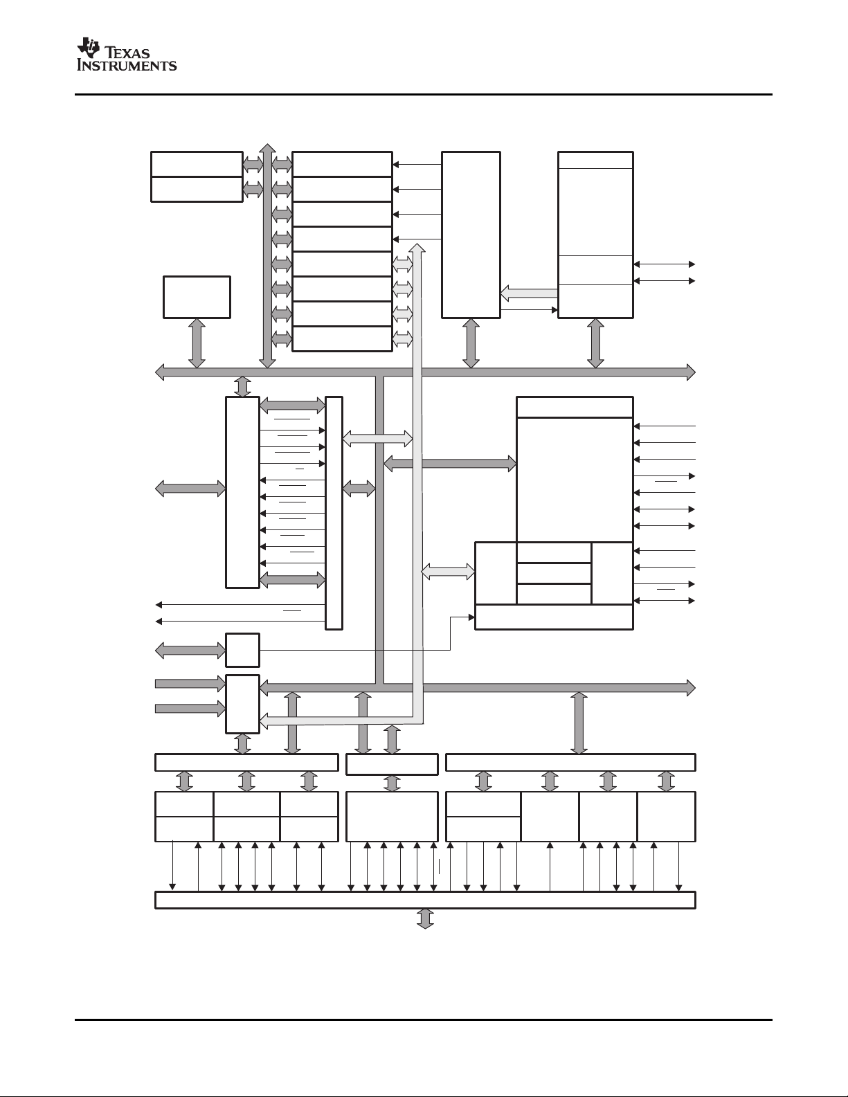
www.ti.com
ADVANCE INFORMATION
3 Functional Overview
M0SARAM1Kx16
(0-Wait)
M1SARAM1Kx16
(0-Wait)
L0SARAM4Kx16
(0-Wait,DualMap)
L1SARAM4Kx16
(0-Wait,DualMap)
L2SARAM4Kx16
(0-Wait,DualMap)
L3SARAM4Kx16
(0-Wait,DualMap)
L4SARAM4Kx16
(0-WData,1-WProg)
L5SARAM4Kx16
(0-WData,1-WProg)
L6SARAM4Kx16
(0-WData,1-WProg)
L7SARAM4Kx16
(0-WData,1-WProg)
MemoryBus
BootROM
8Kx16
Code
Security
Module
DMA Bus
PSWD
OTP 2Kx16
Flash
256Kx16
8Sectors
Pump
Flash
Wrapper
TEST1
TEST2
XINTF
XA0/XWE1
XWE0
XZCS6
XZCS7
XZCS0
XR/W
XREADY
XHOLD
XHOLDA
XD31:0
XA19:1
GPIO
MUX
MemoryBus
MemoryBus
XCLKOUT
XRD
GPIO
MUX
88GPIOs
8ExternalInterrupts
88GPIOs
12-Bit
ADC
2-S/H
A7:0
B7:0
CPUTimer0
CPUTimer1
CPUTimer2
OSC,
PLL,
LPM,
WD
DMA
6Ch
PIE
(Interrupts)
CPU
(150MHZ@1.9V)
EMU1
EMU0
TRST
TDO
TMS
TDI
TCK
XRS
X2
X1
XCLKIN
FPU(F2833xonly)
DMA Bus
MemoryBus
FIFO
(16Levels)
SCI-A/B/C
FIFO
(16Levels)
SPI-A
FIFO
(16Levels)
I2C
16-bitperipheralbus
SPISOMIx
SPISIMOx
SPICLKx
SPISTEx
SCIRXDx
SCITXDx
SDAx
SCLx
McBSP-A/B
MRXx
MDXx
MCLKXx
MCLKRx
MFSXx
MFSRx
32-bitperipheralbus
(DMA accessible)
EPWM-1/../6
HRPWM-1/../6
ECAP-1/../6
EQEP-1/2
EPWMxA
EPWMxB
ESYNCI
ESYNCO
TZx
ECAPx
EQEPxA
EQEPxB
EQEPxI
EQEPxS
CAN-A/B
(32-mbox)
CANRXx
CANTXx
32-bitperipheralbus
GPIOMUX
88GPIOs
TMS320F28335, TMS320F28334, TMS320F28332
TMS320F28235, TMS320F28234, TMS320F28232
Digital Signal Controllers (DSCs)
SPRS439C – JUNE 2007 – REVISED FEBRUARY 2008
Submit Documentation Feedback Functional Overview 35
Figure 3-1. Functional Block Diagram

www.ti.com
ADVANCE INFORMATION
TMS320F28335, TMS320F28334, TMS320F28332
TMS320F28235, TMS320F28234, TMS320F28232
Digital Signal Controllers (DSCs)
SPRS439C – JUNE 2007 – REVISED FEBRUARY 2008
3.1 Memory Maps
In Figure 3-2 through Figure 3-4 , the following apply:
• Memory blocks are not to scale.
• Peripheral Frame 0, Peripheral Frame 1, Peripheral Frame 2, and Peripheral Frame 3 memory maps
are restricted to data memory only. A user program cannot access these memory maps in program
space.
• Protected means the order of "Write followed by Read" operations is preserved rather than the pipeline
order.
• Certain memory ranges are EALLOW protected against spurious writes after configuration.
• Locations 0x38 0080 - 0x38 008F contain the ADC calibration routine. It is not programmable by the
user.
• If the eCAN module is not used in an application, the RAM available (LAM, MOTS, MOTO, and
mailbox RAM) can be used as general-purpose RAM. The CAN module clock should be enabled for
this.
Functional Overview36 Submit Documentation Feedback

www.ti.com
ADVANCE INFORMATION
Block
Start Address
0x000000
M0Vector-RAM(32x32)
(EnableifVMAP =0)
DataSpace
ProgSpace
M0SARAM(1Kx16)
M1SARAM(1Kx16)
PeripheralFrame0
0x000040
0x000400
0x000800
PIEVector-RAM
(256x16)
(Enabledif
VMAP =1,
ENPIE=1)
PeripheralFrame0
Reserved
Reserved
L0SARAM(4Kx16,SecureZoneDualMapped)
PeripheralFrame1
(Protected)
Reserved
PeripheralFrame2
(Protected)
L1SARAM(4Kx16,SecureZoneDualMapped)
FLASH(256Kx16,SecureZone)
Reserved
BootROM(8Kx16)
BROMVector-ROM(32x32)
(EnableifVMAP =1,ENPIE=0)
0x000D00
0x000E00
0x002000
0x006000
0x007000
0x008000
0x009000
0x010000
0x300000
0x3FC000
0x3FE000
0x3FFFC0
DataSpace
ProgSpace
Reserved
Reserved
On-ChipMemory ExternalMemoryXINTF
Onlyoneofthesevectormaps-M0vector,PIEvector,BROMvector-shouldbeenabledatatime.
LEGEND:
L2SARAM(4Kx16,SecureZone,DualMapped)
L3SARAM(4Kx16,SecureZone,DualMapped)
L4SARAM(4Kx16,DMA Accessible)
L5SARAM(4Kx16,DMA Accessible)
L6SARAM(4Kx16,DMA Accessible)
L7SARAM(4Kx16,DMA Accessible)
0x00 A000
0x00B000
0x00C000
0x00D000
0x00E000
0x00F000
Reserved
Reserved
XINTFZone0(4Kx16, )
(Protected,DMA Accessible)
XZCS0
0x004000
0x005000
Low64K
(24x/240xEquivalentDataSpace)
High64K
(24x/240xEquivalent
ProgramSpace)
0x005000
PeripheralFrame3
Protected(DMA Accessible)
128-bitPassword
0x33FFF8
0x340000
L0SARAM(4Kx16,SecureZoneDualMapped)
UserOTP (1Kx16,SecureZone)
0x3F8000
Reserved
0x380400
L1SARAM(4Kx16,SecureZoneDualMapped)
0x3F9000
L2SARAM(4Kx16,SecureZoneDualMapped)
0x3F A000
L3SARAM(4Kx16,SecureZoneDualMapped)
0x3FB000
0x380800
Reserved
XINTFZone6(1Mx16, )(DMA Accessible)XZCS6
0x100000
0x200000
0x300000
XINTFZone7(1Mx16, )XZCS7 (DMA Accessible)
ADCCalibrationData
0x380080
Reserved
0x380090
TMS320F28335, TMS320F28334, TMS320F28332
TMS320F28235, TMS320F28234, TMS320F28232
Digital Signal Controllers (DSCs)
SPRS439C – JUNE 2007 – REVISED FEBRUARY 2008
Submit Documentation Feedback Functional Overview 37
Figure 3-2. F28335/F28235 Memory Map

www.ti.com
ADVANCE INFORMATION
ExternalMemoryXINTF
Block
Start Address
0x000000
M0Vector-RAM(32x32)
(EnableifVMAP =0)
DataSpace
ProgSpace
M0SARAM(1Kx16)
M1SARAM(1Kx16)
PeripheralFrame0
0x000040
0x000400
0x000800
PIEVector-RAM
(256x16)
(Enabledif
VMAP =1,
ENPIE=1)
Reserved
Reserved
L0SARAM(4Kx16,SecureZoneDualMapped)
PeripheralFrame1
(Protected)
Reserved
PeripheralFrame2
(Protected)
L1SARAM(4Kx16,SecureZoneDualMapped)
FLASH(128Kx16,SecureZone)
Reserved
BootROM(8Kx16)
BROMVector-ROM(32x32)
(EnableifVMAP =1,ENPIE=0)
0x000D00
0x000E00
0x002000
0x006000
0x007000
0x008000
0x009000
0x010000
0x320000
0x3FC000
0x3FE000
0x3FFFC0
DataSpace
ProgSpace
Reserved
XINTFZone0(4Kx16, )
(Protected,DMA Accessible)
XZCS0
Reserved
On-ChipMemory
Onlyoneofthesevectormaps-M0vector,PIEvector,BROMvector,-shouldbeenabledatatime.
LEGEND:
L2SARAM(4Kx16,SecureZone,DualMapped)
L3SARAM(4Kx16,SecureZone,DualMapped)
L4SARAM(4Kx16,DMA Accessible)
L5SARAM(4Kx16,DMA Accessible)
L6SARAM(4Kx16,DMA Accessible)
L7SARAM(4Kx16,DMA Accessible)
0x00 A000
0x00B000
0x00C000
0x00D000
0x00E000
0x00F000
Reserved
Reserved
0x004000
0x005000
Low64K
(24x/240xEquivalentDataSpace)
High64K
(24x/240xEquivalent
ProgramSpace)
0x005000
PeripheralFrame3
Protected(DMA Accessible)
128-bitPassword
0x33FFF8
0x340000
L0SARAM(4Kx16,SecureZoneDualMapped)
UserOTP (1Kx16,SecureZone)
0x3F8000
Reserved
0x380400
L1SARAM(4Kx16,SecureZoneDualMapped)
0x3F9000
L2SARAM(4Kx16,SecureZoneDualMapped)
0x3F A000
L3SARAM(4Kx16,SecureZoneDualMapped)
0x3FB000
PeripheralFrame0
XINTFZone6(1Mx16, )(DMA Accessible)XZCS6
0x100000
0x200000
0x300000
XINTFZone7(1Mx16, )XZCS7 (DMA Accessible)
0x380080
ADCCalibrationData
Reserved
0x380800
Reserved
0x380090
TMS320F28335, TMS320F28334, TMS320F28332
TMS320F28235, TMS320F28234, TMS320F28232
Digital Signal Controllers (DSCs)
SPRS439C – JUNE 2007 – REVISED FEBRUARY 2008
Functional Overview38 Submit Documentation Feedback
Figure 3-3. F28334/F28234 Memory Map
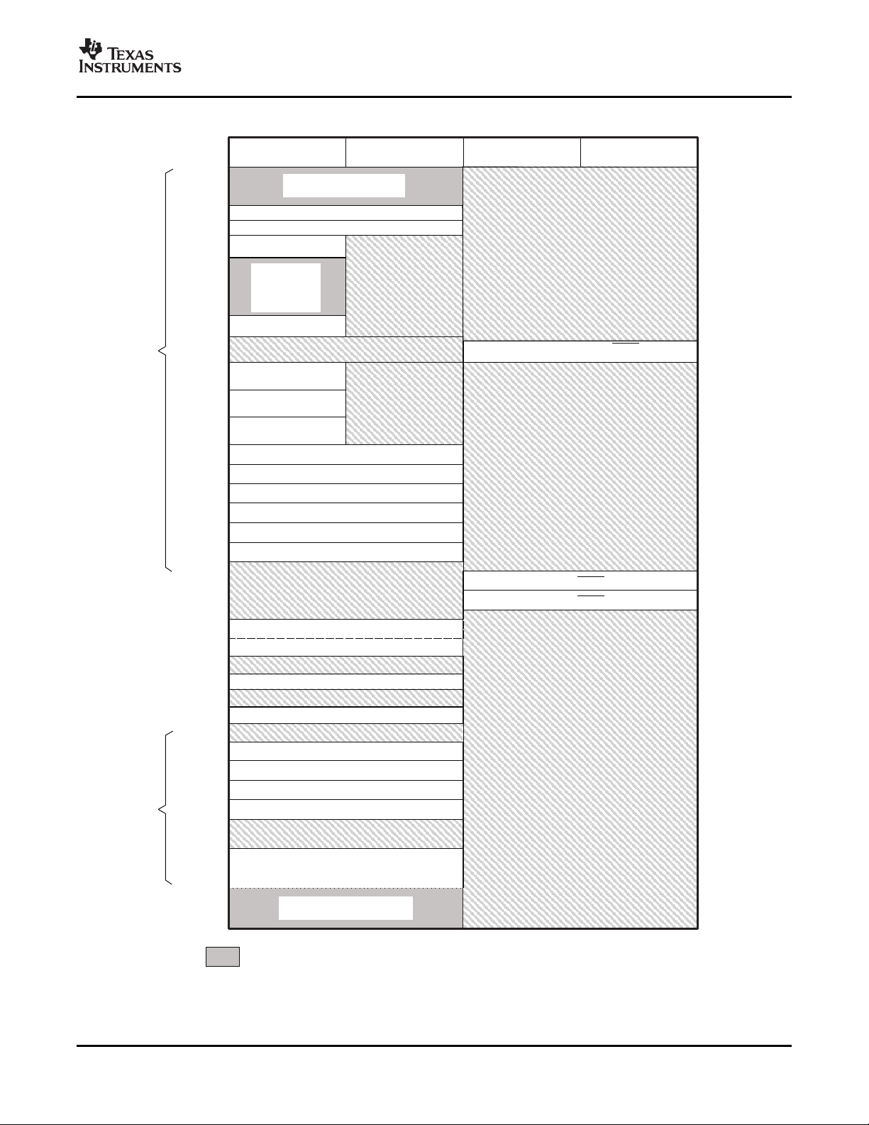
www.ti.com
ADVANCE INFORMATION
Block
Start Address
0x000000
M0Vector-RAM(32x32)
(EnableifVMAP =0)
DataSpace
ProgSpace
M0SARAM(1Kx16)
M1SARAM(1Kx16)
PeripheralFrame0
0x000040
0x000400
0x000800
PIEVector-RAM
(256x16)
(Enabledif
VMAP =1,
ENPIE=1)
Reserved
Reserved
L0SARAM(4Kx16,SecureZoneDualMapped)
PeripheralFrame1
(Protected)
Reserved
PeripheralFrame2
(Protected)
L1SARAM(4Kx16,SecureZoneDualMapped)
FLASH(64Kx16,SecureZone)
Reserved
BootROM(8Kx16)
BROMVector-ROM(32x32)
(EnableifVMAP =1,ENPIE=0)
0x000D00
0x000E00
0x002000
0x006000
0x007000
0x008000
0x009000
0x330000
0x3FC000
0x3FE000
0x3FFFC0
DataSpace
ProgSpace
Reserved
XINTFZone0(4Kx16, )
(Protected,DMA Accessible)
XZCS0
Reserved
On-ChipMemory ExternalMemoryXINTF
Onlyoneofthesevectormaps-M0vector,PIEvector,BROMvector,-shouldbeenabledatatime.
LEGEND:
L2SARAM(4Kx16,SecureZone,DualMapped)
L3SARAM(4Kx16,SecureZone,DualMapped)
L4SARAM(4Kx16,DMA Accessible)
L5SARAM(4Kx16,DMA Accessible)
0x00 A000
0x00B000
0x00C000
0x00D000
0x00E000
Reserved
Reserved
0x004000
0x005000
Low64K
(24x/240xEquivalentDataSpace)
High64K
(24x/240xEquivalent
ProgramSpace)
0x005000
PeripheralFrame3
Protected(DMA Accessible)
128-bitPassword
0x33FFF8
0x340000
L0SARAM(4Kx16,SecureZoneDualMapped)
UserOTP (1Kx16,SecureZone)
0x3F8000
Reserved
0x380400
L1SARAM(4Kx16,SecureZoneDualMapped)
0x3F9000
L2SARAM(4Kx16,SecureZoneDualMapped)
0x3F A000
L3SARAM(4Kx16,SecureZoneDualMapped)
0x3FB000
PeripheralFrame0
XINTFZone6(1Mx16, )(DMA Accessible)XZCS6
0x100000
0x200000
0x300000
XINTFZone7(1Mx16, )XZCS7 (DMA Accessible)
ADCCalibrationData
0x380080
0x380800
Reserved
0x380090
Reserved
TMS320F28335, TMS320F28334, TMS320F28332
TMS320F28235, TMS320F28234, TMS320F28232
Digital Signal Controllers (DSCs)
SPRS439C – JUNE 2007 – REVISED FEBRUARY 2008
Figure 3-4. F28332/F28232 Memory Map
Submit Documentation Feedback Functional Overview 39

www.ti.com
ADVANCE INFORMATION
TMS320F28335, TMS320F28334, TMS320F28332
TMS320F28235, TMS320F28234, TMS320F28232
Digital Signal Controllers (DSCs)
SPRS439C – JUNE 2007 – REVISED FEBRUARY 2008
0x30 0000 - 0x30 7FFF Sector H (32K x 16)
0x30 8000 - 0x30 FFFF Sector G (32K x 16)
0x31 0000 - 0x31 7FFF Sector F (32K x 16)
0x31 8000 - 0x31 FFFF Sector E (32K x 16)
0x32 0000 - 0x32 7FFF Sector D (32K x 16)
0x32 8000 - 0x32 FFFF Sector C (32K x 16)
0x33 0000 - 0x33 7FFF Sector B (32K x 16)
0x33 8000 - 0x33 FF7F Sector A (32K x 16)
0x33 FF80 - 0x33 FFF5
0x33 FFF6 - 0x33 FFF7
0x33 FFF8 - 0x33 FFFF
0x32 0000 - 0x32 3FFF Sector H (16K x 16)
0x32 4000 - 0x32 7FFF Sector G (16K x 16)
0x32 8000 - 0x32 BFFF Sector F (16K x 16)
0x32 C000 - 0x32 FFFF Sector E (16K x 16)
0x33 0000 - 0x33 3FFF Sector D (16K x 16)
0x33 4000 - 0x33 7FFFF Sector C (16K x 16)
0x33 8000 - 0x33 BFFF Sector B (16K x 16)
0x33 C000 - 0x33 FF7F Sector A (16K x 16)
0x33 FF80 - 0x33 FFF5 Program to 0x0000 when using the
0x33 FFF6 - 0x33 FFF7 Boot-to-Flash Entry Point
0x33 FFF8 - 0x33 FFFF Security Password (128-Bit)
Table 3-1. Addresses of Flash Sectors in F28335/F28235
ADDRESS RANGE PROGRAM AND DATA SPACE
Program to 0x0000 when using the
Code Security Module
Boot-to-Flash Entry Point
(program branch instruction here)
Security Password
(128-Bit) (Do Not Program to all zeros)
Table 3-2. Addresses of Flash Sectors in F28334/F28234
ADDRESS RANGE PROGRAM AND DATA SPACE
Code Security Module
(program branch instruction here)
(Do Not Program to all zeros)
Table 3-3. Addresses of Flash Sectors in F28332/F28232
ADDRESS RANGE PROGRAM AND DATA SPACE
0x33 0000 - 0x33 3FFF Sector D (16K x 16)
0x33 4000 - 0x33 7FFFF Sector C (16K x 16)
0x33 8000 - 0x33 BFFF Sector B (16K x 16)
0x33 C000 - 0x33 FF7F Sector A (16K x 16)
0x33 FF80 - 0x33 FFF5 Program to 0x0000 when using the Code Security
Module
0x33 FFF6 - 0x33 FFF7 Boot-to-Flash Entry Point (program branch
instruction here)
0x33 FFF8 - 0x33 FFFF Security Password (128-Bit) (Do Not Program to all
zeros)
Functional Overview40 Submit Documentation Feedback
www.ti.com
ADVANCE INFORMATION
TMS320F28335, TMS320F28334, TMS320F28332
TMS320F28235, TMS320F28234, TMS320F28232
Digital Signal Controllers (DSCs)
SPRS439C – JUNE 2007 – REVISED FEBRUARY 2008
NOTE
• When the code-security passwords are programmed, all addresses between
0x33FF80 and 0x33FFF5 cannot be used as program code or data. These locations
must be programmed to 0x0000.
• If the code security feature is not used, addresses 0x33FF80 through 0x33FFEF may
be used for code or data. Addresses 0x33FFF0 – 0x33FFF5 are reserved for data and
should not contain program code. .
Table 3-4 shows how to handle these memory locations.
Table 3-4. Handling Security Code Locations
ADDRESS FLASH
Code security enabled Code security disabled
0x33FF80 - 0x33FFEF Application code and data
0x33FFF0 - 0x33FFF5 Reserved for data only
Peripheral Frame 1, Peripheral Frame 2, and Peripheral Frame 3 are grouped together to enable these
blocks to be write/read peripheral block protected. The protected mode ensures that all accesses to these
blocks happen as written. Because of the C28x pipeline, a write immediately followed by a read, to
different memory locations, will appear in reverse order on the memory bus of the CPU. This can cause
problems in certain peripheral applications where the user expected the write to occur first (as written).
The C28x CPU supports a block protection mode where a region of memory can be protected so as to
make sure that operations occur as written (the penalty is extra cycles are added to align the operations).
This mode is programmable and by default, it will protect the selected zones.
Fill with 0x0000
The wait-states for the various spaces in the memory map area are listed in Table 3-5 .
Submit Documentation Feedback Functional Overview 41

www.ti.com
ADVANCE INFORMATION
TMS320F28335, TMS320F28334, TMS320F28332
TMS320F28235, TMS320F28234, TMS320F28232
Digital Signal Controllers (DSCs)
SPRS439C – JUNE 2007 – REVISED FEBRUARY 2008
Table 3-5. Wait-states
Area Wait-States (CPU) Wait-States (DMA)
M0 and M1 SARAMs 0-wait Fixed
Peripheral Frame 0 0-wait (writes) 0-wait (reads)
1-wait (reads)
Peripheral Frame 3 0-wait (writes) 0-wait (writes) Assumes no conflicts between CPU and DMA.
2-wait (reads) 1-wait (reads)
Peripheral Frame 1 0-wait (writes) Cycles can be extended by peripheral generated ready.
2-wait (reads) Consecutive writes to the CAN will experience a 1-cycle
Peripheral Frame 2 0-wait (writes) Fixed. Cycles cannot be extended by the peripheral.
2-wait (reads)
L0 SARAM 0-wait data and Assumes no CPU conflicts
L1 SARAM
L2 SARAM
L3 SARAM
L4 SARAM 0-wait data (read) 0-wait data (write) Assumes no conflicts between CPU and DMA.
L5 SARAM 0-wait data (write) 0-wait data (read)
L6 SARAM 1-wait program (read)
L7 SARAM 1-wait program (write)
XINTF Programmable Programmed via the XTIMING registers or extendable via
OTP Programmable Programmed via the Flash registers.
FLASH Programmable Programmed via the Flash registers.
FLASH Password Wait states of password locations are fixed.
Boot-ROM 1-wait 0-wait speed is not possible.
(1) The DMA has a base of 4 cycles/word.
program
1-wait minimum 1-wait is minimum wait states allowed on external waveforms
0-wait minimum writes 0-wait data (write) 0-wait minimum for writes assumes write buffer enabled and
with write buffer 0-wait data (read) not full.
enabled Assumes no conflicts between CPU and DMA. When DMA
1-wait minimum 1-wait is minimum number of wait states allowed. 1-wait-state
1-wait Paged min 0-wait minimum for paged access is not allowed
1-wait Random min 1-wait-state operation is possible at a reduced CPU
Random ≥ Paged frequency.
16-wait fixed
3.2 Brief Descriptions
(1)
Comments
pipeline hit.
external XREADY signal.
for both reads and writes on XINTF.
and CPU attempt simultaneous conflict, 1-cycle delay is
added for arbitration.
operation is possible at a reduced CPU frequency.
3.2.1 C28x CPU
The F2833x (C28x+FPU) family is a member of the TMS320C2000™ digital signal controller (DSC)
platform. The C28x+FPU based controllers have the same 32-bit fixed-point architecture as TI's existing
C28x DSCs, but also include a single-precision (32-bit) IEEE 754 floating-point unit (FPU). It is a very
efficient C/C++ engine, hence enabling users to develop not only their system control software in a
high-level language, but also enables math algorithms to be developed using C/C++. The device is as
efficient in DSP math tasks as it is in system control tasks that typically are handled by microcontroller
devices. This efficiency removes the need for a second processor in many systems. The 32 x 32-bit MAC
capabilities of the F2833x and its 64-bit processing capabilities, enable it to efficiently handle higher
numerical resolution problems. Add to this the fast interrupt response with automatic context save of
Functional Overview42 Submit Documentation Feedback

www.ti.com
ADVANCE INFORMATION
TMS320F28335, TMS320F28334, TMS320F28332
TMS320F28235, TMS320F28234, TMS320F28232
Digital Signal Controllers (DSCs)
SPRS439C – JUNE 2007 – REVISED FEBRUARY 2008
critical registers, resulting in a device that is capable of servicing many asynchronous events with minimal
latency. The device has an 8-level-deep protected pipeline with pipelined memory accesses. This
pipelining enables it to execute at high speeds without resorting to expensive high-speed memories.
Special branch-look-ahead hardware minimizes the latency for conditional discontinuities. Special store
conditional operations further improve performance.
The F2823x family is also a member of the TMS320C2000™ digital signal controller (DSC) platform but it
does not include a floating-point unit (FPU).
3.2.2 Memory Bus (Harvard Bus Architecture)
As with many DSC type devices, multiple busses are used to move data between the memories and
peripherals and the CPU. The C28x memory bus architecture contains a program read bus, data read bus
and data write bus. The program read bus consists of 22 address lines and 32 data lines. The data read
and write busses consist of 32 address lines and 32 data lines each. The 32-bit-wide data busses enable
single cycle 32-bit operations. The multiple bus architecture, commonly termed Harvard Bus, enables the
C28x to fetch an instruction, read a data value and write a data value in a single cycle. All peripherals and
memories attached to the memory bus will prioritize memory accesses. Generally, the priority of memory
bus accesses can be summarized as follows:
Highest: Data Writes (Simultaneous data and program writes cannot occur on the memory bus.)
Program Writes (Simultaneous data and program writes cannot occur on the memory bus.)
Data Reads
Program Reads (Simultaneous program reads and fetches cannot occur on the memory bus.)
Lowest: Fetches (Simultaneous program reads and fetches cannot occur on the memory bus.)
3.2.3 Peripheral Bus
To enable migration of peripherals between various Texas Instruments (TI) DSC family of devices, the
F2833x/F2823x devices adopt a peripheral bus standard for peripheral interconnect. The peripheral bus
bridge multiplexes the various busses that make up the processor Memory Bus into a single bus
consisting of 16 address lines and 16 or 32 data lines and associated control signals. Three versions of
the peripheral bus are supported. One version supports only 16-bit accesses (called peripheral frame 2).
Another version supports both 16- and 32-bit accesses (called peripheral frame 1). The third version
supports DMA access and both 16- and 32-bit accesses (called peripheral frame 3).
3.2.4 Real-Time JTAG and Analysis
The F2833x/F2823x devices implement the standard IEEE 1149.1 JTAG interface. Additionally, the
devices support real-time mode of operation whereby the contents of memory, peripheral and register
locations can be modified while the processor is running and executing code and servicing interrupts. The
user can also single step through non-time critical code while enabling time-critical interrupts to be
serviced without interference. The device implements the real-time mode in hardware within the CPU. This
is a feature unique to the F2833x/F2823x device, requiring no software monitor. Additionally, special
analysis hardware is provided that allows setting of hardware breakpoint or data/address watch-points and
generate various user-selectable break events when a match occurs.
3.2.5 External Interface (XINTF)
This asynchronous interface consists of 20 address lines, 32 data lines, and three chip-select lines. The
chip-select lines are mapped to three external zones, Zones 0, 6, and 7. Each of the three zones can be
programmed with a different number of wait states, strobe signal setup and hold timing and each zone can
be programmed for extending wait states externally or not. The programmable wait-state, chip-select and
programmable strobe timing enables glueless interface to external memories and peripherals.
Submit Documentation Feedback Functional Overview 43

www.ti.com
ADVANCE INFORMATION
TMS320F28335, TMS320F28334, TMS320F28332
TMS320F28235, TMS320F28234, TMS320F28232
Digital Signal Controllers (DSCs)
SPRS439C – JUNE 2007 – REVISED FEBRUARY 2008
3.2.6 Flash
The F28335/F28235 devices contain 256K × 16 of embedded flash memory, segregated into eight 32K ×
16 sectors. The F28334/F28234 devices contain 128K × 16 of embedded flash memory, segregated into
eight 16K × 16 sectors. The F28332/F28232 devices contain 64K × 16 of embedded flash, segregated into
four 16K × 16 sectors. All the devices also contain a single 1K × 16 of OTP memory at address range
0x380400 – 0x3807FF. The user can individually erase, program, and validate a flash sector while leaving
other sectors untouched. However, it is not possible to use one sector of the flash or the OTP to execute
flash algorithms that erase/program other sectors. Special memory pipelining is provided to enable the
flash module to achieve higher performance. The flash/OTP is mapped to both program and data space;
therefore, it can be used to execute code or store data information. Note that addresses 0x33FFF0 –
0x33FFF5 are reserved for data variables and should not contain program code.
The Flash and OTP wait-states can be configured by the application. This allows
applications running at slower frequencies to configure the flash to use fewer wait-states.
Flash effective performance can be improved by enabling the flash pipeline mode in the
Flash options register. With this mode enabled, effective performance of linear code
execution will be much faster than the raw performance indicated by the wait-state
configuration alone. The exact performance gain when using the Flash pipeline mode is
application-dependent.
For more information on the Flash options, Flash wait-state, and OTP wait-state registers,
see the TMS320F2833x Digital Signal Controller (DSC) System Control and Interrupts
Reference Guide (literature number SPRUFB0 ).
NOTE
3.2.7 M0, M1 SARAMs
All F2833x/F2823x devices contain these two blocks of single access memory, each 1K × 16 in size. The
stack pointer points to the beginning of block M1 on reset. The M0 and M1 blocks, like all other memory
blocks on C28x devices, are mapped to both program and data space. Hence, the user can use M0 and
M1 to execute code or for data variables. The partitioning is performed within the linker. The C28x device
presents a unified memory map to the programmer. This makes for easier programming in high-level
languages.
3.2.8 L0, L1, L2, L3, L4, L5, L6, L7 SARAMs
The F28335/F28235 and F28334/F28234 each contain an additional 32K × 16 of single-access RAM,
divided into 8 blocks (L0-L7 with 4K each). The F28332/F28232 contain an additional 24K × 16 of
single-access RAM, divided into 6 blocks (L0-L5 with 4K each). Each block can be independently
accessed to minimize CPU pipeline stalls. Each block is mapped to both program and data space. L4, L5,
L6, and L7 are DMA accessible
3.2.9 Boot ROM
The Boot ROM is factory-programmed with boot-loading software. Boot-mode signals are provided to tell
the bootloader software what boot mode to use on power up. The user can select to boot normally or to
download new software from an external connection or to select boot software that is programmed in the
internal Flash/ROM. The Boot ROM also contains standard tables, such as SIN/COS waveforms, for use
in math related algorithms.
Functional Overview44 Submit Documentation Feedback

www.ti.com
ADVANCE INFORMATION
TMS320F28335, TMS320F28334, TMS320F28332
TMS320F28235, TMS320F28234, TMS320F28232
Digital Signal Controllers (DSCs)
SPRS439C – JUNE 2007 – REVISED FEBRUARY 2008
Table 3-6. Boot Mode Selection
MODE GPIO87/XA15 GPIO86/XA14 GPIO85/XA13 GPIO84/XA12 MODE
F 1 1 1 1 Jump to Flash
E 1 1 1 0 SCI-A boot
D 1 1 0 1 SPI-A boot
C 1 1 0 0 I2C-A boot
B 1 0 1 1 eCAN-A boot
A 1 0 1 0 McBSP-A boot
9 1 0 0 1 Jump to XINTF x16
8 1 0 0 0 Jump to XINTF x32
7 0 1 1 1 Jumpto OTP
6 0 1 1 0 Parallel GPIO I/O boot
5 0 1 0 1 Parallel XINTF boot
4 0 1 0 0 Jump to SARAM
3 0 0 1 1 Branch to check boot mode
2 0 0 1 0 Branch to Flash, skip ADC calibration
1 0 0 0 1 Branch to SARAM, skip ADC
calibration
0 0 0 0 0 Branch to SCI, skip ADC calibration
(1) All four GPIO pins have an internal pullup.
(1)
NOTE
Modes 0, 1, and 2 in Table 3-6 are for TI debug only. Skipping the ADC calibration
function in an application will cause the ADC to operate outside of the stated
specifications
3.2.10 Security
The devices support high levels of security to protect the user firmware from being reverse engineered.
The security features a 128-bit password (hardcoded for 16 wait-states), which the user programs into the
flash. One code security module (CSM) is used to protect the flash/OTP and the L0/L1/L2/L3 SARAM
blocks. The security feature prevents unauthorized users from examining the memory contents via the
JTAG port, executing code from external memory or trying to boot-load some undesirable software that
would export the secure memory contents. To enable access to the secure blocks, the user must write the
correct 128-bit KEY value, which matches the value stored in the password locations within the Flash.
In addition to the CSM, the emulation code security logic (ECSL) has been implemented to prevent
unauthorized users from stepping through secure code. Any code or data access to flash, user OTP, L0,
L1, L2 or L3 memory while the emulator is connected will trip the ECSL and break the emulation
connection. To allow emulation of secure code, while maintaining the CSM protection against secure
memory reads, the user must write the correct value into the lower 64 bits of the KEY register, which
matches the value stored in the lower 64 bits of the password locations within the flash. Note that dummy
reads of all 128 bits of the password in the flash must still be performed. If the lower 64 bits of the
password locations are all ones (unprogrammed), then the KEY value does not need to match.
When initially debugging a device with the password locations in flash programmed (i.e., secured), the
emulator takes some time to take control of the CPU. During this time, the CPU will start running and may
execute an instruction that performs an access to a protected ECSL area. If this happens, the ECSL will
trip and cause the emulator connection to be cut. Two solutions to this problem exist:
1. The first is to use the Wait-In-Reset emulation mode, which will hold the device in reset until the
emulator takes control. The emulator must support this mode for this option.
2. The second option is to use the “Branch to check boot mode” boot option. This will sit in a loop and
continuously poll the boot mode select pins. The user can select this boot mode and then exit this
Submit Documentation Feedback Functional Overview 45

www.ti.com
ADVANCE INFORMATION
TMS320F28335, TMS320F28334, TMS320F28332
TMS320F28235, TMS320F28234, TMS320F28232
Digital Signal Controllers (DSCs)
SPRS439C – JUNE 2007 – REVISED FEBRUARY 2008
mode once the emulator is connected by re-mapping the PC to another address or by changing the
boot mode selection pin to the desired boot mode.
• When the code-security passwords are programmed, all addresses between
0x33FF80 and 0x33FFF5 cannot be used as program code or data. These locations
must be programmed to 0x0000.
• If the code security feature is not used, addresses 0x33FF80 through 0x33FFEF may
be used for code or data. Addresses 0x33FFF0 – 0x33FFF5 are reserved for data and
should not contain program code. .
The 128-bit password (at 0x33 FFF8 – 0x33 FFFF) must not be programmed to zeros.
Doing so would permanently lock the device.
Code Security Module Disclaimer
THE CODE SECURITY MODULE (CSM) INCLUDED ON THIS DEVICE WAS
DESIGNED TO PASSWORD PROTECT THE DATA STORED IN THE ASSOCIATED
MEMORY (EITHER ROM OR FLASH) AND IS WARRANTED BY TEXAS
INSTRUMENTS (TI), IN ACCORDANCE WITH ITS STANDARD TERMS AND
CONDITIONS, TO CONFORM TO TI'S PUBLISHED SPECIFICATIONS FOR THE
WARRANTY PERIOD APPLICABLE FOR THIS DEVICE.
TI DOES NOT, HOWEVER, WARRANT OR REPRESENT THAT THE CSM CANNOT BE
COMPROMISED OR BREACHED OR THAT THE DATA STORED IN THE ASSOCIATED
MEMORY CANNOT BE ACCESSED THROUGH OTHER MEANS. MOREOVER,
EXCEPT AS SET FORTH ABOVE, TI MAKES NO WARRANTIES OR
REPRESENTATIONS CONCERNING THE CSM OR OPERATION OF THIS DEVICE,
INCLUDING ANY IMPLIED WARRANTIES OF MERCHANTABILITY OR FITNESS FOR
A PARTICULAR PURPOSE.
IN NO EVENT SHALL TI BE LIABLE FOR ANY CONSEQUENTIAL, SPECIAL,
INDIRECT, INCIDENTAL, OR PUNITIVE DAMAGES, HOWEVER CAUSED, ARISING IN
ANY WAY OUT OF YOUR USE OF THE CSM OR THIS DEVICE, WHETHER OR NOT
TI HAS BEEN ADVISED OF THE POSSIBILITY OF SUCH DAMAGES. EXCLUDED
DAMAGES INCLUDE, BUT ARE NOT LIMITED TO LOSS OF DATA, LOSS OF
GOODWILL, LOSS OF USE OR INTERRUPTION OF BUSINESS OR OTHER
ECONOMIC LOSS.
NOTE
disclaimer
3.2.11 Peripheral Interrupt Expansion (PIE) Block
The PIE block serves to multiplex numerous interrupt sources into a smaller set of interrupt inputs. The
PIE block can support up to 96 peripheral interrupts. On the F2833x/F2823x, 58 of the possible 96
interrupts are used by peripherals. The 96 interrupts are grouped into blocks of 8 and each group is fed
into 1 of 12 CPU interrupt lines (INT1 to INT12). Each of the 96 interrupts is supported by its own vector
stored in a dedicated RAM block that can be overwritten by the user. The vector is automatically fetched
by the CPU on servicing the interrupt. It takes 8 CPU clock cycles to fetch the vector and save critical
CPU registers. Hence the CPU can quickly respond to interrupt events. Prioritization of interrupts is
controlled in hardware and software. Each individual interrupt can be enabled/disabled within the PIE
block.
Functional Overview46 Submit Documentation Feedback

www.ti.com
ADVANCE INFORMATION
3.2.12 External Interrupts (XINT1-XINT7, XNMI)
The devices support eight masked external interrupts (XINT1-XINT7, XNMI). XNMI can be connected to
the INT13 or NMI interrupt of the CPU. Each of the interrupts can be selected for negative, positive, or
both negative and positive edge triggering and can also be enabled/disabled (including the XNMI). XINT1,
XINT2, and XNMI also contain a 16-bit free running up counter, which is reset to zero when a valid
interrupt edge is detected. This counter can be used to accurately time stamp the interrupt. Unlike the
281x devices, there are no dedicated pins for the external interrupts. XINT1 XINT2, and XNMI interrupts
can accept inputs from GPIO0 – GPIO31 pins. XINT3 – XINT7 interrupts can accept inputs from GPIO32
– GPIO63 pins.
3.2.13 Oscillator and PLL
The device can be clocked by an external oscillator or by a crystal attached to the on-chip oscillator circuit.
A PLL is provided supporting up to 10 input-clock-scaling ratios. The PLL ratios can be changed on-the-fly
in software, enabling the user to scale back on operating frequency if lower power operation is desired.
Refer to the Electrical Specification section for timing details. The PLL block can be set in bypass mode.
3.2.14 Watchdog
The devices contain a watchdog timer. The user software must regularly reset the watchdog counter
within a certain time frame; otherwise, the watchdog will generate a reset to the processor. The watchdog
can be disabled if necessary.
TMS320F28335, TMS320F28334, TMS320F28332
TMS320F28235, TMS320F28234, TMS320F28232
Digital Signal Controllers (DSCs)
SPRS439C – JUNE 2007 – REVISED FEBRUARY 2008
3.2.15 Peripheral Clocking
The clocks to each individual peripheral can be enabled/disabled so as to reduce power consumption
when a peripheral is not in use. Additionally, the system clock to the serial ports (except I2C and eCAN)
and the ADC blocks can be scaled relative to the CPU clock. This enables the timing of peripherals to be
decoupled from increasing CPU clock speeds.
3.2.16 Low-Power Modes
The devices are full static CMOS devices. Three low-power modes are provided:
IDLE: Place CPU into low-power mode. Peripheral clocks may be turned off selectively and only
those peripherals that need to function during IDLE are left operating. An enabled interrupt
from an active peripheral or the watchdog timer will wake the processor from IDLE mode.
STANDBY: Turns off clock to CPU and peripherals. This mode leaves the oscillator and PLL functional.
An external interrupt event will wake the processor and the peripherals. Execution begins
on the next valid cycle after detection of the interrupt event
HALT: Turns off the internal oscillator. This mode basically shuts down the device and places it in
the lowest possible power consumption mode. A reset or external signal can wake the
device from this mode.
3.2.17 Peripheral Frames 0, 1, 2, 3 (PFn)
The device segregates peripherals into three sections. The mapping of peripherals is as follows:
PF0: PIE: PIE Interrupt Enable and Control Registers Plus PIE Vector Table
Flash: Flash Waitstate Registers
XINTF: External Interface Registers
DMA DMA Registers
Timers: CPU-Timers 0, 1, 2 Registers
CSM: Code Security Module KEY Registers
ADC: ADC Result Registers (dual-mapped)
Submit Documentation Feedback Functional Overview 47

www.ti.com
ADVANCE INFORMATION
TMS320F28335, TMS320F28334, TMS320F28332
TMS320F28235, TMS320F28234, TMS320F28232
Digital Signal Controllers (DSCs)
SPRS439C – JUNE 2007 – REVISED FEBRUARY 2008
PF1: eCAN: eCAN Mailbox and Control Registers
GPIO: GPIO MUX Configuration and Control Registers
ePWM: Enhanced Pulse Width Modulator Module and Registers
eCAP: Enhanced Capture Module and Registers
eQEP: Enhanced Quadrature Encoder Pulse Module and Registers
PF2: SYS: System Control Registers
SCI: Serial Communications Interface (SCI) Control and RX/TX Registers
SPI: Serial Port Interface (SPI) Control and RX/TX Registers
ADC: ADC Status, Control, and Result Register
I2C: Inter-Integrated Circuit Module and Registers
XINT External Interrupt Registers
PF3: McBSP Multichannel Buffered Serial Port Registers
3.2.18 General-Purpose Input/Output (GPIO) Multiplexer
Most of the peripheral signals are multiplexed with general-purpose input/output (GPIO) signals. This
enables the user to use a pin as GPIO if the peripheral signal or function is not used. On reset, GPIO pins
are configured as inputs. The user can individually program each pin for GPIO mode or peripheral signal
mode. For specific inputs, the user can also select the number of input qualification cycles. This is to filter
unwanted noise glitches. The GPIO signals can also be used to bring the device out of specific low-power
modes.
3.2.19 32-Bit CPU-Timers (0, 1, 2)
CPU-Timers 0, 1, and 2 are identical 32-bit timers with presettable periods and with 16-bit clock
prescaling. The timers have a 32-bit count down register, which generates an interrupt when the counter
reaches zero. The counter is decremented at the CPU clock speed divided by the prescale value setting.
When the counter reaches zero, it is automatically reloaded with a 32-bit period value. CPU-Timer 2 is
reserved for Real-Time OS (RTOS)/BIOS applications. It is connected to INT14 of the CPU. If DSP/BIOS
is not being used, CPU-Timer 2 is available for general use. CPU-Timer 1 is for general use and can be
connected to INT13 of the CPU. CPU-Timer 0 is also for general use and is connected to the PIE block.
3.2.20 Control Peripherals
The F2833x/F2823x devices support the following peripherals which are used for embedded control and
communication:
ePWM: The enhanced PWM peripheral supports independent/complementary PWM generation,
adjustable dead-band generation for leading/trailing edges, latched/cycle-by-cycle trip
mechanism. Some of the PWM pins support HRPWM features.
eCAP: The enhanced capture peripheral uses a 32-bit time base and registers up to four
programmable events in continuous/one-shot capture modes.
This peripheral can also be configured to generate an auxiliary PWM signal.
eQEP: The enhanced QEP peripheral uses a 32-bit position counter, supports low-speed
measurement using capture unit and high-speed measurement using a 32-bit unit timer.
This peripheral has a watchdog timer to detect motor stall and input error detection logic
to identify simultaneous edge transition in QEP signals.
ADC: The ADC block is a 12-bit converter, single ended, 16-channels. It contains two
sample-and-hold units for simultaneous sampling.
3.2.21 Serial Port Peripherals
48 Functional Overview Submit Documentation Feedback

www.ti.com
ADVANCE INFORMATION
TMS320F28335, TMS320F28334, TMS320F28332
TMS320F28235, TMS320F28234, TMS320F28232
Digital Signal Controllers (DSCs)
SPRS439C – JUNE 2007 – REVISED FEBRUARY 2008
The devices support the following serial communication peripherals:
eCAN: This is the enhanced version of the CAN peripheral. It supports 32 mailboxes, time
stamping of messages, and is CAN 2.0B-compliant.
McBSP: The multichannel buffered serial port (McBSP) connects to E1/T1 lines, phone-quality
codecs for modem applications or high-quality stereo audio DAC devices. The McBSP
receive and transmit registers are supported by the DMA to significantly reduce the
overhead for servicing this peripheral. Each McBSP module can be configured as an SPI
as required.
SPI: The SPI is a high-speed, synchronous serial I/O port that allows a serial bit stream of
programmed length (one to sixteen bits) to be shifted into and out of the device at a
programmable bit-transfer rate. Normally, the SPI is used for communications between the
DSC and external peripherals or another processor. Typical applications include external
I/O or peripheral expansion through devices such as shift registers, display drivers, and
ADCs. Multi-device communications are supported by the master/slave operation of the
SPI. On the F2833x/F2823x, the SPI contains a 16-level receive and transmit FIFO for
reducing interrupt servicing overhead.
SCI: The serial communications interface is a two-wire asynchronous serial port, commonly
known as UART. The SCI contains a 16-level receive and transmit FIFO for reducing
interrupt servicing overhead.
I2C: The inter-integrated circuit (I2C) module provides an interface between a DSC and other
devices compliant with Philips Semiconductors Inter-IC bus (I2C-bus) specification version
2.1 and connected by way of an I2C-bus. External components attached to this 2-wire
serial bus can transmit/receive up to 8-bit data to/from the DSC through the I2C module.
On the F2833x/F2823x, the I2C contains a 16-level receive and transmit FIFO for
reducing interrupt servicing overhead.
3.3 Register Map
The devices contain four peripheral register spaces. The spaces are categorized as follows:
Peripheral These are peripherals that are mapped directly to the CPU memory bus.
Frame 0: See Table 3-7
Peripheral These are peripherals that are mapped to the 32-bit peripheral bus.
Frame 1 See Table 3-8
Peripheral These are peripherals that are mapped to the 16-bit peripheral bus.
Frame 2: See Table 3-9
Peripheral These are peripherals that are mapped to the 32-bit DMA-accessible peripheral
Frame 3: bus.
See Table 3-10
Table 3-7. Peripheral Frame 0 Registers
NAME ADDRESS RANGE SIZE ( × 16) ACCESS TYPE
Device Emulation Registers 0x00 0880 - 0x00 09FF 384 EALLOW protected
FLASH Registers
Code Security Module Registers 0x00 0AE0 - 0x00 0AEF 16 EALLOW protected
ADC registers (dual-mapped) 0x00 0B00 - 0x00 0B0F 16 Not EALLOW protected
0 wait (DMA), 1 wait (CPU), read only
XINTF Registers 0x00 0B20 - 0x00 0B3F 32 Not EALLOW protected
(1) Registers in Frame 0 support 16-bit and 32-bit accesses.
(2) If registers are EALLOW protected, then writes cannot be performed until the EALLOW instruction is executed. The EDIS instruction
disables writes to prevent stray code or pointers from corrupting register contents.
(3) The Flash Registers are also protected by the Code Security Module (CSM).
(3)
0x00 0A80 - 0x00 0ADF 96 EALLOW protected
(1)
(2)
Submit Documentation Feedback Functional Overview 49
www.ti.com
ADVANCE INFORMATION
TMS320F28335, TMS320F28334, TMS320F28332
TMS320F28235, TMS320F28234, TMS320F28232
Digital Signal Controllers (DSCs)
SPRS439C – JUNE 2007 – REVISED FEBRUARY 2008
Table 3-7. Peripheral Frame 0 Registers (continued)
NAME ADDRESS RANGE SIZE ( × 16) ACCESS TYPE
CPU–TIMER0/1/2 Registers 0x00 0C00 - 0x00 0C3F 64 Not EALLOW protected
PIE Registers 0x00 0CE0 - 0x00 0CFF 32 Not EALLOW protected
PIE Vector Table 0x00 0D00 - 0x00 0DFF 256 EALLOW protected
DMA Registers 0x00 1000 - 0x00 11FF 512 EALLOW protected
Table 3-8. Peripheral Frame 1 Registers
NAME ADDRESS RANGE SIZE ( × 16)
ECAN-A Registers 0x0000 6000 - 0x0000 61FF 512
ECAN-B Registers 0x0000 6200 - 0x0000 63FF 512
EPWM1 + HRPWM1 Registers 0x0000 6800 - 0x0000 683F 64
EPWM2 + HRPWM2 Registers 0x0000 6840 - 0x0000 687F 64
EPWM3 + HRPWM3 Registers 0x0000 6880 - 0x0000 68BF 64
EPWM4 + HRPWM4 Registers 0x0000 68C0 - 0x0000 68FF 64
EPWM5 + HRPWM5 Registers 0x0000 6900 - 0x0000 693F 64
EPWM6 + HRPWM6 Registers 0x0000 6940 - 0x0000 697F 64
ECAP1 Registers 0x0000 6A00 - 0x0000 6A1F 32
ECAP2 Registers 0x0000 6A20 - 0x0000 6A3F 32
ECAP3 Registers 0x0000 6A40 - 0x0000 6A5F 32
ECAP4 Registers 0x0000 6A60 - 0x0000 6A7F 32
ECAP5 Registers 0x0000 6A80 - 0x0000 6A9F 32
ECAP6 Registers 0x0000 6AA0 - 0x0000 6ABF 32
EQEP1 Registers 0x0000 6B00 - 0x0000 6B3F 64
EQEP2 Registers 0x0000 6B40 - 0x0000 6B7F 64
GPIO Registers 0x0000 6F80 - 0x0000 6FFF 128
(2)
Table 3-9. Peripheral Frame 2 Registers
NAME ADDRESS RANGE SIZE ( × 16)
System Control Registers 0x0000 7010 - 0x0000 702F 32
SPI-A Registers 0x0000 7040 - 0x0000 704F 16
SCI-A Registers 0x0000 7050 - 0x0000 705F 16
External Interrupt Registers 0x0000 7070 - 0x0000 707F 16
ADC Registers 0x0000 7100 - 0x0000 711F 32
SCI-B Registers 0x0000 7750 - 0x0000 775F 16
SCI-C Registers 0x0000 7770 - 0x0000 777F 16
I2C-A Registers 0x0000 7900 - 0x0000 793F 64
Table 3-10. Peripheral Frame 3 Registers
NAME ADDRESS RANGE SIZE ( × 16)
McBSP-A Registers 0x0000 5000 - 0x0000 503F 64
McBSP-B Registers 0x0000 5040 - 0x0000 507F 64
3.4 Device Emulation Registers
These registers are used to control the protection mode of the C28x CPU and to monitor some critical
device signals. The registers are defined in Table 3-11 .
Functional Overview50 Submit Documentation Feedback

www.ti.com
ADVANCE INFORMATION
TMS320F28335, TMS320F28334, TMS320F28332
TMS320F28235, TMS320F28234, TMS320F28232
Digital Signal Controllers (DSCs)
SPRS439C – JUNE 2007 – REVISED FEBRUARY 2008
Table 3-11. Device Emulation Registers
NAME SIZE (x16) DESCRIPTION
DEVICECNF 2 Device Configuration Register
PARTID 0x0882 1 Part ID Register 0x00F8
REVID 0x0883 1 Revision ID Register 0x0000 - Silicon Rev. 0 - TMX
PROTSTART 0x0884 1 Block Protection Start Address Register
PROTRANGE 0x0885 1 Block Protection Range Address Register
(1) The first byte (00) denotes flash devices. FF denotes ROM devices. Other values are reserved for future devices.
ADDRESS
RANGE
0x0880
0x0881
(1)
0x00F9 - F28334/F28234
0x00FA - F28335/F28235
- F28332/F28232
Submit Documentation Feedback Functional Overview 51
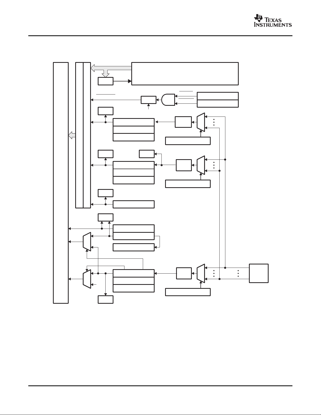
www.ti.com
ADVANCE INFORMATION
WDINT
LPMINT
Watchdog
LowPowerModels
Sync
SYSCLKOUT
WAKEINT
DMA
Clear
Peripherals
(SPI,SCI,I2C,CAN,McBSP
C )
(A),
(A)
EPWM,ECAP,EQEP, AD
DMA
XINT1
InterruptControl
XINT1CR(15:0)
XINT1CTR(15:0)
XINT1
Latch
MUX
GPIOXINT1SEL(4:0)
DMA
XINT2
InterruptControl
XINT2CR(15:0)
XINT2CTR(15:0)
XINT2
Latch
MUX
GPIOXINT2SEL(4:0)
ADC
XINT2SOC
DMA
TINT0
CPUTimer0
DMA
TINT2
CPUTimer2
CPUTimer1
MUX
TINT1
FlashWrapper
TOUT1
InterruptControl
XNMICR(15:0)
XNMICTR(15:0)
MUX
1
DMA
NMI
INT13
INT14
INT1
to
INT12
C28
Core
96Interrupts
PIE
XNMI_
XINT13
Latch
MUX
GPIOXNMISEL(4:0)
GPIO
Mux
GPIO0.int
GPIO31.int
TMS320F28335, TMS320F28334, TMS320F28332
TMS320F28235, TMS320F28234, TMS320F28232
Digital Signal Controllers (DSCs)
SPRS439C – JUNE 2007 – REVISED FEBRUARY 2008
3.5 Interrupts
Figure 3-5 shows how the various interrupt sources are multiplexed.
A. DMA-accessible
Figure 3-5. External and PIE Interrupt Sources
Functional Overview52 Submit Documentation Feedback

www.ti.com
ADVANCE INFORMATION
InterruptControl
XINT3CR(15:0)
Latch
Mux
GPIOXINT3SEL(4:0)
DMA
XINT3
InterruptControl
XINT4CR(15:0)
Latch
Mux
GPIOXINT4SEL(4:0)
XINT4
InterruptControl
XINT5CR(15:0)
Mux
GPIOXINT5SEL(4:0)
XINT5
InterruptControl
XINT6CR(15:0)
Mux
GPIOXINT6SEL(4:0)
XINT6
InterruptControl
XINT7CR(15:0)
Mux
GPIOXINT7SEL(4:0)
XINT7
DMA
DMA
DMA
DMA
96Interrupts
PIE
INT1
to
INT12
C28
Core
GPIO32.int
GPIO63.int
GPIO
Mux
Latch
Latch
Latch
TMS320F28335, TMS320F28334, TMS320F28332
TMS320F28235, TMS320F28234, TMS320F28232
Digital Signal Controllers (DSCs)
SPRS439C – JUNE 2007 – REVISED FEBRUARY 2008
Figure 3-6. External Interrupts
Eight PIE block interrupts are grouped into one CPU interrupt. In total, 12 CPU interrupt groups, with 8
interrupts per group equals 96 possible interrupts. On the F2833x/F2823x, 58 of these are used by
peripherals as shown in Table 3-12 .
The TRAP #VectorNumber instruction transfers program control to the interrupt service routine
corresponding to the vector specified. TRAP #0 attempts to transfer program control to the address
pointed to by the reset vector. The PIE vector table does not, however, include a reset vector. Therefore,
TRAP #0 should not be used when the PIE is enabled. Doing so will result in undefined behavior.
When the PIE is enabled, TRAP #1 through TRAP #12 will transfer program control to the interrupt service
routine corresponding to the first vector within the PIE group. For example: TRAP #1 fetches the vector
from INT1.1, TRAP #2 fetches the vector from INT2.1, and so forth.
Submit Documentation Feedback Functional Overview 53

www.ti.com
ADVANCE INFORMATION
INT12
MUX
INT11
INT2
INT1
CPU
(Enable)(Flag)
INTx
INTx.8
PIEIERx(8:1) PIEIFRx(8:1)
MUX
INTx.7
INTx.6
INTx.5
INTx.4
INTx.3
INTx.2
INTx.1
From
Peripherals or
External
Interrupts
(Enable) (Flag)
IER(12:1)IFR(12:1)
Global
Enable
INTM
1
0
PIEACKx
(Enable/Flag)
TMS320F28335, TMS320F28334, TMS320F28332
TMS320F28235, TMS320F28234, TMS320F28232
Digital Signal Controllers (DSCs)
SPRS439C – JUNE 2007 – REVISED FEBRUARY 2008
Figure 3-7. Multiplexing of Interrupts Using the PIE Block
Table 3-12. PIE Peripheral Interrupts
CPU
INTERRUPTS
INT1 XINT2 XINT1 Reserved
INT2 Reserved Reserved
INT3 Reserved Reserved
INT4 Reserved Reserved
INT5 Reserved Reserved Reserved Reserved Reserved Reserved
INT6 Reserved Reserved
INT7 Reserved Reserved
INT8 Reserved Reserved Reserved Reserved
INT9
INT10 Reserved Reserved Reserved Reserved Reserved Reserved Reserved Reserved
INT11 Reserved Reserved Reserved Reserved Reserved Reserved Reserved Reserved
INT12 Reserved XINT7 XINT6 XINT5 XINT4 XINT3
INTx.8 INTx.7 INTx.6 INTx.5 INTx.4 INTx.3 INTx.2 INTx.1
WAKEINT TINT0 ADCINT SEQ2INT SEQ1INT
(LPM/WD) (TIMER 0) (ADC) (ADC) (ADC)
EPWM6_TZINT EPWM5_TZINT EPWM4_TZINT EPWM3_TZINT EPWM2_TZINT EPWM1_TZINT
(ePWM6) (ePWM5) (ePWM4) (ePWM3) (ePWM2) (ePWM1)
EPWM6_INT EPWM5_INT EPWM4_INT EPWM3_INT EPWM2_INT EPWM1_INT
(ePWM6) (ePWM5) (ePWM4) (ePWM3) (ePWM2) (ePWM1)
ECAP6_INT ECAP5_INT ECAP4_INT ECAP3_INT ECAP2_INT ECAP1_INT
(ECAP6) (ECAP5) (eCAP4) (eCAP3) (eCAP2) (eCAP1)
MXINTA MRINTA MXINTB MRINTB SPITXINTA SPIRXINTA
(McBSP-A) (McBSP-A) (McBSP-B) (McBSP-B) (SPI-A) (SPI-A)
DINTCH6 DINTCH5 DINTCH4 DINTCH3 DINTCH2 DINTCH1
(DMA) (DMA) (DMA) (DMA) (DMA) (DMA)
SCITXINTC SCIRXINTC I2CINT2A I2CINT1A
(SCI-C) (SCI-C) (I2C-A) (I2C-A)
ECAN1_INTB ECAN0_INTB ECAN1_INTA ECAN0_INTA SCITXINTB SCIRXINTB SCITXINTA SCIRXINTA
(CAN-B) (CAN-B) (CAN-A) (CAN-A) (SCI-B) (SCI-B) (SCI-A) (SCI-A)
LUF LVF
(FPU) (FPU)
(1) Out of the 96 possible interrupts, 58 interrupts are currently used. The remaining interrupts are reserved for future devices. These
interrupts can be used as software interrupts if they are enabled at the PIEIFRx level, provided none of the interrupts within the group is
being used by a peripheral. Otherwise, interrupts coming in from peripherals may be lost by accidentally clearing their flag while
modifying the PIEIFR. To summarize, there are two safe cases when the reserved interrupts could be used as software interrupts:
1) No peripheral within the group is asserting interrupts.
2) No peripheral interrupts are assigned to the group (example PIE group 11).
Functional Overview54 Submit Documentation Feedback
PIE INTERRUPTS
(1)
EQEP2_INT EQEP1_INT
(eQEP2) (eQEP1)
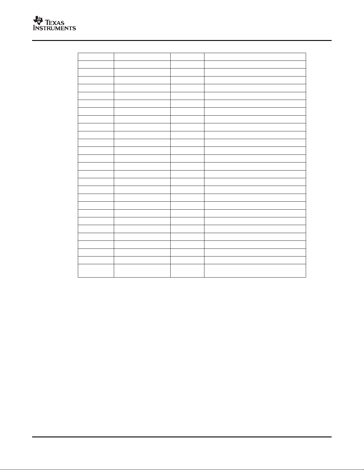
www.ti.com
ADVANCE INFORMATION
TMS320F28335, TMS320F28334, TMS320F28332
TMS320F28235, TMS320F28234, TMS320F28232
Digital Signal Controllers (DSCs)
SPRS439C – JUNE 2007 – REVISED FEBRUARY 2008
Table 3-13. PIE Configuration and Control Registers
NAME ADDRESS SIZE (X16) DESCRIPTION
PIECTRL 0x0CE0 1 PIE, Control Register
PIEACK 0x0CE1 1 PIE, Acknowledge Register
PIEIER1 0x0CE2 1 PIE, INT1 Group Enable Register
PIEIFR1 0x0CE3 1 PIE, INT1 Group Flag Register
PIEIER2 0x0CE4 1 PIE, INT2 Group Enable Register
PIEIFR2 0x0CE5 1 PIE, INT2 Group Flag Register
PIEIER3 0x0CE6 1 PIE, INT3 Group Enable Register
PIEIFR3 0x0CE7 1 PIE, INT3 Group Flag Register
PIEIER4 0x0CE8 1 PIE, INT4 Group Enable Register
PIEIFR4 0x0CE9 1 PIE, INT4 Group Flag Register
PIEIER5 0x0CEA 1 PIE, INT5 Group Enable Register
PIEIFR5 0x0CEB 1 PIE, INT5 Group Flag Register
PIEIER6 0x0CEC 1 PIE, INT6 Group Enable Register
PIEIFR6 0x0CED 1 PIE, INT6 Group Flag Register
PIEIER7 0x0CEE 1 PIE, INT7 Group Enable Register
PIEIFR7 0x0CEF 1 PIE, INT7 Group Flag Register
PIEIER8 0x0CF0 1 PIE, INT8 Group Enable Register
PIEIFR8 0x0CF1 1 PIE, INT8 Group Flag Register
PIEIER9 0x0CF2 1 PIE, INT9 Group Enable Register
PIEIFR9 0x0CF3 1 PIE, INT9 Group Flag Register
PIEIER10 0x0CF4 1 PIE, INT10 Group Enable Register
PIEIFR10 0x0CF5 1 PIE, INT10 Group Flag Register
PIEIER11 0x0CF6 1 PIE, INT11 Group Enable Register
PIEIFR11 0x0CF7 1 PIE, INT11 Group Flag Register
PIEIER12 0x0CF8 1 PIE, INT12 Group Enable Register
PIEIFR12 0x0CF9 1 PIE, INT12 Group Flag Register
Reserved 0x0CFA 6 Reserved
0x0CFF
(1) The PIE configuration and control registers are not protected by EALLOW mode. The PIE vector table
is protected.
(1)
Submit Documentation Feedback Functional Overview 55

www.ti.com
ADVANCE INFORMATION
TMS320F28335, TMS320F28334, TMS320F28332
TMS320F28235, TMS320F28234, TMS320F28232
Digital Signal Controllers (DSCs)
SPRS439C – JUNE 2007 – REVISED FEBRUARY 2008
3.5.1 External Interrupts
Name Address Size (x16) Description
XINT1CR 0x0000 7070 1 XINT1 configuration register
XINT2CR 0x0000 7071 1 XINT2 configuration register
XINT3CR 0x0000 7072 1 XINT3 configuration register
XINT4CR 0x0000 7073 1 XINT4 configuration register
XINT5CR 0x0000 7074 1 XINT5 configuration register
XINT6CR 0x0000 7075 1 XINT6 configuration register
XINT7CR 0x0000 7076 1 XINT7 configuration register
XNMICR 0x0000 7077 1 XNMI configuration register
XINT1CTR 0x0000 7078 1 XINT1 counter register
XINT2CTR 0x0000 7079 1 XINT2 counter register
Reserved 0x707A - 0x707E 5
XNMICTR 0x0000 707F 1 XNMI counter register
Each external interrupt can be enabled/disabled or qualified using positive, negative, or both positive and
negative edge. For more information, see the TMS320F2833x Digital Signal Controller (DSC) System and
Interrupts Reference Guide (literature number SPRUFB0 ).
Table 3-14. External Interrupt Registers
3.6 System Control
This section describes the oscillator, PLL and clocking mechanisms, the watchdog function and the low
power modes. Figure 3-8 shows the various clock and reset domains that will be discussed.
Functional Overview56 Submit Documentation Feedback

www.ti.com
ADVANCE INFORMATION
EPWM1/../6,HRPWM1/../6,
ECAP1/../6,EQEP1/2
Peripheral
registers
Bridge
Clockenables
I/O
Peripheral
registers
Clockenables
I/O
eCAN-A/B
/2
Peripheral
registers
Clockenables
I/O
SPI-A,SCI-A/B/C,I2C-A
LOSPCP
LSPCLK
System
control
register
Bridge
SYSCLKOUT
Memorybus
C28xCore
GPIO
Mux
Clockenable
Peripheral
registers
I/O
McBSP-A/B
LOSPCP
LSPCLK
Clockenables
Bridge
HISPCP
HSPCLK
DMA
bus
Result
registers
Bridge
12-Bit ADC
ADC
registers
16channels
DMA
ClockEnables
Peripheralbus
CPUtimer
registers
CPUtimer0/1/2
Clockenable
TMS320F28335, TMS320F28334, TMS320F28332
TMS320F28235, TMS320F28234, TMS320F28232
Digital Signal Controllers (DSCs)
SPRS439C – JUNE 2007 – REVISED FEBRUARY 2008
A. CLKIN is the clock into the CPU. It is passed out of the CPU as SYSCLKOUT (that is, CLKIN is the same frequency
as SYSCLKOUT). See Figure 3-9 for an illustration of how CLKIN is derived.
Figure 3-8. Clock and Reset Domains
Submit Documentation Feedback Functional Overview 57
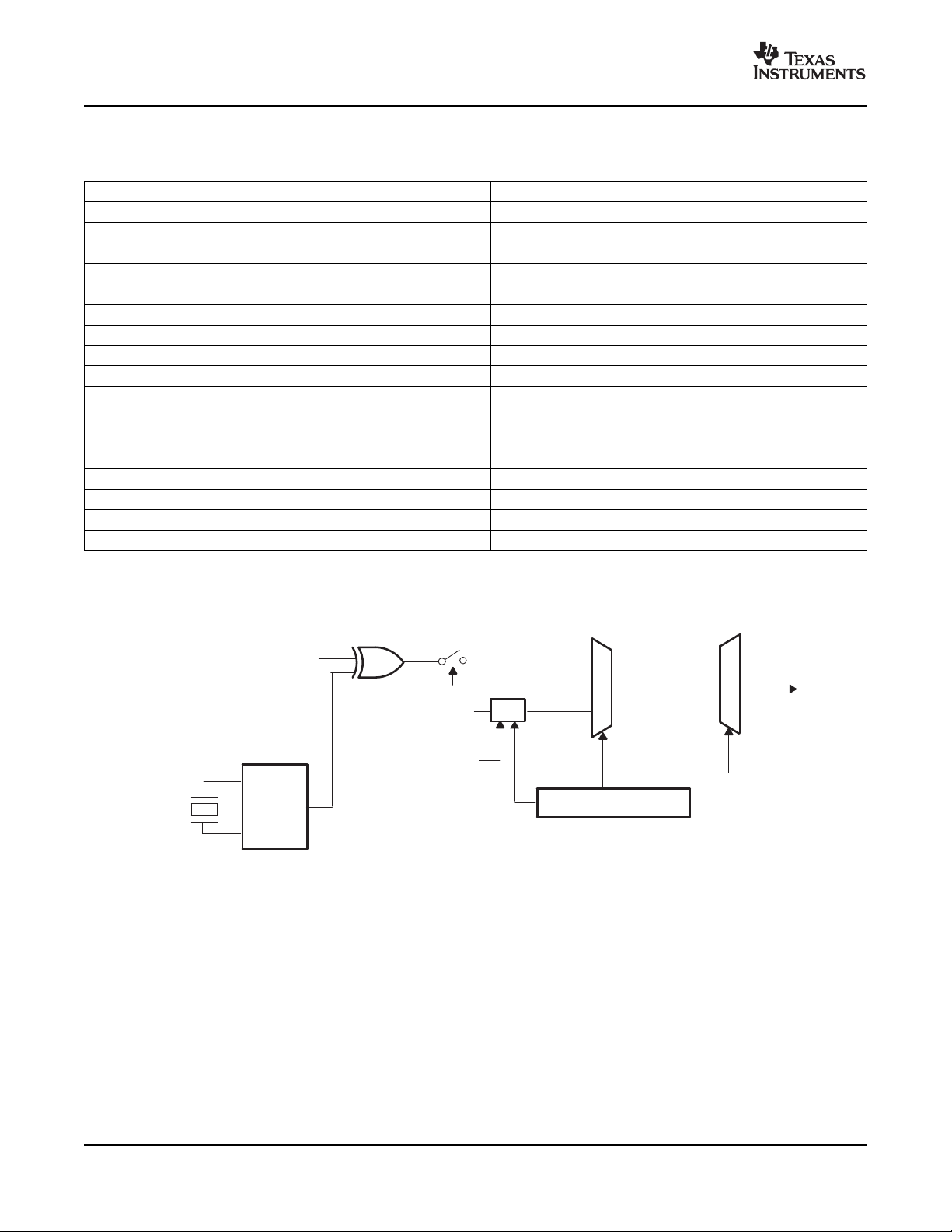
www.ti.com
ADVANCE INFORMATION
X1
XCLKIN
(3.3-Vclockinput
fromexternal
oscillator)
On-chip
oscillator
X2
PLLSTS[OSCOFF]
OSCCLK
PLL
VCOCLK
4-bitPLL Select(PLLCR)
OSCCLKor
VCOCLK
CLKIN
OSCCLK
0
PLLSTS[PLLOFF]
n
n
≠ 0
PLLSTS[DIVSEL]
/1
/2
/4
External
Crystalor
Resonator
To
CPU
TMS320F28335, TMS320F28334, TMS320F28332
TMS320F28235, TMS320F28234, TMS320F28232
Digital Signal Controllers (DSCs)
SPRS439C – JUNE 2007 – REVISED FEBRUARY 2008
The PLL, clocking, watchdog and low-power modes, are controlled by the registers listed in Table 3-15 .
Table 3-15. PLL, Clocking, Watchdog, and Low-Power Mode Registers
Name Address Size (x16) Description
PLLSTS 0x0000-7011 1 PLL Status Register
Reserved 0x0000-7012 - 0x0000-7018 7
HISPCP 0x0000-701A 1 High-Speed Peripheral Clock Pre-Scaler Register
LOSPCP 0x0000-701B 1 Low-Speed Peripheral Clock Pre-Scaler Register
PCLKCR0 0x0000-701C 1 Peripheral Clock Control Register 0
PCLKCR1 0x0000-701D 1 Peripheral Clock Control Register 1
LPMCR0 0x0000-701E 1 Low Power Mode Control Register 0
Reserved 0x0000-701F 1 Low Power Mode Control Register 1
PCLKCR3 0x0000-7020 1 Peripheral Clock Control Register 3
PLLCR 0x0000-7021 1 PLL Control Register
SCSR 0x0000-7022 1 System Control and Status Register
WDCNTR 0x0000-7023 1 Watchdog Counter Register
Reserved 0x0000-7024 1
WDKEY 0x0000-7025 1 Watchdog Reset Key Register
Reserved 0x0000-7026 - 0x0000-7028 3
WDCR 0x0000-7029 1 Watchdog Control Register
Reserved 0x0000-702A - 0x0000-702F 6
3.6.1 OSC and PLL Block
Figure 3-9 shows the OSC and PLL block.
The on-chip oscillator circuit enables a crystal/resonator to be attached to the F2833x/F2823x devices
using the X1 and X2 pins. If the on-chip oscillator is not used, an external oscillator can be used in either
one of the following configurations:
1. A 3.3-V external oscillator can be directly connected to the XCLKIN pin. The X2 pin should be left
unconnected and the X1 pin tied low. The logic-high level in this case should not exceed V
2. A 1.9-V external oscillator can be directly connected to the X1 pin. The X2 pin should be left
unconnected and the XCLKIN pin tied low. The logic-high level in this case should not exceed V
The three possible input-clock configurations are shown in Figure 3-10 through Figure 3-12
Figure 3-9. OSC and PLL Block Diagram
.
DDIO
.
DD
Functional Overview58 Submit Documentation Feedback
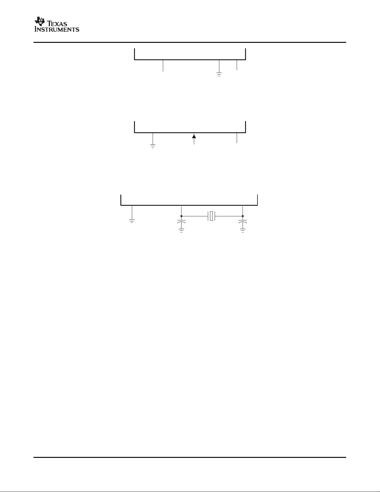
www.ti.com
ADVANCE INFORMATION
External Clock Signal
(Toggling 0−V
DDIO
)
XCLKIN
X2
NC
X1
External Clock Signal
(Toggling 0−VDD)
XCLKIN
X2
NC
X1
C
L1
X2X1
Crystal
C
L2
XCLKIN
Figure 3-10. Using a 3.3-V External Oscillator
Figure 3-11. Using a 1.9-V External Oscillator
TMS320F28335, TMS320F28334, TMS320F28332
TMS320F28235, TMS320F28234, TMS320F28232
Digital Signal Controllers (DSCs)
SPRS439C – JUNE 2007 – REVISED FEBRUARY 2008
Figure 3-12. Using the Internal Oscillator
3.6.1.1 External Reference Oscillator Clock Option
The typical specifications for the external quartz crystal for a frequency of 20 MHz are listed below:
• Fundamental mode, parallel resonant
• C
(load capacitance) = 12 pF
L
• C
• C
= C
L1
shunt
= 24 pF
L2
= 6 pF
• ESR range = 30 to 60 Ω
TI recommends that customers have the resonator/crystal vendor characterize the operation of their
device with the DSC chip. The resonator/crystal vendor has the equipment and expertise to tune the tank
circuit. The vendor can also advise the customer regarding the proper tank component values that will
produce proper start up and stability over the entire operating range.
3.6.1.2 PLL-Based Clock Module
The devices have an on-chip, PLL-based clock module. This module provides all the necessary clocking
signals for the device, as well as control for low-power mode entry. The PLL has a 4-bit ratio control
PLLCR[DIV] to select different CPU clock rates. The watchdog module should be disabled before writing
to the PLLCR register. It can be re-enabled (if need be) after the PLL module has stabilized, which takes
131072 OSCCLK cycles. The input clock and PLLCR[DIV] bits should be chosen in such a way that the
output frequency of the PLL (VCOCLK) does not exceed 300 MHz.
Submit Documentation Feedback Functional Overview 59

www.ti.com
ADVANCE INFORMATION
TMS320F28335, TMS320F28334, TMS320F28332
TMS320F28235, TMS320F28234, TMS320F28232
Digital Signal Controllers (DSCs)
SPRS439C – JUNE 2007 – REVISED FEBRUARY 2008
Table 3-16. PLLCR
PLLCR[DIV] VALUE
0000 (PLL bypass) OSCCLK/4 (Default) OSCCLK/2 OSCCLK
0001 (OSCCLK * 1)/4 (OSCCLK*1)/2 OSCCLK*1
0010 (OSCCLK * 2)/4 (OSCCLK*2)/2 OSCCLK*2
0011 (OSCCLK * 3)/4 (OSCCLK*3)/2 OSCCLK*3
0100 (OSCCLK * 4)/4 (OSCCLK*4)/2 OSCCLK*4
0101 (OSCCLK * 5)/4 (OSCCLK*5)/2 OSCCLK*5
0110 (OSCCLK * 6)/4 (OSCCLK*6)/2 OSCCLK*6
0111 (OSCCLK * 7)/4 (OSCCLK*7)/2 OSCCLK*7
1000 (OSCCLK * 8)/4 (OSCCLK*8)/2 OSCCLK*8
1001 (OSCCLK * 9)/4 (OSCCLK*9)/2 OSCCLK*9
1010 (OSCCLK * 10)/4 (OSCCLK*10)/2 OSCCLK*10
1011 - 1111 Reserved Reserved Reserved
(1) PLLSTS[DIVSEL] must be 0 before writing to the PLLCR and must be set only to 2 or 3 after PLLSTS[PLLLOCKS] = 1. By default,
PLLSTS[DIVSEL] is configured for /4. The boot ROM changes this to /2.
(2) The PLL control register (PLLCR) and PLL Status Register (PLLSTS) are reset to their default state by the XRS signal or a watchdog
reset only. A reset issued by the debugger or the missing clock detect logic have no effect.
(2)
PLLSTS[DIVSEL] = 0 or 1 PLLSTS[DIVSEL] = 2 PLLSTS[DIVSEL] = 3
(1)
Bit Descriptions
SYSCLKOUT (CLKIN)
Table 3-17. CLKIN Divide Options
PLLSTS [DIVSEL] CLKIN DIVIDE
0 /4
1 /4
2 /2
3 /1
The PLL-based clock module provides two modes of operation:
• Crystal-operation - This mode allows the use of an external crystal/resonator to provide the time base
to the device.
• External clock source operation - This mode allows the internal oscillator to be bypassed. The device
clocks are generated from an external clock source input on the X1 or the XCLKIN pin.
Table 3-18. Possible PLL Configuration Modes
PLL MODE REMARKS PLLSTS[DIVSEL]
Invoked by the user setting the PLLOFF bit in the PLLSTS register. The PLL block
PLL Off power operation. The PLLCR register must first be set to 0x0000 (PLL Bypass) 2 OSCCLK/2
PLL Bypass 2 OSCCLK/2
PLL Enable 2 OSCCLK*n/2
(1) PLLSTS[DIVSEL] must be 0 before writing to the PLLCR and must only be set to 1 after PLLSTS[PLLLOCKS] = 1. See the
TMS320F2833x Digital Signal Controller (DSC) System Control and Interrupts Reference Guide (literature Number SPRUFB0 ) for more
information.
is disabled in this mode. This can be useful to reduce system noise and for low 0, 1 OSCCLK/4
before entering this mode. The CPU clock (CLKIN) is derived directly from the 3 OSCCLK/1
input clock on either X1/X2, X1 or XCLKIN.
PLL Bypass is the default PLL configuration upon power-up or after an external
reset ( XRS). This mode is selected when the PLLCR register is set to 0x0000 or
while the PLL locks to a new frequency after the PLLCR register has been
modified. In this mode, the PLL itself is bypassed but the PLL is not turned off.
Achieved by writing a non-zero value n into the PLLCR register. Upon writing to the
PLLCR the device will switch to PLL Bypass mode until the PLL locks.
0, 1 OSCCLK/4
3 OSCCLK/1
0, 1 OSCCLK*n/4
3 OSCCLK*n/1
(1)
CLKIN AND
SYSCLKOUT
Functional Overview60 Submit Documentation Feedback

www.ti.com
ADVANCE INFORMATION
/512
OSCCLK
WDCR(WDPS[2:0])
WDCLK
WDCNTR(7:0)
WDKEY(7:0)
GoodKey
1 0 1
WDCR(WDCHK[2:0])
Bad
WDCHK
Key
WDCR(WDDIS)
ClearCounter
SCSR(WDENINT)
Watchdog
Prescaler
Generate
OutputPulse
(512OSCCLKs)
8-Bit
Watchdog
Counter
CLR
WDRST
WDINT
Watchdog
55+AA
KeyDetector
XRS
Core-reset
WDRST
(A)
Internal
Pullup
TMS320F28335, TMS320F28334, TMS320F28332
TMS320F28235, TMS320F28234, TMS320F28232
Digital Signal Controllers (DSCs)
SPRS439C – JUNE 2007 – REVISED FEBRUARY 2008
3.6.1.3 Loss of Input Clock
In PLL-enabled and PLL-bypass mode, if the input clock OSCCLK is removed or absent, the PLL will still
issue a limp-mode clock. The limp-mode clock continues to clock the CPU and peripherals at a typical
frequency of 1-5 MHz. Limp mode is not specified to work from power-up, only after input clocks have
been present initially. In PLL bypass mode, the limp mode clock from the PLL is automatically routed to
the CPU if the input clock is removed or absent.
Normally, when the input clocks are present, the watchdog counter decrements to initiate a watchdog
reset or WDINT interrupt. However, when the external input clock fails, the watchdog counter stops
decrementing (i.e., the watchdog counter does not change with the limp-mode clock). In addition to this,
the device will be reset and the “Missing Clock Status” (MCLKSTS) bit will be set. These conditions could
be used by the application firmware to detect the input clock failure and initiate necessary shut-down
procedure for the system.
NOTE
Applications in which the correct CPU operating frequency is absolutely critical should
implement a mechanism by which the DSC will be held in reset, should the input clocks
ever fail. For example, an R-C circuit may be used to trigger the XRS pin of the DSC,
should the capacitor ever get fully charged. An I/O pin may be used to discharge the
capacitor on a periodic basis to prevent it from getting fully charged. Such a circuit would
also help in detecting failure of the flash memory and the V
rail.
DD3VFL
3.6.2 Watchdog Block
The watchdog block on the F2833x/F2823x device is similar to the one used on the 240x and 281x
devices. The watchdog module generates an output pulse, 512 oscillator clocks wide (OSCCLK),
whenever the 8-bit watchdog up counter has reached its maximum value. To prevent this, the user
disables the counter or the software must periodically write a 0x55 + 0xAA sequence into the watchdog
key register which will reset the watchdog counter. Figure 3-13 shows the various functional blocks within
the watchdog module.
A. The WDRST signal is driven low for 512 OSCCLK cycles.
Figure 3-13. Watchdog Module
The WDINT signal enables the watchdog to be used as a wakeup from IDLE/STANDBY mode.
Submit Documentation Feedback Functional Overview 61
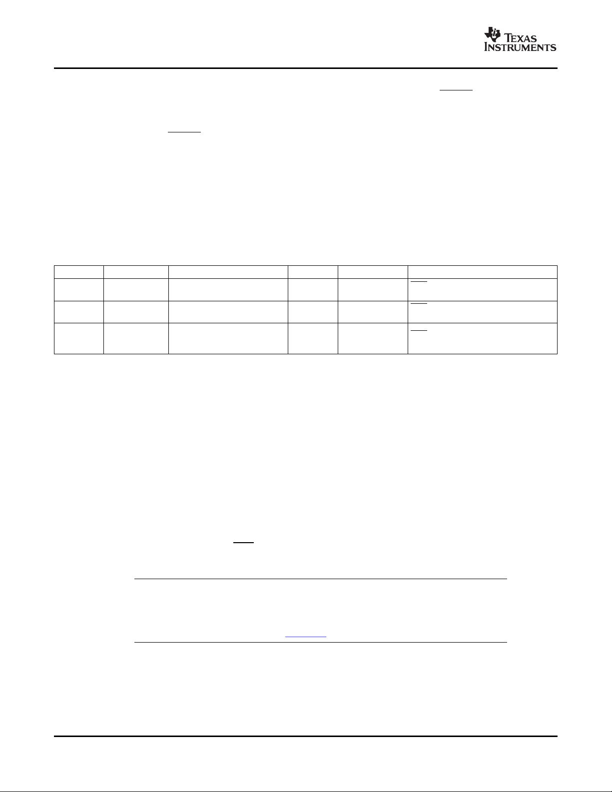
www.ti.com
ADVANCE INFORMATION
TMS320F28335, TMS320F28334, TMS320F28332
TMS320F28235, TMS320F28234, TMS320F28232
Digital Signal Controllers (DSCs)
SPRS439C – JUNE 2007 – REVISED FEBRUARY 2008
In STANDBY mode, all peripherals are turned off on the device. The only peripheral that remains
functional is the watchdog. The WATCHDOG module will run off OSCCLK. The WDINT signal is fed to the
LPM block so that it can wake the device from STANDBY (if enabled). See Section Section 3.7 ,
Low-Power Modes Block, for more details.
In IDLE mode, the WDINT signal can generate an interrupt to the CPU, via the PIE, to take the CPU out of
IDLE mode.
In HALT mode, this feature cannot be used because the oscillator (and PLL) are turned off and hence so
is the WATCHDOG.
3.7 Low-Power Modes Block
The low-power modes on the F2833x/F2823x devices are similar to the 240x devices. Table 3-19
summarizes the various modes.
Table 3-19. Low-Power Modes
MODE LPMCR0(1:0) OSCCLK CLKIN SYSCLKOUT EXIT
IDLE 00 On On On
STANDBY 01 Off Off
HALT 1X (oscillator and PLL turned off, Off Off
(1) The Exit column lists which signals or under what conditions the low power mode will be exited. A low signal, on any of the signals, will
exit the low power condition. This signal must be kept low long enough for an interrupt to be recognized by the device. Otherwise the
IDLE mode will not be exited and the device will go back into the indicated low power mode.
(2) The IDLE mode on the C28x behaves differently than on the 24x/240x. On the C28x, the clock output from the CPU (SYSCLKOUT) is
still functional while on the 24x/240x the clock is turned off.
(3) On the C28x, the JTAG port can still function even if the CPU clock (CLKIN) is turned off.
(watchdog still running) signal, debugger
watchdog not functional)
On XRS, Watchdog interrupt, GPIO Port A
Off
(2)
XRS, Watchdog interrupt, any enabled
interrupt, XNMI
XRS, GPIO Port A signal, XNMI,
debugger
(3)
(1)
(3)
, XNMI
The various low-power modes operate as follows:
IDLE Mode: This mode is exited by any enabled interrupt or an XNMI that is recognized by
the processor. The LPM block performs no tasks during this mode as long as the
LPMCR0(LPM) bits are set to 0,0.
STANDBY Mode: Any GPIO port A signal (GPIO[31:0]) can wake the device from STANDBY
mode. The user must select which signal(s) will wake the device in the
GPIOLPMSEL register. The selected signal(s) are also qualified by the OSCCLK
before waking the device. The number of OSCCLKs is specified in the LPMCR0
register.
HALT Mode: Only the XRS and any GPIO port A signal (GPIO[31:0]) can wake the device
from HALT mode. The user selects the signal in the GPIOLPMSEL register.
NOTE
The low-power modes do not affect the state of the output pins (PWM pins included).
They will be in whatever state the code left them in when the IDLE instruction was
executed. See the TMS320F2833x Digital Signal Controller (DSC) System and Interrupts
Reference Guide (literature number SPRUFB0 ) for more details.
62 Functional Overview Submit Documentation Feedback

www.ti.com
ADVANCE INFORMATION
TMS320F28335, TMS320F28334, TMS320F28332
TMS320F28235, TMS320F28234, TMS320F28232
Digital Signal Controllers (DSCs)
SPRS439C – JUNE 2007 – REVISED FEBRUARY 2008
4 Peripherals
The integrated peripherals of the F2833x/F2823x devices are described in the following subsections:
• 6-channel Direct Memory Access (DMA)
• Three 32-bit CPU-Timers
• Up to six enhanced PWM modules (ePWM1, ePWM2, ePWM3, ePWM4, ePWM5, ePWM6)
• Up to six enhanced capture modules (eCAP1, eCAP2, eCAP3, eCAP4, eCAP5, eCAP6)
• Up to two enhanced QEP modules (eQEP1, eQEP2)
• Enhanced analog-to-digital converter (ADC) module
• Up to two enhanced controller area network (eCAN) modules (eCAN-A, eCAN-B)
• Up to three serial communications interface modules (SCI-A, SCI-B, SCI-C)
• One serial peripheral interface (SPI) module (SPI-A)
• Inter-integrated circuit module (I2C)
• Up to two multichannel buffered serial port (McBSP-A, McBSP-B) modules
• Digital I/O and shared pin functions
• External Interface (XINTF)
Submit Documentation Feedback Peripherals 63
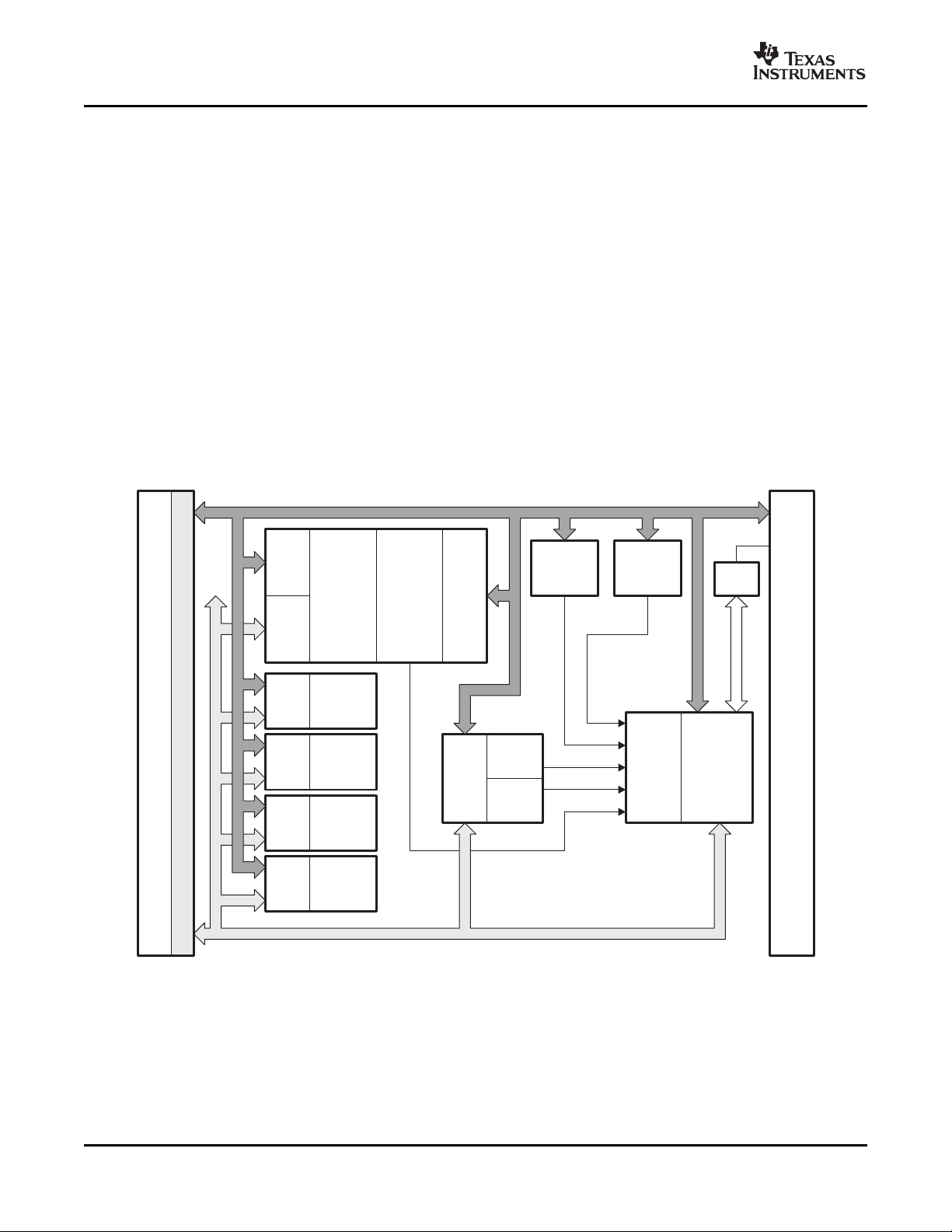
www.ti.com
ADVANCE INFORMATION
ADC
RESULT
registers
ADC
CPU
PF0
I/F
ADC
DMA
PF0
I/F
ADC
control
and
RESULT
registers
ADC
PF2
I/F
L4
I/F
L4
SARAM
(4Kx16)
L5
I/F
L5
SARAM
(4Kx16)
L6
I/F
L6
SARAM
(4Kx16)
L7
I/F
L7
SARAM
(4Kx16)
PF3
I/F
McBSP
A
McBSP
B
Event
triggers
DMA
6-ch
External
interrupts
CPU
timers
CPUbus
DMA bus
PIE
INT7
DINT[CH1:CH6]
CPU
XINTFzonesinterface
XINTFmemzones
TMS320F28335, TMS320F28334, TMS320F28332
TMS320F28235, TMS320F28234, TMS320F28232
Digital Signal Controllers (DSCs)
SPRS439C – JUNE 2007 – REVISED FEBRUARY 2008
4.1 DMA Overview
Features:
• 6 Channels with independent PIE interrupts
• Trigger Sources:
– ADC Sequencer 1 and Sequencer 2
– McBSP-A and McBSP-B transmit and receive logic
– XINT1-7 and XINT13
– CPU Timers
– Software
• Data Sources/Destinations:
– L4-L7 16k x 16 SARAM
– All XINTF zones
– ADC Memory Bus mapped RESULT registers
– McBSP-A and McBSP-B transmit and receive buffers
• Word Size: 16-bit or 32-bit (McBSPs limited to 16-bit)
• Throughput: 4 cycles/word (5 cycles/word for McBSP reads)
Peripherals 64 Submit Documentation Feedback
Figure 4-1. DMA Functional Block Diagram

www.ti.com
ADVANCE INFORMATION
4.2 32-Bit CPU-Timers 0/1/2
Borrow
Reset
Timer Reload
SYSCLKOUT
TCR.4
(Timer Start Status)
TINT
16-Bit Timer Divide-Down
TDDRH:TDDR
32-Bit Timer Period
PRDH:PRD
32-Bit Counter
TIMH:TIM
16-Bit Prescale Counter
PSCH:PSC
Borrow
INT1
to
INT12
INT14
28x
CPU
TINT2
TINT0
PIE
CPU-TIMER0
CPU-TIMER2
(ReservedforDSP/BIOS)
INT13
TINT1
CPU-TIMER1
XINT13
There are three 32-bit CPU-timers on the devices (CPU-TIMER0/1/2).
Timer 2 is reserved for DSP/BIOS™. CPU-Timer 0 and CPU-Timer 1 can be used in user applications.
These timers are different from the timers that are present in the ePWM modules.
NOTE: If the application is not using DSP/BIOS, then CPU-Timer 2 can be used in the
application.
TMS320F28335, TMS320F28334, TMS320F28332
TMS320F28235, TMS320F28234, TMS320F28232
Digital Signal Controllers (DSCs)
SPRS439C – JUNE 2007 – REVISED FEBRUARY 2008
NOTE
Figure 4-2. CPU-Timers
The timer interrupt signals ( TINT0, TINT1, TINT2) are connected as shown in Figure 4-3 .
A. The timer registers are connected to the memory bus of the C28x processor.
B. The timing of the timers is synchronized to SYSCLKOUT of the processor clock.
Figure 4-3. CPU-Timer Interrupt Signals and Output Signal
Submit Documentation Feedback Peripherals 65

www.ti.com
ADVANCE INFORMATION
TMS320F28335, TMS320F28334, TMS320F28332
TMS320F28235, TMS320F28234, TMS320F28232
Digital Signal Controllers (DSCs)
SPRS439C – JUNE 2007 – REVISED FEBRUARY 2008
The general operation of the timer is as follows: The 32-bit counter register "TIMH:TIM" is loaded with the
value in the period register "PRDH:PRD". The counter register decrements at the SYSCLKOUT rate of the
C28x. When the counter reaches 0, a timer interrupt output signal generates an interrupt pulse. The
registers listed in Table 4-1 are used to configure the timers. For more information, see the
TMS320F2833x Digital Signal Controller (DSC) System Control and Interrupts Reference Guide (literature
number SPRUFB0 )
Table 4-1. CPU-Timers 0, 1, 2 Configuration and Control Registers
NAME ADDRESS SIZE (x16) DESCRIPTION
TIMER0TIM 0x0C00 1 CPU-Timer 0, Counter Register
TIMER0TIMH 0x0C01 1 CPU-Timer 0, Counter Register High
TIMER0PRD 0x0C02 1 CPU-Timer 0, Period Register
TIMER0PRDH 0x0C03 1 CPU-Timer 0, Period Register High
TIMER0TCR 0x0C04 1 CPU-Timer 0, Control Register
Reserved 0x0C05 1
TIMER0TPR 0x0C06 1 CPU-Timer 0, Prescale Register
TIMER0TPRH 0x0C07 1 CPU-Timer 0, Prescale Register High
TIMER1TIM 0x0C08 1 CPU-Timer 1, Counter Register
TIMER1TIMH 0x0C09 1 CPU-Timer 1, Counter Register High
TIMER1PRD 0x0C0A 1 CPU-Timer 1, Period Register
TIMER1PRDH 0x0C0B 1 CPU-Timer 1, Period Register High
TIMER1TCR 0x0C0C 1 CPU-Timer 1, Control Register
Reserved 0x0C0D 1
TIMER1TPR 0x0C0E 1 CPU-Timer 1, Prescale Register
TIMER1TPRH 0x0C0F 1 CPU-Timer 1, Prescale Register High
TIMER2TIM 0x0C10 1 CPU-Timer 2, Counter Register
TIMER2TIMH 0x0C11 1 CPU-Timer 2, Counter Register High
TIMER2PRD 0x0C12 1 CPU-Timer 2, Period Register
TIMER2PRDH 0x0C13 1 CPU-Timer 2, Period Register High
TIMER2TCR 0x0C14 1 CPU-Timer 2, Control Register
Reserved 0x0C15 1
TIMER2TPR 0x0C16 1 CPU-Timer 2, Prescale Register
TIMER2TPRH 0x0C17 1 CPU-Timer 2, Prescale Register High
Reserved 40
0x0C18
0x0C3F
Peripherals 66 Submit Documentation Feedback
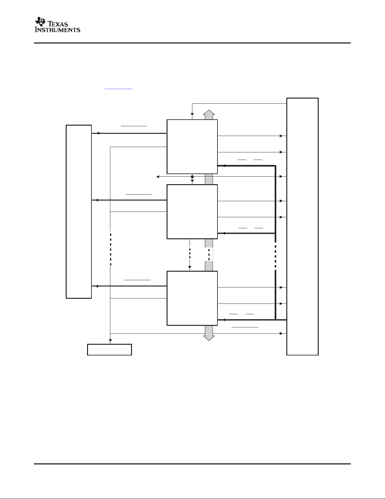
www.ti.com
ADVANCE INFORMATION
4.3 Enhanced PWM Modules (ePWM1/2/3/4/5/6)
PIE
TZ1
to TZ6
Peripheral Bus
ePWM1 module
ePWM2 module
ePWMx module
EPWM1SYNCI
EPWM2SYNCI
EPWM2SYNCO
EPWMxSYNCI
EPWMxSYNCO
ADC
GPIO
MUX
EPWM1SYNCI
EPWM1SYNCO
ADCSOCx0
EPWMxA
EPWMxB
EPWM2A
EPWM2B
EPWM1A
EPWM1B
EPWM1INT
EPWM1SOC
EPWM2INT
EPWM2SOC
EPWMxINT
EPWMxSOC
to eCAP1
module
(sync in)
TZ1 to TZ6
TZ1 to TZ6
.
EPWM1SYNCO
The F2833x/F2823x devices contain up to six enhanced PWM Modules (ePWM). Figure 4-4 shows a
block diagram of multiple ePWM modules. Figure 4-4 shows the signal interconnections with the ePWM.
See the TMS320x28xx, 28xxx Enhanced Pulse Width Modulator (ePWM) Module Reference Guide
(literature number SPRU791 ) for more details.
TMS320F28335, TMS320F28334, TMS320F28332
TMS320F28235, TMS320F28234, TMS320F28232
Digital Signal Controllers (DSCs)
SPRS439C – JUNE 2007 – REVISED FEBRUARY 2008
Figure 4-4. Multiple PWM Modules in a F2833x/F2823x System
Table 4-2 shows the complete ePWM register set per module.
Submit Documentation Feedback Peripherals 67

www.ti.com
TMS320F28335, TMS320F28334, TMS320F28332
TMS320F28235, TMS320F28234, TMS320F28232
Digital Signal Controllers (DSCs)
SPRS439C – JUNE 2007 – REVISED FEBRUARY 2008
Table 4-2. ePWM Control and Status Registers
NAME EPWM1 EPWM2 EPWM3 EPWM4 EPWM5 EPWM6 DESCRIPTION
TBCTL 0x6800 0x6840 0x6880 0x68C0 0x6900 0x6940 1 / 0 Time Base Control Register
TBSTS 0x6801 0x6841 0x6881 0x68C1 0x6901 0x6941 1 / 0 Time Base Status Register
TBPHSHR 0x6802 0x6842 0x6882 0x68C2 0x6902 0x6942 1 / 0 Time Base Phase HRPWM Register
TBPHS 0x6803 0x6843 0x6883 0x68C3 0x6903 0x6943 1 / 0 Time Base Phase Register
TBCTR 0x6804 0x6844 0x6884 0x68C4 0x6904 0x6944 1 / 0 Time Base Counter Register
TBPRD 0x6805 0x6845 0x6885 0x68C5 0x6905 0x6945 1 / 1 Time Base Period Register Set
CMPCTL 0x6807 0x6847 0x6887 0x68C7 0x6907 0x6947 1 / 0 Counter Compare Control Register
CMPAHR 0x6808 0x6848 0x6888 0x68C8 0x6908 0x6948 1 / 1 Time Base Compare A HRPWM Register
CMPA 0x6809 0x6849 0x6889 0x68C9 0x6909 0x6949 1 / 1 Counter Compare A Register Set
CMPB 0x680A 0x684A 0x688A 0x68CA 0x690A 0x694A 1 / 1 Counter Compare B Register Set
AQCTLA 0x680B 0x684B 0x688B 0x68CB 0x690B 0x694B 1 / 0 Action Qualifier Control Register For Output A
AQCTLB 0x680C 0x684C 0x688C 0x68CC 0x690C 0x694C 1 / 0 Action Qualifier Control Register For Output B
AQSFRC 0x680D 0x684D 0x688D 0x68CD 0x690D 0x694D 1 / 0 Action Qualifier Software Force Register
AQCSFRC 0x680E 0x684E 0x688E 0x68CE 0x690E 0x694E 1 / 1 Action Qualifier Continuous S/W Force Register Set
DBCTL 0x680F 0x684F 0x688F 0x68CF 0x690F 0x694F 1 / 1 Dead-Band Generator Control Register
DBRED 0x6810 0x6850 0x6890 0x68D0 0x6910 0x6950 1 / 0 Dead-Band Generator Rising Edge Delay Count Register
DBFED 0x6811 0x6851 0x6891 0x68D1 0x6911 0x6951 1 / 0 Dead-Band Generator Falling Edge Delay Count Register
TZSEL 0x6812 0x6852 0x6892 0x68D2 0x6912 0x6952 1 / 0 Trip Zone Select Register
TZCTL 0x6814 0x6854 0x6894 0x68D4 0x6914 0x6954 1 / 0 Trip Zone Control Register
TZEINT 0x6815 0x6855 0x6895 0x68D5 0x6915 0x6955 1 / 0 Trip Zone Enable Interrupt Register
TZFLG 0x6816 0x6856 0x6896 0x68D6 0x6916 0x6956 1 / 0 Trip Zone Flag Register
TZCLR 0x6817 0x6857 0x6897 0x68D7 0x6917 0x6957 1 / 0 Trip Zone Clear Register
TZFRC 0x6818 0x6858 0x6898 0x68D8 0x6918 0x6958 1 / 0 Trip Zone Force Register
ETSEL 0x6819 0x6859 0x6899 0x68D9 0x6919 0x6959 1 / 0 Event Trigger Selection Register
ETPS 0x681A 0x685A 0x689A 0x68DA 0x691A 0x695A 1 / 0 Event Trigger Prescale Register
ETFLG 0x681B 0x685B 0x689B 0x68DB 0x691B 0x695B 1 / 0 Event Trigger Flag Register
ETCLR 0x681C 0x685C 0x689C 0x68DC 0x691C 0x695C 1 / 0 Event Trigger Clear Register
ETFRC 0x681D 0x685D 0x689D 0x68DD 0x691D 0x695D 1 / 0 Event Trigger Force Register
PCCTL 0x681E 0x685E 0x689E 0x68DE 0x691E 0x695E 1 / 0 PWM Chopper Control Register
HRCNFG 0x6820 0x6860 0x68A0 0x68E0 0x6920 0x6960 1 / 0 HRPWM Configuration Register
SIZE (x16) /
#SHADOW
(1)
(1)
(1)
(1)
(1)
(1)
(1) Registers that are EALLOW protected.
68 Peripherals Submit Documentation Feedback

www.ti.com
ADVANCE INFORMATION
CTR=PRD
TBPRD shadow (16)
TBPRD active (16)
Counter
up/down
(16 bit)
TBCNT
active (16)
TBCTL[CNTLDE]
TBCTL[SWFSYNC]
(software forced sync)
EPWMxSYNCI
CTR=ZERO
CTR_Dir
CTR=CMPB
Disabled
Sync
in/out
select
Mux
TBCTL[SYNCOSEL]
EPWMxSYNCO
TBPHS active (24)
16
8
TBPHSHR (8)
Phase
control
Time−base (TB)
CTR=CMPA
CMPA active (24)
16
CMPA shadow (24)
Action
qualifier
(AQ)
8
16
Counter compare (CC)
CMPB active (16)
CTR=CMPB
CMPB shadow (16)
CMPAHR (8)
EPWMA
EPWMB
Dead
band
(DB) (PC)
chopper
PWM
zone
(TZ)
Trip
CTR = ZERO
EPWMxAO
EPWMxBO
EPWMxTZINT
TZ1 to TZ6
HiRes PWM (HRPWM)
CTR = PRD
CTR = ZERO
CTR = CMPB
CTR = CMPA
CTR_Dir
Event
trigger
and
interrupt
(ET)
EPWMxINT
EPWMxSOCA
EPWMxSOCB
CTR=ZERO
TMS320F28335, TMS320F28334, TMS320F28332
TMS320F28235, TMS320F28234, TMS320F28232
Digital Signal Controllers (DSCs)
SPRS439C – JUNE 2007 – REVISED FEBRUARY 2008
4.4 High-Resolution PWM (HRPWM)
Figure 4-5. ePWM Sub-Modules Showing Critical Internal Signal Interconnections
The HRPWM module offers PWM resolution (time granularity) which is significantly better than what can
be achieved using conventionally derived digital PWM methods. The key points for the HRPWM module
are:
• Significantly extends the time resolution capabilities of conventionally derived digital PWM
• Typically used when effective PWM resolution falls below ~ 9-10 bits. This occurs at PWM frequencies
greater than ~200 KHz when using a CPU/System clock of 100 MHz.
• This capability can be utilized in both duty cycle and phase-shift control methods.
• Finer time granularity control or edge positioning is controlled via extensions to the Compare A and
Phase registers of the ePWM module.
• HRPWM capabilities are offered only on the A signal path of an ePWM module (i.e., on the EPWMxA
output). EPWMxB output has conventional PWM capabilities.
Submit Documentation Feedback Peripherals 69
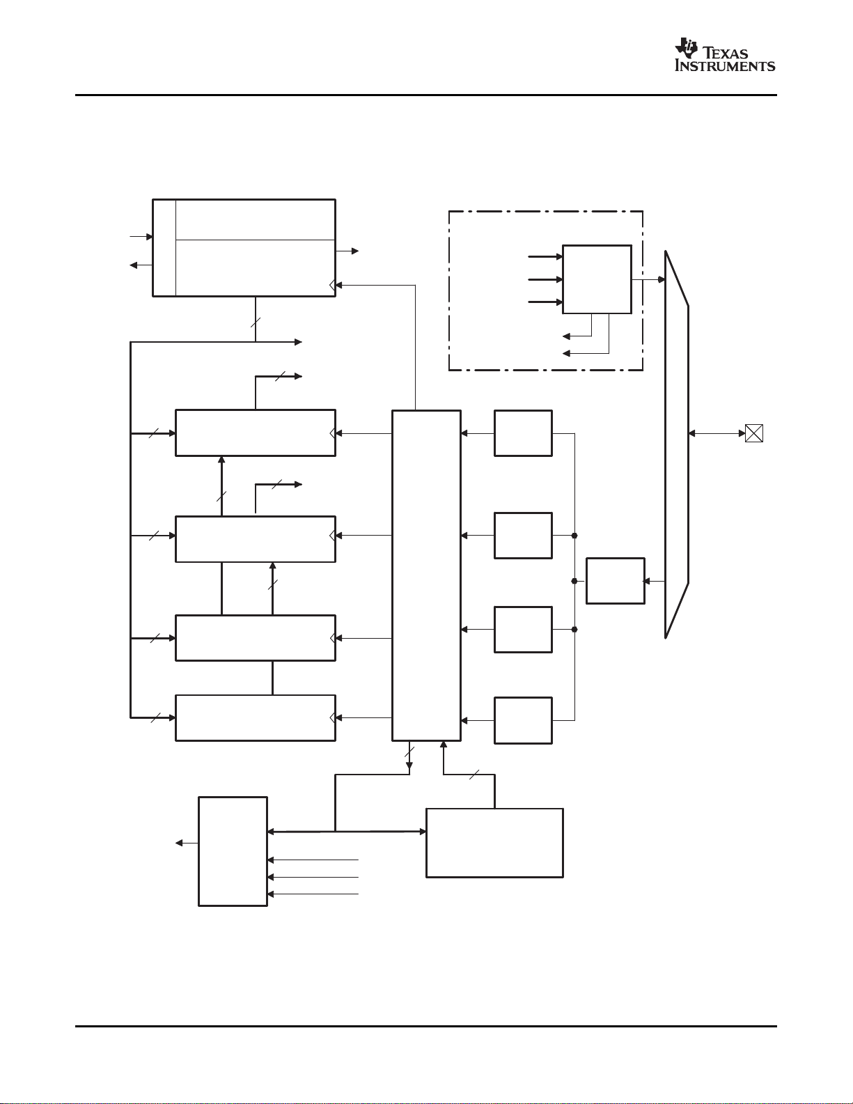
www.ti.com
ADVANCE INFORMATION
TSCTR
(counter−32 bit)
RST
CAP1
(APRD active)
LD
CAP2
(ACMP active)
LD
CAP3
(APRD shadow)
LD
CAP4
(ACMP shadow)
LD
Continuous /
Oneshot
Capture Control
LD1
LD2
LD3
LD4
32
32
PRD [0−31]
CMP [0−31]
CTR [0−31]
eCAPx
Interrupt
Trigger
and
Flag
control
to PIE
CTR=CMP
32
32
32
32
32
ACMP
shadow
Event
Pre-scale
CTRPHS
(phase register−32 bit)
SYNCOut
SYNCIn
Event
qualifier
Polarity
select
Polarity
select
Polarity
select
Polarity
select
CTR=PRD
CTR_OVF
4
PWM
compare
logic
CTR [0−31]
PRD [0−31]
CMP [0−31]
CTR=CMP
CTR=PRD
CTR_OVF
OVF
APWM mode
Delta−mode
SYNC
4
Capture events
CEVT[1:4]
APRD
shadow
32
32
MODE SELECT
TMS320F28335, TMS320F28334, TMS320F28332
TMS320F28235, TMS320F28234, TMS320F28232
Digital Signal Controllers (DSCs)
SPRS439C – JUNE 2007 – REVISED FEBRUARY 2008
4.5 Enhanced CAP Modules (eCAP1/2/3/4/5/6)
The F2833x/F2823x device contains up to six enhanced capture (eCAP) modules. Figure 4-6 shows a
functional block diagram of a module. See the TMS320x28xx, 28xxx Enhanced Capture (eCAP) Module
Reference Guide (literature number SPRU807) for more details.
The eCAP modules are clocked at the SYSCLKOUT rate.
Peripherals 70 Submit Documentation Feedback
Figure 4-6. eCAP Functional Block Diagram

www.ti.com
ADVANCE INFORMATION
TMS320F28335, TMS320F28334, TMS320F28332
TMS320F28235, TMS320F28234, TMS320F28232
Digital Signal Controllers (DSCs)
SPRS439C – JUNE 2007 – REVISED FEBRUARY 2008
The clock enable bits (ECAP1/2/3/4/5/6ENCLK) in the PCLKCR1 register are used to turn off the eCAP
modules individually (for low power operation). Upon reset, ECAP1ENCLK, ECAP2ENCLK,
ECAP3ENCLK, ECAP4ENCLK, ECAP5ENCLK, and ECAP6ENCLK are set to low, indicating that the
peripheral clock is off.
Table 4-3. eCAP Control and Status Registers
NAME ECAP1 ECAP2 ECAP3 ECAP4 ECAP5 ECAP6 DESCRIPTION
TSCTR 0x6A00 0x6A20 0x6A40 0x6A60 0x6A80 0x6AA0 2 Time-Stamp Counter
CTRPHS 0x6A02 0x6A22 0x6A42 0x6A62 0x6A82 0x6AA2 2 Counter Phase Offset Value
CAP1 0x6A04 0x6A24 0x6A44 0x6A64 0x6A84 0x6AA4 2 Capture 1 Register
CAP2 0x6A06 0x6A26 0x6A46 0x6A66 0x6A86 0x6AA6 2 Capture 2 Register
CAP3 0x6A08 0x6A28 0x6A48 0x6A68 0x6A88 0x6AA8 2 Capture 3 Register
CAP4 0x6A0A 0x6A2A 0x6A4A 0x6A6A 0x6A8A 0x6AAA 2 Capture 4 Register
Reserved 0x6A0C- 0x6A2C- 0x6A4C- 0x6A6C- 0x6A8C- 0x6AAC- 8 Reserved
0x6A12 0x6A32 0x6A52 0x6A72 0x6A92 0x6AB2
ECCTL1 0x6A14 0x6A34 0x6A54 0x6A74 0x6A94 0x6AB4 1 Capture Control Register 1
ECCTL2 0x6A15 0x6A35 0x6A55 0x6A75 0x6A95 0x6AB5 1 Capture Control Register 2
ECEINT 0x6A16 0x6A36 0x6A56 0x6A76 0x6A96 0x6AB6 1 Capture Interrupt Enable Register
ECFLG 0x6A17 0x6A37 0x6A57 0x6A77 0x6A97 0x6AB7 1 Capture Interrupt Flag Register
ECCLR 0x6A18 0x6A38 0x6A58 0x6A78 0x6A98 0x6AB8 1 Capture Interrupt Clear Register
ECFRC 0x6A19 0x6A39 0x6A59 0x6A79 0x6A99 0x6AB9 1 Capture Interrupt Force Register
Reserved 0x6A1A- 0x6A3A- 0x6A5A- 0x6A7A- 0x6A9A- 0x6ABA- 6 Reserved
0x6A1F 0x6A3F 0x6A5F 0x6A7F 0x6A9F 0x6ABF
SIZE
(x16)
Register
Submit Documentation Feedback Peripherals 71

www.ti.com
ADVANCE INFORMATION
QWDTMR
QWDPRD
16
QWDOGUTIME
QUPRD
QUTMR
32
UTOUT
WDTOUT
Quadrature
capture unit
(QCAP)
QCPRDLAT
QCTMRLAT
16
QFLG
QEPSTS
QEPCTL
Registers
used by
multiple units
QCLK
QDIR
QI
QS
PHE
PCSOUT
Quadrature
decoder
(QDU)
QDECCTL
16
Position counter/
control unit
(PCCU)
QPOSLAT
QPOSSLAT
16
QPOSILAT
EQEPxAIN
EQEPxBIN
EQEPxIIN
EQEPxIOUT
EQEPxIOE
EQEPxSIN
EQEPxSOUT
EQEPxSOE
GPIO
MUX
EQEPxA/XCLK
EQEPxB/XDIR
EQEPxS
EQEPxI
QPOSCMP
QEINT
QFRC
32
QCLR
QPOSCTL
1632
QPOSCNT
QPOSMAX
QPOSINIT
PIE
EQEPxINT
Enhanced QEP (eQEP) peripheral
System
control registers
QCTMR
QCPRD
1616
QCAPCTL
EQEPxENCLK
SYSCLKOUT
Data bus
To CPU
TMS320F28335, TMS320F28334, TMS320F28332
TMS320F28235, TMS320F28234, TMS320F28232
Digital Signal Controllers (DSCs)
SPRS439C – JUNE 2007 – REVISED FEBRUARY 2008
4.6 Enhanced QEP Modules (eQEP1/2)
The device contains up to two enhanced quadrature encoder (eQEP) modules. See the TMS320x28xx,
28xxx Enhanced Quadrature Encoder (eQEP) Module Reference Guide (literature number SPRU790) for
more details.
Figure 4-7. eQEP Functional Block Diagram
72 Peripherals Submit Documentation Feedback

www.ti.com
ADVANCE INFORMATION
TMS320F28335, TMS320F28334, TMS320F28332
TMS320F28235, TMS320F28234, TMS320F28232
Digital Signal Controllers (DSCs)
SPRS439C – JUNE 2007 – REVISED FEBRUARY 2008
Table 4-4. eQEP Control and Status Registers
NAME SIZE(x16)/ REGISTER DESCRIPTION
QPOSCNT 0x6B00 0x6B40 2/0 eQEP Position Counter
QPOSINIT 0x6B02 0x6B42 2/0 eQEP Initialization Position Count
QPOSMAX 0x6B04 0x6B44 2/0 eQEP Maximum Position Count
QPOSCMP 0x6B06 0x6B46 2/1 eQEP Position-compare
QPOSILAT 0x6B08 0x6B48 2/0 eQEP Index Position Latch
QPOSSLAT 0x6B0A 0x6B4A 2/0 eQEP Strobe Position Latch
QPOSLAT 0x6B0C 0x6B4C 2/0 eQEP Position Latch
QUTMR 0x6B0E 0x6B4E 2/0 eQEP Unit Timer
QUPRD 0x6B10 0x6B50 2/0 eQEP Unit Period Register
QWDTMR 0x6B12 0x6B52 1/0 eQEP Watchdog Timer
QWDPRD 0x6B13 0x6B53 1/0 eQEP Watchdog Period Register
QDECCTL 0x6B14 0x6B54 1/0 eQEP Decoder Control Register
QEPCTL 0x6B15 0x6B55 1/0 eQEP Control Register
QCAPCTL 0x6B16 0x6B56 1/0 eQEP Capture Control Register
QPOSCTL 0x6B17 0x6B57 1/0 eQEP Position-compare Control Register
QEINT 0x6B18 0x6B58 1/0 eQEP Interrupt Enable Register
QFLG 0x6B19 0x6B59 1/0 eQEP Interrupt Flag Register
QCLR 0x6B1A 0x6B5A 1/0 eQEP Interrupt Clear Register
QFRC 0x6B1B 0x6B5B 1/0 eQEP Interrupt Force Register
QEPSTS 0x6B1C 0x6B5C 1/0 eQEP Status Register
QCTMR 0x6B1D 0x6B5D 1/0 eQEP Capture Timer
QCPRD 0x6B1E 0x6B5E 1/0 eQEP Capture Period Register
QCTMRLAT 0x6B1F 0x6B5F 1/0 eQEP Capture Timer Latch
QCPRDLAT 0x6B20 0x6B60 1/0 eQEP Capture Period Latch
Reserved 0x6B21- 0x6B61- 31/0
EQEP1 EQEP2
ADDRESS ADDRESS
0x6B3F 0x6B7F
EQEP1
#SHADOW
Submit Documentation Feedback Peripherals 73

www.ti.com
ADVANCE INFORMATION
Digital Value + 0,
Digital Value + 4096
Input Analog Voltage* ADCLO
3
when input ≤ 0 V
when 0 V < input < 3 V
when input ≥ 3 VDigital V alue + 4095,
TMS320F28335, TMS320F28334, TMS320F28332
TMS320F28235, TMS320F28234, TMS320F28232
Digital Signal Controllers (DSCs)
SPRS439C – JUNE 2007 – REVISED FEBRUARY 2008
4.7 Analog-to-Digital Converter (ADC) Module
A simplified functional block diagram of the ADC module is shown in Figure 4-8 . The ADC module
consists of a 12-bit ADC with a built-in sample-and-hold (S/H) circuit. Functions of the ADC module
include:
• 12-bit ADC core with built-in S/H
• Analog input: 0.0 V to 3.0 V (Voltages above 3.0 V produce full-scale conversion results.)
• Fast conversion rate: Up to 80 ns at 25-MHz ADC clock, 12.5 MSPS
• 16-channel, MUXed inputs
• Autosequencing capability provides up to 16 "autoconversions" in a single session. Each conversion
can be programmed to select any 1 of 16 input channels
• Sequencer can be operated as two independent 8-state sequencers or as one large 16-state
sequencer (i.e., two cascaded 8-state sequencers)
• Sixteen result registers (individually addressable) to store conversion values
– The digital value of the input analog voltage is derived by:
A. All fractional values are truncated.
• Multiple triggers as sources for the start-of-conversion (SOC) sequence
– S/W - software immediate start
– ePWM start of conversion
– XINT2 ADC start of conversion
• Flexible interrupt control allows interrupt request on every end-of-sequence (EOS) or every other EOS.
• Sequencer can operate in "start/stop" mode, allowing multiple "time-sequenced triggers" to
synchronize conversions.
• SOCA and SOCB triggers can operate independently in dual-sequencer mode.
• Sample-and-hold (S/H) acquisition time window has separate prescale control.
The ADC module in the F2833x/F2823x devices has been enhanced to provide flexible interface to ePWM
peripherals. The ADC interface is built around a fast, 12-bit ADC module with a fast conversion rate of up
to 80 ns at 25-MHz ADC clock. The ADC module has 16 channels, configurable as two independent
8-channel modules. The two independent 8-channel modules can be cascaded to form a 16-channel
module. Although there are multiple input channels and two sequencers, there is only one converter in the
ADC module. Figure 4-8 shows the block diagram of the ADC module.
The two 8-channel modules have the capability to autosequence a series of conversions, each module
has the choice of selecting any one of the respective eight channels available through an analog MUX. In
the cascaded mode, the autosequencer functions as a single 16-channel sequencer. On each sequencer,
once the conversion is complete, the selected channel value is stored in its respective RESULT register.
Autosequencing allows the system to convert the same channel multiple times, allowing the user to
perform oversampling algorithms. This gives increased resolution over traditional single-sampled
conversion results.
Peripherals 74 Submit Documentation Feedback
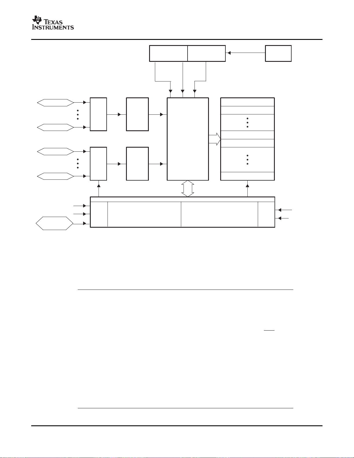
www.ti.com
ADVANCE INFORMATION
ResultRegisters
EPWMSOCB
S/W
GPIO/
XINT2_ADCSOC
EPWMSOCA
S/W
Sequencer2
Sequencer1
SOCSOC
ADCControlRegisters
70B7h
70B0h
70AFh
70A8h
ResultReg15
ResultReg8
ResultReg7
ResultReg1
ResultReg0
12-Bit
ADC
Module
Analog
MUX
ADCINA0
ADCINA7
ADCINB0
ADCINB7
System
ControlBlock
High-Speed
Prescaler
HSPCLK
ADCENCLK
DSP
SYSCLKOUT
S/H
S/H
HALT
TMS320F28335, TMS320F28334, TMS320F28332
TMS320F28235, TMS320F28234, TMS320F28232
Digital Signal Controllers (DSCs)
SPRS439C – JUNE 2007 – REVISED FEBRUARY 2008
Figure 4-8. Block Diagram of the ADC Module
To obtain the specified accuracy of the ADC, proper board layout is very critical. To the best extent
possible, traces leading to the ADCIN pins should not run in close proximity to the digital signal paths.
This is to minimize switching noise on the digital lines from getting coupled to the ADC inputs.
Furthermore, proper isolation techniques must be used to isolate the ADC module power pins ( V
V
DD2A18
, V
, V
DDA2
1. The ADC registers are accessed at the SYSCLKOUT rate. The internal timing of the
) from the digital supply.Figure 4-9 shows the ADC pin connections for the devices.
DDAIO
ADC module is controlled by the high-speed peripheral clock (HSPCLK).
2. The behavior of the ADC module based on the state of the ADCENCLK and HALT
NOTE
signals is as follows:
– ADCENCLK: On reset, this signal will be low. While reset is active-low ( XRS) the
clock to the register will still function. This is necessary to make sure all registers
and modes go into their default reset state. The analog module, however, will be
in a low-power inactive state. As soon as reset goes high, then the clock to the
registers will be disabled. When the user sets the ADCENCLK signal high, then
the clocks to the registers will be enabled and the analog module will be enabled.
There will be a certain time delay (ms range) before the ADC is stable and can be
used.
– HALT: This mode only affects the analog module. It does not affect the registers.
In this mode, the ADC module goes into low-power mode. This mode also will stop
the clock to the CPU, which will stop the HSPCLK; therefore, the ADC register
logic will be turned off indirectly.
,
DD1A18
Submit Documentation Feedback Peripherals 75

www.ti.com
ADVANCE INFORMATION
ADCINA[7:0]
ADCINB[7:0]
ADCLO
ADCREFIN
ADCExternalCurrentBiasResistor ADCRESEXT
ADCREFP
V
DD1A18
V
DD2A18
V
SS1AGND
V
SS2AGND
V
DDAIO
V
SSAIO
V
DDA2
V
SSA2
ADCReferencePositiveOutput
ADCREFMADCReferenceMediumOutput
ADCPower
ADCAnalogandReferenceI/OPower
Analoginput0−3VwithrespecttoADCLO
Connecttoanalogground
22kΩ
2.2 μF
(A)
ADCAnalogPowerPin(1.9V)
ADCAnalogPowerPin(1.9V)
ADCAnalogPowerPin(3.3V)
ADCAnalogI/OGroundPin
ADCAnalogPowerPin(3.3V)
ADCREFPandADCREFMshouldnot
beloadedbyexternalcircuitry
ADCAnalogGroundPin
ADC16-ChannelAnalogInputs
Floatorgroundifinternalreferenceisused
ADCAnalogGroundPin
ADCAnalogGroundPin
2.2 μF
(A)
ADCINA[7:0]
ADCINB[7:0]
ADCLO
ADCREFIN
ADCExternalCurrentBiasResistor ADCRESEXT
ADCREFP
V
DD1A18
V
DD2A18
V
SS1AGND
V
SS2AGND
V
DDAIO
V
SSAIO
V
DDA2
V
SSA2
ADCReferencePositiveOutput
ADCREFMADCReferenceMediumOutput
ADC AnalogPower
ADC AnalogandReferenceI/OPower
Analoginput0−3Vwithrespectto ADCLO
Connectto AnalogGround
22kΩ
2.2 µF
(A)
ADCREFP and ADCREFMshouldnot
beloadedbyexternalcircuitry
ADC16-Channel AnalogInputs
Connectto1.500,1.024,or2.048-Vprecisionsource
(D)
ADC AnalogPowerPin(1.9V)
ADC AnalogPowerPin(1.9V)
ADC AnalogI/OGroundPin
ADC AnalogPowerPin(3.3V)
ADC AnalogGroundPin
ADC AnalogGroundPin
ADC AnalogGroundPin
ADC AnalogPowerPin(3.3V)
2.2 µF
(A)
TMS320F28335, TMS320F28334, TMS320F28332
TMS320F28235, TMS320F28234, TMS320F28232
Digital Signal Controllers (DSCs)
SPRS439C – JUNE 2007 – REVISED FEBRUARY 2008
Figure 4-9 shows the ADC pin-biasing for internal reference and Figure 4-10 shows the ADC pin-biasing
for external reference.
A. TAIYO YUDEN LMK212BJ225MG-T or equivalent
B. External decoupling capacitors are recommended on all power pins.
C. Analog inputs must be driven from an operational amplifier that does not degrade the ADC performance.
A. TAIYO YUDEN LMK212BJ225MG-T or equivalent
B. External decoupling capacitors are recommended on all power pins.
C. Analog inputs must be driven from an operational amplifier that does not degrade the ADC performance.
D. External voltage on ADCREFIN is enabled by changing bits 15:14 in the ADC Reference Select register depending on
the voltage used on this pin. TI recommends TI part REF3020 or equivalent for 2.048-V generation. Overall gain
accuracy will be determined by accuracy of this voltage source.
Peripherals 76 Submit Documentation Feedback
Figure 4-9. ADC Pin Connections With Internal Reference
Figure 4-10. ADC Pin Connections With External Reference

www.ti.com
ADVANCE INFORMATION
The temperature rating of any recommended component must match the rating of the end
product.
4.7.1 ADC Connections if the ADC Is Not Used
It is recommended to keep the connections for the analog power pins, even if the ADC is not used.
Following is a summary of how the ADC pins should be connected, if the ADC is not used in an
application:
• V
• V
• V
• ADCLO – Connect to V
• ADCREFIN – Connect to V
• ADCREFP/ADCREFM – Connect a 100-nF cap to V
• ADCRESEXT – Connect a 20-k Ω resistor (very loose tolerance) to V
• ADCINAn, ADCINBn - Connect to V
When the ADC is not used, be sure that the clock to the ADC module is not turned on to realize power
savings.
/V
DD1A18
DDA2
SS1AGND
DD2A18
, V
DDAIO
/V
– Connect to V
– Connect to V
SS2AGND
DD
DDIO
, V
, V
SSA2
SSAIO
SS
SS
– Connect to V
SS
TMS320F28335, TMS320F28334, TMS320F28332
TMS320F28235, TMS320F28234, TMS320F28232
NOTE
SS
SS
Digital Signal Controllers (DSCs)
SPRS439C – JUNE 2007 – REVISED FEBRUARY 2008
.
SS
When the ADC module is used in an application, unused ADC input pins should be connected to analog
ground (V
SS1AGND
/V
SS2AGND
)
NOTE
ADC parameters for gain error and offset error are specified only if the ADC calibration
routine is executed from the Boot ROM. See Section 4.7.3 for more information.
4.7.2 ADC Registers
The ADC operation is configured, controlled, and monitored by the registers listed in Table 4-5 .
Table 4-5. ADC Registers
NAME ADDRESS
ADCTRL1 0x7100 1 ADC Control Register 1
ADCTRL2 0x7101 1 ADC Control Register 2
ADCMAXCONV 0x7102 1 ADC Maximum Conversion Channels Register
ADCCHSELSEQ1 0x7103 1 ADC Channel Select Sequencing Control Register 1
ADCCHSELSEQ2 0x7104 1 ADC Channel Select Sequencing Control Register 2
ADCCHSELSEQ3 0x7105 1 ADC Channel Select Sequencing Control Register 3
ADCCHSELSEQ4 0x7106 1 ADC Channel Select Sequencing Control Register 4
ADCASEQSR 0x7107 1 ADC Auto-Sequence Status Register
ADCRESULT0 0x7108 0x0B00 1 ADC Conversion Result Buffer Register 0
ADCRESULT1 0x7109 0x0B01 1 ADC Conversion Result Buffer Register 1
ADCRESULT2 0x710A 0x0B02 1 ADC Conversion Result Buffer Register 2
ADCRESULT3 0x710B 0x0B03 1 ADC Conversion Result Buffer Register 3
ADCRESULT4 0x710C 0x0B04 1 ADC Conversion Result Buffer Register 4
ADCRESULT5 0x710D 0x0B05 1 ADC Conversion Result Buffer Register 5
(1)
ADDRESS
(2)
SIZE (x16) DESCRIPTION
(1)
(1) The registers in this column are Peripheral Frame 2 Registers.
(2) The ADC result registers are dual mapped. Locations in Peripheral Frame 2 (0x7108-0x7117) are 2 wait-states and left justified.
Locations in Peripheral frame 0 space (0x0B00-0x0B0F) are 1 wait-state for CPU accesses and 0 wait state for DMA accesses and right
justified. During high speed/continuous conversion use of the ADC, use the 0 wait-state locations for fast transfer of ADC results to user
memory.
Submit Documentation Feedback Peripherals 77
www.ti.com
ADVANCE INFORMATION
TMS320F28335, TMS320F28334, TMS320F28332
TMS320F28235, TMS320F28234, TMS320F28232
Digital Signal Controllers (DSCs)
SPRS439C – JUNE 2007 – REVISED FEBRUARY 2008
Table 4-5. ADC Registers (continued)
NAME ADDRESS
ADCRESULT6 0x710E 0x0B06 1 ADC Conversion Result Buffer Register 6
ADCRESULT7 0x710F 0x0B07 1 ADC Conversion Result Buffer Register 7
ADCRESULT8 0x7110 0x0B08 1 ADC Conversion Result Buffer Register 8
ADCRESULT9 0x7111 0x0B09 1 ADC Conversion Result Buffer Register 9
ADCRESULT10 0x7112 0x0B0A 1 ADC Conversion Result Buffer Register 10
ADCRESULT11 0x7113 0x0B0B 1 ADC Conversion Result Buffer Register 11
ADCRESULT12 0x7114 0x0B0C 1 ADC Conversion Result Buffer Register 12
ADCRESULT13 0x7115 0x0B0D 1 ADC Conversion Result Buffer Register 13
ADCRESULT14 0x7116 0x0B0E 1 ADC Conversion Result Buffer Register 14
ADCRESULT15 0x7117 0x0B0F 1 ADC Conversion Result Buffer Register 15
ADCTRL3 0x7118 1 ADC Control Register 3
ADCST 0x7119 1 ADC Status Register
Reserved 2
ADCREFSEL 0x711C 1 ADC Reference Select Register
ADCOFFTRIM 0x711D 1 ADC Offset Trim Register
Reserved 2
(1)
ADDRESS
0x711A
0x711B
0x711E
0x711F
(2)
SIZE (x16) DESCRIPTION
4.7.3 ADC Calibration
The ADC_cal() routine is programmed into TI reserved OTP memory by the factory. The boot ROM
automatically calls the ADC_cal() routine to initialize the ADCREFSEL and ADCOFFTRIM registers with
device specific calibration data. During normal operation, this process occurs automatically and no action
is required by the user.
If the boot ROM is bypassed by Code Composer Studio during the development process, then
ADCREFSEL and ADCOFFTRIM must be initialized by the application. For working examples, see the
ADC initialization in the C2833x C/C++ Header Files and Peripheral Examples (SPRC530 ). Methods for
calling the ADC_cal() routine from an application are described in TMS3202833x Analog-to-Digital
Converter (ADC) Module Reference Guide (SPRU812 ).
NOTE
FAILURE TO INITIALIZE THESE REGISTERS WILL CAUSE THE ADC TO FUNCTION
OUT OF SPECIFICATION.
Because TI reserved OTP memory is secure, the ADC_Cal() routine must be called from
secure memory or called from non-secure memory after the Code Security Module is
unlocked. If the system is reset or the ADC module is reset using Bit 14 (RESET) from the
ADC Control Register 1, the routine must be repeated.
Peripherals 78 Submit Documentation Feedback

www.ti.com
ADVANCE INFORMATION
4.8 Multichannel Buffered Serial Port (McBSP) Module
( )
CLKSRG
CLKG =
1 + CLKGDV
The McBSP module has the following features:
• Compatible to McBSP in TMS320C54x™/ TMS320C55x™ DSC devices
• Full–duplex communication
• Double–buffered data registers that allow a continuous data stream
• Independent framing and clocking for receive and transmit
• External shift clock generation or an internal programmable frequency shift clock
• A wide selection of data sizes including 8–, 12–, 16–, 20–, 24–, or 32–bits
• 8–bit data transfers with LSB or MSB first
• Programmable polarity for both frame synchronization and data clocks
• Highly programmable internal clock and frame generation
• Direct interface to industry–standard CODECs, Analog Interface Chips (AICs), and other serially
connected A/D and D/A devices
• Works with SPI–compatible devices
The following application interfaces can be supported on the McBSP:
• T1/E1 framers
• MVIP switching–compatible and ST–BUS–compliant devices including:
– MVIP framers
– H.100 framers
– SCSA framers
– IOM–2 compliant devices
– AC97–compliant devices (the necessary multiphase frame synchronization capability is provided.)
– IIS–compliant devices
• McBSP clock rate,
TMS320F28335, TMS320F28334, TMS320F28332
TMS320F28235, TMS320F28234, TMS320F28232
Digital Signal Controllers (DSCs)
SPRS439C – JUNE 2007 – REVISED FEBRUARY 2008
where CLKSRG source could be LSPCLK, CLKX, or CLKR. Serial port performance is limited by I/O
buffer switching speed. Internal prescalers must be adjusted such that the peripheral speed is less
than the I/O buffer speed limit—20–MHz maximum.
Figure 4-11 shows the block diagram of the McBSP module.
Submit Documentation Feedback Peripherals 79

www.ti.com
ADVANCE INFORMATION
16
McBSP Receive
InterruptSelectLogic
MDXx
MDRx
ExpandLogic
DRR1ReceiveBuffer
RX
Interrupt
DRR2ReceiveBuffer
RBR1RegisterRBR2Register
MCLKXx
MFSXx
MCLKRx
MFSRx
16
CompandLogic
DXR2 TransmitBuffer
RSR1
XSR2
XSR1
PeripheralReadBus
16
16
16
16
16
RSR2
DXR1 TransmitBuffer
LSPCLK
MRINT
ToCPU
RXInterruptLogic
McBSP Transmit
InterruptSelectLogic
TX
Interrupt
MXINT
ToCPU
TXInterruptLogic
16
16 16
Bridge
DMA Bus
PeripheralBus
PeripheralWriteBus
CPU
CPU
CPU
TMS320F28335, TMS320F28334, TMS320F28332
TMS320F28235, TMS320F28234, TMS320F28232
Digital Signal Controllers (DSCs)
SPRS439C – JUNE 2007 – REVISED FEBRUARY 2008
Table 4-6 provides a summary of the McBSP registers.
Figure 4-11. McBSP Module
Peripherals 80 Submit Documentation Feedback
www.ti.com
ADVANCE INFORMATION
TMS320F28335, TMS320F28334, TMS320F28332
TMS320F28235, TMS320F28234, TMS320F28232
Digital Signal Controllers (DSCs)
SPRS439C – JUNE 2007 – REVISED FEBRUARY 2008
Table 4-6. McBSP Register Summary
NAME McBSP-A McBSP-B TYPE RESET VALUE DESCRIPTION
DATA REGISTERS, RECEIVE, TRANSMIT
DRR2 0x5000 0x5040 R 0x0000 McBSP Data Receive Register 2
DRR1 0x5001 0x5041 R 0x0000 McBSP Data Receive Register 1
DXR2 0x5002 0x5042 W 0x0000 McBSP Data Transmit Register 2
DXR1 0x5003 0x5043 W 0x0000 McBSP Data Transmit Register 1
McBSP CONTROL REGISTERS
SPCR2 0x5004 0x5044 R/W 0x0000 McBSP Serial Port Control Register 2
SPCR1 0x5005 0x5045 R/W 0x0000 McBSP Serial Port Control Register 1
RCR2 0x5006 0x5046 R/W 0x0000 McBSP Receive Control Register 2
RCR1 0x5007 0x5047 R/W 0x0000 McBSP Receive Control Register 1
XCR2 0x5008 0x5048 R/W 0x0000 McBSP Transmit Control Register 2
XCR1 0x5009 0x5049 R/W 0x0000 McBSP Transmit Control Register 1
SRGR2 0x500A 0x504A R/W 0x0000 McBSP Sample Rate Generator Register 2
SRGR1 0x500B 0x504B R/W 0x0000 McBSP Sample Rate Generator Register 1
MULTICHANNEL CONTROL REGISTERS
MCR2 0x500C 0x504C R/W 0x0000 McBSP Multichannel Register 2
MCR1 0x500D 0x504D R/W 0x0000 McBSP Multichannel Register 1
RCERA 0x500E 0x504E R/W 0x0000 McBSP Receive Channel Enable Register Partition A
RCERB 0x500F 0x504F R/W 0x0000 McBSP Receive Channel Enable Register Partition B
XCERA 0x5010 0x5050 R/W 0x0000 McBSP Transmit Channel Enable Register Partition A
XCERB 0x5011 0x5051 R/W 0x0000 McBSP Transmit Channel Enable Register Partition B
PCR 0x5012 0x5052 R/W 0x0000 McBSP Pin Control Register
RCERC 0x5013 0x5053 R/W 0x0000 McBSP Receive Channel Enable Register Partition C
RCERD 0x5014 0x5054 R/W 0x0000 McBSP Receive Channel Enable Register Partition D
XCERC 0x5015 0x5055 R/W 0x0000 McBSP Transmit Channel Enable Register Partition C
XCERD 0x5016 0x5056 R/W 0x0000 McBSP Transmit Channel Enable Register Partition D
RCERE 0x5017 0x5057 R/W 0x0000 McBSP Receive Channel Enable Register Partition E
RCERF 0x5018 0x5058 R/W 0x0000 McBSP Receive Channel Enable Register Partition F
XCERE 0x5019 0x5059 R/W 0x0000 McBSP Transmit Channel Enable Register Partition E
XCERF 0x501A 0x505A R/W 0x0000 McBSP Transmit Channel Enable Register Partition F
RCERG 0x501B 0x505B R/W 0x0000 McBSP Receive Channel Enable Register Partition G
RCERH 0x501C 0x505C R/W 0x0000 McBSP Receive Channel Enable Register Partition H
XCERG 0x501D 0x505D R/W 0x0000 McBSP Transmit Channel Enable Register Partition G
XCERH 0x501E 0x505E R/W 0x0000 McBSP Transmit Channel Enable Register Partition H
MFFINT 0x5023 0x5063 R/W 0x0000 McBSP Interrupt Enable Register
MFFST 0x5024 0x5064 R/W 0x0000 McBSP Pin Status Register
ADDRESS ADDRESS
Submit Documentation Feedback Peripherals 81

www.ti.com
ADVANCE INFORMATION
TMS320F28335, TMS320F28334, TMS320F28332
TMS320F28235, TMS320F28234, TMS320F28232
Digital Signal Controllers (DSCs)
SPRS439C – JUNE 2007 – REVISED FEBRUARY 2008
4.9 Enhanced Controller Area Network (eCAN) Modules (eCAN-A and eCAN-B)
The CAN module has the following features:
• Fully compliant with CAN protocol, version 2.0B
• Supports data rates up to 1 Mbps
• Thirty-two mailboxes, each with the following properties:
– Configurable as receive or transmit
– Configurable with standard or extended identifier
– Has a programmable receive mask
– Supports data and remote frame
– Composed of 0 to 8 bytes of data
– Uses a 32-bit time stamp on receive and transmit message
– Protects against reception of new message
– Holds the dynamically programmable priority of transmit message
– Employs a programmable interrupt scheme with two interrupt levels
– Employs a programmable alarm on transmission or reception time-out
• Low-power mode
• Programmable wake-up on bus activity
• Automatic reply to a remote request message
• Automatic retransmission of a frame in case of loss of arbitration or error
• 32-bit local network time counter synchronized by a specific message (communication in conjunction
with mailbox 16)
• Self-test mode
– Operates in a loopback mode receiving its own message. A "dummy" acknowledge is provided,
thereby eliminating the need for another node to provide the acknowledge bit.
NOTE
For a SYSCLKOUT of 100 MHz, the smallest bit rate possible is 15.625 kbps.
For a SYSCLKOUT of 150 MHz, the smallest bit rate possible is 23.4 kbps.
The F2833x CAN has passed the conformance test per ISO/DIS 16845. Contact TI for test report and
exceptions.
Peripherals 82 Submit Documentation Feedback

www.ti.com
ADVANCE INFORMATION
Mailbox RAM
(512 Bytes)
32-Message Mailbox
of 4 × 32-Bit Words
Memory Management
Unit
CPU Interface,
Receive Control Unit,
Timer Management Unit
eCAN Memory
(512 Bytes)
Registers and Message
Objects Control
32 32
Message Controller
32 3232 3232 32
eCAN Protocol Kernel
Receive Buffer
Transmit Buffer
Control Buffer
Status Buffer
Enhanced CAN Controller
32
Controls
Address Data
eCAN1INTeCAN0INT
32
SN65HVD23x
3.3-V CAN Transceiver
CAN Bus
TMS320F28335, TMS320F28334, TMS320F28332
TMS320F28235, TMS320F28234, TMS320F28232
Digital Signal Controllers (DSCs)
SPRS439C – JUNE 2007 – REVISED FEBRUARY 2008
PART NUMBER VREF OTHER T
SN65HVD230 3.3 V Standby Adjustable Yes – -40 ° C to 85 ° C
SN65HVD230Q 3.3 V Standby Adjustable Yes – -40 ° C to 125 ° C
SN65HVD231 3.3 V Sleep Adjustable Yes – -40 ° C to 85 ° C
SN65HVD231Q 3.3 V Sleep Adjustable Yes – -40 ° C to 125 ° C
SN65HVD232 3.3 V None None None – -40 ° C to 85 ° C
SN65HVD232Q 3.3 V None None None – -40 ° C to 125 ° C
SN65HVD233 3.3 V Standby Adjustable None Diagnostic -40 ° C to 125 ° C
SN65HVD234 3.3 V Standby and Sleep Adjustable None – -40 ° C to 125 ° C
SN65HVD235 3.3 V Standby Adjustable None Autobaud -40 ° C to 125 ° C
Figure 4-12. eCAN Block Diagram and Interface Circuit
SUPPLY LOW-POWER SLOPE
VOLTAGE MODE CONTROL
Table 4-7. 3.3-V eCAN Transceivers
A
Loopback
Loopback
Submit Documentation Feedback Peripherals 83

www.ti.com
ADVANCE INFORMATION
Mailbox Enable − CANME
Mailbox Direction − CANMD
Transmission Request Set − CANTRS
Transmission Request Reset − CANTRR
Transmission Acknowledge − CANTA
Abort Acknowledge − CANAA
Received Message Pending − CANRMP
Received Message Lost − CANRML
Remote Frame Pending − CANRFP
Global Acceptance Mask − CANGAM
Master Control − CANMC
Bit-Timing Configuration − CANBTC
Error and Status − CANES
Transmit Error Counter − CANTEC
Receive Error Counter − CANREC
Global Interrupt Flag 0 − CANGIF0
Global Interrupt Mask − CANGIM
Mailbox Interrupt Mask − CANMIM
Mailbox Interrupt Level − CANMIL
Overwrite Protection Control − CANOPC
TX I/O Control − CANTIOC
RX I/O Control − CANRIOC
Time Stamp Counter − CANTSC
Global Interrupt Flag 1 − CANGIF1
Time-Out Control − CANTOC
Time-Out Status − CANTOS
Reserved
eCAN-A Control and Status Registers
Message Identifier − MSGID
61E8h−61E9h
Message Control − MSGCTRL
Message Data Low − MDL
Message Data High − MDH
Message Mailbox (16 Bytes)
Control and Status Registers
6000h
603Fh
Local Acceptance Masks (LAM)
(32 × 32-Bit RAM)
6040h
607Fh
6080h
60BFh
60C0h
60FFh
eCAN-A Memory (512 Bytes)
Message Object Time Stamps (MOTS)
(32 × 32-Bit RAM)
Message Object Time-Out (MOTO)
(32 × 32-Bit RAM)
Mailbox 0
6100h−6107h
Mailbox 1
6108h−610Fh
Mailbox 2
6110h−6117h
Mailbox 3
6118h−611Fh
eCAN-A Memory RAM (512 Bytes)
Mailbox 4
6120h−6127h
Mailbox 28
61E0h−61E7h
Mailbox 29
61E8h−61EFh
Mailbox 30
61F0h−61F7h
Mailbox 31
61F8h−61FFh
61EAh−61EBh
61ECh−61EDh
61EEh−61EFh
TMS320F28335, TMS320F28334, TMS320F28332
TMS320F28235, TMS320F28234, TMS320F28232
Digital Signal Controllers (DSCs)
SPRS439C – JUNE 2007 – REVISED FEBRUARY 2008
If the eCAN module is not used in an application, the RAM available (LAM, MOTS,
MOTO, and mailbox RAM) can be used as general-purpose RAM. The CAN module clock
should be enabled for this.
Figure 4-13. eCAN-A Memory Map
NOTE
Peripherals 84 Submit Documentation Feedback

www.ti.com
ADVANCE INFORMATION
Mailbox Enable − CANME
Mailbox Direction − CANMD
Transmission Request Set − CANTRS
Transmission Request Reset − CANTRR
Transmission Acknowledge − CANTA
Abort Acknowledge − CANAA
Received Message Pending − CANRMP
Received Message Lost − CANRML
Remote Frame Pending − CANRFP
Global Acceptance Mask − CANGAM
Master Control − CANMC
Bit-Timing Configuration − CANBTC
Error and Status − CANES
Transmit Error Counter − CANTEC
Receive Error Counter − CANREC
Global Interrupt Flag 0 − CANGIF0
Global Interrupt Mask − CANGIM
Mailbox Interrupt Mask − CANMIM
Mailbox Interrupt Level − CANMIL
Overwrite Protection Control − CANOPC
TX I/O Control − CANTIOC
RX I/O Control − CANRIOC
Time Stamp Counter − CANTSC
Global Interrupt Flag 1 − CANGIF1
Time-Out Control − CANTOC
Time-Out Status − CANTOS
Reserved
eCAN-B Control and Status Registers
Message Identifier − MSGID
63E8h−63E9h
Message Control − MSGCTRL
Message Data Low − MDL
Message Data High − MDH
Message Mailbox (16 Bytes)
Control and Status Registers
6200h
623Fh
Local Acceptance Masks (LAM)
(32 × 32-Bit RAM)
6240h
627Fh
6280h
62BFh
62C0h
62FFh
eCAN-B Memory (512 Bytes)
Message Object Time Stamps (MOTS)
(32 × 32-Bit RAM)
Message Object Time-Out (MOTO)
(32 × 32-Bit RAM)
Mailbox 0
6300h−6307h
Mailbox 1
6308h−630Fh
Mailbox 2
6310h−6317h
Mailbox 3
6318h−631Fh
eCAN-B Memory RAM (512 Bytes)
Mailbox 4
6320h−6327h
Mailbox 28
63E0h−63E7h
Mailbox 29
63E8h−63EFh
Mailbox 30
63F0h−63F7h
Mailbox 31
63F8h−63FFh
63EAh−63EBh
63ECh−63EDh
63EEh−63EFh
TMS320F28335, TMS320F28334, TMS320F28332
TMS320F28235, TMS320F28234, TMS320F28232
Digital Signal Controllers (DSCs)
SPRS439C – JUNE 2007 – REVISED FEBRUARY 2008
The CAN registers listed in Table 4-8 are used by the CPU to configure and control the CAN controller
and the message objects. eCAN control registers only support 32-bit read/write operations. Mailbox RAM
Figure 4-14. eCAN-B Memory Map
can be accessed as 16 bits or 32 bits. 32-bit accesses are aligned to an even boundary.
Submit Documentation Feedback Peripherals 85

www.ti.com
ADVANCE INFORMATION
TMS320F28335, TMS320F28334, TMS320F28332
TMS320F28235, TMS320F28234, TMS320F28232
Digital Signal Controllers (DSCs)
SPRS439C – JUNE 2007 – REVISED FEBRUARY 2008
Table 4-8. CAN Register Map
REGISTER NAME DESCRIPTION
CANME 0x6000 0x6200 1 Mailbox enable
CANMD 0x6002 0x6202 1 Mailbox direction
CANTRS 0x6004 0x6204 1 Transmit request set
CANTRR 0x6006 0x6206 1 Transmit request reset
CANTA 0x6008 0x6208 1 Transmission acknowledge
CANAA 0x600A 0x620A 1 Abort acknowledge
CANRMP 0x600C 0x620C 1 Receive message pending
CANRML 0x600E 0x620E 1 Receive message lost
CANRFP 0x6010 0x6210 1 Remote frame pending
CANGAM 0x6012 0x6212 1 Global acceptance mask
CANMC 0x6014 0x6214 1 Master control
CANBTC 0x6016 0x6216 1 Bit-timing configuration
CANES 0x6018 0x6218 1 Error and status
CANTEC 0x601A 0x621A 1 Transmit error counter
CANREC 0x601C 0x621C 1 Receive error counter
CANGIF0 0x601E 0x621E 1 Global interrupt flag 0
CANGIM 0x6020 0x6220 1 Global interrupt mask
CANGIF1 0x6022 0x6222 1 Global interrupt flag 1
CANMIM 0x6024 0x6224 1 Mailbox interrupt mask
CANMIL 0x6026 0x6226 1 Mailbox interrupt level
CANOPC 0x6028 0x6228 1 Overwrite protection control
CANTIOC 0x602A 0x622A 1 TX I/O control
CANRIOC 0x602C 0x622C 1 RX I/O control
CANTSC 0x602E 0x622E 1 Time stamp counter (Reserved in SCC mode)
CANTOC 0x6030 0x6230 1 Time-out control (Reserved in SCC mode)
CANTOS 0x6032 0x6232 1 Time-out status (Reserved in SCC mode)
(1) These registers are mapped to Peripheral Frame 1.
ECAN-A ECAN-B SIZE
ADDRESS ADDRESS (x32)
(1)
Peripherals 86 Submit Documentation Feedback

www.ti.com
ADVANCE INFORMATION
Baud rate =
LSPCLK
16
LSPCLK
(BRR ) 1) *8
when BRR ≠ 0
Baud rate = when BRR = 0
Max bit rate +
150 MHz
16
+ 9.375 106bńs
Max bit rate +
100 MHz
16
+ 6.25 106bńs
TMS320F28335, TMS320F28334, TMS320F28332
TMS320F28235, TMS320F28234, TMS320F28232
4.10 Serial Communications Interface (SCI) Modules (SCI-A, SCI-B, SCI-C)
The devices include three serial communications interface (SCI) modules. The SCI modules support
digital communications between the CPU and other asynchronous peripherals that use the standard
non-return-to-zero (NRZ) format. The SCI receiver and transmitter are double-buffered, and each has its
own separate enable and interrupt bits. Both can be operated independently or simultaneously in the
full-duplex mode. To ensure data integrity, the SCI checks received data for break detection, parity,
overrun, and framing errors. The bit rate is programmable to over 65000 different speeds through a 16-bit
baud-select register.
Features of each SCI module include:
• Two external pins:
– SCITXD: SCI transmit-output pin
– SCIRXD: SCI receive-input pin
NOTE: Both pins can be used as GPIO if not used for SCI.
– Baud rate programmable to 64K different rates:
Digital Signal Controllers (DSCs)
SPRS439C – JUNE 2007 – REVISED FEBRUARY 2008
• Data-word format
– One start bit
– Data-word length programmable from one to eight bits
– Optional even/odd/no parity bit
– One or two stop bits
• Four error-detection flags: parity, overrun, framing, and break detection
• Two wake-up multiprocessor modes: idle-line and address bit
• Half- or full-duplex operation
• Double-buffered receive and transmit functions
• Transmitter and receiver operations can be accomplished through interrupt-driven or polled algorithms
with status flags.
– Transmitter: TXRDY flag (transmitter-buffer register is ready to receive another character) and TX
EMPTY flag (transmitter-shift register is empty)
– Receiver: RXRDY flag (receiver-buffer register is ready to receive another character), BRKDT flag
(break condition occurred), and RX ERROR flag (monitoring four interrupt conditions)
• Separate enable bits for transmitter and receiver interrupts (except BRKDT)
•
•
• NRZ (non-return-to-zero) format
• Ten SCI module control registers located in the control register frame beginning at address 7050h
(for 150-MHz devices)
(for 100-MHz devices)
All registers in this module are 8-bit registers that are connected to Peripheral Frame 2.
When a register is accessed, the register data is in the lower byte (7-0), and the upper
byte (15-8) is read as zeros. Writing to the upper byte has no effect.
Enhanced features:
• Auto baud-detect hardware logic
Submit Documentation Feedback Peripherals 87
NOTE

www.ti.com
ADVANCE INFORMATION
TMS320F28335, TMS320F28334, TMS320F28332
TMS320F28235, TMS320F28234, TMS320F28232
Digital Signal Controllers (DSCs)
SPRS439C – JUNE 2007 – REVISED FEBRUARY 2008
• 16-level transmit/receive FIFO
The SCI port operation is configured and controlled by the registers listed in Table 4-9 , Table 4-10 , and
Table 4-11 .
Table 4-9. SCI-A Registers
NAME ADDRESS SIZE (x16) DESCRIPTION
SCICCRA 0x7050 1 SCI-A Communications Control Register
SCICTL1A 0x7051 1 SCI-A Control Register 1
SCIHBAUDA 0x7052 1 SCI-A Baud Register, High Bits
SCILBAUDA 0x7053 1 SCI-A Baud Register, Low Bits
SCICTL2A 0x7054 1 SCI-A Control Register 2
SCIRXSTA 0x7055 1 SCI-A Receive Status Register
SCIRXEMUA 0x7056 1 SCI-A Receive Emulation Data Buffer Register
SCIRXBUFA 0x7057 1 SCI-A Receive Data Buffer Register
SCITXBUFA 0x7059 1 SCI-A Transmit Data Buffer Register
SCIFFTXA
SCIFFRXA
SCIFFCTA
SCIPRIA 0x705F 1 SCI-A Priority Control Register
(1) Registers in this table are mapped to Peripheral Frame 2 space. This space only allows 16-bit accesses. 32-bit accesses produce
undefined results.
(2) These registers are new registers for the FIFO mode.
(2)
(2)
(2)
0x705A 1 SCI-A FIFO Transmit Register
0x705B 1 SCI-A FIFO Receive Register
0x705C 1 SCI-A FIFO Control Register
Table 4-10. SCI-B Registers
NAME ADDRESS SIZE (x16) DESCRIPTION
SCICCRB 0x7750 1 SCI-B Communications Control Register
SCICTL1B 0x7751 1 SCI-B Control Register 1
SCIHBAUDB 0x7752 1 SCI-B Baud Register, High Bits
SCILBAUDB 0x7753 1 SCI-B Baud Register, Low Bits
SCICTL2B 0x7754 1 SCI-B Control Register 2
SCIRXSTB 0x7755 1 SCI-B Receive Status Register
SCIRXEMUB 0x7756 1 SCI-B Receive Emulation Data Buffer Register
SCIRXBUFB 0x7757 1 SCI-B Receive Data Buffer Register
SCITXBUFB 0x7759 1 SCI-B Transmit Data Buffer Register
SCIFFTXB
SCIFFRXB
SCIFFCTB
SCIPRIB 0x775F 1 SCI-B Priority Control Register
(1) Registers in this table are mapped to Peripheral Frame 2 space. This space only allows 16-bit accesses. 32-bit accesses produce
undefined results.
(2) These registers are new registers for the FIFO mode.
(2)
(2)
(2)
0x775A 1 SCI-B FIFO Transmit Register
0x775B 1 SCI-B FIFO Receive Register
0x775C 1 SCI-B FIFO Control Register
(1)
(1) (2)
Peripherals 88 Submit Documentation Feedback
www.ti.com
ADVANCE INFORMATION
TMS320F28335, TMS320F28334, TMS320F28332
TMS320F28235, TMS320F28234, TMS320F28232
Digital Signal Controllers (DSCs)
SPRS439C – JUNE 2007 – REVISED FEBRUARY 2008
Table 4-11. SCI-C Registers
NAME ADDRESS SIZE (x16) DESCRIPTION
SCICCRC 0x7770 1 SCI-C Communications Control Register
SCICTL1C 0x7771 1 SCI-C Control Register 1
SCIHBAUDC 0x7772 1 SCI-C Baud Register, High Bits
SCILBAUDC 0x7773 1 SCI-C Baud Register, Low Bits
SCICTL2C 0x7774 1 SCI-C Control Register 2
SCIRXSTC 0x7775 1 SCI-C Receive Status Register
SCIRXEMUC 0x7776 1 SCI-C Receive Emulation Data Buffer Register
SCIRXBUFC 0x7777 1 SCI-C Receive Data Buffer Register
SCITXBUFC 0x7779 1 SCI-C Transmit Data Buffer Register
SCIFFTXC
SCIFFRXC
SCIFFCTC
SCIPRC 0x777F 1 SCI-C Priority Control Register
(1) Registers in this table are mapped to Peripheral Frame 2 space. This space only allows 16-bit accesses. 32-bit accesses produce
undefined results.
(2) These registers are new registers for the FIFO mode.
(2)
(2)
(2)
0x777A 1 SCI-C FIFO Transmit Register
0x777B 1 SCI-C FIFO Receive Register
0x777C 1 SCI-C FIFO Control Register
(1) (2)
Submit Documentation Feedback Peripherals 89
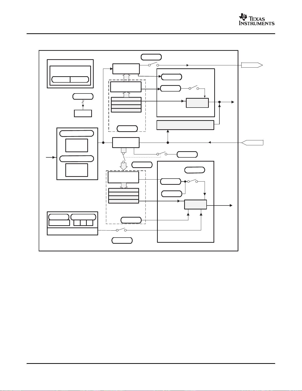
www.ti.com
ADVANCE INFORMATION
TXFIFO_0
LSPCLK
WUT
FrameFormatandMode
Even/Odd Enable
Parity
SCIRXInterruptselectlogic
BRKDT
RXRDY
SCIRXST.6
SCICTL1.3
8
SCICTL2.1
RX/BKINTENA
SCIRXD
SCIRXST.1
TXENA
SCITXInterruptselectlogic
TXEMPTY
TXRDY
SCICTL2.0
TXINTENA
SCITXD
RXENA
SCIRXD
RXWAKE
SCICTL1.6
RXERRINTENA
TXWAKE
SCITXD
SCICCR.6SCICCR.5
SCITXBUF.7-0
SCIHBAUD.15-8
BaudRate
MSbyte
Register
SCILBAUD.7-0
Transmitter-Data
BufferRegister
8
SCICTL2.6
SCICTL2.7
BaudRate
LSbyte
Register
RXSHF
Register
TXSHF
Register
SCIRXST.5
1
TXFIFO_1
-----
TXFIFO_15
8
TXFIFOregisters
TXFIFO
TXInterrupt
Logic
TXINT
SCIFFTX.14
RXFIFO_15
SCIRXBUF.7-0
ReceiveData
Bufferregister
SCIRXBUF.7-0
-----
RXFIFO_1
RXFIFO_0
8
RXFIFOregisters
SCICTL1.0
RXInterrupt
Logic
RXINT
RXFIFO
SCIFFRX.15
RXFFOVF
RXError
SCIRXST.7
PEFE OE
RXError
SCIRXST.4-2
ToCPU
ToCPU
AutoBaudDetectlogic
SCICTL1.1
SCIFFENA
Interrupts
Interrupts
TMS320F28335, TMS320F28334, TMS320F28332
TMS320F28235, TMS320F28234, TMS320F28232
Digital Signal Controllers (DSCs)
SPRS439C – JUNE 2007 – REVISED FEBRUARY 2008
Figure 4-15 shows the SCI module block diagram.
Peripherals 90 Submit Documentation Feedback
Figure 4-15. Serial Communications Interface (SCI) Module Block Diagram

www.ti.com
ADVANCE INFORMATION
4.11 Serial Peripheral Interface (SPI) Module (SPI-A)
Baud rate =
LSPCLK
4
LSPCLK
(SPIBRR ) 1)
when SPIBRR = 3 to 127
Baud rate = when SPIBRR = 0,1, 2
The devices include the four-pin serial peripheral interface (SPI) module. One SPI module (SPI-A) is
available. The SPI is a high-speed, synchronous serial I/O port that allows a serial bit stream of
programmed length (one to sixteen bits) to be shifted into and out of the device at a programmable
bit-transfer rate. Normally, the SPI is used for communications between the DSC controller and external
peripherals or another processor. Typical applications include external I/O or peripheral expansion through
devices such as shift registers, display drivers, and ADCs. Multidevice communications are supported by
the master/slave operation of the SPI.
The SPI module features include:
• Four external pins:
– SPISOMI: SPI slave-output/master-input pin
– SPISIMO: SPI slave-input/master-output pin
– SPISTE: SPI slave transmit-enable pin
– SPICLK: SPI serial-clock pin
NOTE: All four pins can be used as GPIO, if the SPI module is not used.
• Two operational modes: master and slave
Baud rate: 125 different programmable rates.
TMS320F28335, TMS320F28334, TMS320F28332
TMS320F28235, TMS320F28234, TMS320F28232
Digital Signal Controllers (DSCs)
SPRS439C – JUNE 2007 – REVISED FEBRUARY 2008
• Data word length: one to sixteen data bits
• Four clocking schemes (controlled by clock polarity and clock phase bits) include:
– Falling edge without phase delay: SPICLK active-high. SPI transmits data on the falling edge of the
SPICLK signal and receives data on the rising edge of the SPICLK signal.
– Falling edge with phase delay: SPICLK active-high. SPI transmits data one half-cycle ahead of the
falling edge of the SPICLK signal and receives data on the falling edge of the SPICLK signal.
– Rising edge without phase delay: SPICLK inactive-low. SPI transmits data on the rising edge of the
SPICLK signal and receives data on the falling edge of the SPICLK signal.
– Rising edge with phase delay: SPICLK inactive-low. SPI transmits data one half-cycle ahead of the
falling edge of the SPICLK signal and receives data on the rising edge of the SPICLK signal.
• Simultaneous receive and transmit operation (transmit function can be disabled in software)
• Transmitter and receiver operations are accomplished through either interrupt-driven or polled
algorithms.
• Nine SPI module control registers: Located in control register frame beginning at address 7040h.
NOTE
All registers in this module are 16-bit registers that are connected to Peripheral Frame 2.
When a register is accessed, the register data is in the lower byte (7-0), and the upper
byte (15-8) is read as zeros. Writing to the upper byte has no effect.
Enhanced feature:
• 16-level transmit/receive FIFO
• Delayed transmit control
The SPI port operation is configured and controlled by the registers listed in Table 4-12 .
Submit Documentation Feedback Peripherals 91

www.ti.com
ADVANCE INFORMATION
TMS320F28335, TMS320F28334, TMS320F28332
TMS320F28235, TMS320F28234, TMS320F28232
Digital Signal Controllers (DSCs)
SPRS439C – JUNE 2007 – REVISED FEBRUARY 2008
Table 4-12. SPI-A Registers
NAME ADDRESS SIZE (X16) DESCRIPTION
SPICCR 0x7040 1 SPI-A Configuration Control Register
SPICTL 0x7041 1 SPI-A Operation Control Register
SPISTS 0x7042 1 SPI-A Status Register
SPIBRR 0x7044 1 SPI-A Baud Rate Register
SPIRXEMU 0x7046 1 SPI-A Receive Emulation Buffer Register
SPIRXBUF 0x7047 1 SPI-A Serial Input Buffer Register
SPITXBUF 0x7048 1 SPI-A Serial Output Buffer Register
SPIDAT 0x7049 1 SPI-A Serial Data Register
SPIFFTX 0x704A 1 SPI-A FIFO Transmit Register
SPIFFRX 0x704B 1 SPI-A FIFO Receive Register
SPIFFCT 0x704C 1 SPI-A FIFO Control Register
SPIPRI 0x704F 1 SPI-A Priority Control Register
(1) Registers in this table are mapped to Peripheral Frame 2. This space only allows 16-bit accesses. 32-bit accesses produce undefined
results.
(1)
Peripherals 92 Submit Documentation Feedback

www.ti.com
ADVANCE INFORMATION
S
SPICTL.0
SPI INT FLAG
SPI INT
ENA
SPISTS.6
S
Clock
Polarity
Talk
LSPCLK
456 123 0
0123
SPI Bit Rate
State Control
SPIRXBUF
Buffer Register
Clock
Phase
Receiver
Overrun Flag
SPICTL.4
Overrun
INT ENA
SPICCR.3 − 0
SPIBRR.6 − 0
SPICCR.6 SPICTL.3
SPIDAT.15 − 0
SPICTL.1
M
S
M
Master/Slave
SPISTS.7
SPIDAT
Data Register
M
S
SPICTL.2
SPI Char
SPISIMO
SPISOMI
SPICLK
SW2
S
M
M
S
SW3
To CPU
M
SW1
SPITXBUF
Buffer Register
RX FIFO _0
RX FIFO _1
−−−−−
RX FIFO _15
TX FIFO registers
TX FIFO _0
TX FIFO _1
−−−−−
TX FIFO _15
RX FIFO registers
16
16
16
TX Interrupt
Logic
RX Interrupt
Logic
SPIINT/SPIRXINT
SPITXINT
SPIFFOVF FLAG
SPIFFRX.15
16
TX FIFO Interrupt
RX FIFO Interrupt
SPIRXBUF
SPITXBUF
SPIFFTX.14
SPIFFENA
SPISTE
(A)
Figure 4-16 is a block diagram of the SPI in slave mode.
TMS320F28335, TMS320F28334, TMS320F28332
TMS320F28235, TMS320F28234, TMS320F28232
Digital Signal Controllers (DSCs)
SPRS439C – JUNE 2007 – REVISED FEBRUARY 2008
Figure 4-16. SPI Module Block Diagram (Slave Mode)
A. SPISTE is driven low by the master for a slave device.
Submit Documentation Feedback Peripherals 93

www.ti.com
ADVANCE INFORMATION
TMS320F28335, TMS320F28334, TMS320F28332
TMS320F28235, TMS320F28234, TMS320F28232
Digital Signal Controllers (DSCs)
SPRS439C – JUNE 2007 – REVISED FEBRUARY 2008
4.12 Inter-Integrated Circuit (I2C)
The device contains one I2C Serial Port. Figure 4-15 shows how the I2C peripheral module interfaces
within the device.
The I2C module has the following features:
• Compliance with the Philips Semiconductors I2C-bus specification (version 2.1):
– Support for 1-bit to 8-bit format transfers
– 7-bit and 10-bit addressing modes
– General call
– START byte mode
– Support for multiple master-transmitters and slave-receivers
– Support for multiple slave-transmitters and master-receivers
– Combined master transmit/receive and receive/transmit mode
– Data transfer rate of from 10 kbps up to 400 kbps (Philips Fast-mode rate)
• One 16-bit receive FIFO and one 16-bit transmit FIFO
• One interrupt that can be used by the CPU. This interrupt can be generated as a result of one of the
following conditions:
– Transmit-data ready
– Receive-data ready
– Register-access ready
– No-acknowledgment received
– Arbitration lost
– Stop condition detected
– Addressed as slave
• An additional interrupt that can be used by the CPU when in FIFO mode
• Module enable/disable capability
• Free data format mode
Peripherals 94 Submit Documentation Feedback
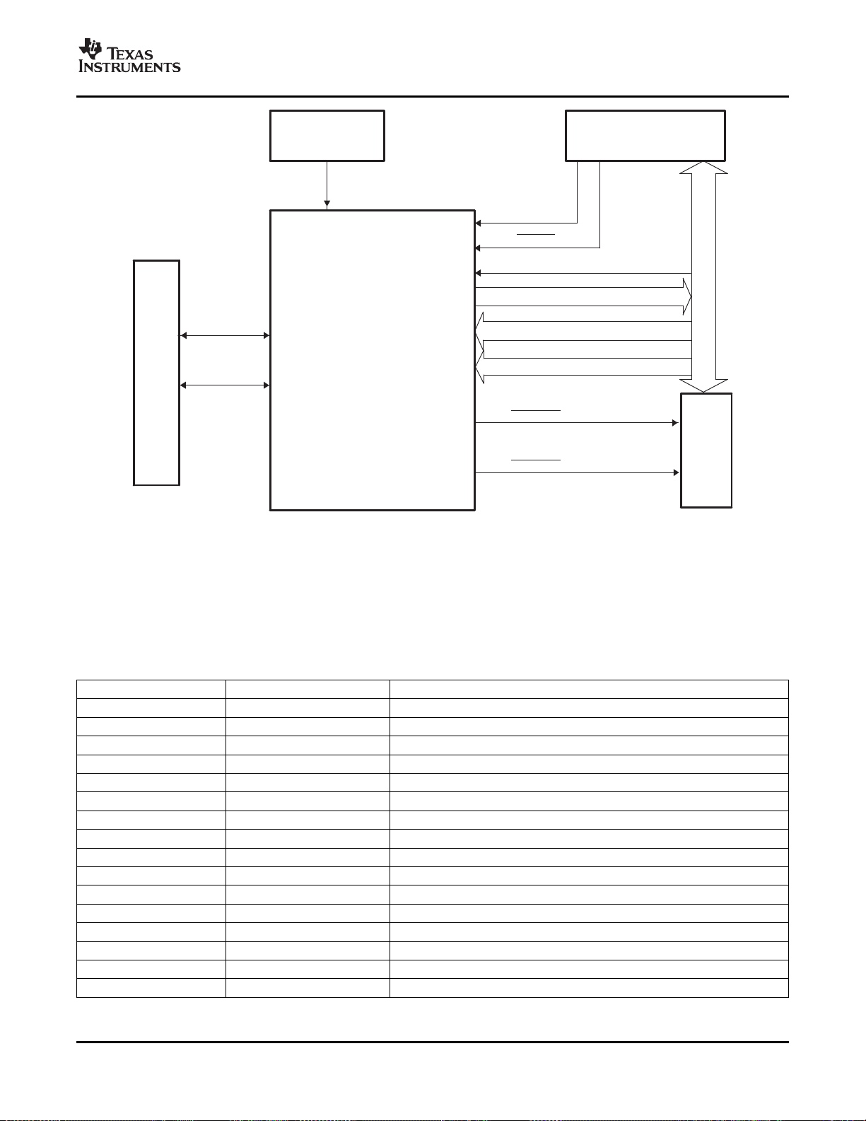
www.ti.com
ADVANCE INFORMATION
SYSRS
Data[16]
SYSCLKOUT
Data[16]
Addr[16]
Control
I2CINT1A
I2CINT2A
C28X CPU
GPIO
MUX
I2C−A
System Control
Block
I2CAENCLK
PIE
Block
SDAA
SCLA
Peripheral Bus
TMS320F28335, TMS320F28334, TMS320F28332
TMS320F28235, TMS320F28234, TMS320F28232
Digital Signal Controllers (DSCs)
SPRS439C – JUNE 2007 – REVISED FEBRUARY 2008
A. The I2C registers are accessed at the SYSCLKOUT rate. The internal timing and signal waveforms of the I2C port are
also at the SYSCLKOUT rate.
B. The clock enable bit (I2CAENCLK) in the PCLKCRO register turns off the clock to the I2C port for low power
operation. Upon reset, I2CAENCLK is clear, which indicates the peripheral internal clocks are off.
Figure 4-17. I2C Peripheral Module Interfaces
The registers in Table 4-13 configure and control the I2C port operation.
Table 4-13. I2C-A Registers
NAME ADDRESS DESCRIPTION
I2COAR 0x7900 I2C own address register
I2CIER 0x7901 I2C interrupt enable register
I2CSTR 0x7902 I2C status register
I2CCLKL 0x7903 I2C clock low-time divider register
I2CCLKH 0x7904 I2C clock high-time divider register
I2CCNT 0x7905 I2C data count register
I2CDRR 0x7906 I2C data receive register
I2CSAR 0x7907 I2C slave address register
I2CDXR 0x7908 I2C data transmit register
I2CMDR 0x7909 I2C mode register
I2CISRC 0x790A I2C interrupt source register
I2CPSC 0x790C I2C prescaler register
I2CFFTX 0x7920 I2C FIFO transmit register
I2CFFRX 0x7921 I2C FIFO receive register
I2CRSR - I2C receive shift register (not accessible to the CPU)
I2CXSR - I2C transmit shift register (not accessible to the CPU)
Submit Documentation Feedback Peripherals 95

www.ti.com
ADVANCE INFORMATION
GPxDAT(read)
Input
Qualification
GPxMUX1/2
HighImpedance
OutputControl
GPIOxpin
XRS
0=Input,1=Output
LowPower
ModesBlock
GPxDIR(latch)
Peripheral2Input
Peripheral3Input
Peripheral1Output
Peripheral2Output
Peripheral3Output
Peripheral1OutputEnable
Peripheral2OutputEnable
Peripheral3OutputEnable
00
01
10
11
00
01
10
11
00
01
10
11
GPxCTRL
Peripheral1Input
N/C
GPxPUD
LPMCR0
Internal
Pullup
GPIOLMPSEL
GPxQSEL1/2
GPxSET
GPxDAT(latch)
GPxCLEAR
GPxTOGGLE
GPIOXINT7SEL
GPIOXNMISEL
=DefaultatReset
PIE
ExternalInterrupt
MUX
Asynchronous
path
Asynchronouspath
GPIOXINT1SEL
GPIOXINT2SEL
GPIOXINT3SEL
TMS320F28335, TMS320F28334, TMS320F28332
TMS320F28235, TMS320F28234, TMS320F28232
Digital Signal Controllers (DSCs)
SPRS439C – JUNE 2007 – REVISED FEBRUARY 2008
4.13 GPIO MUX
On the F2833x/F2823x devices, the GPIO MUX can multiplex up to three independent peripheral signals
on a single GPIO pin in addition to providing individual pin bit-banging IO capability. The GPIO MUX block
diagram per pin is shown in Figure 4-18 . Because of the open drain capabilities of the I2C pins, the GPIO
MUX block diagram for these pins differ. See the TMS320F2833x Digital Signal Controller (DSC) System
Control and Interrupts Reference Guide (literature number SPRUFB0 ) for details.
A. x stands for the port, either A or B. For example, GPxDIR refers to either the GPADIR and GPBDIR register
depending on the particular GPIO pin selected.
B. GPxDAT latch/read are accessed at the same memory location.
C. This is a generic GPIO MUX block diagram. Not all options may be applicable for all GPIO pins. See the
TMS320x2833x System Control and Interrupts Reference Guide (literature number SPRUFB0 ) for pin-specific
variations.
Figure 4-18. GPIO MUX Block Diagram
Peripherals 96 Submit Documentation Feedback

www.ti.com
ADVANCE INFORMATION
TMS320F28335, TMS320F28334, TMS320F28332
TMS320F28235, TMS320F28234, TMS320F28232
Digital Signal Controllers (DSCs)
SPRS439C – JUNE 2007 – REVISED FEBRUARY 2008
The device supports 88 GPIO pins. The GPIO control and data registers are mapped to Peripheral Frame
1 to enable 32-bit operations on the registers (along with 16-bit operations). Table 4-14 shows the GPIO
register mapping.
Table 4-14. GPIO Registers
NAME ADDRESS SIZE (x16) DESCRIPTION
GPIO CONTROL REGISTERS (EALLOW PROTECTED)
GPACTRL 0x6F80 2 GPIO A Control Register (GPIO0 to 31)
GPAQSEL1 0x6F82 2 GPIO A Qualifier Select 1 Register (GPIO0 to 15)
GPAQSEL2 0x6F84 2 GPIO A Qualifier Select 2 Register (GPIO16 to 31)
GPAMUX1 0x6F86 2 GPIO A MUX 1 Register (GPIO0 to 15)
GPAMUX2 0x6F88 2 GPIO A MUX 2 Register (GPIO16 to 31)
GPADIR 0x6F8A 2 GPIO A Direction Register (GPIO0 to 31)
GPAPUD 0x6F8C 2 GPIO A Pull Up Disable Register (GPIO0 to 31)
Reserved 0x6F8E – 0x6F8F 2
GPBCTRL 0x6F90 2 GPIO B Control Register (GPIO32 to 35)
GPBQSEL1 0x6F92 2 GPIO B Qualifier Select 1 Register (GPIO32 to 35)
GPBQSEL2 0x6F94 2 Reserved
GPBMUX1 0x6F96 2 GPIO B MUX 1 Register (GPIO32 to 35)
GPBMUX2 0x6F98 2 GPIO B MUX 2 Register (GPIO48 to 63)
GPBDIR 0x6F9A 2 GPIO B Direction Register (GPIO32 to 35)
GPBPUD 0x6F9C 2 GPIO B Pull Up Disable Register (GPIO32 to 35)
Reserved 0x6F9E – 0x6FA5 8
GPCMUX1 0x6FA6 2 GPIO C MUX1 Register (GPIO64 to 79)
GPCMUX2 0x6FA8 2 GPIO C MUX2 Register (GPIO80 to 87)
GPCDIR 0x6FAA 2 GPIO C Direction Register (GPIO64 to 87)
GPCPUD 0x6FAC 2 GPIO C Pull Up Disable Register (GPIO64 to 87)
Reserved 0x6FAE – 0x6FBF 18
GPIO DATA REGISTERS (NOT EALLOW PROTECTED)
GPADAT 0x6FC0 2 GPIO A Data Register (GPIO0 to 31)
GPASET 0x6FC2 2 GPIO A Data Set Register (GPIO0 to 31)
GPACLEAR 0x6FC4 2 GPIO A Data Clear Register (GPIO0 to 31)
GPATOGGLE 0x6FC6 2 GPIO A Data Toggle Register (GPIO0 to 31)
GPBDAT 0x6FC8 2 GPIO B Data Register (GPIO32 to 35)
GPBSET 0x6FCA 2 GPIO B Data Set Register (GPIO32 to 35)
GPBCLEAR 0x6FCC 2 GPIO B Data Clear Register (GPIO32 to 35)
GPBTOGGLE 0x6FCE 2 GPIOB Data Toggle Register (GPIO32 to 35)
GPCDAT 0x6FD0 2 GPIO C Data Register (GPIO64 to 87)
GPCSET 0x6FD2 2 GPIO C Data Set Register (GPIO64 to 87)
GPCCLEAR 0x6FD4 2 GPIO C Data Clear Register (GPIO64 to 87)
GPCTOGGLE 0x6FD6 2 GPIO C Data Toggle Register (GPIO64 to 87)
Reserved 0x6FD8 0x6FDF 8
GPIO INTERRUPT AND LOW POWER MODES SELECT REGISTERS (EALLOW PROTECTED)
GPIOXINT1SEL 0x6FE0 1 XINT1 GPIO Input Select Register (GPIO0 to 31)
GPIOXINT2SEL 0x6FE1 1 XINT2 GPIO Input Select Register (GPIO0 to 31)
GPIOXNMISEL 0x6FE2 1 XNMI GPIO Input Select Register (GPIO0 to 31)
GPIOXINT3SEL 0x6FE3 1 XINT3 GPIO Input Select Register (GPIO32 to 63)
GPIOXINT4SEL 0x6FE4 1 XINT4 GPIO Input Select Register (GPIO32 to 63)
GPIOXINT5SEL 0x6FE5 1 XINT5 GPIO Input Select Register (GPIO32 to 63)
Submit Documentation Feedback Peripherals 97

www.ti.com
ADVANCE INFORMATION
TMS320F28335, TMS320F28334, TMS320F28332
TMS320F28235, TMS320F28234, TMS320F28232
Digital Signal Controllers (DSCs)
SPRS439C – JUNE 2007 – REVISED FEBRUARY 2008
Table 4-14. GPIO Registers (continued)
NAME ADDRESS SIZE (x16) DESCRIPTION
GPIOXINT6SEL 0x6FE6 1 XINT6 GPIO Input Select Register (GPIO32 to 63)
GPIOINT7SEL 0x6FE7 1 XINT7 GPIO Input Select Register (GPIO32 to 63)
GPIOLPMSEL 0x6FE8 2 LPM GPIO Select Register (GPIO0 to 31)
Reserved 0x6FEA – 0x6FFF 22
Table 4-15. GPIO-A Mux Peripheral Selection Matrix
REGISTER BITS PERIPHERAL SELECTION
GPADIR GPAMUX1 GPIOx PER1 PER2 PER3
GPADAT GPAQSEL1 GPAMUX1=0,0 GPAMUX1 = 0, 1 GPAMUX1 = 1, 0 GPAMUX1 = 1, 1
GPASET
GPACLR
GPATOGGLE
QUALPRD0 0 1, 0 GPIO0 (I/O) EPWM1A (O)
1 3, 2 GPIO1 (I/O) EPWM1B (O) ECAP6 (I/O) MFSRB (I/O)
2 5, 4 GPIO2 (I/O) EPWM2A (O)
3 7, 6 GPIO3 (I/O) EPWM2B (O) ECAP5 (I/O) MCLKRB (I/O)
4 9, 8 GPIO4 (I/O) EPWM3A (O)
5 11, 10 GPIO5 (I/O) EPWM3B (O) MFSRA (I/O) ECAP1 (I/O)
6 13, 12 GPIO6 (I/O) EPWM4A (O) EPWMSYNCI (I) EPWMSYNCO (O)
7 15, 14 GPIO7 (I/O) EPWM4B (O) MCLKRA (I/O) ECAP2 (I/O)
QUALPRD1 8 17, 16 GPIO8 (I/O) EPWM5A (O) CANTXB (O) ADCSOCAO (O)
9 19, 18 GPIO9 (I/O) EPWM5B (O) SCITXDB (O) ECAP3 (I/O)
10 21, 20 GPIO10 (I/O) EPWM6A (O) CANRXB (I) ADCSOCBO (O)
11 23, 22 GPIO11 (I/O) EPWM6B (O) SCIRXDB (I) ECAP4 (I/O)
12 25, 24 GPIO12 (I/O) TZ1 (I) CANTXB (O) MDXB (O)
13 27, 26 GPIO13 (I/O) TZ2 (I) CANRXB (I) MDRB (I)
14 29, 28 GPIO14 (I/O) TZ3 (I)/ XHOLD (I) SCITXDB (O) MCLKXB (I/O)
15 31, 30 GPIO15 (I/O) TZ4 (I)/ XHOLDA (O) SCIRXDB (I) MFSXB (I/O)
GPAMUX2 GPAMUX2 =0, 0 GPAMUX2 = 0, 1 GPAMUX2 = 1, 0 GPAMUX2 = 1, 1
GPAQSEL2
QUALPRD2 16 1, 0 GPIO16 (I/O) SPISIMOA (I/O) CANTXB (O) TZ5 (I)
17 3, 2 GPIO17 (I/O) SPISOMIA (I/O) CANRXB (I) TZ6 (I)
18 5, 4 GPIO18 (I/O) SPICLKA (I/O) SCITXDB (O) CANRXA (I)
19 7, 6 GPIO19 (I/O) SPISTEA (I/O) SCIRXDB (I) CANTXA (O)
20 9, 8 GPIO20 (I/O) EQEP1A (I) MDXA (O) CANTXB (O)
21 11, 10 GPIO21 (I/O) EQEP1B (I) MDRA (I) CANRXB (I)
22 13, 12 GPIO22 (I/O) EQEP1S (I/O) MCLKXA (I/O) SCITXDB (O)
23 15, 14 GPIO23 (I/O) EQEP1I (I/O) MFSXA (I/O) SCIRXDB (I)
QUALPRD3 24 17, 16 GPIO24 (I/O) ECAP1 (I/O) EQEP2A (I) MDXB (O)
25 19, 18 GPIO25 (I/O) ECAP2 (I/O) EQEP2B (I) MDRB (I)
26 21, 20 GPIO26 (I/O) ECAP3 (I/O) EQEP2I (I/O) MCLKXB (I/O)
27 23, 22 GPIO27 (I/O) ECAP4 (I/O) EQEP2S (I/O) MFSXB (I/O)
28 25, 24 GPIO28 (I/O) SCIRXDA (I) XZCS6 (O)
29 27, 26 GPIO29 (I/O) SCITXDA (O) XA19 (O)
30 29, 28 GPIO30 (I/O) CANRXA (I) XA18 (O)
31 31, 30 GPIO31 (I/O) CANTXA (O) XA17 (O)
Peripherals 98 Submit Documentation Feedback

www.ti.com
ADVANCE INFORMATION
TMS320F28335, TMS320F28334, TMS320F28332
TMS320F28235, TMS320F28234, TMS320F28232
Digital Signal Controllers (DSCs)
SPRS439C – JUNE 2007 – REVISED FEBRUARY 2008
Table 4-16. GPIO-B Mux Peripheral Selection Matrix
REGISTER BITS PERIPHERAL SELECTION
GPBDIR GPBMUX1 GPIOx PER1 PER2 PER3
GPBDAT GPBQSEL1 GPBMUX1=0, 0 GPBMUX1 = 0, 1 GPBMUX1 = 1, 0 GPBMUX1 = 1, 1
GPBSET
GPBCLR
GPBTOGGLE
QUALPRD0 0 1, 0 GPIO32 (I/O) SDAA (I/OC)
1 3, 2 GPIO33 (I/O) SCLA (I/OC)
2 5, 4 GPIO34 (I/O) ECAP1 (I/O) XREADY (I)
3 7, 6 GPIO35 (I/O) SCITXDA (O) XR/ W (O)
4 9, 8 GPIO36 (I/O) SCIRXDA (I) XZCS0 (O)
5 11, 10 GPIO37 (I/O) ECAP2 (I/O) XZCS7 (O)
6 13, 12 GPIO38 (I/O) XWE0 (O)
7 15, 14 GPIO39 (I/O) XA16 (O)
QUALPRD1 8 17, 16 GPIO40 (I/O) XA0/ XWE1 (O)
9 19, 18 GPIO41 (I/O) XA1 (O)
10 21, 20 GPIO42 (I/O) XA2 (O)
11 23, 22 GPIO43 (I/O) XA3 (O)
12 25, 24 GPIO44 (I/O) XA4 (O)
13 27, 26 GPIO45 (I/O) XA5 (O)
14 29, 28 GPIO46 (I/O) XA6 (O)
15 31, 30 GPIO47 (I/O) XA7 (O)
GPBMUX2 GPBMUX2 =0, 0 GPBMUX2 = 0, 1 GPBMUX2 = 1, 0 GPBMUX2 = 1, 1
GPBQSEL2
QUALPRD2 16 1, 0 GPIO48 (I/O) ECAP5 (I/O) XD31 (I/O)
17 3, 2 GPIO49 (I/O) ECAP6 (I/O) XD30 (I/O)
18 5, 4 GPIO50 (I/O) EQEP1A (I) XD29 (I/O)
19 7, 6 GPIO51 (I/O) EQEP1B (I) XD28 (I/O)
20 9, 8 GPIO52 (I/O) EQEP1S (I/O) XD27 (I/O)
21 11, 10 GPIO53 (I/O) EQEP1I (I/O) XD26 (I/O)
22 13, 12 GPIO54 (I/O) SPISIMOA (I/O) XD25 (I/O)
23 15, 14 GPIO55 (I/O) SPISOMIA (I/O) XD24 (I/O)
QUALPRD3 24 17, 16 GPIO56 (I/O) SPICLKA (I/O) XD23 (I/O)
25 19, 18 GPIO57 (I/O) SPISTEA (I/O) XD22 (I/O)
26 21, 20 GPIO58 (I/O) MCLKRA (I/O) XD21 (I/O)
27 23, 22 GPIO59 (I/O) MFSRA (I/O) XD20 (I/O)
28 25, 24 GPIO60 (I/O) MCLKRB (I/O) XD19 (I/O)
29 27, 26 GPIO61 (I/O) MFSRB (I/O) XD18 (I/O)
30 29, 28 GPIO62 (I/O) SCIRXDC (I) XD17 (I/O)
31 31, 30 GPIO63 (I/O) SCITXDC (O) XD16 (I/O)
(1) Open drain
Reserved
(1)
(1)
EPWMSYNCI (I) ADCSOCAO (O)
EPWMSYNCO (O) ADCSOCBO (O)
Submit Documentation Feedback Peripherals 99
www.ti.com
ADVANCE INFORMATION
TMS320F28335, TMS320F28334, TMS320F28332
TMS320F28235, TMS320F28234, TMS320F28232
Digital Signal Controllers (DSCs)
SPRS439C – JUNE 2007 – REVISED FEBRUARY 2008
Table 4-17. GPIO-C Mux Peripheral Selection Matrix
REGISTER BITS PERIPHERAL SELECTION
GPCDIR GPCMUX1 GPIOx or PER1 PER2 or PER3
GPCDAT GPCMUX1 = 0, 0 or 0, 1 GPCMUX1 = 1, 0 or 1, 1
GPCSET
GPCCLR
GPCTOGGLE
no qual 0 1, 0 GPIO64 (I/O) XD15 (I/O)
1 3, 2 GPIO65 (I/O) XD14 (I/O)
2 5, 4 GPIO66 (I/O) XD13 (I/O)
3 7, 6 GPIO67 (I/O) XD12 (I/O)
4 9, 8 GPIO68 (I/O) XD11 (I/O)
5 11, 10 GPIO69 (I/O) XD10 (I/O)
6 13, 12 GPIO70 (I/O) XD9 (I/O)
7 15, 14 GPIO71 (I/O) XD8 (I/O)
no qual 8 17, 16 GPIO72 (I/O) XD7 (I/O)
9 19, 18 GPIO73 (I/O) XD6 (I/O)
10 21, 20 GPIO74 (I/O) XD5 (I/O)
11 23, 22 GPIO75 (I/O) XD4 (I/O)
12 25, 24 GPIO76 (I/O) XD3 (I/O)
13 27, 26 GPIO77 (I/O) XD2 (I/O)
14 29, 28 GPIO78 (I/O) XD1 (I/O)
15 31, 30 GPIO79 (I/O) XD0 (I/O)
GPCMUX2 GPCMUX2 = 0, 0 or 0, 1 GPCMUX2 = 1, 0 or 1, 1
no qual 16 1, 0 GPIO80 (I/O) XA8 (O)
17 3, 2 GPIO81 (I/O) XA9 (O)
18 5, 4 GPIO82 (I/O) XA10 (O)
19 7, 6 GPIO83 (I/O) XA11 (O)
20 9, 8 GPIO84 (I/O) XA12 (O)
21 11, 10 GPIO85 (I/O) XA13 (O)
22 13, 12 GPIO86 (I/O) XA14 (O)
23 15, 14 GPIO87 (I/O) XA15 (O)
The user can select the type of input qualification for each GPIO pin via the GPxQSEL1/2 registers from
four choices:
• Synchronization To SYSCLKOUT Only (GPxQSEL1/2=0, 0): This is the default mode of all GPIO pins
at reset and it simply synchronizes the input signal to the system clock (SYSCLKOUT).
• Qualification Using Sampling Window (GPxQSEL1/2=0, 1 and 1, 0): In this mode the input signal, after
synchronization to the system clock (SYSCLKOUT), is qualified by a specified number of cycles before
the input is allowed to change.
Peripherals 100 Submit Documentation Feedback
 Loading...